WO2023053836A1 - 圧電振動デバイス - Google Patents
圧電振動デバイス Download PDFInfo
- Publication number
- WO2023053836A1 WO2023053836A1 PCT/JP2022/032821 JP2022032821W WO2023053836A1 WO 2023053836 A1 WO2023053836 A1 WO 2023053836A1 JP 2022032821 W JP2022032821 W JP 2022032821W WO 2023053836 A1 WO2023053836 A1 WO 2023053836A1
- Authority
- WO
- WIPO (PCT)
- Prior art keywords
- substrate
- vibration device
- vibrator
- piezoelectric vibration
- external connection
- Prior art date
- Legal status (The legal status is an assumption and is not a legal conclusion. Google has not performed a legal analysis and makes no representation as to the accuracy of the status listed.)
- Ceased
Links
Images




Classifications
-
- H—ELECTRICITY
- H03—ELECTRONIC CIRCUITRY
- H03H—IMPEDANCE NETWORKS, e.g. RESONANT CIRCUITS; RESONATORS
- H03H9/00—Networks comprising electromechanical or electro-acoustic elements; Electromechanical resonators
- H03H9/02—Details
- H03H9/05—Holders or supports
- H03H9/0538—Constructional combinations of supports or holders with electromechanical or other electronic elements
- H03H9/0542—Constructional combinations of supports or holders with electromechanical or other electronic elements consisting of a lateral arrangement
-
- H—ELECTRICITY
- H03—ELECTRONIC CIRCUITRY
- H03B—GENERATION OF OSCILLATIONS, DIRECTLY OR BY FREQUENCY-CHANGING, BY CIRCUITS EMPLOYING ACTIVE ELEMENTS WHICH OPERATE IN A NON-SWITCHING MANNER; GENERATION OF NOISE BY SUCH CIRCUITS
- H03B5/00—Generation of oscillations using amplifier with regenerative feedback from output to input
- H03B5/30—Generation of oscillations using amplifier with regenerative feedback from output to input with frequency-determining element being electromechanical resonator
- H03B5/32—Generation of oscillations using amplifier with regenerative feedback from output to input with frequency-determining element being electromechanical resonator being a piezoelectric resonator
-
- H—ELECTRICITY
- H03—ELECTRONIC CIRCUITRY
- H03H—IMPEDANCE NETWORKS, e.g. RESONANT CIRCUITS; RESONATORS
- H03H9/00—Networks comprising electromechanical or electro-acoustic elements; Electromechanical resonators
- H03H9/02—Details
- H03H9/05—Holders or supports
- H03H9/0538—Constructional combinations of supports or holders with electromechanical or other electronic elements
- H03H9/0547—Constructional combinations of supports or holders with electromechanical or other electronic elements consisting of a vertical arrangement
-
- H—ELECTRICITY
- H03—ELECTRONIC CIRCUITRY
- H03H—IMPEDANCE NETWORKS, e.g. RESONANT CIRCUITS; RESONATORS
- H03H9/00—Networks comprising electromechanical or electro-acoustic elements; Electromechanical resonators
- H03H9/02—Details
- H03H9/05—Holders or supports
- H03H9/0538—Constructional combinations of supports or holders with electromechanical or other electronic elements
- H03H9/0547—Constructional combinations of supports or holders with electromechanical or other electronic elements consisting of a vertical arrangement
- H03H9/0552—Constructional combinations of supports or holders with electromechanical or other electronic elements consisting of a vertical arrangement the device and the other elements being mounted on opposite sides of a common substrate
-
- H—ELECTRICITY
- H03—ELECTRONIC CIRCUITRY
- H03H—IMPEDANCE NETWORKS, e.g. RESONANT CIRCUITS; RESONATORS
- H03H9/00—Networks comprising electromechanical or electro-acoustic elements; Electromechanical resonators
- H03H9/02—Details
- H03H9/05—Holders or supports
- H03H9/10—Mounting in enclosures
- H03H9/1007—Mounting in enclosures for bulk acoustic wave [BAW] devices
- H03H9/1014—Mounting in enclosures for bulk acoustic wave [BAW] devices the enclosure being defined by a frame built on a substrate and a cap, the frame having no mechanical contact with the BAW device
- H03H9/1021—Mounting in enclosures for bulk acoustic wave [BAW] devices the enclosure being defined by a frame built on a substrate and a cap, the frame having no mechanical contact with the BAW device the BAW device being of the cantilever type
-
- H—ELECTRICITY
- H03—ELECTRONIC CIRCUITRY
- H03H—IMPEDANCE NETWORKS, e.g. RESONANT CIRCUITS; RESONATORS
- H03H9/00—Networks comprising electromechanical or electro-acoustic elements; Electromechanical resonators
- H03H9/15—Constructional features of resonators consisting of piezoelectric or electrostrictive material
- H03H9/17—Constructional features of resonators consisting of piezoelectric or electrostrictive material having a single resonator
- H03H9/19—Constructional features of resonators consisting of piezoelectric or electrostrictive material having a single resonator consisting of quartz
-
- H—ELECTRICITY
- H10—SEMICONDUCTOR DEVICES; ELECTRIC SOLID-STATE DEVICES NOT OTHERWISE PROVIDED FOR
- H10W—GENERIC PACKAGES, INTERCONNECTIONS, CONNECTORS OR OTHER CONSTRUCTIONAL DETAILS OF DEVICES COVERED BY CLASS H10
- H10W90/00—Package configurations
Definitions
- the present invention relates to piezoelectric vibration devices.
- a piezoelectric vibration device includes, for example, a crystal oscillator using a crystal vibrating piece.
- the crystal oscillator includes a crystal vibrating piece that is a piezoelectric element, a holding member that holds the crystal vibrating piece, and a lid member that seals the holding member.
- the crystal vibrating piece is held in the box-shaped holding member made of an insulating material such as ceramic.
- the crystal vibrating piece in the holding member is hermetically sealed by a lid member in a state in which the electrodes of the crystal vibrating piece and the electrodes of the holding member are joined.
- a piezoelectric diaphragm having a vibrating portion having a first excitation electrode and a second excitation electrode and an outer frame portion connected to the vibrating portion via a connecting portion and surrounding the vibrating portion is a sealing member.
- Encapsulated piezoelectric vibrators are known.
- the piezoelectric vibrator having a laminated structure in which the piezoelectric diaphragm having the vibrating portion is sealed with a sealing member can reduce the thickness of the piezoelectric vibrator itself.
- the piezoelectric vibration device described in Patent Document 1 includes a crystal oscillator and an electronic component in which a first sealing member, a second sealing member, and a crystal diaphragm having excitation electrodes formed on both main surfaces are laminated.
- the element is mounted on a function section, which is a board connected to an external board.
- a crystal oscillator and an electronic component element mounted on one main surface of the function section are electrically connected to a mounting surface of an external substrate via the function section.
- One main surface of the function section has a circuit pattern for electrically connecting the crystal resonator and the electronic component element.
- the other main surface of the function section has external connection terminals electrically connected to the external substrate.
- the external connection terminals of the function section are joined to the connection terminals of the external substrate via solder or the like. That is, the function section is joined to the external substrate in a state in which the external connection terminals, the solder, and the connection terminals of the external substrate are laminated on the mounting surface of the external substrate. Furthermore, the crystal oscillator having a laminated structure is mounted on the function section.
- a piezoelectric vibration device such as the function part, in which external connection terminals are formed on the outer bottom surface of a substrate that is connected to an external substrate, has an increased total height, which increases the moment generated by external shocks, vibrations, and the like. . That is, in the piezoelectric vibration device, as the overall height increases, the force generated by the moment, which separates the external connection terminal from the connection terminal of the external substrate, increases.
- An object of the present invention is to provide a piezoelectric vibration device that can be firmly bonded to the external substrate at a position as close to the external substrate as possible.
- the piezoelectric vibration device comprises an insulating substrate having external connection terminals that are electrically connected, and at least a piezoelectric vibrator and an integrated circuit element having an oscillation circuit mounted thereon.
- the insulating substrate has a recess on the other main surface.
- the external connection terminal is positioned within the recess, and a gap is provided between the outer edge of the external connection terminal and the side surface of the recess.
- the piezoelectric vibration device is coupled at a position closer to the external substrate than when the external connection terminal is not positioned within the recess. That is, the piezoelectric vibration device can have a lower overall height than when the external connection terminal is not positioned within the recess.
- the external connection terminal is bonded to the external substrate in a gap between the side surface of the recess in the insulating substrate and the end surface including the outer edge of the external connection terminal. Joining material such as solder enters.
- the external connection terminal is bonded to the external connection terminal by the bonding material not only at the bonding surface to be connected to the external connection terminal but also at the end surface of the external connection terminal.
- the piezoelectric vibration device can be firmly bonded to the external substrate at a position as close to the external substrate as possible.
- the piezoelectric vibration device of the present invention preferably includes the following configuration.
- the external connection terminal is positioned within the recess at a predetermined distance from the outer edge of the recess when viewed in a direction perpendicular to the other main surface.
- the bottom surface of the recess is exposed over a predetermined width from the outer edge of the recess so that the external connection terminal surrounds the external connection terminal when viewed in the direction perpendicular to the other main surface. Therefore, not only the joint surface of the external connection terminal connected to the external substrate by the joint material, but also the end surface of the external connection terminal and the bottom surface of the recess are connected to the external substrate. As a result, the piezoelectric vibration device can be firmly bonded to the external substrate at a position as close to the external substrate as possible.
- the piezoelectric vibration device of the present invention preferably includes the following configuration.
- the thickness from the one main surface to the joint surface electrically connected to the external substrate at the external connection terminal is less than the thickness from the one main surface to the other main surface.
- the joint surface of the external connection terminal connected to the external substrate does not protrude from the other main surface of the insulating substrate. Therefore, the piezoelectric vibration device is coupled at a position closer to the external substrate than when the external connection terminals are located on the other main surface. As a result, the piezoelectric vibration device can be firmly bonded to the external substrate at a position as close to the external substrate as possible.
- the piezoelectric vibration device of the present invention preferably includes the following configuration. At least one of the piezoelectric vibrator and the integrated circuit element on one main surface of the insulating substrate is partially or wholly covered with resin.
- the piezoelectric vibration device in the piezoelectric vibration device, at least one of the piezoelectric vibrator and the integrated circuit element is partly or entirely formed of resin together with the insulating substrate. At least one of the vibrator and the integrated circuit element can be protected. Moreover, since the rigidity of the insulating substrate is improved by resin molding, the external connection terminals are less likely to bend due to impact and vibration. Thereby, the piezoelectric vibration device can be firmly bonded to the external substrate.
- the piezoelectric vibration device of the present invention preferably includes the following configuration.
- the insulating substrate of the internal wiring electrically connecting the wiring pattern and the external connection terminal, a part located on the other main surface side is not covered with the base material of the insulating substrate. Exposed.
- part of the internal wiring that connects the wiring pattern on the one main surface and the external connection terminal on the other main surface is not covered with an insulating member.
- the bonding member is bonded to the internal wiring exposed in the recess in a raised state. Thereby, the piezoelectric vibration device is firmly bonded to the external substrate.
- the piezoelectric vibration device of the present invention preferably includes the following configuration.
- the vibrator and the integrated circuit element are located on the same mounting surface of the insulating substrate.
- the piezoelectric vibrator and the integrated circuit element are positioned on the same mounting surface of the insulating substrate, the piezoelectric vibrator is positioned on one main surface of the insulating substrate.
- the overall height can be reduced compared to the configuration in which the integrated circuit elements are respectively located on the other main surface. Therefore, the piezoelectric vibration device can be bonded to the external substrate at a position as close as possible to the external substrate.
- the external connection terminals are less likely to peel off from the external substrate even when external shocks and vibrations are applied.
- FIG. 1 is a plan view of a piezoelectric vibration device according to Embodiment 1 of the present invention.
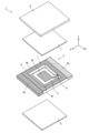
- FIG. 2 is an exploded perspective view of a vibrator in the piezoelectric vibration device according to Embodiment 1 of the present invention.
- 3 is a plan view of a vibrator in the piezoelectric vibration device according to Embodiment 1 of the present invention.
- FIG. 4 is a cross-sectional view taken along the arrow A in FIG. 3.
- FIG. 5 is a cross-sectional view of the piezoelectric vibration device according to Embodiment 1 of the present invention, taken along arrow A in FIG. 3, in a state in which resin is molded in a mold.
- FIG. 1 is a plan view of a piezoelectric vibration device according to Embodiment 1 of the present invention.
- FIG. 2 is an exploded perspective view of a vibrator in the piezoelectric vibration device according to Embodiment 1 of the present invention.
- 3 is a plan view of
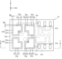
- FIG. 6 is a bottom view of the piezoelectric vibration device according to Embodiment 1 of the present invention.
- 7 is a cross-sectional view taken along arrow B in FIG. 6.
- FIG. 8 is a side view showing a state in which the external connection terminals of the piezoelectric vibration device according to Embodiment 1 of the present invention are in contact with solder on the connection terminals of the external substrate.
- FIG. 9 is a side view showing a state in which the external connection terminals of the piezoelectric vibration device according to Embodiment 1 of the present invention are joined to the external substrate by solder on the connection terminals of the external substrate.
- 10 is a cross-sectional view taken along line C in FIG. 9. FIG. FIG. FIG.
- FIG. 11 is a side view of a vibrator in a piezoelectric vibration device according to Embodiment 2 of the present invention.
- 12 is a cross-sectional view taken along line D in FIG. 11.
- FIG. 13 is a bottom view of a vibrator in a piezoelectric vibration device according to Embodiment 2 of the present invention.
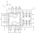
- FIG. 14 is a plan view of a piezoelectric vibration device according to Embodiment 2 of the present invention.
- 15 is a plan view of a substrate in a piezoelectric vibration device according to Embodiment 2 of the present invention.
- FIG. 16 is a cross-sectional view taken along line E in FIG. 15.
- FIG. 15 is a plan view of a substrate in a piezoelectric vibration device according to Embodiment 2 of the present invention.
- the term "principal surface” refers to the surface of the target member having the largest area, or the surface of the plate-shaped member having the largest area visible when viewed in the thickness direction.
- the longitudinal direction of the vibrator 2 and the substrate 11 is the “X direction”
- the lateral direction is the “Y direction”
- the frame portion of the vibrator 2 4 the direction perpendicular to the X direction and the Y direction and the direction perpendicular to the main surface of the substrate 11 are defined as "Z direction”.
- the X direction and the Y direction are directions on the horizontal plane.
- the Z direction is the vertical direction.
- this definition of direction is not intended to limit the orientation of the piezoelectric vibration device 1 during use.
- fixed are not limited to cases where members are directly fixed to each other, but also other It also includes the case where it is fixed via a member. That is, in the following description, expressions such as fixing include meanings such as direct and indirect fixing between members.
- FIG. 1 is a plan view showing an outline of the overall configuration of the piezoelectric vibration device 1.
- FIG. 2 is an exploded perspective view showing an outline of the overall configuration of the vibrator 2 in the piezoelectric vibrating device 1.
- FIG. 3 is a plan view of the vibrator 2.
- FIG. 4 is a cross-sectional view taken along the arrow A in FIG. 3.
- FIG. 5 is a cross-sectional view taken along the arrow A in FIG. 3 in a state where the piezoelectric vibration device 1 is resin-molded in the mold W.
- FIG. FIG. 6 is a bottom view showing an outline of the overall configuration of the piezoelectric vibration device 1.
- the piezoelectric vibration device 1 has a vibrator 2, an integrated circuit element 10, a substrate 11, and a mold portion 12 (see FIG. 5).
- the vibrator 2 is a piezoelectric element having a piezoelectric body that converts applied force into voltage or converts applied voltage into force.
- the vibrator 2 has a piezoelectric diaphragm 3 , a first sealing member 7 , a second sealing member 8 and a protective member 9 .
- the piezoelectric diaphragm 3 is a rectangular crystal vibrating piece cut out of crystal in a specific direction.
- the piezoelectric diaphragm 3 has a frame portion 4 , a vibrating portion 5 and a connecting portion 6 .
- the piezoelectric diaphragm 3 has a frame portion 4, a vibrating portion 5, and a connecting portion 6 integrally formed. That is, the frame portion 4, the vibrating portion 5, and the connecting portion 6 are configured as a single member.
- the frame part 4 is a member that surrounds the vibrating part 5.
- the frame portion 4 is made of a rectangular plate material in plan view in a direction perpendicular to the pair of main surfaces having the largest area.
- the frame portion 4 is a frame-shaped member having a rectangular opening on each of the pair of main surfaces when viewed in the Z direction, which is a plan view. That is, the frame portion 4 has a rectangular through hole 4c penetrating from one main surface toward the other main surface.
- the distance between the pair of main surfaces of the frame portion 4, which is the thickness of the frame portion 4, is the thickness t1.
- One main surface of the frame portion 4 has a first joint surface 4 a that is joined to the first sealing member 7 .
- the other main surface of the frame portion 4 has a second joint surface 4 b that joins with the second sealing member 8 .
- Both ends of the frame portion 4 in the longitudinal direction each have a vibrator mounting terminal 4d.
- the vibration part 5 is a piezoelectric body.
- the vibrating portion 5 is a substantially rectangular plate member in plan view in a direction perpendicular to the pair of principal surfaces having the largest area.
- the vibrating portion 5 is positioned within the frame of the frame portion 4 .
- the vibrating section 5 is positioned so that the pair of main surfaces face the opening of the frame section 4 when viewed in the Z direction, which is a plan view.
- the main surface of the vibrating portion 5 is positioned substantially parallel to the main surface of the frame portion 4 .
- the distance between the pair of main surfaces of the vibrating portion 5, which is the thickness of the vibrating portion 5, is a thickness t2 that is thinner than the thickness t1 of the frame portion 4. As shown in FIG.
- the vibrating portion 5 is positioned between the pair of main surfaces of the frame portion 4 within the frame of the frame portion 4 .
- a part of the vibrating section 5 is connected to the frame section 4 via a plate-like connecting section 6 .
- the vibrating portion 5 is held in a cantilevered state on the frame portion 4 via the connecting portion 6 . That is, the vibrating portion 5 is surrounded by the frame portion 4 with the through hole 4c interposed therebetween.
- One main surface of the vibrating portion 5 has a first excitation electrode 5a.
- the other main surface of the vibrating portion 5 has a second excitation electrode 5b.
- the first excitation electrode 5a is connected to one vibrator mounting terminal 4d.
- the second excitation electrode 5b is connected to the other vibrator mounting terminal 4d.
- the first sealing member 7 and the second sealing member 8 that are sealing members are members that seal the inside of the frame portion 4 .
- the first sealing member 7 and the second sealing member 8 are resin films having a rectangular shape in plan view in a direction perpendicular to the pair of main surfaces having the largest area.
- the first sealing member 7 and the second sealing member 8 are, for example, polyimide resin films having heat resistance of about 300.degree.
- the first sealing member 7 and the second sealing member 8 have a thickness t3 of about 20 ⁇ m to 50 ⁇ m.
- the width X3 in the X direction, which is the longitudinal direction, of the first sealing member 7 and the second sealing member 8 is smaller than the width X1 in the X direction at the outer edge of the frame portion 4 when viewed in the Z direction, which is a plan view, It is larger than the width X2 in the X direction at the opening portion which is the inner edge of the frame portion 4 .
- the Y-direction width Y3 of the first sealing member 7 and the second sealing member 8, which is the lateral direction perpendicular to the X-direction is equal to the Y-direction width Y1 at the outer edge of the frame portion 4 when viewed in the Z direction. and larger than the width Y2 in the Y direction at the opening portion which is the inner edge of the frame portion 4 . That is, the first sealing member 7 and the second sealing member 8 are smaller than the frame portion 4 and larger than the opening of the frame portion 4 .
- the first sealing member 7 is joined to the first joining surface 4a provided on one main surface of the frame portion 4 with a joining material 13 that is a thermoplastic adhesive.
- the peripheral edge of the first sealing member 7 is located inside the outer edge of the frame portion 4 and outside the inner edge of the frame portion 4 .
- An end portion of the first sealing member 7 in the X direction is joined to a first joint surface 4 a located in the X direction on one main surface of the frame portion 4 .
- a Y-direction end portion of the first sealing member 7 is joined to a first joint surface 4 a located in the Y-direction on one main surface of the frame portion 4 .
- the portion of the first sealing member 7 that overlaps the first bonding surface 4 a when viewed in the Z direction is bonded to the frame portion 4 with the bonding material 13 .
- the first sealing member 7 covers the opening on one main surface of the frame 4 . Thereby, the first sealing member 7 closes the opening on one main surface of the frame portion 4 .
- the second sealing member 8 is joined by a joining material 13 to the second joining surface 4b of the other main surface of the frame portion 4. As shown in FIG. The peripheral edge of the second sealing member 8 is located inside the outer edge of the frame portion 4 and outside the inner edge of the frame portion 4 .
- the X-direction end portion of the second sealing member 8 is joined to a second joint surface 4 b located in the X-direction on the other main surface of the frame portion 4 .
- a Y-direction end of the second sealing member 8 is joined to a second joint surface 4 b located in the Y-direction on the other main surface of the frame portion 4 .
- the portion of the second sealing member 8 that overlaps the second bonding surface 4 b when viewed in the Z direction is bonded to the frame portion 4 with the bonding material 13 .
- the second sealing member 8 covers the opening on one main surface of the frame portion 4 . Thereby, the second sealing member 8 closes the opening portion of the other main surface of the frame portion 4 .
- the protective member 9 is a member that suppresses bending of at least the first sealing member 7 out of the first sealing member 7 or the second sealing member 8 due to the molding pressure of the resin forming the mold portion 12 .
- the protective member 9 is a plate-like member that is rectangular in plan view in a direction perpendicular to the pair of main surfaces having the largest area.
- the protective member 9 is made of silicon, which is a brittle material. It is desirable that the protective member 9 have such a rigidity that the maximum deflection is 20 ⁇ m or less in the case of being supported on both sides in the longitudinal direction when pressure generated during molding of the resin is applied.
- the protective member 9 is made of silicon. Moreover, in the present embodiment, the protective member 9 preferably has a thickness t4 of about 30 ⁇ m to 100 ⁇ m. A thickness t4 of the protection member 9 is thicker than a thickness t3 of the first sealing member 7 and the second sealing member 8 .
- the width X4 in the X direction which is the longitudinal direction of the protective member 9, is smaller than the width X1 in the X direction at the outer edge of the frame portion 4 of the piezoelectric diaphragm 3. is greater than the width X3 of Further, when viewed in the Z direction, the Y-direction width Y4 of the protective member 9 perpendicular to the X-direction is smaller than the Y-direction width Y1 of the outer edge of the frame portion 4, and the Y width of the first sealing member 7 greater than the direction width Y3. That is, the protective member 9 is smaller than the frame portion 4 and larger than the first sealing member 7 .
- the protective member 9 is bonded to the surface of the first sealing member 7 perpendicular to the Z direction with a thermoplastic adhesive or die attach agent as a bonding material 13 .
- the peripheral edge of the protective member 9 is positioned between the peripheral edge of the first sealing member 7 and the outer edge of the frame portion 4 . That is, the peripheral portion of the protective member 9 overlaps the first joint surface 4a of the frame portion 4 when viewed in the Z direction.
- the protective member 9 is supported by the frame portion 4 at its peripheral portion.
- the protective member 9 covers the opening portion of one main surface of the frame portion 4 with the first sealing member 7 interposed therebetween. In other words, the protective member 9 covers the entire first sealing member 7 including the portion overlapping the opening when viewed in the Z direction.
- the vibrator 2 configured as described above includes a piezoelectric diaphragm 3 , a first sealing member 7 that closes an opening of one principal surface of the piezoelectric diaphragm 3 , and the other principal surface of the piezoelectric diaphragm 3 . , and a second sealing member 8 that closes the opening of the .
- the vibrator 2 has an internal space S defined by the frame portion 4 of the piezoelectric diaphragm 3 , the first sealing member 7 and the second sealing member 8 .
- the vibrator 2 has a vibrating portion 5 located within an internal space S. As shown in FIG. In addition, the internal space S is filled with an inert gas such as nitrogen gas.
- the vibrator 2 oscillates at a predetermined frequency by voltage applied from each vibrator mounting terminal 4d.
- the integrated circuit element 10 is an IC that controls the vibrator 2 .
- the integrated circuit element 10 has an electronic circuit such as an oscillation circuit that is connected to a temperature sensing element (thermistor) that detects the ambient temperature state and generates a predetermined oscillation output.
- the integrated circuit element 10 outputs the oscillation output generated by the oscillation circuit to the outside through the integrated circuit element mounting terminal 10a as a reference signal such as a clock signal.
- the integrated circuit element 10 is covered with resin except for the integrated circuit element mounting terminals 10a.
- the substrate 11 is an insulating substrate that electrically connects the vibrator 2 and the integrated circuit element 10 with a wiring pattern (not shown) and integrates them.
- the substrate 11 is made of a resin material.
- the substrate 11 is based on, for example, glass epoxy resin, which is an insulator and can be easily processed such as cutting.
- the substrate 11 can easily constitute the piezoelectric vibration device 1 having any shape.
- the substrate 11 is a rectangular plate material. In this embodiment, the thickness of the substrate 11 is, for example, 0.17 mm.
- One of the pair of main surfaces of the substrate 11 is configured as a first mounting surface 11a having the wiring pattern including pads, lands, etc. formed of a conductor such as copper.
- the vibrator 2 and the integrated circuit element 10 are mounted on the first mounting surface 11a of the substrate 11, respectively. Both vibrator mounting terminals 4d of the vibrator 2 are electrically connected to wiring patterns on the first mounting surface 11a by conductive bonding materials 13, respectively.
- the vibrator 2 is arranged with the main surface covered with the first sealing member 7 and the second sealing member 8 directed in the Z direction.
- the vibrator 2 is positioned so that the second sealing member 8 faces the first mounting surface 11a.
- the second sealing member 8 is in contact with the first mounting surface 11a.
- the integrated circuit element mounting terminals 10a of the integrated circuit element 10 are electrically connected to wiring patterns on the first mounting surface 11a of the substrate 11 by conductive bonding materials 13, respectively.
- the vibrator 2 and the integrated circuit element 10 are positioned side by side on the first mounting surface 11 a of the substrate 11 .
- the other main surface of the substrate 11 parallel to the other main surface is configured as a second mounting surface 11b having external connection terminals 11d for mounting on the external substrate P.
- the external connection terminal 11d is a plate-like terminal made of a conductive metal.
- the wiring pattern on the first mounting surface 11a is electrically connected to the external connection terminal 11d through the internal wiring 11c.
- the vibrator 2 mounted on the substrate 11 is connected to the external substrate P from the vibrator mounting terminal 4d via the wiring pattern (not shown) on the first mounting surface 11a, the internal wiring 11c, and the external connection terminal 11d on the second mounting surface 11b. (see FIG. 9). Further, the vibrating portion 5 of the vibrator 2 is held in a cantilevered state on the frame portion 4 of the piezoelectric diaphragm 3 by the connecting portion 6 . Thereby, the vibration part 5 oscillates at a predetermined frequency by the voltage applied from the external substrate P. As shown in FIG.
- the mold section 12 protects at least the oscillator 2 among the substrate 11 and the oscillator 2 and the integrated circuit element 10 mounted on the substrate 11 (see FIG. 6).
- the mold part 12 is a thermosetting resin such as an epoxy resin 12a.
- the molded portion 12 covers the substrate 11 and at least a portion of the oscillator 2 among the oscillator 2 and the integrated circuit element 10 mounted on the substrate 11 with a thermoset epoxy resin 12a.
- the mold part 12 covers the substrate 11 and the vibrator 2 and the integrated circuit element 10 mounted on the substrate 11 .
- the piezoelectric vibrating plate 3 supporting the vibrating portion 5 thinner than the frame portion 4 within the frame of the frame portion 4 is a first sealing made of a resin film. It has a three-layer structure vibrator 2 covered with a member 7 and a second sealing member 8 . Therefore, the piezoelectric vibration device 1 can be made lower in overall height than a piezoelectric vibration device having a vibrator in which a vibrating portion held by a box-shaped holding member is sealed with a lid member.
- the protective member 9 covers the first sealing member 7 with its peripheral edge supported by the frame portion 4 . Since the vibrator 2 covers the first sealing member 7 with the protective member 9, the resistance of the first sealing member 7 to the molding pressure from the mold resin is improved.
- FIG. 7 is a cross-sectional view taken along arrow B in FIG. 6.
- FIG. 7 it is assumed that the second mounting surface 11b has four external connection terminals 11d.
- the second mounting surface 11b of the substrate 11 is the other main surface electrically connected to the external substrate P.
- the second mounting surface 11b has four recesses 11g corresponding to the four external connection terminals 11d.
- the four recesses 11g are stepped portions whose arbitrarily determined range is recessed in a direction perpendicular to the second mounting surface 11b.
- the four recesses 11g have a bottom surface 11h parallel to the second mounting surface 11b and side surfaces 11i perpendicular to the second mounting surface 11b.
- the four recesses 11g are positioned at four corners including vertexes that are intersections of the long sides and the short sides of the substrate 11 when viewed in the Z direction.
- the four recesses 11g are recessed in ranges including part of the long side and part of the short side, which are the outer edge of the substrate 11 extending from the apex.
- three recesses 11g out of the four recesses 11g are rectangular when viewed in the Z direction.
- Another recess 11g of the four recesses 11g is pentagonal.
- the external connection terminal 11d is configured as a terminal that connects to the connection terminal P1 of the external substrate P on one main surface.
- the four external connection terminals 11d are positioned in the four recesses 11g, respectively.
- the external connection terminal 11d has, as viewed in the Z direction, a joint surface 11e that is joined to the connection terminal P1 on its main surface.
- the joint surface 11 e is exposed without being covered with the insulating base material of the substrate 11 .
- the joint surface 11e is parallel to the second mounting surface 11b.
- the external connection terminal 11d has a shape smaller than the bottom surface 11h when viewed in the Z direction. Therefore, the external connection terminals 11d are included in the bottom surface 11h when viewed in the Z direction. Furthermore, the external connection terminal 11d is positioned within the recess 11g with a predetermined distance from the outer edge of the bottom surface 11h. That is, the end faces 11f including the four end faces 11fa, 11fb, 11fc, and 11fd including the outer edges of the external connection terminals 11d are arranged so that a predetermined gap G is formed inside the recess 11g from the outer edge of the bottom face 11h when viewed in the Z direction. Located away from.
- An end surface 11fa adjacent to one side surface 11i and an end surface 11fb adjacent to the other side surface 11i of the concave portion 11g are positioned with a gap G1 from the side surface 11i when viewed in the Z direction.
- An end surface 11fc adjacent to the short side of the substrate 11 and an end surface 11fd adjacent to the long side of the substrate 11 included in the concave portion 11g have a predetermined gap G2 between the long side or the short side of the substrate 11 when viewed in the Z direction. It is located vacant.
- the external connection terminal 11d has four exposed end faces 11fa, 11fb, 11fc, and 11fd forming the outer edge.
- a bottom surface 11h of the recess 11g is exposed around the external connection terminal 11d.
- a groove is formed around the external connection terminal 11d by the side surface 11i of the recess 11g, the bottom surface 11h of the recess 11g, and the end surface 11f of the external connection terminal 11d.
- An internal wiring 11c is connected to the external connection terminal 11d.
- the internal wiring 11c is made of a conductive metal.
- the internal wiring 11c electrically connects the wiring pattern of the first mounting surface 11a and the external connection terminal 11d.
- the internal wiring 11c passes through the inside of the substrate 11 and is positioned within the recess 11g.
- the internal wiring 11c is connected to at least one of the four end surfaces 11fa, 11fb, 11fc, and 11fd of the external connection terminal 11d inside the recess 11g.
- the internal wiring 11c protrudes from the connected end face 11f toward the side face 11i of the recess 11g when viewed in the Z direction. Further, the internal wiring 11c does not protrude beyond the joint surface 11e of the external connection terminal 11d. Further, the internal wiring 11c is not covered with the base material of the substrate 11 inside the recess 11g. That is, the internal wiring 11c is exposed without being covered with the insulating base material of the substrate 11, like the external connection
- the thickness t1 from the first mounting surface 11a of the substrate 11 to the joint surface 11e of the external connection terminal 11d is less than the thickness t0 of the substrate 11, which is the thickness from the first mounting surface 11a to the second mounting surface 11b. That is, the joint surface 11 e of the external connection terminal 11 d does not protrude beyond the second mounting surface 11 b of the substrate 11 . In this way, the depth of recess 11g is greater than the thickness of external connection terminal 11d.
- FIG. 8 is a side view showing a state in which the external connection terminals 11d of the piezoelectric vibration device 1 are in contact with the solder H on the connection terminals P1 of the external substrate P.
- FIG. 9 is a side view showing a state in which the external connection terminals 11d of the piezoelectric vibration device 1 are joined to the external substrate P by the solder H on the connection terminals P1 of the external substrate P.
- FIG. 10 is a cross-sectional view taken along line C in FIG. 9. FIG.
- the external connection terminals 11d are assumed to be joined to the connection terminals of the external substrate P with solder H.
- the four external connection terminals 11d of the substrate 11 are joined by solder H applied to the corresponding connection terminals P1 of the external substrate P, respectively.
- the solder H joins the external substrate P and the substrate 11 by joining the connection terminals P1 and the external connection terminals 11d.
- the solder H of the external substrate P adheres to the joint surfaces 11e of the external connection terminals 11d.
- the solder H spreads toward the outer edge of the external connection terminal 11d.
- the solder H when the solder H reaches the outer edge of the external connection terminal 11d, the solder H flows from the bonding surface 11e into the gap G1 between the side surface 11i of the recess 11g and the end surfaces 11fa and 11fb of the external connection terminal 11d. Enter (see Figure 6).
- the solder H covers the joint surface 11e and the four end surfaces 11f of the external connection terminals 11d and the internal wiring 11c exposed on the bottom surface 11h of the recess 11g of the substrate 11.
- the solder H joins to the joint surfaces 11e and the four end faces 11f of the external connection terminals 11d and to the internal wirings 11c exposed on the bottom surface 11h of the recesses 11g of the substrate 11.
- FIG. In some cases, the solder H joins the joining surface 11e, the four end faces 11f, and the internal wiring 11c while physically contacting the side surface 11i of the recess 11g.
- solder H of the external substrate P adhering to the joint surface 11e of the external connection terminal 11d spreads toward the internal wiring 11c connected to at least one of the four end surfaces 11fa, 11fb, 11fc, and 11fd.
- the solder H covers the internal wiring 11c in the external connection terminal 11d.
- the solder H is joined to the internal wiring 11c in the external connection terminal 11d in a state of crawling up.
- the piezoelectric vibrating device 1 configured as described above includes a piezoelectric vibrator having a three-layer structure in which each main surface of the piezoelectric vibrating plate 3 is sealed with a first sealing member 7 and a second sealing member 8 which are resin films. have. Therefore, the piezoelectric vibration device 1 can have a lower overall height compared to a structure having a piezoelectric vibrator in which a box-shaped holding member made of ceramic or the like is sealed with a lid member.
- the piezoelectric vibration device 1 the vibrator 2 and the integrated circuit element 10 are mounted on the same first mounting surface 11 a of the substrate 11 . Therefore, the piezoelectric vibration device 1 can have a lower overall height than a configuration in which the vibrator 2 is mounted on the first mounting surface 11a of the substrate 11 and the integrated circuit element 10 is mounted on the second mounting surface 11b.
- the external connection terminals 11d in the recesses 11g are positioned closer to the first mounting surface 11a than the second mounting surface 11b. Therefore, the piezoelectric vibration device 1 is joined to the external substrate P at a position closer to the external substrate P than when the external connection terminal 11d is not positioned within the recess 11g. That is, the external substrate P to which the piezoelectric vibration device 1 is bonded can be made lower in overall height than when the external connection terminals 11d of the piezoelectric vibration device 1 are positioned on the second mounting surface 11b.
- the piezoelectric vibration device 1 Since the piezoelectric vibration device 1 has a substrate 11 and a molded portion 12 that covers at least one of the vibrator 2 and the integrated circuit element 10 with a resin, the vibrator 2 or the integrated circuit element 10 is protected from external shocks and vibrations. At least one can be protected. Further, since the rigidity of the substrate 11 is improved by the molded portion 12, the external connection terminals 11d are less likely to bend due to impacts and vibrations. Therefore, in the piezoelectric vibration device 1, the strain generated in the joint surface 11e between the external connection terminal 11d and the solder H due to external impact and vibration is suppressed.
- the external connection terminal 11d is joined with the solder H to the internal wiring 11c, the joint surface 11e, and the four end faces 11f. there is Therefore, the substrate 11 has stronger bonding strength with the external substrate P than when only the bonding surface 11e is bonded to the connection terminal P1 of the external substrate P by the solder H.
- FIG. As a result, the piezoelectric vibration device 1 can be firmly bonded to the external substrate P at a position as close to the external substrate P as possible.
- FIG. 11 is a side view of vibrator 22 in piezoelectric vibration device 21 according to Embodiment 2 of the present invention.
- 12 is a cross-sectional view taken along line D in FIG. 11.
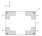
- FIG. 13 is a bottom view of the vibrator 22 in the piezoelectric vibration device 21.
- FIG. FIG. 14 is a plan view of the piezoelectric vibration device 21.
- FIG. 15 is a plan view of the substrate 31 in the piezoelectric vibration device 21.
- FIG. 16 is a cross-sectional view taken along line E in FIG. 15. FIG.
- specific descriptions of the same points as those of the already described embodiments will be omitted, and different parts will be mainly described.
- the piezoelectric vibration device 21 has a vibrator 22, an integrated circuit element 30, a substrate 31, and a mold portion (not shown).
- the vibrator 22 is a piezoelectric vibrator having a piezoelectric vibrating plate 23, a first sealing member 26, and a second sealing member 27.
- Vibrator 22 has a sandwich structure in which piezoelectric diaphragm 23 is sandwiched between first sealing member 26 and second sealing member 27 .
- the piezoelectric vibration plate 23 is a plate-like member made of crystal, which is a piezoelectric material.
- One principal surface and the other principal surface of the piezoelectric diaphragm 23 have a pair of excitation electrodes 24a.
- the pair of excitation electrodes 24 a are positioned so as to face each other in the thickness direction of the piezoelectric diaphragm 23 .
- the piezoelectric diaphragm 23 has a notch portion 24b penetrating from one main surface to the other main surface so as to surround the pair of excitation electrodes 24a when viewed in the Z direction, which is a plan view. .
- the notch portion 24b penetrates so as to surround the pair of excitation electrodes 24a with one portion left.
- the portion where the pair of excitation electrodes 24a are located is configured as a plate-like member having a cantilever structure. That is, the portion where the pair of excitation electrodes 24a are located is configured as the vibrating portion 24 capable of vibrating in the Z direction.
- the piezoelectric diaphragm 23 has a bonding material 25 on one main surface that is bonded to the first sealing member 26 so as to surround the vibrating portion 24 .
- the piezoelectric diaphragm 23 has a bonding material 25 bonded to the second sealing member so as to surround the vibrating portion 24 on the other main surface.
- the bonding material 25 is a PVD film made of the same metal as the metal forming the pair of excitation electrodes 24a.
- the first sealing member 26 is a member that seals the vibrating portion 24 of the piezoelectric diaphragm 23 .
- the first sealing member 26 is a plate-like member made of the same crystal as the piezoelectric diaphragm 23 .
- the first sealing member 26 has substantially the same shape as the piezoelectric diaphragm 23 . That is, when one main surface of the first sealing member 26 faces the one main surface of the piezoelectric diaphragm 23, the first sealing member 26 can cover the entire one main surface of the piezoelectric diaphragm 23 with the one main surface.
- the first sealing member 26 has a bonding material 25 to be bonded to the bonding material 25 of the piezoelectric diaphragm 23 on one main surface.
- the bonding material 25 of the first sealing member 26 is a PVD film made of the same metal as the bonding material 25 of the piezoelectric diaphragm 23 .
- the second sealing member 27 is a member that seals the vibrating portion 24 of the piezoelectric diaphragm 23 .
- the second sealing member 27 is a plate-like member made of the same crystal as the piezoelectric vibration plate 23 .
- the second sealing member 27 has substantially the same shape as the piezoelectric diaphragm 23 . That is, when one main surface of the second sealing member 27 faces the other main surface of the piezoelectric diaphragm 23, the one main surface of the second sealing member 27 can cover the entire other main surface of the piezoelectric diaphragm 23.
- the second sealing member 27 has a bonding material 25 that bonds with the bonding material 25 of the piezoelectric diaphragm 23 on one main surface.
- the bonding material 25 is a PVD film made of the same metal as the bonding material 25 .
- the second sealing member 27 has four vibrator mounting terminals 27 a electrically connected to the electrodes of the substrate 31 on the other main surface.
- the four transducer mounting terminals 27a are plate-like terminals made of conductive metal.
- the four transducer mounting terminals 27a are configured in a substantially L shape when viewed in the Z direction.
- a first sealing member 26 is located on one main surface of the piezoelectric diaphragm 23 .
- One main surface of the piezoelectric diaphragm 23 is covered with a first sealing member 26 .
- the bonding material 25 on one main surface of the piezoelectric diaphragm 23 and the bonding material 25 on the first sealing member 26 are diffusion-bonded.
- the excitation electrode 24 a on one main surface side of the piezoelectric diaphragm 23 is hermetically sealed by the first sealing member 26 .
- a second sealing member 27 is located on the other main surface of the piezoelectric diaphragm 23 .
- the other main surface of piezoelectric diaphragm 23 is covered with second sealing member 27 .
- the bonding material 25 on the other main surface of the piezoelectric diaphragm 23 and the bonding material 25 on the second sealing member 27 are diffusion-bonded.
- the excitation electrode 24 a on the other main surface side of the piezoelectric diaphragm 23 is hermetically sealed by the second sealing member 27 .
- the vibrator 22 configured in this manner is configured as a sandwich structure package in which both main surfaces of the piezoelectric diaphragm 23 are sealed with the first sealing member 26 and the second sealing member 27, respectively.
- the vibrator 22 has an internal structure including the vibrating portion 24 of the piezoelectric vibration plate 23. A space is formed. That is, the vibrator 22 has a vibrating portion 24 including a pair of excitation electrodes 24a hermetically sealed in the inner space of the package.
- the integrated circuit element 30 is an IC that controls the vibrator 22 . Since the configuration of the integrated circuit element 30 is the same as that of the integrated circuit element 10 of the first embodiment, description thereof is omitted.
- the substrate 31 is a member that electrically connects the vibrator 22 and the integrated circuit element 30 with a wiring pattern and integrally configures them.
- One of the pair of main surfaces of the substrate 31 is configured as a first mounting surface 31a having the wiring pattern including four connection terminals 31d made of a conductor such as copper, pads, lands, and the like. .
- the four connection terminals 31d are electrically connected to the wiring pattern including a plurality of pads on the first mounting surface 31a via internal wiring 31c.
- the vibrator 22 and the integrated circuit element 30 are mounted on the first mounting surface 31a of the substrate 31, respectively.
- the vibrator 22 is arranged on the substrate 31 with the second sealing member 27 facing the first mounting surface 31a (see FIG. 16).
- the four transducer mounting terminals 27a (see FIG. 13) of the second sealing member 27 are electrically connected to the four connection terminals 31d of the first mounting surface 31a by conductive solder H. (See FIG. 16).
- the integrated circuit element mounting terminals 30a of the integrated circuit element 30 are electrically connected to wiring patterns on the first mounting surface 31a of the substrate 31 by conductive solder H, respectively.
- the vibrator 22 and the integrated circuit element 30 are positioned side by side on the first mounting surface 31 a of the substrate 31 .
- the other main surface of the substrate 31 parallel to the one main surface is configured as a second mounting surface 31b having external connection terminals 31j for mounting on the external substrate P (see FIG. 9). It is
- the external connection terminal 31j is a plate-like terminal made of a conductive metal.
- the external connection terminal 31j is electrically connected to the wiring pattern including a plurality of pads on the first mounting surface 31a via internal wiring 31c (not shown).
- a mold portion (not shown) protects the substrate 31 and at least the oscillator 22 among the oscillator 22 and the integrated circuit element 30 mounted on the substrate 31 . Since the molded portion is the same as the molded portion 12 in the first embodiment, the explanation is omitted.
- FIG. 14 Note that the second mounting surface 31b of the substrate 31 is the same as the second mounting surface 11b of the substrate 11 in the first embodiment, so the description thereof is omitted.
- the first mounting surface 31a of the substrate 31 is one main surface electrically connected to the vibrator 22 and the integrated circuit element 30.
- the first mounting surface 31a has four recesses 31g (hereinafter simply referred to as "recesses 31g").
- the concave portion 31g is located so as to be line symmetrical in the X direction and the Y direction when viewed in the Z direction.
- each of the concave portions 31g is recessed in a direction perpendicular to the first mounting surface 31a in a substantially L-shaped range.
- the recess 31g has a bottom surface 31h parallel to the first mounting surface 31a and side surfaces 31i perpendicular to the first mounting surface 31a.
- the concave portion 31g has a shape in which the vibrator mounting terminals 27a of the vibrator 22 having one main surface facing the bottom surface 31h can be arranged therein.
- Approximately L-shaped connection terminals 31d are positioned in the recesses 31g. That is, the substrate 31 has four connection terminals 31d.
- the connection terminal 31d is a plate-like terminal made of a conductive metal.
- connection terminal 31d protrudes in the Z direction from the bottom surface 31h of each recess 31g.
- Main surfaces of the four connection terminals 31d (hereinafter simply referred to as "connection terminals 31d") perpendicular to the Z direction are formed as bonding surfaces 31e that are respectively bonded to the four transducer mounting terminals 27a of the transducer 22. .
- the connection terminal 31d is positioned in each recess 31g such that a predetermined gap G3 is formed from the side surface 31i of the bottom surface 31h.
- the joint surface 31 e is exposed without being covered with the insulating base material of the substrate 31 .
- a joint surface 31e of the connection terminal 31d is located closer to the bottom surface 31h than the first mounting surface 31a. That is, the joint surface 31e is recessed from the first mounting surface 31a.
- the connecting terminal 31d has an end surface 31f perpendicular to the bottom surface 31h of the recess 31g as an outer edge.
- the width X5 in the X direction of the two connection terminals 31d arranged in the X direction is wider than the width of the vibrator 22 in the X direction.
- the width Y5 in the Y direction of the two connection terminals 31d arranged in the Y direction is wider than the width of the vibrator 22 in the Y direction. That is, the connection terminal 31d extends in the X and Y directions from the outer edge of the vibrator 22 when viewed in the Z direction.
- An internal wiring 31c is connected to the connection terminal 31d.
- the internal wiring 31c is made of a conductive metal.
- the internal wiring 31c electrically connects the wiring pattern of the first mounting surface 31a and the external connection terminal 31j.
- the internal wiring 31c is connected to each connection terminal 31d inside the recess 31g. Further, the internal wiring 31c does not protrude beyond the joint surface 31e of the connection terminal 31d. Further, the internal wiring 31c is not covered with the base material of the substrate 31 inside the recess 31g. That is, the internal wiring 31c is exposed without being covered with the insulating base material of the substrate 31, like the connection terminal 31d.
- FIG. 14 the bonding between the vibrator 22 and the substrate 31 will be described with reference to FIGS. 14 and 16.
- each connection terminal 31d is positioned between the outer edge of the vibrator 22 and the side surface 31i.
- the four vibrator mounting terminals 27a of the vibrator 22 are joined by solder H applied to the four connection terminals 31d of the substrate 31, respectively.
- Each solder H is in close contact with the transducer mounting terminal 27a and in close contact with the connection terminal 31d.
- the solder H positioned between the vibrator mounting terminal 27a and the connection terminal 31d spreads toward the outer edge of the connection terminal 31d as the vibrator 22 and the substrate 31 approach each other.
- each solder H When each solder H reaches the outer edge of the connection terminal 31d, it spreads from the joint surface 31e toward the end surface 31f. Each solder H covers the joint surface 11e and the end surface 31f of the connection terminal 31d. That is, each solder H joins the vibrator mounting terminal 27a of the vibrator 22 with the bonding surface 31e and the end surface 31f.
- solder H adhered to the joint surface 31e of the connection terminal 31d spreads toward the internal wiring 31c connected to the connection terminal 31d.
- the solder H covers the internal wiring 31c in the connection terminal 31d.
- the solder H is joined while covering the internal wiring 31c of the connection terminal 31d.
- the vibrator 22 mounted on the substrate 31 includes four vibrator mounting terminals 27a to four connection terminals 31d on the first mounting surface 31a, a wiring pattern including a plurality of pads (not shown), internal wiring 31c, and the second mounting surface. It is electrically connected to an external substrate (not shown) via an external connection terminal 31j on 31b. Thereby, the vibrating portion 5 of the vibrator 22 oscillates at a predetermined frequency by the voltage applied from the external substrate.
- the piezoelectric vibrating device 21 configured in this manner includes a vibrator 22 having a sandwich structure in which each main surface of a piezoelectric vibrating plate 23 is sealed with a first sealing member 26 and a second sealing member 27 that are crystal plate materials. have. Therefore, the piezoelectric vibrating device 21 can have a lower overall height compared to a structure having a piezoelectric vibrator in which a box-shaped holding member made of ceramic or the like is sealed with a lid member.
- the piezoelectric vibration device 21 the vibrator 22 and the integrated circuit element 30 are mounted on the same first mounting surface 31 a of the substrate 31 . Therefore, the piezoelectric vibration device 21 can have a lower overall height than a configuration in which the vibrator 22 is mounted on the first mounting surface 31a of the substrate 31 and the integrated circuit element 30 is mounted on the second mounting surface 31b.
- the piezoelectric vibration device 21 has a molded portion (not shown) that covers at least one of the vibrator 22 and the integrated circuit element 30 together with the substrate 31 with resin, the vibrator 22 or the integrated circuit element 30 is protected from external shocks and vibrations. can protect at least one of In addition, since the substrate 31 has improved rigidity due to the molded portion, the connecting terminals 31d are less likely to bend due to impact and vibration. Therefore, in the piezoelectric vibrating device 21, strain generated in the joint surface 31e between the connection terminal 31d and the solder H due to external impact and vibration is suppressed.
- the solder H is bonded to the internal wiring 31c, the bonding surface 31e, and part of the end surface 31f of the connection terminal 31d, which is a protrusion projecting from the recess 31g.
- the bonding area with the connection terminal 31d is increased as compared with . Therefore, by bonding the vibrator 22 to the connecting terminal 31d, which is a projection, with the solder H, the vibrator 22 is more strongly bonded to the substrate 31 than when the vibrator mounting terminal 27a is bonded only to the bonding surface 31e. Thereby, the piezoelectric vibration device 21 can suppress separation between the vibrator 22 and the substrate 31 .
- the concave portion 11g of the substrate 11 is recessed in a range including part of the long side and part of the short side of the substrate 11, which is the outer edge of the substrate 11, when viewed in the Z direction.
- the concave portion of the substrate does not have to include the outer edge of the substrate.
- the recess may be recessed in an arbitrary shape in a portion that does not include the outer edge of the substrate when viewed in the Z direction.
- the substrate 11 has a recess 11g for each external connection terminal 11d.
- the substrate does not have to have a recess for each external connection terminal.
- a plurality of external connection terminals may be positioned in one concave portion of the substrate.
- a predetermined gap G is provided between each side surface 11i of the concave portion 11g of the substrate 11 and the end surfaces 11fa and 11fb of the adjacent external connection terminals 11d when viewed in the Z direction (see FIG. 6).
- the end face of the external connection terminal may be provided with a predetermined gap between the side face of the concave portion and the adjacent part of the end face when viewed in the Z direction.
- each recess 11g of the substrate 11 has the same thickness from the first mounting surface 11a to the bottom surface 11h.
- each concave portion of the substrate may have a different thickness from the first mounting surface to the bottom surface.
- the substrate 11 has four recesses 11g.
- the substrate only needs to have at least one recess.
- the four end surfaces 11f including the outer edges of the four external connection terminals 11d are arranged so that predetermined gaps G1 and G2 are formed inside the recess 11g from the outer edges of the bottom surface 11h when viewed in the Z direction. Located away from. However, the end surfaces including the outer edges of the four external connection terminals may be positioned apart from the outer edge of the bottom surface of the recess so that an arbitrary gap is formed inside the recess when viewed in the Z direction.
- each external connection terminal may have a plurality of internal wires exposed in the recess and electrically connected to a plurality of end surfaces of the external connection terminal.
- the vibrator 2 has a through hole 4c between the frame portion 4 and the vibrating portion 5, and supports the vibrating portion 5 in a cantilever manner.
- the vibrator may have a configuration that does not have a through hole between the frame portion and the vibrating portion.
- the substrate 11 is made of glass polyimide resin.
- the substrate may be a glass composite substrate such as a glass epoxy resin substrate, a fluororesin substrate, a ceramic substrate, or the like.
- the piezoelectric vibration device 1 has the vibrator 2 having a three-layer structure in which the piezoelectric vibration plate 3, the first sealing member 7, and the second sealing member 8 are laminated.
- the piezoelectric vibration device may have a vibrator with a three-layer structure or more.
- the vibrator may be a four-layer vibrator in which a sensor such as a thermistor is further mounted on the main surface of the first sealing member.
- the piezoelectric vibration device 1 has the vibration portions 5 and 17 positioned within the internal space S of the piezoelectric vibration plate 3 .
- the piezoelectric vibration device may be a so-called H-structured piezoelectric vibration device having a bottom and frame-shaped side walls extending in directions perpendicular to the two planes facing each other on the bottom.
- a piezoelectric element is positioned on one plane of the bottom portion and inside one of the side wall portions.
- an electronic component element is mounted on the other plane of the bottom portion and inside the other side wall portion.
- a first sealing member is joined to the tip of the one side wall, and a second sealing member is joined to the tip of the other side wall.
- the piezoelectric diaphragm 23 of the vibrator 22 has the vibrating portion 24 separated from the piezoelectric diaphragm 23 so as to surround the pair of excitation electrodes 24a with one part left. . That is, the vibrating portion 24 has a cantilever structure supported by the piezoelectric diaphragm 23 at one point. However, the vibrating portion may have a structure in which a piezoelectric diaphragm is supported at a plurality of locations.
- the vibrators 2 and 22 are joined to the substrates 11 and 31 by solder H.
- the vibrator only needs to be electrically and mechanically connected to the substrate.
- the vibrator may be bonded with, for example, a conductive adhesive or die attach tape.
Landscapes
- Physics & Mathematics (AREA)
- Acoustics & Sound (AREA)
- Piezo-Electric Or Mechanical Vibrators, Or Delay Or Filter Circuits (AREA)
- Oscillators With Electromechanical Resonators (AREA)
- Vibration Prevention Devices (AREA)
- Apparatuses For Generation Of Mechanical Vibrations (AREA)
Priority Applications (3)
| Application Number | Priority Date | Filing Date | Title |
|---|---|---|---|
| CN202280044249.5A CN117546406A (zh) | 2021-09-30 | 2022-08-31 | 压电振动器件 |
| JP2023550487A JP7747051B2 (ja) | 2021-09-30 | 2022-08-31 | 圧電振動デバイス |
| US18/696,562 US20240396521A1 (en) | 2021-09-30 | 2022-08-31 | Piezoelectric vibration device |
Applications Claiming Priority (2)
| Application Number | Priority Date | Filing Date | Title |
|---|---|---|---|
| JP2021-161145 | 2021-09-30 | ||
| JP2021161145 | 2021-09-30 |
Publications (1)
| Publication Number | Publication Date |
|---|---|
| WO2023053836A1 true WO2023053836A1 (ja) | 2023-04-06 |
Family
ID=85780613
Family Applications (1)
| Application Number | Title | Priority Date | Filing Date |
|---|---|---|---|
| PCT/JP2022/032821 Ceased WO2023053836A1 (ja) | 2021-09-30 | 2022-08-31 | 圧電振動デバイス |
Country Status (5)
| Country | Link |
|---|---|
| US (1) | US20240396521A1 (https=) |
| JP (1) | JP7747051B2 (https=) |
| CN (1) | CN117546406A (https=) |
| TW (1) | TWI824717B (https=) |
| WO (1) | WO2023053836A1 (https=) |
Citations (6)
| Publication number | Priority date | Publication date | Assignee | Title |
|---|---|---|---|---|
| JP2003229512A (ja) * | 2002-02-01 | 2003-08-15 | Nec Toppan Circuit Solutions Toyama Inc | 半導体チップ搭載用基板およびその製造方法と半導体装置およびその製造方法 |
| JP2005033755A (ja) * | 2002-12-10 | 2005-02-03 | Seiko Epson Corp | 圧電発振器およびその製造方法並びに電子機器 |
| JP2008277927A (ja) * | 2007-04-26 | 2008-11-13 | Nippon Dempa Kogyo Co Ltd | 表面実装用の圧電発振器 |
| JP2013176032A (ja) * | 2012-01-27 | 2013-09-05 | Daishinku Corp | 表面実装型圧電発振器 |
| JP2017200175A (ja) * | 2016-04-01 | 2017-11-02 | スカイワークスフィルターソリューションズジャパン株式会社 | 樹脂により画定された空洞を含む電子パッケージとその形成方法 |
| JP2018014705A (ja) * | 2016-07-07 | 2018-01-25 | 日本電波工業株式会社 | 恒温槽型水晶発振器 |
Family Cites Families (5)
| Publication number | Priority date | Publication date | Assignee | Title |
|---|---|---|---|---|
| JP4222147B2 (ja) * | 2002-10-23 | 2009-02-12 | セイコーエプソン株式会社 | 圧電発振器及び圧電発振器を利用した携帯電話装置および圧電発振器を利用した電子機器 |
| JP4811232B2 (ja) * | 2005-11-02 | 2011-11-09 | パナソニック株式会社 | 電子部品パッケージ |
| WO2009057699A1 (ja) * | 2007-10-30 | 2009-05-07 | Kyocera Corporation | 弾性波装置 |
| CN109716646A (zh) * | 2016-11-24 | 2019-05-03 | 株式会社大真空 | 压电振动器件以及具备其的sip模块 |
| JP6780718B2 (ja) * | 2019-02-28 | 2020-11-04 | 株式会社大真空 | 圧電振動デバイス |
-
2022
- 2022-08-31 CN CN202280044249.5A patent/CN117546406A/zh active Pending
- 2022-08-31 JP JP2023550487A patent/JP7747051B2/ja active Active
- 2022-08-31 US US18/696,562 patent/US20240396521A1/en active Pending
- 2022-08-31 WO PCT/JP2022/032821 patent/WO2023053836A1/ja not_active Ceased
- 2022-09-14 TW TW111134752A patent/TWI824717B/zh active
Patent Citations (6)
| Publication number | Priority date | Publication date | Assignee | Title |
|---|---|---|---|---|
| JP2003229512A (ja) * | 2002-02-01 | 2003-08-15 | Nec Toppan Circuit Solutions Toyama Inc | 半導体チップ搭載用基板およびその製造方法と半導体装置およびその製造方法 |
| JP2005033755A (ja) * | 2002-12-10 | 2005-02-03 | Seiko Epson Corp | 圧電発振器およびその製造方法並びに電子機器 |
| JP2008277927A (ja) * | 2007-04-26 | 2008-11-13 | Nippon Dempa Kogyo Co Ltd | 表面実装用の圧電発振器 |
| JP2013176032A (ja) * | 2012-01-27 | 2013-09-05 | Daishinku Corp | 表面実装型圧電発振器 |
| JP2017200175A (ja) * | 2016-04-01 | 2017-11-02 | スカイワークスフィルターソリューションズジャパン株式会社 | 樹脂により画定された空洞を含む電子パッケージとその形成方法 |
| JP2018014705A (ja) * | 2016-07-07 | 2018-01-25 | 日本電波工業株式会社 | 恒温槽型水晶発振器 |
Also Published As
| Publication number | Publication date |
|---|---|
| TWI824717B (zh) | 2023-12-01 |
| JP7747051B2 (ja) | 2025-10-01 |
| US20240396521A1 (en) | 2024-11-28 |
| TW202322426A (zh) | 2023-06-01 |
| JPWO2023053836A1 (https=) | 2023-04-06 |
| CN117546406A (zh) | 2024-02-09 |
Similar Documents
| Publication | Publication Date | Title |
|---|---|---|
| JP7196934B2 (ja) | 圧電振動デバイス | |
| US20110193644A1 (en) | Piezoelectric vibrator and oscillator using the same | |
| JP7683714B2 (ja) | 圧電振動デバイス | |
| JP7747051B2 (ja) | 圧電振動デバイス | |
| US20230155568A1 (en) | Vibrator device | |
| US12562708B2 (en) | Vibrator device | |
| JPWO2023048051A5 (https=) | ||
| JP6791772B2 (ja) | 水晶素子および水晶デバイス | |
| JP7300293B2 (ja) | 電子装置 | |
| CN110999079A (zh) | 压电振子 | |
| JP2019029857A (ja) | 水晶デバイス | |
| TWI894621B (zh) | 壓電振動裝置 | |
| TWI880326B (zh) | 壓電振動裝置 | |
| JP7538015B2 (ja) | 圧電共振デバイス | |
| JPWO2023053836A5 (https=) | ||
| JP7578903B2 (ja) | 発振器および製造方法 | |
| JP5123081B2 (ja) | 電子部品用の蓋体及び圧電振動子並びに圧電発振器 | |
| JP2023119714A (ja) | 振動デバイス | |
| JP2025163210A (ja) | 圧電共振デバイス | |
| JP5302733B2 (ja) | 圧電振動子及び圧電発振器 | |
| CN119545697A (zh) | 传感器元件以及物理量传感器 | |
| JP5468327B2 (ja) | 圧電デバイス | |
| CN120883505A (zh) | 压电振动器件 | |
| JP2013172356A (ja) | 表面実装型水晶発振器 | |
| JP2009118000A (ja) | 圧電デバイス |
Legal Events
| Date | Code | Title | Description |
|---|---|---|---|
| 121 | Ep: the epo has been informed by wipo that ep was designated in this application |
Ref document number: 22875708 Country of ref document: EP Kind code of ref document: A1 |
|
| WWE | Wipo information: entry into national phase |
Ref document number: 202280044249.5 Country of ref document: CN |
|
| WWE | Wipo information: entry into national phase |
Ref document number: 2023550487 Country of ref document: JP |
|
| WWE | Wipo information: entry into national phase |
Ref document number: 18696562 Country of ref document: US |
|
| NENP | Non-entry into the national phase |
Ref country code: DE |
|
| 122 | Ep: pct application non-entry in european phase |
Ref document number: 22875708 Country of ref document: EP Kind code of ref document: A1 |