WO2023042508A1 - 炭化珪素半導体装置 - Google Patents
炭化珪素半導体装置 Download PDFInfo
- Publication number
- WO2023042508A1 WO2023042508A1 PCT/JP2022/024785 JP2022024785W WO2023042508A1 WO 2023042508 A1 WO2023042508 A1 WO 2023042508A1 JP 2022024785 W JP2022024785 W JP 2022024785W WO 2023042508 A1 WO2023042508 A1 WO 2023042508A1
- Authority
- WO
- WIPO (PCT)
- Prior art keywords
- region
- gate
- contact hole
- main surface
- silicon carbide
- Prior art date
- Legal status (The legal status is an assumption and is not a legal conclusion. Google has not performed a legal analysis and makes no representation as to the accuracy of the status listed.)
- Ceased
Links
Images












Classifications
-
- H—ELECTRICITY
- H10—SEMICONDUCTOR DEVICES; ELECTRIC SOLID-STATE DEVICES NOT OTHERWISE PROVIDED FOR
- H10D—INORGANIC ELECTRIC SEMICONDUCTOR DEVICES
- H10D62/00—Semiconductor bodies, or regions thereof, of devices having potential barriers
- H10D62/80—Semiconductor bodies, or regions thereof, of devices having potential barriers characterised by the materials
- H10D62/81—Semiconductor bodies, or regions thereof, of devices having potential barriers characterised by the materials of structures exhibiting quantum-confinement effects, e.g. single quantum wells; of structures having periodic or quasi-periodic potential variation
-
- H—ELECTRICITY
- H10—SEMICONDUCTOR DEVICES; ELECTRIC SOLID-STATE DEVICES NOT OTHERWISE PROVIDED FOR
- H10W—GENERIC PACKAGES, INTERCONNECTIONS, CONNECTORS OR OTHER CONSTRUCTIONAL DETAILS OF DEVICES COVERED BY CLASS H10
- H10W20/00—Interconnections in chips, wafers or substrates
- H10W20/40—Interconnections external to wafers or substrates, e.g. back-end-of-line [BEOL] metallisations or vias connecting to gate electrodes
- H10W20/41—Interconnections external to wafers or substrates, e.g. back-end-of-line [BEOL] metallisations or vias connecting to gate electrodes characterised by their conductive parts
- H10W20/427—Power or ground buses
-
- H—ELECTRICITY
- H10—SEMICONDUCTOR DEVICES; ELECTRIC SOLID-STATE DEVICES NOT OTHERWISE PROVIDED FOR
- H10D—INORGANIC ELECTRIC SEMICONDUCTOR DEVICES
- H10D30/00—Field-effect transistors [FET]
- H10D30/60—Insulated-gate field-effect transistors [IGFET]
-
- H—ELECTRICITY
- H10—SEMICONDUCTOR DEVICES; ELECTRIC SOLID-STATE DEVICES NOT OTHERWISE PROVIDED FOR
- H10D—INORGANIC ELECTRIC SEMICONDUCTOR DEVICES
- H10D62/00—Semiconductor bodies, or regions thereof, of devices having potential barriers
- H10D62/10—Shapes, relative sizes or dispositions of the regions of the semiconductor bodies; Shapes of the semiconductor bodies
-
- H—ELECTRICITY
- H10—SEMICONDUCTOR DEVICES; ELECTRIC SOLID-STATE DEVICES NOT OTHERWISE PROVIDED FOR
- H10D—INORGANIC ELECTRIC SEMICONDUCTOR DEVICES
- H10D62/00—Semiconductor bodies, or regions thereof, of devices having potential barriers
- H10D62/10—Shapes, relative sizes or dispositions of the regions of the semiconductor bodies; Shapes of the semiconductor bodies
- H10D62/102—Constructional design considerations for preventing surface leakage or controlling electric field concentration
- H10D62/103—Constructional design considerations for preventing surface leakage or controlling electric field concentration for increasing or controlling the breakdown voltage of reverse-biased devices
- H10D62/105—Constructional design considerations for preventing surface leakage or controlling electric field concentration for increasing or controlling the breakdown voltage of reverse-biased devices by having particular doping profiles, shapes or arrangements of PN junctions; by having supplementary regions, e.g. junction termination extension [JTE]
- H10D62/106—Constructional design considerations for preventing surface leakage or controlling electric field concentration for increasing or controlling the breakdown voltage of reverse-biased devices by having particular doping profiles, shapes or arrangements of PN junctions; by having supplementary regions, e.g. junction termination extension [JTE] having supplementary regions doped oppositely to or in rectifying contact with regions of the semiconductor bodies, e.g. guard rings with PN or Schottky junctions
- H10D62/107—Buried supplementary regions, e.g. buried guard rings
-
- H—ELECTRICITY
- H10—SEMICONDUCTOR DEVICES; ELECTRIC SOLID-STATE DEVICES NOT OTHERWISE PROVIDED FOR
- H10D—INORGANIC ELECTRIC SEMICONDUCTOR DEVICES
- H10D64/00—Electrodes of devices having potential barriers
- H10D64/118—Electrodes comprising insulating layers having particular dielectric or electrostatic properties, e.g. having static charges
-
- H—ELECTRICITY
- H10—SEMICONDUCTOR DEVICES; ELECTRIC SOLID-STATE DEVICES NOT OTHERWISE PROVIDED FOR
- H10D—INORGANIC ELECTRIC SEMICONDUCTOR DEVICES
- H10D84/00—Integrated devices formed in or on semiconductor substrates that comprise only semiconducting layers, e.g. on Si wafers or on GaAs-on-Si wafers
- H10D84/80—Integrated devices formed in or on semiconductor substrates that comprise only semiconducting layers, e.g. on Si wafers or on GaAs-on-Si wafers characterised by the integration of at least one component covered by groups H10D12/00 or H10D30/00, e.g. integration of IGFETs
- H10D84/82—Integrated devices formed in or on semiconductor substrates that comprise only semiconducting layers, e.g. on Si wafers or on GaAs-on-Si wafers characterised by the integration of at least one component covered by groups H10D12/00 or H10D30/00, e.g. integration of IGFETs of only field-effect components
- H10D84/83—Integrated devices formed in or on semiconductor substrates that comprise only semiconducting layers, e.g. on Si wafers or on GaAs-on-Si wafers characterised by the integration of at least one component covered by groups H10D12/00 or H10D30/00, e.g. integration of IGFETs of only field-effect components of only insulated-gate FETs [IGFET]
-
- H—ELECTRICITY
- H10—SEMICONDUCTOR DEVICES; ELECTRIC SOLID-STATE DEVICES NOT OTHERWISE PROVIDED FOR
- H10D—INORGANIC ELECTRIC SEMICONDUCTOR DEVICES
- H10D30/00—Field-effect transistors [FET]
- H10D30/60—Insulated-gate field-effect transistors [IGFET]
- H10D30/64—Double-diffused metal-oxide semiconductor [DMOS] FETs
- H10D30/66—Vertical DMOS [VDMOS] FETs
- H10D30/668—Vertical DMOS [VDMOS] FETs having trench gate electrodes, e.g. UMOS transistors
-
- H—ELECTRICITY
- H10—SEMICONDUCTOR DEVICES; ELECTRIC SOLID-STATE DEVICES NOT OTHERWISE PROVIDED FOR
- H10D—INORGANIC ELECTRIC SEMICONDUCTOR DEVICES
- H10D62/00—Semiconductor bodies, or regions thereof, of devices having potential barriers
- H10D62/80—Semiconductor bodies, or regions thereof, of devices having potential barriers characterised by the materials
- H10D62/83—Semiconductor bodies, or regions thereof, of devices having potential barriers characterised by the materials being Group IV materials, e.g. B-doped Si or undoped Ge
- H10D62/832—Semiconductor bodies, or regions thereof, of devices having potential barriers characterised by the materials being Group IV materials, e.g. B-doped Si or undoped Ge being Group IV materials comprising two or more elements, e.g. SiGe
- H10D62/8325—Silicon carbide
-
- H—ELECTRICITY
- H10—SEMICONDUCTOR DEVICES; ELECTRIC SOLID-STATE DEVICES NOT OTHERWISE PROVIDED FOR
- H10D—INORGANIC ELECTRIC SEMICONDUCTOR DEVICES
- H10D64/00—Electrodes of devices having potential barriers
- H10D64/20—Electrodes characterised by their shapes, relative sizes or dispositions
- H10D64/27—Electrodes not carrying the current to be rectified, amplified, oscillated or switched, e.g. gates
- H10D64/311—Gate electrodes for field-effect devices
- H10D64/411—Gate electrodes for field-effect devices for FETs
- H10D64/511—Gate electrodes for field-effect devices for FETs for IGFETs
- H10D64/512—Disposition of the gate electrodes, e.g. buried gates
- H10D64/513—Disposition of the gate electrodes, e.g. buried gates within recesses in the substrate, e.g. trench gates, groove gates or buried gates
Definitions
- the present disclosure relates to silicon carbide semiconductor devices.
- Patent Document 1 A silicon carbide semiconductor device aimed at suppressing dielectric breakdown of an insulating film under a gate pad has been disclosed (for example, Patent Document 1).
- a silicon carbide semiconductor device of the present disclosure includes a silicon carbide substrate having a first main surface, an interlayer insulating film covering the first main surface, and a gate pad and a source pad provided on the interlayer insulating film.
- the silicon carbide substrate In plan view from a direction perpendicular to the first main surface, the silicon carbide substrate has a first region including a plurality of unit cells, a second region overlapping with the gate pad, and a second region in the second region.
- each of the plurality of unit cells includes a drift region having a first conductivity type; a body region having a second conductivity type different from the first conductivity type; a source region having the first conductivity type provided on the main surface and separated from the drift region by the body region; a source region provided on the first main surface and electrically connected to the body region; a contact region having a conductivity type; a gate electrode electrically connected to the gate pad; and a gate insulating film provided between the drift region, the body region and the source region, and the gate electrode.
- the second region has a first semiconductor region having the second conductivity type; the third region has a second semiconductor region having the second conductivity type; and the second semiconductor regions are connected to each other on the first main surface, and the interlayer insulating film has a first contact hole reaching the source region and the contact region, and a second contact hole reaching the second semiconductor region.
- the source pad is electrically connected to the source region and the contact region through the first contact hole, and is electrically connected to the second semiconductor region through the second contact hole.
- the second dimension in the width direction of the second contact hole is larger than the first dimension in the width direction of the first contact hole.
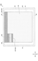
- FIG. 1 is a top view showing the silicon carbide semiconductor device according to the first embodiment.
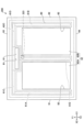
- FIG. 2 is a diagram showing respective regions within the silicon carbide substrate in the silicon carbide semiconductor device according to the first embodiment.
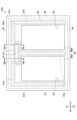
- FIG. 3 is a top view showing the region 221 in FIGS. 1 and 2 through the passivation film, the gate pad and the source pad.
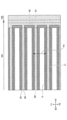
- FIG. 4 is a top view showing the configuration of the first main surface of the silicon carbide substrate in region 221 in FIGS. 1 and 2.
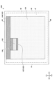
- FIG. FIG. 5 is a top view showing the region 222 in FIGS. 1 and 2 through the passivation film, gate pad and source pad.
- FIG. 6 is a top view showing the region 222 in FIGS. 1 and 2 through the passivation film, the gate pad and the source pad.
- FIG. 1 is a top view showing the silicon carbide semiconductor device according to the first embodiment.
- FIG. 2 is a diagram showing respective regions within the silicon carbide substrate in the silicon carbide semiconductor device according to the first embodiment.
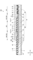
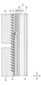
- FIG. 7 is a cross-sectional view showing the silicon carbide semiconductor device according to the first embodiment.
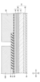
- FIG. 8 is a cross-sectional view showing the configuration of a unit cell.
- FIG. 9 is a cross-sectional view showing a silicon carbide semiconductor device according to a second embodiment.
- FIG. 10 is a top view showing a silicon carbide semiconductor device according to the third embodiment.
- FIG. 11 is a diagram showing respective regions in the silicon carbide substrate in the silicon carbide semiconductor device according to the third embodiment.
- FIG. 12 is a cross-sectional view (Part 1) showing the silicon carbide semiconductor device according to the third embodiment.
- FIG. 13 is a cross-sectional view (Part 2) showing the silicon carbide semiconductor device according to the third embodiment.
- FIG. 14 is a top view showing a silicon carbide semiconductor device according to a fourth embodiment.
- FIG. 15 is a diagram showing regions in a silicon carbide substrate in a silicon carbide semiconductor device according to a fourth embodiment.
- FIG. 16 is a cross-sectional view showing a silicon carbide semiconductor device according to a fourth embodiment.
- FIG. 17 is a top view showing the silicon carbide semiconductor device according to the fifth embodiment.
- FIG. 18 is a diagram showing respective regions in the silicon carbide substrate in the silicon carbide semiconductor device according to the fifth embodiment.
- FIG. 19 is a top view showing a silicon carbide semiconductor device according to the sixth embodiment.
- FIG. 20 is a diagram showing regions in a silicon carbide substrate in a silicon carbide semiconductor device according to the sixth embodiment.
- FIG. 21 is a top view showing a silicon carbide semiconductor device according to the seventh embodiment.
- FIG. 22 is a diagram showing respective regions in the silicon carbide substrate in the silicon carbide semiconductor device according to the seventh embodiment.
- FIG. 23 is a top view showing the silicon carbide semiconductor device according to the eighth embodiment.
- FIG. 24 is a top view showing the configuration of the first main surface of the silicon carbide substrate in region 223 in FIG. 23.
- FIG. 25 is a cross-sectional view (Part 1) showing the silicon carbide semiconductor device according to the eighth embodiment.
- FIG. 26 is a cross-sectional view (Part 2) showing the silicon carbide semiconductor device according to the eighth embodiment.
- FIG. 27 is a cross-sectional view (Part 3) showing the silicon carbide semiconductor device according to the eighth embodiment.
- FIG. 28 is a top view showing a modification of the first region.
- An object of the present disclosure is to provide a silicon carbide semiconductor device capable of alleviating electric field concentration in an interlayer insulating film.
- a silicon carbide semiconductor device includes a silicon carbide substrate having a first main surface, an interlayer insulating film covering the first main surface, and a gate provided on the interlayer insulating film.
- the silicon carbide substrate has a pad and a source pad, and the silicon carbide substrate includes a first region including a plurality of unit cells and a second region overlapping the gate pad when viewed from above in a direction perpendicular to the first main surface. and a third region connected to the second region, and each of the plurality of unit cells has a drift region having a first conductivity type and a second conductivity type different from the first conductivity type.
- a body region provided in the first main surface and separated from the drift region by the body region and having the first conductivity type; a source region provided in the first main surface and electrically connected to the body region; a contact region having the second conductivity type; a gate electrode electrically connected to the gate pad; and provided between the drift region, the body region and the source region, and the gate electrode. and a gate insulating film, wherein the second region has a first semiconductor region having the second conductivity type, and the third region has a second semiconductor region having the second conductivity type. and the first semiconductor region and the second semiconductor region are connected to each other on the first main surface, and a first contact hole reaching the source region and the contact region and the second semiconductor region are formed in the interlayer insulating film.
- the source pad is electrically connected to the source region and the contact region through the first contact hole, and the second semiconductor through the second contact hole.
- the second dimension in the widthwise direction of the second contact hole is the first dimension in the widthwise direction of the first contact hole. Larger than the dimensions.
- a third region is provided that is contiguous with the second region, and the first semiconductor region and the second semiconductor region are contiguous on the first main surface. Further, in a cross-sectional view from a direction parallel to the first main surface, the second dimension in the short direction of the second contact hole is larger than the first dimension in the short direction of the first contact hole. Therefore, the contact resistance between the source pad and the second semiconductor region is reduced, and even if a surge occurs, electric field concentration on the interlayer insulating film in the second region can be alleviated.
- the contact region and the second semiconductor region may be connected to each other on the first main surface. In this case, it is easy to control the contact region and the second semiconductor region to have the same potential.
- an active region including the plurality of unit cells and a termination region provided around the active region, the termination region being of the second conductivity type , wherein the second semiconductor region is provided between the gate pad and the termination region in plan view from a direction perpendicular to the first main surface, and the first main surface a fourth semiconductor region contiguous to the first semiconductor region and the third semiconductor region in a plane, wherein the concentration of the impurity of the second conductivity type in the third semiconductor region is equal to the second conductivity type in the fourth semiconductor region; and the second contact hole may include a third contact hole reaching the fourth semiconductor region.
- electric field concentration on the interlayer insulating film in the vicinity of the termination region can be alleviated.
- a field insulating film is provided between the first semiconductor region, the fourth semiconductor region, the third semiconductor region, and the interlayer insulating film, and the field insulating film includes: A fourth contact hole reaching the fourth semiconductor region is formed, the interlayer insulating film is in contact with the fourth semiconductor region inside the fourth contact hole, and the third contact hole is inside the fourth contact hole. may be located in In this case, the electric field concentration in the interlayer insulating film can be alleviated.
- a source runner electrically connected to the source pad and electrically connected to the fourth semiconductor region through the third contact hole;
- the side surface of the source runner on the side away from the gate pad is on the boundary line between the third semiconductor region and the fourth semiconductor region, or above the boundary line. It may be located close to the gate pad. In this case, electric field concentration in the interlayer insulating film under the source runner can be easily alleviated.
- the fourth semiconductor region is provided between the first gate runner and the second gate runner in plan view from a direction perpendicular to the first main surface, and A fifth semiconductor region connected to the first semiconductor region in a plane may be included, and the second contact hole may include a fifth contact hole reaching the fifth semiconductor region. In this case, the contact resistance between the source pad and the fourth semiconductor region can be further reduced in the vicinity of the gate pad.
- the fourth semiconductor region is provided between the gate pad and the third gate runner in plan view from a direction perpendicular to the first main surface,
- a sixth semiconductor region connected to the first semiconductor region on one main surface may be included, and the second contact hole may include a sixth contact hole reaching the sixth semiconductor region.
- the degree of freedom in arranging the gate pads can be increased.
- the plurality of unit cells extend in a first direction parallel to the first main surface and are arranged side by side in a second direction perpendicular to the first direction.
- the gate pad has a rectangular planar shape with the first direction as a longitudinal direction when viewed from above in a direction perpendicular to the first main surface, and the second semiconductor region has the second semiconductor region.
- a seventh semiconductor region provided at a position sandwiching the gate pad between the fourth semiconductor region and the fourth semiconductor region in a direction may be included, and the second contact hole may include a seventh contact hole reaching the seventh semiconductor region. In this case, contact resistance between the source pad and the second semiconductor region can be further reduced.
- the third dimension in the widthwise direction of the third contact hole is the fourth dimension in the widthwise direction of the seventh contact hole. may be equal to the dimension. In this case, the current generated in the first semiconductor region tends to flow evenly toward the third contact hole and the seventh contact hole.
- a fifth dimension in the first direction of the third contact hole may be larger than a sixth dimension in the first direction of the gate pad. In this case, it is easier to reduce the contact resistance.
- the silicon carbide substrate has a first side and a second side parallel to each other and a side perpendicular to the first side and the second side.
- a fourth gate runner extending along the first side, a fifth gate runner extending along the second side, and the fourth gate having a rectangular shape with a third side and a fourth side.
- a sixth gate runner extending from the gate pad toward the fourth side between the runner and the fifth gate runner, wherein the fourth gate runner, the fifth gate runner and the sixth gate;
- a runner may be electrically connected to the gate pad. In this case, it is easy to evenly apply the gate voltage to each unit cell from the fourth, fifth, and sixth gate runners.
- the seventh dimension in the first direction of the portion of the seventh contact hole between the fourth gate runner and the sixth gate runner in plan view is equal to the fourth gate runner and the sixth gate runner.
- the dimension in the first direction of the unit cell arranged on the extension line of the seventh contact hole in the portion between the fourth gate runner and the sixth gate runner is between the fourth gate runner and the sixth gate runner. 1/2 or less of the distance of Therefore, it is easy to apply a gate voltage to this unit cell in the same manner as other unit cells.
- the eighth dimension in the first direction of the portion between the fifth gate runner and the sixth gate runner in plan view of the seventh contact hole is It may be 1/2 or more of the distance between the fifth gate runner and the sixth gate runner.
- the dimension in the first direction of the unit cell arranged on the extension line of the seventh contact hole in the portion between the fifth gate runner and the sixth gate runner is between the fifth gate runner and the sixth gate runner. 1/2 or less of the distance of Therefore, it is easy to apply a gate voltage to this unit cell in the same manner as other unit cells.
- a plane including the X1-X2 direction and the Y1-Y2 direction is referred to as the XY plane
- a plane including the Y1-Y2 direction and the Z1-Z2 direction is referred to as the YZ plane
- a plane including the Z1-Z2 direction and the X1-X2 direction. is described as the ZX plane.
- the Z1-Z2 direction is the vertical direction
- the Z1 side is the upper side
- the Z2 side is the lower side.
- the term "planar view” refers to viewing the object from the Z1 side
- the term "planar shape” refers to the shape of the object viewed from the Z1 side.
- FIG. 1 is a top view showing the silicon carbide semiconductor device according to the first embodiment.
- FIG. 2 is a diagram showing respective regions within the silicon carbide substrate in the silicon carbide semiconductor device according to the first embodiment.
- FIG. 3 is a top view showing the region 221 in FIGS. 1 and 2 through the passivation film, the gate pad and the source pad.
- FIG. 4 is a top view showing the configuration of the first main surface of the silicon carbide substrate in region 221 in FIG.
- FIG. 5 is a top view showing the region 222 in FIG. 2 through the passivation film, the gate pad and the source pad.
- FIG. 1 is a top view showing the silicon carbide semiconductor device according to the first embodiment.
- FIG. 2 is a diagram showing respective regions within the silicon carbide substrate in the silicon carbide semiconductor device according to the first embodiment.
- FIG. 3 is a top view showing the region 221 in FIGS. 1 and 2 through the passivation film, the gate pad and the source pad.
- FIG. 4 is a top
- FIG. 6 is a top view showing the region 222 in FIG. 2 through the passivation film, the gate pad and the source pad.
- FIG. 7 is a cross-sectional view showing the silicon carbide semiconductor device according to the first embodiment.
- FIG. 7 corresponds to a cross-sectional view taken along line VII-VII in FIGS. 1 and 2.
- FIG. FIG. 8 is a cross-sectional view showing the configuration of a unit cell. 7 and 8, the passivation film is omitted.
- a MOSFET 201 includes a silicon carbide substrate 10, a gate insulating film 63, a gate electrode 51, an interlayer insulating film 44, a contact electrode 52, and a passivation film 80. , and a drain electrode 53 .
- the MOSFET 201 further includes a gate pad 61, a source pad 62, a gate runner (gate wiring) 61A, a gate runner 61B, a gate runner 61C, a gate runner 61D, a gate runner 61E, and a source runner (source wiring). 62C.
- Silicon carbide substrate 10 includes a silicon carbide single crystal substrate 20 and a silicon carbide epitaxial layer 30 on silicon carbide single crystal substrate 20 .
- Silicon carbide substrate 10 has a first main surface 1 and a second main surface 2 opposite to first main surface 1 .
- Silicon carbide epitaxial layer 30 forms first main surface 1
- silicon carbide single-crystal substrate 20 forms second main surface 2 .
- Silicon carbide single-crystal substrate 20 and silicon carbide epitaxial layer 30 are made of, for example, polytype 4H hexagonal silicon carbide.
- Silicon carbide single-crystal substrate 20 contains an n-type impurity such as nitrogen (N) and has n-type (first conductivity type).
- the first main surface 1 is a plane in which the ⁇ 0001 ⁇ plane or the ⁇ 0001 ⁇ plane is inclined in the off direction by an off angle of 8° or less.
- the first main surface 1 is the (000-1) plane or a plane in which the (000-1) plane is inclined in the off direction by an off angle of 8° or less.
- the off direction may be, for example, the ⁇ 11-20> direction or the ⁇ 1-100> direction.
- the off angle may be, for example, 1° or more, or may be 2° or more.
- the off angle may be 6° or less, or may be 4° or less.
- silicon carbide substrate 10 has a rectangular shape with first side 91 and second side 92 parallel to each other, and third side 93 and fourth side 94 perpendicular to first side 91 and second side 92 .
- has the shape of The first side 91 and the second side 92 are parallel to the Y1-Y2 direction, and the third side 93 and the fourth side 94 are parallel to the X1-X2 direction.
- the first side 91 is on the X2 side of the second side 92
- the second side 92 is on the X1 side of the first side 91 .
- the third side 93 is on the Y1 side of the fourth side 94
- the fourth side 94 is on the Y2 side of the third side 93 .
- the silicon carbide substrate 10 has an active region 41 and a termination region 42 provided around the active region 41 in plan view.
- the active region 41 has a first region 101 , a second region 102 and a third region 103 .
- a first area 101 is an area in which a plurality of unit cells 40 are arranged.
- the second region 102 is a region that overlaps the gate pad 61 in plan view.
- the unit cells 40 are arranged in the Y1-Y2 direction with the X1-X2 direction as the longitudinal direction. The dimensions in the Y1-Y2 direction of each unit cell 40 are common.
- Each unit cell 40 has a pair of gate trenches and gate electrodes.
- the unit cells 40 are arranged at a constant pitch P1 in the Y1-Y2 direction.
- the X1-X2 direction is an example of the first direction
- the Y1-Y2 direction is an example of the second direction.
- the silicon carbide epitaxial layer 30 includes a drift region 31, a body region 32, a source region 33, a contact region 34, a buried region 35, a buried junction termination extension (JTE) region 36, a surface It mainly has a JTE region 37 .
- Drift region 31 is provided over active region 41 and termination region 42 .
- Body region 32 , source region 33 , contact region 34 and buried region 35 are provided within active region 41 .
- Buried JTE region 36 and surface JTE region 37 are provided in termination region 42 .
- a portion of the contact region 34 and the buried region 35 may also be provided in the termination region 42 .
- Drift region 31 is provided on silicon carbide single crystal substrate 20 .
- Drift region 31 is located closer to first main surface 1 than silicon carbide single-crystal substrate 20 is.
- Drift region 31 may continue to silicon carbide single-crystal substrate 20 .
- Drift region 31 contains n-type impurities such as nitrogen or phosphorus (P), and has n-type conductivity.
- the body region 32 is provided on the drift region 31.
- Body region 32 contains a p-type impurity such as aluminum (Al) and has a p-type conductivity (second conductivity type).
- Body region 32 is located closer to first main surface 1 than drift region 31 is.
- Drift region 31 is located closer to second main surface 2 than body region 32 .
- Body region 32 is in contact with drift region 31 .
- a source region 33 is provided on the body region 32 .
- Source region 33 is separated from drift region 31 by body region 32 .
- the source region 33 contains an n-type impurity such as nitrogen or phosphorus and has n-type conductivity.
- Source region 33 is located closer to first main surface 1 than body region 32 is.
- Body region 32 is located closer to second main surface 2 than source region 33 is.
- Source region 33 is in contact with body region 32 .
- Source region 33 constitutes first main surface 1 .
- Source region 33 is covered with gate insulating film 43 .
- Source region 33 is in direct contact with gate insulating film 43 .
- the contact region 34 contains p-type impurities such as aluminum and has p-type conductivity.
- the p-type impurity concentration of the contact region 34 is higher than the p-type impurity concentration of the body region 32, for example.
- Contact region 34 penetrates source region 33 and body region 32 .
- Contact region 34 contacts body region 32 .
- Contact region 34 constitutes first main surface 1 .
- a gate trench 5 defined by the side surface 3 and the bottom surface 4 is provided on the first main surface 1 .
- Side surface 3 reaches drift region 31 through source region 33 and body region 32 .
- the bottom surface 4 is continuous with the side surfaces 3 .
- a source region 33 , a body region 32 and a drift region 31 are in contact with the side surface 3 .
- Bottom surface 4 is located in drift region 31 .
- the bottom surface 4 is, for example, a plane parallel to the second main surface 2 .
- An angle ⁇ 1 of the side surface 3 with respect to the plane including the bottom surface 4 is, for example, 45° or more and 65° or less.
- the angle ⁇ 1 may be, for example, 50° or more.
- the angle ⁇ 1 may be, for example, 60° or less.
- Side 3 preferably has a ⁇ 0-33-8 ⁇ plane.
- the ⁇ 0-33-8 ⁇ plane is a crystal plane that provides excellent mobility.
- the gate trench 5 extends in the X1-X2 direction parallel to the first main surface 1 in plan view. Also, in plan view, a plurality of gate trenches 5 are provided at regular intervals in the Y1-Y2 direction. Gate trenches 5 are not provided in the second region 102 and the third region 103 .
- the embedded region 35 contains a p-type impurity such as aluminum and has a p-type conductivity. Embedded region 35 is located closer to second main surface 2 than contact region 34 . Contact region 34 is located closer to first main surface 1 than buried region 35 . Buried region 35 is in contact with contact region 34 . Embedded region 35 is formed at a position deeper than gate trench 5 . The top surface of embedded region 35 is positioned closer to second main surface 2 than bottom surface 4 of gate trench 5 .
- the embedded JTE region 36 contacts the embedded region 35 in a direction parallel to the first main surface 1 .
- the embedded JTE region 36 is formed in an annular shape in plan view. Buried JTE region 36 contains p-type impurities, such as aluminum, and has p-type conductivity.
- the embedded JTE region 36 is spaced from the first major surface 1 and the second major surface 2 .
- the upper end surface of embedded JTE region 36 contacts the lower end surface of contact region 34 .
- the surface JTE region 37 contacts the contact region 34 in a direction parallel to the first main surface 1 .
- the surface JTE region 37 is formed in an annular shape in plan view.
- Surface JTE region 37 contains p-type impurities such as aluminum and has p-type conductivity.
- Surface JTE region 37 is provided above buried JTE region 36 .
- Surface JTE region 37 is spaced from buried JTE region 36 .
- Surface JTE region 37 is located closer to first main surface 1 than buried JTE region 36 .
- Embedded JTE region 36 is located closer to second main surface 2 than surface JTE region 37 .
- Surface JTE region 37 constitutes first main surface 1 .
- a portion of drift region 31 is between surface JTE region 37 and buried JTE region 36 .
- the concentration of p-type impurities in surface JTE region 37 is lower than the concentration of p-type impurities in contact region 34 .
- Surface JTE region 37 is an example of third semiconductor region 113 .
- the gate insulating film 43 is, for example, an oxide film.
- the gate insulating film 43 is made of a material containing silicon dioxide, for example.
- the gate insulating film 43 is in contact with the side surfaces 3 and the bottom surface 4 .
- Gate insulating film 43 is in contact with drift region 31 at bottom surface 4 .
- Gate insulating film 43 is in contact with each of source region 33 , body region 32 and drift region 31 at side surface 3 .
- Gate insulating film 43 may be in contact with source region 33 , contact region 34 and surface JTE region 37 on first main surface 1 .
- the gate electrode 51 is provided on the gate insulating film 43 .
- the gate electrode 51 is made of, for example, polysilicon (poly-Si) containing conductive impurities. A portion of the gate electrode 51 is arranged inside the gate trench 5 . A portion of gate electrode 51 is arranged above first main surface 1 .
- the interlayer insulating film 44 is provided in contact with the gate electrode 51 and the gate insulating film 43 .
- the interlayer insulating film 44 is, for example, an oxide film.
- the interlayer insulating film 44 is made of a material containing silicon dioxide, for example.
- the interlayer insulating film 44 electrically insulates the gate electrode 51 from the contact electrode 52 and the source pad 62 .
- a contact hole 70 for a gate is formed in the interlayer insulating film 44 .
- Gate electrode 51 is exposed from interlayer insulating film 44 through contact hole 70 .
- the gate pad 61 is provided on the interlayer insulating film 44 and is in contact with the gate electrode 51 within the contact hole 70 .
- the gate pad 61 is made of a material containing aluminum, for example.
- a source contact hole 71 is formed in the interlayer insulating film 44 and the gate insulating film 43 .
- the source region 33 and the contact region 34 in the first region 101 are exposed from the interlayer insulating film 44 and the gate insulating film 43 through the contact hole 71 .
- Contact hole 71 is an example of a first contact hole.
- a contact hole 72 is formed in the interlayer insulating film 44 and the gate insulating film 43 .
- the contact region 34 in the third region 103 is exposed from the interlayer insulating film 44 and the gate insulating film 43 through the contact hole 72 .
- a portion of source region 33 may be exposed through contact hole 72 .
- the widthwise dimension W2 of the contact hole 72 is larger than the widthwise dimension W1 of the contact hole 71 .
- the dimension W1 is the dimension of the contact hole 71 in the Y1-Y2 direction
- the dimension W2 is the dimension of the contact hole 72 in the Y1-Y2 direction.
- Contact hole 72 is an example of a second contact hole.
- the dimension W1 is an example of a first dimension
- the dimension W2 is an example of a second dimension.
- the contact electrode 52 is in contact with the source region 33 and the contact region 34 within the contact hole 71 .
- the contact electrode 52 is made of a material containing nickel silicide (NiSi), for example.
- Contact electrode 52 may be made of a material containing titanium, aluminum, and silicon.
- the contact electrode 52 is in ohmic contact with the source region 33 and contact region 34 .
- the source pad 62 is provided on the interlayer insulating film 44 and is in contact with the contact electrode 52 within the contact hole 71 .
- the source pad 62 is made of a material containing aluminum, for example.
- Source pad 62 may include a barrier metal film (not shown) covering the surface of interlayer insulating film 44 .
- source pads 62 may include source pads 62A and 62B.
- source pad 62A is on the X2 side of the center of silicon carbide substrate 10 in the X1-X2 direction
- source pad 62B is on the X1 side of the center of silicon carbide substrate 10 in the X1-X2 direction.
- the gate pad 61 is located on the Y1 side of the source pad 62, and the planar shape of the gate pad 61 is rectangular.
- the dimension of the gate pad 61 in the X1-X2 direction is larger than the dimension in the Y1-Y2 direction.
- the source pad 62 is located on the Y2 side of the gate pad 61 and has a rectangular planar shape.
- the distance of the gate pad 61 from the first side 91 and the distance from the second side 92 are approximately the same.
- the distance of gate pad 61 from third side 93 is smaller than the distance from fourth side 94 .
- the distance of the source pad 62 from the first side 91 and the distance from the second side 92 are approximately the same.
- the distance of source pad 62 from third side 93 is greater than the distance from fourth side 94 .
- the dimension in the X1-X2 direction of the gate pad 61 may be smaller than the dimension in the X1-X2 direction of the source pad 62, and the dimension in the Y1-Y2 direction of the gate pad 61 may be smaller than the dimension in the Y1-Y2 direction of the source pad 62.
- Source pad 62 is arranged so as to include a center line that bisects silicon carbide substrate 10 in the Y1-Y2 direction in plan view.
- the gate runner 61A extends along the first side 91 in the Y1-Y2 direction.
- the gate runner 61B extends along the second side 92 in the Y1-Y2 direction.
- Gate runners 61C and 61D are connected to gate pad 61 .
- Gate runners 61C and 61D extend along the third side 93 in the X1-X2 direction.
- the gate runner 61C is on the X2 side of the gate pad 61, and the gate runner 61D is on the X1 side of the gate pad 61.
- the Y1 side end of the gate runner 61A and the X2 side end of the gate runner 61C are connected.
- gate runner 61A is on the X2 side of source pad 62A
- gate runner 61B is on the X1 side of source pad 62B.
- the gate pad 61 is continuous with the gate runners 61C and 61D
- the gate runner 61A is continuous with the gate runner 61C
- the gate runner 61B is continuous with the gate runner 61D.
- Gate runners 61A and 61B are spaced apart from gate pad 61 in the X1-X2 direction.
- the gate runner 61E is connected to the gate pad 61 and extends in the Y1-Y2 direction between the source pads 62A and 62B.
- Gate runners 61 A, 61 B, 61 C, 61 D and 61 E are made of the same material as gate pad 61 .
- Gate runner 61C is an example of a first gate runner
- gate runner 61D is an example of a second gate runner.
- Gate runner 61A is an example of a fourth gate runner
- gate runner 61B is an example of a fifth gate runner
- gate runner 61E is an example of a sixth gate runner.
- the source runner 62C is annularly provided outside the source pad 62 and the gate runners 61A, 61B, 61C and 61D in plan view.
- Source runner 62C is connected to source pad 62 and is continuous.
- Source runner 62C is made of the same material as source pad 62.
- a contact hole for the source runner 62C is annularly formed in the interlayer insulating film 44 and the gate insulating film 43, and the source runner 62C is electrically connected to the contact region 34 through the annular contact hole.
- the side surface 64 of the source runner 62C on the side away from the gate pad 61 is on the boundary line between the contact region 34 and the surface JTE region 37, or the gate is located above this boundary line. It is preferably located near the pad 61 . This is because electric field concentration on the interlayer insulating film 44 under the source runner 62C is easily alleviated.
- a passivation film 80 covers the gate pad 61 , source pad 62 and interlayer insulating film 44 .
- the passivation film 80 is in contact with the gate pad 61 , the source pad 62 and the interlayer insulating film 44 .
- the passivation film 80 also covers the gate runners 61A, 61B, 61C, 61D and 61E and the source runner 62C.
- the passivation film 80 is also in contact with the gate runners 61A, 61B, 61C, 61D and 61E and the source runner 62C.
- the passivation film 80 is made of a material containing, for example, silicon nitride or polyimide.
- the passivation film 80 is formed with an opening 81 exposing a portion of the upper surface of the gate pad 61 and an opening 82 exposing a portion of the upper surface of the source pad 62 .
- the drain electrode 53 is in contact with the second main surface 2 . Drain electrode 53 is in contact with silicon carbide single-crystal substrate 20 at second main surface 2 . Drain electrode 53 is electrically connected to drift region 31 .
- the drain electrode 53 is made of a material containing nickel silicide, for example. Drain electrode 53 may be made of a material containing titanium, aluminum, and silicon. Drain electrode 53 is in ohmic contact with silicon carbide single crystal substrate 20 .
- a buffer layer containing an n-type impurity such as nitrogen and having n-type conductivity may be provided between silicon carbide single-crystal substrate 20 and drift region 31 .
- the second region 102 is on the Z2 side of the gate pad 61.
- the third area 103 continues to the second area 102 .
- the third area 103 has a fourth area 104 and a seventh area 107 .
- the fourth region 104 is located on the Z2 side of the gate runner 61C, the Z2 side of the gate runner 61D, and the Y1 side of the gate pad 61, the gate runner 61C, and the gate runner 61D in plan view.
- the seventh region 107 is on the Y2 side of the gate pad 61 in plan view.
- the first region 101 is on the Y2 side of the seventh region 107 and on the Y2 side of the gate runners 61C and 61D in plan view.
- the first region 101 is provided in the X1-X2 direction from the vicinity of the gate runner 61A to the vicinity of the gate runner 61B.
- the gate trench 5 is provided in the first region 101 but not provided in the second region 102 and the third region 103 .
- a source region 33 is also provided in the first region 101 but not provided in the second region 102 and the third region 103 . Therefore, in the second region 102 and the third region 103 , the first main surface 1 is formed by the contact regions 34 .
- Contact region 34 in first region 101 , contact region 34 in second region 102 , and contact region 34 in third region 103 are connected to each other on first main surface 1 .
- the source regions 33 are provided between the gate trenches 5 adjacent in the Y1-Y2 direction.
- Each unit cell 40 includes a pair of gate trenches 5 and gate electrodes 51, and a plurality of unit cells 40 are arranged in the Y1-Y2 direction at a constant pitch P1 in the first region 101.
- FIG. The contact region 34 within the second region 102 is an example of the first semiconductor region 111
- the contact region 34 within the third region 103 is an example of the second semiconductor region 112 .
- the contact region 34 within the fourth region 104 is an example of the fourth semiconductor region 114
- the contact region 34 within the seventh region 107 is an example of the seventh semiconductor region 117 .
- the source contact holes 71 formed in the interlayer insulating film 44 are arranged at a constant pitch P2 equal to the pitch P1 in the Y1-Y2 direction.
- the contact hole 70 for the gate is formed in the interlayer insulating film 44, but the contact holes 71 and 72 are not formed. Gate contact holes 70 are also formed in the interlayer insulating film 44 between the gate runners 61 A, 61 B, 61 C, 61 D and 61 E and the gate electrode 51 .
- the contact hole 72 includes a contact hole 73 reaching the contact region 34 in the fourth region 104 and a contact hole 77 reaching the contact region 34 in the seventh region 107.
- the widthwise dimension W3 of the contact hole 73 and the widthwise dimension W7 of the contact hole 77 are larger than the widthwise dimension W1 of the contact hole 71. big.
- the dimension W3 is the dimension of the contact hole 73 in the Y1-Y2 direction
- the dimension W7 is the dimension of the contact hole 77 in the Y1-Y2 direction. Dimension W3 and dimension W7 may be equal.
- the contact hole 73 is an example of a third contact hole, and the contact hole 77 is an example of a seventh contact hole.
- the dimension W3 is an example of a third dimension, and the dimension W7 is an example of a fourth dimension.
- Contact hole 73 is part of the contact hole for source runner 62C.
- the contact electrode 52 is in contact with the contact region 34 within the contact hole 73 and the contact hole 77 .
- the contact electrode 52 is in ohmic contact with the contact region 34 .
- the source pad 62 is in contact with the contact electrode 52 even inside the contact hole 77 .
- the source runner 62 ⁇ /b>C is in contact with the contact electrode 52 within the contact hole 73 .
- a third region 103 is provided which is continuous with the second region 102 , and the contact regions 34 are continuous in the second region 102 and the third region 103 . Further, in a cross-sectional view from a direction parallel to the first main surface 1 , the widthwise dimension W2 of the contact hole 72 is larger than the widthwise dimension W1 of the contact hole 71 . Therefore, the contact resistance between the source pad 62 and the contact region 34 is reduced, and even if a surge occurs, electric field concentration on the interlayer insulating film 44 in the second region 102 can be alleviated.
- the contact region 34 is in contact with the surface JTE region 37, even when a large voltage is applied between the drain electrode 53 and the source runner 62C, the interlayer insulating film 44 below the source runner 62C is It is possible to relax the electric field concentration on the
- the third area 103 includes the fourth area 104 and the seventh area 107 .
- the third region 103 may include only one of the fourth region 104 and the seventh region 107, including both the fourth region 104 and the seventh region 107 allows a Contact resistance can be further reduced.
- the widthwise dimension W3 of the contact hole 73 and the widthwise dimension W7 of the contact hole 77 are equal, the current generated in the contact region 34 in the second region 102 flows into the contact hole 73 and the contact hole 77. It tends to flow evenly toward the
- the gate runners 61A, 61B and 61E extending in the Y1-Y2 direction are provided, it is easy to evenly apply the gate voltage to each unit cell 40 from the gate runners 61A, 61B and 61E.
- the contact region 34 in the first region 101 and the contact region 34 in the third region 103 are connected to each other, it is easy to control them to have the same potential.
- the dimension L1 of the contact hole 73 in the X1-X2 direction is preferably larger than the dimension L2 of the gate pad 61 in the X1-X2 direction. This is because the contact resistance in the fourth region 104 can be more easily reduced.
- the dimension L1 is an example of a fifth dimension
- the dimension L2 is an example of a sixth dimension.
- the dimension L3 in the X1-X2 direction of the portion of the contact hole 77 between the gate runners 61A and 61E in plan view is 1/2 or more of the distance between the gate runners 61A and 61E.
- the dimension in the X1-X2 direction of the unit cell 40 arranged on the extension line of the contact hole 77 in the portion between the gate runners 61A and 61E is the distance between the gate runners 61A and 61E. 1/2 or less. Therefore, it is easy to apply a gate voltage to this unit cell 40 in the same manner as other unit cells 40 .
- Dimension L3 is an example of a seventh dimension.
- the dimension L4 in the X1-X2 direction of the portion of the contact hole 77 between the gate runners 61B and 61E in plan view is 1/2 or more of the distance between the gate runners 61B and 61E. is preferably In this case, the dimension in the X1-X2 direction of the unit cell 40 arranged on the extension line of the contact hole 77 in the portion between the gate runners 61B and 61E is the distance between the gate runners 61B and 61E. 1/2 or less. Therefore, it is easy to apply a gate voltage to this unit cell 40 in the same manner as other unit cells 40 .
- Dimension L4 is an example of an eighth dimension.
- FIG. 9 is a cross-sectional view showing a silicon carbide semiconductor device according to a second embodiment.
- FIG. 9, like FIG. 7, corresponds to a cross-sectional view taken along line VII-VII in FIGS. 1 and 2.
- FIG. A passivation film is omitted in FIG.
- a MOSFET 202 has a field insulating film 45.
- a field insulating film 45 is provided on the second region 102 , the fourth region 104 and the termination region 42 .
- a contact hole 74 reaching the contact region 34 in the fourth region 104 is formed in the field insulating film 45 on the Y1 side of the gate pad 61 and the gate runners 61C and 61D in plan view.
- the interlayer insulating film 44 is provided on the field insulating film 45 above the second region 102 , the fourth region 104 and the termination region 42 .
- the interlayer insulating film 44 is also provided inside the contact hole 74 .
- contact hole 74 there is a gate insulating film 43 between the interlayer insulating film 44 and the contact region 34 .
- the contact hole 73 is smaller than the contact hole 74 and positioned inside the contact hole 74 .
- a gate electrode 51 is provided on the field insulating film 45 above the second region 102 .
- Contact hole 74 is an example of a fourth contact hole.
- the field insulating film 45 since the field insulating film 45 is provided, electric field concentration in the interlayer insulating film 44 can be further alleviated.
- FIG. 10 is a top view showing a silicon carbide semiconductor device according to the third embodiment.
- FIG. 11 is a diagram showing respective regions in the silicon carbide substrate in the silicon carbide semiconductor device according to the third embodiment.
- 12 and 13 are cross-sectional views showing the silicon carbide semiconductor device according to the third embodiment.
- FIG. 12 corresponds to a cross-sectional view taken along line XII-XII in FIGS. 10 and 11.
- FIG. 13 corresponds to a cross-sectional view taken along line XIII-XIII in FIGS. 10 and 11.
- FIG. 12 and 13 the passivation film is omitted.
- the gate pad 61 is in contact with the gate runners 61C and 61D, but the gate pad 61 is arranged on the Y2 side of the gate runners 61C and 61D. ing. Therefore, there is no gate pad 61 between the gate runners 61C and 61D. Gate runners 61C and 61D are separated from each other.
- the fourth region 104 includes a fifth region 105 provided between the gate runners 61C and 61D in plan view.
- the fifth region 105 is continuous with the second region 102 on the first main surface 1 . That is, the contact region 34 in the fourth region 104 includes the contact region 34 between the gate runners 61C and 61D in plan view. In plan view, the contact region 34 between the gate runners 61C and 61D continues to the contact region 34 in the second region 102 on the first main surface 1 .
- Contact region 34 in fifth region 105 is an example of fifth semiconductor region 115 .
- the contact hole 72 includes a contact hole 75 reaching the contact region 34 between the gate runners 61C and 61D in plan view.
- the contact hole 75 is located on the Y1 side of the gate pad 61 and between the gate runners 61C and 61D in plan view.
- the widthwise dimension W5 of the contact hole 75 is larger than the widthwise dimension W1 of the contact hole 71 .
- Contact hole 75 may be part of contact hole 73 .
- Dimension W5 may be larger than dimension W3 of other portions of contact hole 73 .
- Contact hole 75 is an example of a fifth contact hole.
- the contact electrode 52 is in contact with the contact region 34 within the contact hole 75 .
- the contact electrode 52 is in ohmic contact with the contact region 34 .
- the source pad 62 is in contact with the contact electrode 52 even inside the contact hole 75 .
- the same effect as the first embodiment can be obtained by the third embodiment. Also, in the vicinity of the gate pad 61, the contact resistance between the source runner 62C connected to the source pad 62 and the contact region 34 in the fourth region 104 can be further reduced.
- FIG. 14 is a top view showing a silicon carbide semiconductor device according to a fourth embodiment.
- FIG. 15 is a diagram showing regions in a silicon carbide substrate in a silicon carbide semiconductor device according to a fourth embodiment.
- FIG. 16 is a cross-sectional view showing a silicon carbide semiconductor device according to a fourth embodiment.
- FIG. 16 corresponds to a cross-sectional view taken along line XVI-XVI in FIGS. 14 and 15.
- FIG. A passivation film is omitted in FIG.
- the MOSFET 204 has a gate runner 61F instead of the gate runners 61C and 61D.
- the gate runner 61F extends along the third side 93 in the X1-X2 direction.
- the Y1 side end of the gate runner 61A and the X2 side end of the gate runner 61F are connected.
- the Y1 side end of the gate runner 61B and the X1 side end of the gate runner 61F are connected.
- the gate pad 61 is separated from the gate runner 61F in the Y1-Y2 direction.
- MOSFET 204 further has a gate runner 61G.
- the gate runner 61G extends in the Y1-Y2 direction and connects the gate runner 61F and the gate pad 61 together.
- Gate runners 61 F and 61 G are made of the same material as gate pad 61 .
- Gate runner 61F is an example of a third gate runner.
- the fourth region 104 includes a sixth region 106 provided between the gate pad 61 and the gate runner 61F in plan view.
- the sixth region 106 continues to the second region 102 on the first principal surface 1 . That is, the contact region 34 in the fourth region 104 includes a portion between the gate pad 61 and the gate runner 61F in plan view.
- the contact region 34 between the gate pad 61 and the gate runner 61 ⁇ /b>F in plan view continues to the contact region 34 in the second region 102 on the first main surface 1 .
- Contact region 34 in sixth region 106 is an example of sixth semiconductor region 116 .
- the contact hole 72 includes a contact hole 76 reaching the contact region 34 between the gate pad 61 and the gate runner 61F in plan view.
- the contact hole 76 is positioned on the Y1 side of the gate pad 61 and on the Y2 side of the gate runner 61F in plan view.
- the widthwise dimension W6 of the contact hole 76 is larger than the widthwise dimension W1 of the contact hole 71 .
- Contact hole 76 is an example of a sixth contact hole.
- the contact electrode 52 is in contact with the contact region 34 within the contact hole 76 .
- the contact electrode 52 is in ohmic contact with the contact region 34 .
- the source pad 62 is in contact with the contact electrode 52 even within the contact hole 76 .
- the same effect as the first embodiment can be obtained by the fourth embodiment. Moreover, according to the fourth embodiment, the degree of freedom in arranging the gate pads 61 can be increased.
- FIG. 17 is a top view showing the silicon carbide semiconductor device according to the fifth embodiment.
- FIG. 18 is a diagram showing respective regions in the silicon carbide substrate in the silicon carbide semiconductor device according to the fifth embodiment.
- the MOSFET 205 does not have the gate runner 61G, and the gate runner 61E is connected to the gate runner 61F. Also, the gate pad 61 is provided on the X2 side of the gate runner 61E and is not provided on the X1 side. As in the fourth embodiment, the contact hole 72 includes a contact hole 76 reaching the contact region 34 between the gate pad 61 and the gate runner 61F in plan view (see FIG. 16).
- FIG. 19 is a top view showing a silicon carbide semiconductor device according to the sixth embodiment.
- FIG. 20 is a diagram showing regions in a silicon carbide substrate in a silicon carbide semiconductor device according to the sixth embodiment.
- the gate pad 61 contacts the gate runner 61A, not the gate runner 61E.
- the contact hole 72 includes a contact hole 76 reaching the contact region 34 between the gate pad 61 and the gate runner 61F in plan view (see FIG. 16).
- FIG. 21 is a top view showing a silicon carbide semiconductor device according to the seventh embodiment.
- FIG. 22 is a diagram showing respective regions in the silicon carbide substrate in the silicon carbide semiconductor device according to the seventh embodiment.
- the gate pad 61 is in contact with gate runners 61E and 61A.
- the gate pad 61 is arranged on the Y2 side of the gate runner 61F. Therefore, the gate pad 61 does not exist on the X2 side of the gate runner 61F.
- the lateral dimension of the contact hole 73 is larger than the lateral dimension of the other portions. Note that the contact hole 72 does not have to include the contact hole 76 .
- FIG. 23 is a top view showing the silicon carbide semiconductor device according to the eighth embodiment.
- FIG. 24 is a top view showing the configuration of the first main surface of the silicon carbide substrate in region 223 in FIG. 23.
- FIG. 25 to 27 are cross-sectional views showing the silicon carbide semiconductor device according to the eighth embodiment.
- FIG. 25 corresponds to a cross-sectional view taken along line XXV-XXV in FIG.
- FIG. 26 corresponds to a cross-sectional view taken along line XXVI-XXVI in FIG.
- FIG. 27 corresponds to a cross-sectional view taken along line XXVII-XXVII in FIG. 25 to 27 omit the passivation film.
- the unit cells 40 located closer to the third side 93 Some of the unit cells 40 are farther from the gate runners 61E in the X1-X2 direction than the rest of the unit cells 40 are.
- the first trenches of some of the gate trenches 5 positioned on the Y1 side is farther from the gate runner 61E in plan view than the second trench group 5B of the other gate trenches 5 located on the Y2 side of the first trench group 5A.
- the dimension in the X1-X2 direction of the contact region 34 between the first trench group 5A and the gate runner 61E is the X1-X2 direction dimension of the contact region 34 between the second trench group 5B and the gate runner 61E. larger than the dimensions of
- FIG. 28 is a top view showing a modification of the first region. Similar to FIG. 4, FIG. 28 shows the configuration of the first main surface of the silicon carbide substrate.
- a plurality of gate trenches 5 are formed between two gate runners adjacent in the X1-X2 direction.
- the contact region 34 is provided between the gate trenches 5 adjacent in the X1-X2 direction and extends in the Y1-Y2 direction.
Landscapes
- Electrodes Of Semiconductors (AREA)
Priority Applications (4)
| Application Number | Priority Date | Filing Date | Title |
|---|---|---|---|
| CN202280051598.XA CN117693824A (zh) | 2021-09-15 | 2022-06-21 | 碳化硅半导体器件 |
| JP2023548130A JPWO2023042508A1 (https=) | 2021-09-15 | 2022-06-21 | |
| DE112022004385.7T DE112022004385T5 (de) | 2021-09-15 | 2022-06-21 | Siliziumkarbid-Halbleitervorrichtung |
| US18/293,460 US20240371766A1 (en) | 2021-09-15 | 2022-06-21 | Silicon carbide semiconductor device |
Applications Claiming Priority (2)
| Application Number | Priority Date | Filing Date | Title |
|---|---|---|---|
| JP2021150122 | 2021-09-15 | ||
| JP2021-150122 | 2021-09-15 |
Publications (1)
| Publication Number | Publication Date |
|---|---|
| WO2023042508A1 true WO2023042508A1 (ja) | 2023-03-23 |
Family
ID=85602709
Family Applications (1)
| Application Number | Title | Priority Date | Filing Date |
|---|---|---|---|
| PCT/JP2022/024785 Ceased WO2023042508A1 (ja) | 2021-09-15 | 2022-06-21 | 炭化珪素半導体装置 |
Country Status (5)
| Country | Link |
|---|---|
| US (1) | US20240371766A1 (https=) |
| JP (1) | JPWO2023042508A1 (https=) |
| CN (1) | CN117693824A (https=) |
| DE (1) | DE112022004385T5 (https=) |
| WO (1) | WO2023042508A1 (https=) |
Families Citing this family (1)
| Publication number | Priority date | Publication date | Assignee | Title |
|---|---|---|---|---|
| KR20260038481A (ko) * | 2024-09-12 | 2026-03-19 | 삼성전자주식회사 | 반도체 장치 |
Citations (7)
| Publication number | Priority date | Publication date | Assignee | Title |
|---|---|---|---|---|
| JPH03252166A (ja) * | 1990-03-01 | 1991-11-11 | Toshiba Corp | Mos型電界効果トランジスタ |
| JP2011061064A (ja) * | 2009-09-11 | 2011-03-24 | Mitsubishi Electric Corp | 電力用半導体装置 |
| JP2014175314A (ja) * | 2013-03-05 | 2014-09-22 | Rohm Co Ltd | 半導体装置 |
| WO2015178024A1 (ja) * | 2014-05-23 | 2015-11-26 | パナソニックIpマネジメント株式会社 | 炭化珪素半導体装置 |
| WO2018055719A1 (ja) * | 2016-09-23 | 2018-03-29 | 三菱電機株式会社 | 炭化珪素半導体装置 |
| JP2018182324A (ja) * | 2017-04-13 | 2018-11-15 | インフィネオン テクノロジーズ アーゲーInfineon Technologies Ag | 静電放電保護構造を含む半導体デバイス |
| JP6840300B1 (ja) * | 2020-06-24 | 2021-03-10 | 三菱電機株式会社 | 炭化珪素半導体装置 |
Family Cites Families (4)
| Publication number | Priority date | Publication date | Assignee | Title |
|---|---|---|---|---|
| WO2011161721A1 (ja) * | 2010-06-24 | 2011-12-29 | 三菱電機株式会社 | 電力用半導体装置 |
| JP6135436B2 (ja) * | 2013-10-04 | 2017-05-31 | 住友電気工業株式会社 | 炭化珪素半導体装置 |
| JP6282088B2 (ja) * | 2013-11-13 | 2018-02-21 | 三菱電機株式会社 | 半導体装置及びその製造方法 |
| JP2021150122A (ja) | 2020-03-18 | 2021-09-27 | 株式会社リコー | 蓄電素子、電極、及び電極材料 |
-
2022
- 2022-06-21 CN CN202280051598.XA patent/CN117693824A/zh active Pending
- 2022-06-21 WO PCT/JP2022/024785 patent/WO2023042508A1/ja not_active Ceased
- 2022-06-21 US US18/293,460 patent/US20240371766A1/en active Pending
- 2022-06-21 JP JP2023548130A patent/JPWO2023042508A1/ja active Pending
- 2022-06-21 DE DE112022004385.7T patent/DE112022004385T5/de active Pending
Patent Citations (7)
| Publication number | Priority date | Publication date | Assignee | Title |
|---|---|---|---|---|
| JPH03252166A (ja) * | 1990-03-01 | 1991-11-11 | Toshiba Corp | Mos型電界効果トランジスタ |
| JP2011061064A (ja) * | 2009-09-11 | 2011-03-24 | Mitsubishi Electric Corp | 電力用半導体装置 |
| JP2014175314A (ja) * | 2013-03-05 | 2014-09-22 | Rohm Co Ltd | 半導体装置 |
| WO2015178024A1 (ja) * | 2014-05-23 | 2015-11-26 | パナソニックIpマネジメント株式会社 | 炭化珪素半導体装置 |
| WO2018055719A1 (ja) * | 2016-09-23 | 2018-03-29 | 三菱電機株式会社 | 炭化珪素半導体装置 |
| JP2018182324A (ja) * | 2017-04-13 | 2018-11-15 | インフィネオン テクノロジーズ アーゲーInfineon Technologies Ag | 静電放電保護構造を含む半導体デバイス |
| JP6840300B1 (ja) * | 2020-06-24 | 2021-03-10 | 三菱電機株式会社 | 炭化珪素半導体装置 |
Also Published As
| Publication number | Publication date |
|---|---|
| DE112022004385T5 (de) | 2024-06-20 |
| JPWO2023042508A1 (https=) | 2023-03-23 |
| CN117693824A (zh) | 2024-03-12 |
| US20240371766A1 (en) | 2024-11-07 |
Similar Documents
| Publication | Publication Date | Title |
|---|---|---|
| US20240405072A1 (en) | SiC SEMICONDUCTOR DEVICE | |
| JP7700933B2 (ja) | 半導体装置 | |
| WO2020235629A1 (ja) | SiC半導体装置 | |
| JP7679376B2 (ja) | 半導体装置 | |
| US9178021B1 (en) | Silicon carbide semiconductor device | |
| WO2024070164A1 (ja) | 半導体装置 | |
| WO2023042508A1 (ja) | 炭化珪素半導体装置 | |
| JPWO2019008884A1 (ja) | 炭化珪素半導体装置 | |
| US11245007B2 (en) | Wide-bandgap semiconductor device including gate fingers between bond pads | |
| WO2023042536A1 (ja) | 炭化珪素半導体装置 | |
| JPWO2023042508A5 (https=) | ||
| JP7588083B2 (ja) | 半導体装置 | |
| WO2023062883A1 (ja) | 炭化珪素半導体装置 | |
| JP2024124050A (ja) | 炭化珪素半導体装置 | |
| JP2024031657A (ja) | 炭化珪素半導体装置 | |
| WO2025121295A1 (ja) | 炭化珪素半導体装置 | |
| JP2025101790A (ja) | 炭化珪素半導体装置 | |
| JP7694255B2 (ja) | 炭化珪素半導体装置 | |
| WO2025169858A1 (ja) | 炭化珪素半導体装置 | |
| WO2025023001A1 (ja) | 炭化珪素半導体装置 | |
| WO2025239371A1 (ja) | 炭化珪素半導体装置 | |
| WO2023223590A1 (ja) | 半導体チップ | |
| WO2025127078A1 (ja) | 炭化珪素半導体装置 | |
| WO2023223589A1 (ja) | 半導体チップ | |
| JPWO2023042536A5 (https=) |
Legal Events
| Date | Code | Title | Description |
|---|---|---|---|
| 121 | Ep: the epo has been informed by wipo that ep was designated in this application |
Ref document number: 22869657 Country of ref document: EP Kind code of ref document: A1 |
|
| WWE | Wipo information: entry into national phase |
Ref document number: 202280051598.X Country of ref document: CN |
|
| WWE | Wipo information: entry into national phase |
Ref document number: 2023548130 Country of ref document: JP |
|
| 122 | Ep: pct application non-entry in european phase |
Ref document number: 22869657 Country of ref document: EP Kind code of ref document: A1 |