WO2023026807A1 - 積層セラミック電子部品の製造方法 - Google Patents
積層セラミック電子部品の製造方法 Download PDFInfo
- Publication number
- WO2023026807A1 WO2023026807A1 PCT/JP2022/029808 JP2022029808W WO2023026807A1 WO 2023026807 A1 WO2023026807 A1 WO 2023026807A1 JP 2022029808 W JP2022029808 W JP 2022029808W WO 2023026807 A1 WO2023026807 A1 WO 2023026807A1
- Authority
- WO
- WIPO (PCT)
- Prior art keywords
- cut
- cut side
- internal electrode
- electronic component
- precursor
- Prior art date
Links
- 239000000919 ceramic Substances 0.000 title claims abstract description 58
- 238000004519 manufacturing process Methods 0.000 title claims description 19
- 239000002243 precursor Substances 0.000 claims abstract description 62
- 239000007788 liquid Substances 0.000 claims abstract description 46
- 238000005520 cutting process Methods 0.000 claims abstract description 21
- 238000000034 method Methods 0.000 claims description 24
- CURLTUGMZLYLDI-UHFFFAOYSA-N Carbon dioxide Chemical compound O=C=O CURLTUGMZLYLDI-UHFFFAOYSA-N 0.000 claims description 17
- 235000011089 carbon dioxide Nutrition 0.000 claims description 17
- 239000002245 particle Substances 0.000 claims description 14
- 238000003825 pressing Methods 0.000 claims description 12
- 239000004014 plasticizer Substances 0.000 claims description 10
- 239000010419 fine particle Substances 0.000 claims description 4
- 239000010410 layer Substances 0.000 description 44
- 239000003985 ceramic capacitor Substances 0.000 description 16
- 238000010586 diagram Methods 0.000 description 12
- 238000010304 firing Methods 0.000 description 11
- 239000011241 protective layer Substances 0.000 description 11
- 239000000853 adhesive Substances 0.000 description 10
- 230000001070 adhesive effect Effects 0.000 description 10
- 239000011230 binding agent Substances 0.000 description 8
- BJQHLKABXJIVAM-UHFFFAOYSA-N bis(2-ethylhexyl) phthalate Chemical compound CCCCC(CC)COC(=O)C1=CC=CC=C1C(=O)OCC(CC)CCCC BJQHLKABXJIVAM-UHFFFAOYSA-N 0.000 description 5
- 230000008569 process Effects 0.000 description 5
- 238000004080 punching Methods 0.000 description 4
- 230000006866 deterioration Effects 0.000 description 3
- DOIRQSBPFJWKBE-UHFFFAOYSA-N dibutyl phthalate Chemical compound CCCCOC(=O)C1=CC=CC=C1C(=O)OCCCC DOIRQSBPFJWKBE-UHFFFAOYSA-N 0.000 description 3
- 230000000694 effects Effects 0.000 description 3
- 238000009413 insulation Methods 0.000 description 3
- -1 (DBP) Chemical class 0.000 description 2
- IJGRMHOSHXDMSA-UHFFFAOYSA-N Atomic nitrogen Chemical compound N#N IJGRMHOSHXDMSA-UHFFFAOYSA-N 0.000 description 2
- MQIUGAXCHLFZKX-UHFFFAOYSA-N Di-n-octyl phthalate Natural products CCCCCCCCOC(=O)C1=CC=CC=C1C(=O)OCCCCCCCC MQIUGAXCHLFZKX-UHFFFAOYSA-N 0.000 description 2
- 239000012790 adhesive layer Substances 0.000 description 2
- 239000003990 capacitor Substances 0.000 description 2
- 230000007547 defect Effects 0.000 description 2
- 238000010030 laminating Methods 0.000 description 2
- 238000003475 lamination Methods 0.000 description 2
- 239000000463 material Substances 0.000 description 2
- 229920002037 poly(vinyl butyral) polymer Polymers 0.000 description 2
- 229920005989 resin Polymers 0.000 description 2
- 239000011347 resin Substances 0.000 description 2
- 238000007650 screen-printing Methods 0.000 description 2
- 239000007787 solid Substances 0.000 description 2
- 239000002904 solvent Substances 0.000 description 2
- 238000009736 wetting Methods 0.000 description 2
- UFHFLCQGNIYNRP-UHFFFAOYSA-N Hydrogen Chemical compound [H][H] UFHFLCQGNIYNRP-UHFFFAOYSA-N 0.000 description 1
- 229910019142 PO4 Inorganic materials 0.000 description 1
- 230000009471 action Effects 0.000 description 1
- 239000000654 additive Substances 0.000 description 1
- 230000000996 additive effect Effects 0.000 description 1
- 238000004026 adhesive bonding Methods 0.000 description 1
- 229910045601 alloy Inorganic materials 0.000 description 1
- 239000000956 alloy Substances 0.000 description 1
- 239000012298 atmosphere Substances 0.000 description 1
- 230000002238 attenuated effect Effects 0.000 description 1
- 239000011324 bead Substances 0.000 description 1
- 230000015556 catabolic process Effects 0.000 description 1
- 229910010293 ceramic material Inorganic materials 0.000 description 1
- 229910052802 copper Inorganic materials 0.000 description 1
- 238000006731 degradation reaction Methods 0.000 description 1
- 238000005238 degreasing Methods 0.000 description 1
- 239000003989 dielectric material Substances 0.000 description 1
- 235000014113 dietary fatty acids Nutrition 0.000 description 1
- 238000009792 diffusion process Methods 0.000 description 1
- 238000005516 engineering process Methods 0.000 description 1
- 229930195729 fatty acid Natural products 0.000 description 1
- 239000000194 fatty acid Substances 0.000 description 1
- 239000007789 gas Substances 0.000 description 1
- 238000007646 gravure printing Methods 0.000 description 1
- 239000001257 hydrogen Substances 0.000 description 1
- 229910052739 hydrogen Inorganic materials 0.000 description 1
- 230000002706 hydrostatic effect Effects 0.000 description 1
- 230000007246 mechanism Effects 0.000 description 1
- 229910052751 metal Inorganic materials 0.000 description 1
- 239000002184 metal Substances 0.000 description 1
- 239000007769 metal material Substances 0.000 description 1
- 150000002739 metals Chemical class 0.000 description 1
- 239000011812 mixed powder Substances 0.000 description 1
- 239000011268 mixed slurry Substances 0.000 description 1
- 239000000203 mixture Substances 0.000 description 1
- 238000000465 moulding Methods 0.000 description 1
- 229910052759 nickel Inorganic materials 0.000 description 1
- 229910052757 nitrogen Inorganic materials 0.000 description 1
- 239000012299 nitrogen atmosphere Substances 0.000 description 1
- 239000004745 nonwoven fabric Substances 0.000 description 1
- 239000003960 organic solvent Substances 0.000 description 1
- 229910052763 palladium Inorganic materials 0.000 description 1
- 235000021317 phosphate Nutrition 0.000 description 1
- 150000003013 phosphoric acid derivatives Chemical class 0.000 description 1
- 125000005498 phthalate group Chemical class 0.000 description 1
- 238000005498 polishing Methods 0.000 description 1
- 238000007639 printing Methods 0.000 description 1
- 230000001681 protective effect Effects 0.000 description 1
- 238000005096 rolling process Methods 0.000 description 1
- 229920002379 silicone rubber Polymers 0.000 description 1
- 229910052709 silver Inorganic materials 0.000 description 1
- 239000002002 slurry Substances 0.000 description 1
- 229910000679 solder Inorganic materials 0.000 description 1
- 239000000758 substrate Substances 0.000 description 1
Images


Classifications
-
- H—ELECTRICITY
- H01—ELECTRIC ELEMENTS
- H01G—CAPACITORS; CAPACITORS, RECTIFIERS, DETECTORS, SWITCHING DEVICES, LIGHT-SENSITIVE OR TEMPERATURE-SENSITIVE DEVICES OF THE ELECTROLYTIC TYPE
- H01G4/00—Fixed capacitors; Processes of their manufacture
- H01G4/30—Stacked capacitors
Definitions
- the present invention relates to a method of manufacturing a multilayer electronic component in which a protective layer is provided on the side surface of the multilayer body where internal electrode layers are exposed.
- Patent Document 1 An example of conventional technology is described in Patent Document 1.
- a mother laminate in which a plurality of dielectric ceramics and a plurality of internal electrode layers are alternately laminated is cut along a cutting line perpendicular to the mother laminate.
- a plurality of element precursors having cut side surfaces with exposed internal electrode layers are obtained, the element precursors are aligned so that the cut side surfaces are open, and an air removing liquid is applied to the open cut side surfaces. is applied, and after the side green sheet is brought into contact with the air removing liquid applied to the cut side surface, the side green sheet is pressed.
- a mother laminate in which a plurality of dielectric ceramics and a plurality of internal electrode layers are alternately laminated is cut along a cutting line orthogonal to the mother laminate. obtaining a plurality of element precursors having cut side surfaces on which the internal electrode layers are exposed; aligning the element precursors so that the cut side surfaces are open; After applying a removing liquid and bringing the side green sheet into contact with the air removal liquid applied to the cut side surface, the side green sheet is pressed, and a jet stream containing dry ice particles is used to remove the side green sheet, A portion other than the portion pressed by the cut side surface is removed.
- FIG. 1 is a perspective view schematically showing an example of a laminated ceramic capacitor
- FIG. FIG. 2 is a perspective view schematically showing an element component of the multilayer ceramic capacitor of FIG. 1
- FIG. 3 is a perspective view schematically showing a precursor of the base component of FIG. 2
- 1 is a perspective view schematically showing a ceramic green sheet on which internal electrode layers are printed
- FIG. FIG. 2 is a perspective view schematically showing a laminated state of ceramic green sheets on which internal electrode layers are printed
- FIG. 2 is a perspective view schematically showing a mother laminate for manufacturing the multilayer ceramic capacitor of FIG. 1
- 7 is a perspective view schematically showing an element precursor obtained by cutting the mother laminate of FIG. 6.
- FIG. 4 is a perspective view schematically showing the state of arrayed element precursors.
- FIG. 10 is a view showing a state immediately before the open cut side surface of the element precursor is brought into contact with the non-woven fabric impregnated with the air removing liquid and spread on the bottom surface of the flat-bottomed pool.
- FIG. 10 is a diagram showing the precursor body with the air removal liquid adhering to the cut side surface.
- FIG. 4 is a diagram schematically showing a state in which side green sheets are arranged;
- FIG. 4 is a diagram schematically showing a state in which the air removal liquid on the cut side surface of the element precursor is pressed against the side green sheet.
- FIG. 10 is a view showing a state immediately before the open cut side surface of the element precursor is brought into contact with the non-woven fabric impregnated with the air removing liquid and spread on the bottom surface of the flat-bottomed pool.
- FIG. 10 is a diagram showing the precursor body with the air removal liquid adhering to the cut side
- FIG. 10 is a diagram schematically showing a state in which air exists in the concave portion of the cut side surface after application of the air removing liquid;
- FIG. 4 is a diagram schematically showing how air exists in an air removal liquid;
- FIG. 4 is a diagram schematically showing how air is pushed away and removed from the cut side surface together with the air removing liquid.
- FIG. 4 is a diagram schematically showing how the blank portion of the side green sheet is cut by dry ice particles.
- FIG. 4 is a diagram schematically showing a supporting member that supports margins of side green sheets;
- FIG. 4 is a perspective view schematically showing a state of a base component on which side green sheets are laid;
- Multilayer ceramic capacitors are required to improve the acquired capacitance per unit volume. Therefore, it is important to reduce the thickness of the dielectric between the internal electrode layers, reduce the margin of the outer shell that protects the inside, and increase the area ratio of the internal electrode layers.
- Patent Document 1 a mother block in which internal electrode layers and ceramic green sheets are alternately laminated is cut along orthogonal cutting lines to form a plurality of green chips, and then the spacing between components is widened with an expansion adhesive sheet.
- a method of forming a protective layer by sticking a thin side ceramic green sheet to the cut side surface where the internal electrode layer is exposed after rolling with a roller is presented.
- Patent Document 1 in order to improve the adhesiveness with the ceramic protective layer, a means of applying an adhesive and a method of heat-pressing at a temperature of 200 ° C. or less after forming a raw ceramic protective layer. Means are presented.
- Patent Document 1 had some problems.
- a plurality of green chips arranged in rows and columns are attached on an expandable adhesive sheet so as to widen the distance between the green chips, and in that state, the adhesive sheet is expanded.
- the process was presented, the material cost was generated for the disposable expansion adhesive sheet.
- the adhesive in the means of attaching the side green sheet to the cut surface, and in the case of ordinary adhesive, it is adhered with air sandwiched between the unevenness of the cut side, leaving a small cavity. I didn't mention that there is In addition, depending on the adhesive, the gas generated in the adhesive layer region may create cavities inside.
- An object of the present disclosure is to provide a method for manufacturing a laminated ceramic electronic component, which enables laying of side ceramic green sheets without entraining air on the cut side surfaces of the green laminate.
- a multilayer ceramic capacitor will be described as an example of a multilayer ceramic electronic component, but the multilayer ceramic electronic component to be disclosed is not limited to a multilayer ceramic capacitor, and includes a multilayer piezoelectric element, a multilayer thermistor element, and a multilayer chip. It can be applied to various laminated ceramic parts such as coils and ceramic multilayer substrates.
- FIG. 1 is a perspective view of an example of a laminated ceramic capacitor.
- a laminated ceramic capacitor 1 which is an example of a laminated ceramic electronic component, will be described.
- 2 is a perspective view schematically showing an element component of the multilayer ceramic capacitor of FIG. 1.
- FIG. FIG. 2 is a diagram showing the element body part before firing, and also a diagram showing the element body part after firing. This is because, although the fired body part has shrunk due to firing, it has the same structure as the body part before fired.
- 3 is a perspective view showing a precursor of the base component of FIG. 2; FIG. In the following, the precursor of the elemental part is sometimes referred to as an elemental precursor.
- a multilayer ceramic capacitor 1 in FIG. 1 has a base component 2 and external electrodes 3 .
- the base component 2 has a substantially rectangular parallelepiped shape, as shown in FIG.
- the base component 2 is made of dielectric ceramic 4 and has a plurality of internal electrode layers 5 connected to external electrodes 3 .
- the external electrodes 3 are arranged on a pair of end surfaces of the base component 2 and extend around other adjacent surfaces.
- a plurality of internal electrode layers 5 extend inward from a pair of end surfaces of the base component 2 and are alternately laminated without being in contact with each other.
- the external electrode 3 is composed of a base layer connected to the base component 2 and a plated outer layer that facilitates solder mounting of the external wiring to the external electrode 3 .
- the base layer may be applied and baked onto the base component 2 after firing.
- the base layer may be disposed on the base component 2 before firing and fired at the same time as the base component 2 .
- the underlying layer and the plated outer layer may be multiple layers according to the required functions.
- the external electrode 3 may be configured to have an underlying layer and a conductive resin layer without having a plated outer layer.
- FIG. 3 is a perspective view schematically showing a precursor of the base component of FIG. 2.
- the base component 2 is obtained by laying a protective layer 6 on a pair of first side surfaces 9a and second side surfaces 9b of the base body precursor 13 shown in FIG.
- the body precursor 13 has a substantially rectangular parallelepiped shape, as shown in FIG.
- the body precursor 13 has a pair of first and second main surfaces 7a and 7b facing each other, a pair of first and second end surfaces 8a and 8b facing each other, and a pair of first side surfaces 9a and 9b facing each other. It has a second side 9b.
- the internal electrode layers 5 are exposed on the first end surface 8a and the second end surface 8b and the first side surface 9a and the second side surface 9b of the element body precursor 13 .
- the protective layer 6 is applied last in making the base part 2 .
- the protective layer 6 not only physically protects the first side surface 9a and the second side surface 9b, but also protects the internal electrode layer 5 exposed on the first end surface 8a and the internal electrode layer 5 exposed on the second end surface 8b. This prevents an electrical short circuit.
- the protective layer 6 may be made of a ceramic material having high insulating properties and high mechanical strength. In FIG. 2, the boundary between the element body precursor 13 and the protective layer 6 is indicated by a two-dot chain line, but the actual boundary does not appear clearly.
- Ceramic mixed powder obtained by adding an additive to BaTiO 3 which is a ceramic dielectric material is wet pulverized and mixed by a bead mill.
- a polyvinyl butyral-based binder, a plasticizer, and an organic solvent are added to and mixed with the pulverized and mixed slurry to prepare a ceramic slurry.
- a ceramic green sheet 10 is formed on the carrier film.
- the thickness of the ceramic green sheet 10 may be, for example, about 1 to 10 ⁇ m. As the thickness of the ceramic green sheet 10 is reduced, the capacitance of the laminated ceramic capacitor can be increased.
- the molding of the ceramic green sheets 10 is not limited to the die coater, and may be performed using, for example, a doctor blade coater or a gravure coater.
- FIG. 4 is a perspective view schematically showing a ceramic green sheet on which internal electrode layers are printed.
- a conductive paste containing a metal material to be the internal electrode layers 5 is printed in a predetermined pattern on the ceramic green sheets 10 prepared above by screen printing.
- the printing of the conductive paste is not limited to the screen printing method, and may be performed using, for example, the gravure printing method.
- the conductive paste may contain metals such as Ni, Pd, Cu, Ag, or alloys thereof.
- FIG. 3 shows an example in which the pattern of the internal electrode layer 5 is a strip pattern of multiple rows, the pattern of the internal electrode layer 5 may be, for example, a pattern such as an individual electrode pattern.
- the thickness of the internal electrode layers 5 may be, for example, 1.0 ⁇ m or less.
- FIG. 5 is a perspective view schematically showing a laminated state of ceramic green sheets on which internal electrode layers are printed.
- a predetermined number of ceramic green sheets 10 having internal electrode layers 5 printed thereon are laminated on the predetermined number of laminated ceramic green sheets 10, and then a predetermined number of ceramic green sheets 10 are laminated. do.
- a predetermined number of ceramic green sheets 10 on which the internal electrode layers 5 are printed are laminated while shifting the pattern of the internal electrode layers 5 .
- the ceramic green sheets 10 are laminated on the support sheet.
- the support sheet may be an adhesive release sheet such as a weak adhesive sheet or a foamed release sheet that can be adhered and peeled.
- FIG. 6 is a perspective view schematically showing a mother laminate for manufacturing the laminated ceramic capacitor of FIG.
- a laminate formed by laminating a plurality of ceramic green sheets 10 is pressed in the lamination direction to obtain an integrated mother laminate 11 as shown in FIG.
- the laminate can be pressed using, for example, a hydrostatic press.
- Internal electrode layers 5 are buried in layers in the mother laminate 11 with the ceramic green sheets 10 interposed therebetween.
- a support sheet used when laminating the ceramic green sheets 10 is located under the mother laminate 11.
- the orthogonal dashed lines shown in FIG. 6 are cutting lines indicating positions to be cut.
- FIG. 7 is a perspective view schematically showing an element precursor obtained by cutting the mother laminate of FIG. Next, as shown in FIG. 7, the mother laminate 11 is cut to a predetermined size using a press-cutting machine to obtain the element precursor 13 shown in FIG.
- the method of cutting the mother laminated body 11 is not limited to the method using the press cutting device, and for example, a dicing saw device or the like may be used. Since the main surface, end surfaces and side surfaces of the mother laminate 11 correspond to the main surface 7, the end surface 8 and the cut side surface 9 of the precursor body 13, respectively, they are given the same reference numerals below.
- a transfer tray (not shown) in which pockets (not shown) for storing the individual precursor bodies 13 are arranged in rows and columns is prepared, and the precursor bodies 13 are placed on the transfer tray so that the cut side 9 faces upward. aligned to Thereafter, a support sheet 18 that can be adhered and peeled off was placed over the precursor body 13 to fix the precursor body 13 to the support sheet 18 .
- FIG. 8 shows the element precursor 13 fixed to the support sheet 18 after the transfer tray has been removed. As shown in FIG. 8, the cut side surface 9 of the element precursor 13 is an open surface.
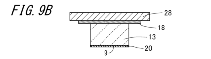
- FIG. 9A shows the bottom surface of the flat-bottomed pool 21 covered with non-woven paper impregnated with the air removal liquid 20, just before the open cut side 9 of the precursor body 13 is brought into contact therewith.
- FIG. 9B shows the blank precursor 13 with the air removal liquid 20 attached to the cutting side 9 .
- the air removal liquid 20 has good wettability with respect to the element precursor 13 and the side green sheets 17, and in addition, it does not dry quickly and dissolves both materials of the element precursor 13 and the side green sheets 17. It is desirable to be a liquid that does not The air removal liquid 20 is applied to the cut side surface 9, contacts the side green sheet 17, and then penetrates into the element precursor 13 or the side green sheet 17 while being pressed by the side green sheet 17. Instead, it remains liquid.
- solvents are not preferred from the above point of view. The solvent dissolves the side green sheets 17 and has good wettability.
- the Ni particles present on the surface move, which may lead to a short circuit between the adjacent exposed internal electrode layers. .
- side green sheets 17 are prepared as shown in FIG. 9C.
- the side green sheet 17 may be a stack of a plurality of green sheets, or a stack of green sheets having different compositions.
- the air removal liquid 20 on the cut side surface 9 of the element precursor 13 is brought into contact with the side green sheet 17, and the element precursor 13 is pressed onto the side green sheet 17 using a pressing machine. impose.
- the air removal liquid 20 sandwiched between the cut side surface 9 and the side green sheet 17 is pushed out of the cut side surface 9 and discharged to the margin of the side green sheet 17 .
- the pressing force may range from 30 Kg/cm 2 to 100 Kg/cm 2 .
- the air removing liquid 20 is pushed out of the cut side surface 9 in the subsequent pressing step, the air contained in the air removing liquid 20 is also discharged together.
- the wettability of the air removing liquid 20 to the cut side surface 9 should be such that the contact angle is close to zero and the liquid spreads over the solid surface to exhibit extended wetting.
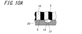
- FIG. 10A schematically shows how the air 31 exists in the recessed portion 19 of the cut side surface 9 after the application of the air removal liquid 20 .
- the surface of the cut side surface 9 where the air 31 exists is not wet at first, but the entire surface of the cut side surface 9 is wetted by the air removal liquid 20 that gradually diffuses, and as shown in FIG. It will exist in 20.
- a plasticizer is used as the air removing liquid 20 in this embodiment.
- the plasticizer enhances the plasticity of the binder of the precursor body 13 or the binder of the side green sheets 17 , and has good wettability to the precursor body 13 by diffusion wettability. Therefore, the surface of the element precursor 13 can be completely wetted without dissolving the element precursor 13 .
- the plasticizer even if the plasticizer is applied while leaving the air 31 in the recess 19 of the cut side surface 9, the plasticizer will penetrate the cut side surface 9 where the air 31 exists so as to wet the cut side surface 9.
- the air 31 is separated from the cut side 9 as shown in 10B, and when the plasticizer is dislodged from the cut side 9 by subsequent pressing, the air 31 moves along with the cut side 9, as shown in FIG. 10C. removed by being pushed away from
- the plasticizer contacts the binder on the surface of the element precursor 13 or the side green sheet 17, the plasticity of the binder on the surface contacted by the plasticizer is enhanced. Similarly, the plasticity of the binder present on the surface to which the side green sheets 17 are attached is also enhanced. As a result, pressure bonding can be effectively performed.
- the binder used for the green sheet of this example is a polyvinyl butyral resin binder
- dioctyl phthalate (DOP) bis(2-ethylhexyl) phthalate (DEHP) or dibutyl phthalate having good compatibility
- Phthalates such as (DBP), phosphates, and fatty acid esters may also be used.
- the base plate on which the side green sheets 17 are placed is desirably a flat hard plate in order to reliably discharge the air removal liquid 20 .
- a flexible sheet may be sandwiched between the press mechanisms.
- an elastic member such as a thin silicon rubber plate may be interposed between the support sheet 18 of the element precursor 13 and the press punch (not shown) instead of the side green sheet 17 side.
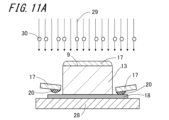
- FIG. 11A is a diagram schematically showing how the blank portion of the side green sheet is cut by dry ice particles.
- the marginal portion (portion other than the portion pressed by the cut side surface 9) of the side green sheet 17 is removed by cutting.
- a portion of the side green sheet 17 other than the portion pressed by the cut side surface 9 is removed with a jet stream containing dry ice particles 30. - ⁇ Since the dry ice particles 30 take heat from the side green sheets 17 and vaporize at the time of collision, the temperature of the side green sheets 17 is lowered and the flexibility is reduced.
- the impact force of the jet stream and the dry ice is applied to the side green sheets 17, so that the margins of the side green sheets 17 that are not supported below bend and the edges of the cut side surfaces 9 of the precursor body 13 are bent. It is cut so that it is torn off at the part. Inside the edge portion, the side green sheet 17 is pressed against the cut side surface 9 by the dry ice jet. This is because the fine particles 30 collide. At this time, the air removing liquid 20 removed from the cut side surface 9 scatters while adhering to the torn side green sheet 17 .
- FIG. 11B is a diagram schematically showing a supporting member that supports the margins of the side green sheets.
- a support member 51 for supporting a portion other than the portion pressed against the cut side surface 9 is arranged around the aligned precursor bodies 13 .
- the cutting environment of the side green sheets 17 existing in the central portion of the precursor body 13 and the side green sheets 17 existing around the periphery of the body precursor 13 can be made the same. This reduces processing time and maintains uniformity in cut quality.
- a dry ice nozzle we used a nozzle that can eject dry ice particles on top of the high pressure air of the jet stream.
- the air pressure ranged from 0.2 MPa, which is the minimum pressure required for sheet cutting, to 0.5 MPa, which is the maximum pressure for air supply in the factory.
- the distance between the dry ice nozzle and the cut side surface, which is the surface to be processed, was 20 to 80 mm, and was appropriately set according to the size of the base plate 28 . When the distance from the surface to be machined is 80 mm or more, cutting becomes difficult even with the maximum air pressure of 0.5 MPa.
- the jet stream may be attenuated, dry ice is a fine particle, so the particles vaporize before collision, reducing the collision effect.
- Dry ice fine particles having an average particle size of 100 microns or less as determined by high-speed photographic observation were used. This is because the surface of the element body of the laminated ceramic part before firing is soft, and therefore, if the average particle diameter is large, the polishing effect is gradually exhibited, and the surface of the side green sheet is uneven.
- the distance between the workpieces can be narrowed as long as there is a gap through which the air stream can pass, so there is an effect that the number of workpieces on the base plate 28 can be increased.
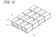
- FIG. 12 shows the state of the raw base component 2 obtained by the above steps, in which side green sheets as protective layers are laid on a pair of cut side surfaces.
- a method for manufacturing a laminated ceramic electronic component cuts a mother laminate in which a plurality of dielectric ceramics and a plurality of internal electrode layers are alternately laminated along a cutting line orthogonal to the mother laminate, Obtaining a plurality of element precursors having cut side surfaces in which the internal electrode layers are exposed, aligning the element precursor so that the cut side surface becomes an open surface; Applying an air removal liquid to the open cut side surface, After the side green sheets are brought into contact with the air removal liquid applied to the cut side surfaces, the side green sheets are pressed.
- a mother laminate in which a plurality of dielectric ceramics and a plurality of internal electrode layers are alternately laminated is cut along a cutting line orthogonal to the mother laminate. obtaining a plurality of element precursors having cut side surfaces in which the internal electrode layers are exposed; aligning the element precursor so that the cut side surface becomes an open surface; Applying an air removal liquid to the open cut side surface, After bringing the side green sheet into contact with the air removal liquid applied to the cut side surface, pressing the side green sheet, A jet stream containing dry ice particles is used to remove the portion of the side green sheet other than the portion pressed by the cut side surface.
- the manufacturing method of the multilayer ceramic electronic component of the present disclosure configured as described above, the voids at the boundary between the cut side surface of the base component and the side margin layer are eliminated, and the insulation degradation or reliability that becomes the product characteristic after firing is eliminated. It is possible to prevent deterioration of
- the blank portion which is the margin for gluing of the side green sheet attached to the side surface of the laminate, can be efficiently cut and removed.
Landscapes
- Engineering & Computer Science (AREA)
- Power Engineering (AREA)
- Manufacturing & Machinery (AREA)
- Microelectronics & Electronic Packaging (AREA)
- Ceramic Engineering (AREA)
- Chemical & Material Sciences (AREA)
- Inorganic Chemistry (AREA)
- Ceramic Capacitors (AREA)
- Fixed Capacitors And Capacitor Manufacturing Machines (AREA)
Abstract
Description
前記内部電極層が露出した切断側面を有する複数の素体前駆体を得て、
前記素体前駆体を前記切断側面が開放面になるように整列させ、
開放されている前記切断側面にエア除去液を付与し、
前記切断側面に付与されたエア除去液に側面グリーンシートを接触させた後、前記側面グリーンシートを押圧する。
前記素体前駆体を前記切断側面が開放面になるように整列させ、
開放されている前記切断側面にエア除去液を付与し、
前記切断側面に付与されたエア除去液に側面グリーンシートを接触させた後、前記側面グリーンシートを押圧し、
ドライアイス微粒子を含んだジェット気流で、前記側面グリーンシートの、前記切断側面に押圧された部分以外の部分を除去する。
2 素体部品
3 外部電極
4 誘電体セラミック
5 内部電極層
6 保護層
7 主面
7a 第1主面
7b 第2主面
8 端面
8a 第1端面
8b 第2端面
9 切断側面
9a 第1側面
9b 第2側面
10 セラミックグリーンシート
11 母積層体
13 素体前駆体
17 側面グリーンシート
18 支持シート
19 凹部
20 エア除去液
21 平底プール
22 振込トレイ
23 ポケット
27 押圧
28 台板
29 ジェット気流
30 ドライアイス微粒子
31 エア
51 支持部材
Claims (6)
- 複数の誘電体セラミックと複数の内部電極層とが交互に積層された母積層体を、該母積層体に直交する切断ラインで切断して、前記内部電極層が露出した切断側面を有する複数の素体前駆体を得て、
前記素体前駆体を前記切断側面が開放面になるように整列させ、
開放されている前記切断側面にエア除去液を付与し、
前記切断側面に付与されたエア除去液に側面グリーンシートを接触させた後、前記側面グリーンシートを押圧する、積層セラミック電子部品の製造方法。 - 前記エア除去液が可塑剤である、請求項1記載の積層セラミック電子部品の製造方法。
- 前記素体前駆体を支持する支持シートとプレスパンチとの間に弾性体を介在させたプレス装置を用いて、前記側面グリーンシートを押圧する、請求項1または2記載の積層セラミック電子部品の製造方法。
- ドライアイス微粒子を含んだジェット気流で、前記側面グリーンシートの、前記切断側面に押圧された部分以外の部分を除去する請求項1~3のいずれか1項記載の積層セラミック電子部品の製造方法。
- 前記側面グリーンシートの、前記切断側面に押圧された部分以外の部分を支持する支持部材を、整列された前記素体前駆体の周辺に配置する、請求項4記載の積層セラミック電子部品の製造方法。
- 複数の誘電体セラミックと複数の内部電極層とが交互に積層された母積層体を、該母積層体に直交する切断ラインで切断して、前記内部電極層が露出した切断側面を有する複数の素体前駆体を得て、
前記素体前駆体を前記切断側面が開放面になるように整列させ、
開放されている前記切断側面にエア除去液を付与し、
前記切断側面に付与されたエア除去液に側面グリーンシートを接触させた後、前記側面グリーンシートを押圧し、
ドライアイス微粒子を含んだジェット気流で、前記側面グリーンシートの、前記切断側面に押圧された部分以外の部分を除去する、積層セラミック電子部品の製造方法。
Priority Applications (2)
| Application Number | Priority Date | Filing Date | Title |
|---|---|---|---|
| JP2023543782A JPWO2023026807A1 (ja) | 2021-08-24 | 2022-08-03 | |
| CN202280057188.6A CN117916831A (zh) | 2021-08-24 | 2022-08-03 | 层叠陶瓷电子部件的制造方法 |
Applications Claiming Priority (2)
| Application Number | Priority Date | Filing Date | Title |
|---|---|---|---|
| JP2021136643 | 2021-08-24 | ||
| JP2021-136643 | 2021-08-24 |
Publications (1)
| Publication Number | Publication Date |
|---|---|
| WO2023026807A1 true WO2023026807A1 (ja) | 2023-03-02 |
Family
ID=85323142
Family Applications (1)
| Application Number | Title | Priority Date | Filing Date |
|---|---|---|---|
| PCT/JP2022/029808 WO2023026807A1 (ja) | 2021-08-24 | 2022-08-03 | 積層セラミック電子部品の製造方法 |
Country Status (3)
| Country | Link |
|---|---|
| JP (1) | JPWO2023026807A1 (ja) |
| CN (1) | CN117916831A (ja) |
| WO (1) | WO2023026807A1 (ja) |
Citations (6)
| Publication number | Priority date | Publication date | Assignee | Title |
|---|---|---|---|---|
| JPS5580310A (en) * | 1978-12-13 | 1980-06-17 | Matsushita Electric Ind Co Ltd | Method of fabricating laminated ceramic capacitor |
| JPH01212419A (ja) * | 1988-02-19 | 1989-08-25 | Murata Mfg Co Ltd | セラミック積層体の製造方法 |
| JPH11111560A (ja) * | 1997-10-06 | 1999-04-23 | Matsushita Electric Ind Co Ltd | セラミック電子部品の製造方法 |
| JP2000299222A (ja) * | 1999-04-15 | 2000-10-24 | Matsushita Electric Ind Co Ltd | 積層セラミック電子部品およびその製造方法 |
| JP2017120880A (ja) * | 2015-12-25 | 2017-07-06 | 太陽誘電株式会社 | 積層セラミック電子部品及びその製造方法 |
| JP2020188192A (ja) * | 2019-05-16 | 2020-11-19 | 株式会社村田製作所 | 電子部品の製造方法 |
-
2022
- 2022-08-03 WO PCT/JP2022/029808 patent/WO2023026807A1/ja active Application Filing
- 2022-08-03 CN CN202280057188.6A patent/CN117916831A/zh active Pending
- 2022-08-03 JP JP2023543782A patent/JPWO2023026807A1/ja active Pending
Patent Citations (6)
| Publication number | Priority date | Publication date | Assignee | Title |
|---|---|---|---|---|
| JPS5580310A (en) * | 1978-12-13 | 1980-06-17 | Matsushita Electric Ind Co Ltd | Method of fabricating laminated ceramic capacitor |
| JPH01212419A (ja) * | 1988-02-19 | 1989-08-25 | Murata Mfg Co Ltd | セラミック積層体の製造方法 |
| JPH11111560A (ja) * | 1997-10-06 | 1999-04-23 | Matsushita Electric Ind Co Ltd | セラミック電子部品の製造方法 |
| JP2000299222A (ja) * | 1999-04-15 | 2000-10-24 | Matsushita Electric Ind Co Ltd | 積層セラミック電子部品およびその製造方法 |
| JP2017120880A (ja) * | 2015-12-25 | 2017-07-06 | 太陽誘電株式会社 | 積層セラミック電子部品及びその製造方法 |
| JP2020188192A (ja) * | 2019-05-16 | 2020-11-19 | 株式会社村田製作所 | 電子部品の製造方法 |
Also Published As
| Publication number | Publication date |
|---|---|
| CN117916831A (zh) | 2024-04-19 |
| JPWO2023026807A1 (ja) | 2023-03-02 |
Similar Documents
| Publication | Publication Date | Title |
|---|---|---|
| JP6131756B2 (ja) | コンデンサ素子の製造方法 | |
| JP2017147358A (ja) | 電子部品の製造方法 | |
| WO2017061324A1 (ja) | 多層セラミック基板の製造方法 | |
| JP4084385B2 (ja) | 積層電子部品用の積層体ユニットの製造方法 | |
| JP7127720B2 (ja) | 積層セラミック電子部品の製造方法 | |
| JPWO2004088686A1 (ja) | 積層セラミック電子部品の製造方法 | |
| WO2023026807A1 (ja) | 積層セラミック電子部品の製造方法 | |
| JPWO2004088685A1 (ja) | 積層セラミック電子部品の製造方法 | |
| JP3527667B2 (ja) | セラミック電子部品の製造方法 | |
| US20240351325A1 (en) | Method for manufacturing multilayer ceramic electronic components | |
| JP2017112320A (ja) | 電子部品の製造方法 | |
| JP2005191409A (ja) | 積層セラミックコンデンサの製造方法 | |
| JP4789443B2 (ja) | 複合シートの製造方法、積層体の製造方法および積層部品の製造方法 | |
| TWI840898B (zh) | 積層陶瓷電子零件及其製造方法 | |
| JP2005259964A (ja) | セラミック積層体の製造方法 | |
| JP4134729B2 (ja) | 積層セラミック電子部品の製造方法 | |
| JP2004186343A (ja) | セラミック積層体及びその製法 | |
| JP4610274B2 (ja) | 電子部品の製造方法 | |
| JP7232010B2 (ja) | 積層セラミック電子部品の製造方法 | |
| JP2004186344A (ja) | セラミック積層体及びその製法 | |
| JP4142686B2 (ja) | 積層電子部品用の積層体ユニットの製造方法 | |
| JP3921454B2 (ja) | 積層セラミック電子部品用の積層体ユニットの製造方法および積層セラミック電子部品用の積層体ユニット | |
| JP2004186341A (ja) | セラミック積層体の製法 | |
| TW202405837A (zh) | 積層陶瓷電子零件 | |
| JP2005056977A (ja) | 積層セラミック基板の製造方法および誘電体積層デバイス |
Legal Events
| Date | Code | Title | Description |
|---|---|---|---|
| 121 | Ep: the epo has been informed by wipo that ep was designated in this application |
Ref document number: 22861098 Country of ref document: EP Kind code of ref document: A1 |
|
| WWE | Wipo information: entry into national phase |
Ref document number: 18683597 Country of ref document: US Ref document number: 2023543782 Country of ref document: JP |
|
| WWE | Wipo information: entry into national phase |
Ref document number: 202280057188.6 Country of ref document: CN |
|
| NENP | Non-entry into the national phase |
Ref country code: DE |
|
| 122 | Ep: pct application non-entry in european phase |
Ref document number: 22861098 Country of ref document: EP Kind code of ref document: A1 |