WO2022265058A1 - 磁性積層膜及び磁気抵抗効果素子 - Google Patents
磁性積層膜及び磁気抵抗効果素子 Download PDFInfo
- Publication number
- WO2022265058A1 WO2022265058A1 PCT/JP2022/024040 JP2022024040W WO2022265058A1 WO 2022265058 A1 WO2022265058 A1 WO 2022265058A1 JP 2022024040 W JP2022024040 W JP 2022024040W WO 2022265058 A1 WO2022265058 A1 WO 2022265058A1
- Authority
- WO
- WIPO (PCT)
- Prior art keywords
- layer
- magnetic
- ferromagnetic
- nonmagnetic
- laminated film
- Prior art date
- Legal status (The legal status is an assumption and is not a legal conclusion. Google has not performed a legal analysis and makes no representation as to the accuracy of the status listed.)
- Ceased
Links
Images
























Classifications
-
- H—ELECTRICITY
- H10—SEMICONDUCTOR DEVICES; ELECTRIC SOLID-STATE DEVICES NOT OTHERWISE PROVIDED FOR
- H10N—ELECTRIC SOLID-STATE DEVICES NOT OTHERWISE PROVIDED FOR
- H10N50/00—Galvanomagnetic devices
- H10N50/10—Magnetoresistive devices
-
- G—PHYSICS
- G11—INFORMATION STORAGE
- G11C—STATIC STORES
- G11C11/00—Digital stores characterised by the use of particular electric or magnetic storage elements; Storage elements therefor
- G11C11/02—Digital stores characterised by the use of particular electric or magnetic storage elements; Storage elements therefor using magnetic elements
- G11C11/16—Digital stores characterised by the use of particular electric or magnetic storage elements; Storage elements therefor using magnetic elements using elements in which the storage effect is based on magnetic spin effect
- G11C11/161—Digital stores characterised by the use of particular electric or magnetic storage elements; Storage elements therefor using magnetic elements using elements in which the storage effect is based on magnetic spin effect details concerning the memory cell structure, e.g. the layers of the ferromagnetic memory cell
-
- G—PHYSICS
- G11—INFORMATION STORAGE
- G11C—STATIC STORES
- G11C11/00—Digital stores characterised by the use of particular electric or magnetic storage elements; Storage elements therefor
- G11C11/02—Digital stores characterised by the use of particular electric or magnetic storage elements; Storage elements therefor using magnetic elements
- G11C11/16—Digital stores characterised by the use of particular electric or magnetic storage elements; Storage elements therefor using magnetic elements using elements in which the storage effect is based on magnetic spin effect
- G11C11/165—Auxiliary circuits
- G11C11/1673—Reading or sensing circuits or methods
-
- G—PHYSICS
- G11—INFORMATION STORAGE
- G11C—STATIC STORES
- G11C11/00—Digital stores characterised by the use of particular electric or magnetic storage elements; Storage elements therefor
- G11C11/02—Digital stores characterised by the use of particular electric or magnetic storage elements; Storage elements therefor using magnetic elements
- G11C11/16—Digital stores characterised by the use of particular electric or magnetic storage elements; Storage elements therefor using magnetic elements using elements in which the storage effect is based on magnetic spin effect
- G11C11/165—Auxiliary circuits
- G11C11/1675—Writing or programming circuits or methods
-
- H—ELECTRICITY
- H10—SEMICONDUCTOR DEVICES; ELECTRIC SOLID-STATE DEVICES NOT OTHERWISE PROVIDED FOR
- H10B—ELECTRONIC MEMORY DEVICES
- H10B61/00—Magnetic memory devices, e.g. magnetoresistive RAM [MRAM] devices
-
- H—ELECTRICITY
- H10—SEMICONDUCTOR DEVICES; ELECTRIC SOLID-STATE DEVICES NOT OTHERWISE PROVIDED FOR
- H10B—ELECTRONIC MEMORY DEVICES
- H10B61/00—Magnetic memory devices, e.g. magnetoresistive RAM [MRAM] devices
- H10B61/20—Magnetic memory devices, e.g. magnetoresistive RAM [MRAM] devices comprising components having three or more electrodes, e.g. transistors
-
- H—ELECTRICITY
- H10—SEMICONDUCTOR DEVICES; ELECTRIC SOLID-STATE DEVICES NOT OTHERWISE PROVIDED FOR
- H10B—ELECTRONIC MEMORY DEVICES
- H10B61/00—Magnetic memory devices, e.g. magnetoresistive RAM [MRAM] devices
- H10B61/20—Magnetic memory devices, e.g. magnetoresistive RAM [MRAM] devices comprising components having three or more electrodes, e.g. transistors
- H10B61/22—Magnetic memory devices, e.g. magnetoresistive RAM [MRAM] devices comprising components having three or more electrodes, e.g. transistors of the field-effect transistor [FET] type
-
- H—ELECTRICITY
- H10—SEMICONDUCTOR DEVICES; ELECTRIC SOLID-STATE DEVICES NOT OTHERWISE PROVIDED FOR
- H10D—INORGANIC ELECTRIC SEMICONDUCTOR DEVICES
- H10D48/00—Individual devices not covered by groups H10D1/00 - H10D44/00
- H10D48/40—Devices controlled by magnetic fields
-
- H—ELECTRICITY
- H10—SEMICONDUCTOR DEVICES; ELECTRIC SOLID-STATE DEVICES NOT OTHERWISE PROVIDED FOR
- H10N—ELECTRIC SOLID-STATE DEVICES NOT OTHERWISE PROVIDED FOR
- H10N50/00—Galvanomagnetic devices
- H10N50/80—Constructional details
-
- H—ELECTRICITY
- H10—SEMICONDUCTOR DEVICES; ELECTRIC SOLID-STATE DEVICES NOT OTHERWISE PROVIDED FOR
- H10N—ELECTRIC SOLID-STATE DEVICES NOT OTHERWISE PROVIDED FOR
- H10N50/00—Galvanomagnetic devices
- H10N50/80—Constructional details
- H10N50/85—Materials of the active region
-
- H—ELECTRICITY
- H10—SEMICONDUCTOR DEVICES; ELECTRIC SOLID-STATE DEVICES NOT OTHERWISE PROVIDED FOR
- H10N—ELECTRIC SOLID-STATE DEVICES NOT OTHERWISE PROVIDED FOR
- H10N52/00—Hall-effect devices
- H10N52/80—Constructional details
- H10N52/85—Materials of the active region
Definitions
- the present invention relates to a magnetic laminated film and a magnetoresistance effect element.
- spin injection magnetization switching which consists of a recording layer having magnetization that can be switched, a barrier layer made of an insulator, and a magnetization layer.
- the magnetization of the recording layer is reversed by passing a current through a magnetic tunnel junction (MTJ) consisting of a reference layer whose direction is fixed.
- MTJ magnetic tunnel junction
- SOT spin orbit torque
- MRAM Magnetic Random Access Memory
- the SOT-MRAM element is configured by providing an MTJ including a recording layer/barrier layer/reference layer in a heavy metal layer.
- the direction of magnetization in the recording layer switches between parallel and antiparallel to the direction of magnetization in the reference layer, and the data are recorded (Patent Documents 1 to 3).
- Non-Patent Document 1 The ferromagnetic moment of NiFe is reversed by an external magnetic field, which induces rotation of the antiferromagnetic moment of IrMn exchange-coupled with NiFe. Tunneling anisotropic magnetoresistance (TAMR) has been detected with the rotation of the IrMn moment.
- TAMR Tunneling anisotropic magnetoresistance
- one object of the present invention is to provide a magnetic laminated film that allows a write current to flow and realizes high density and/or high speed memory, and a magnetoresistive effect element using the same.
- the concept of the present invention is as follows. [1] a first ferromagnetic layer; an antiferromagnetic coupling layer provided on the first ferromagnetic layer; a second ferromagnetic layer provided on the antiferromagnetic coupling layer; including A magnetic multilayer film, wherein the antiferromagnetic coupling layer includes a first nonmagnetic layer and an interlayer coupling nonmagnetic layer. [2] The antiferromagnetic coupling layer is provided on the first nonmagnetic layer, the interlayer coupling nonmagnetic layer provided on the first nonmagnetic layer, and the interlayer coupling nonmagnetic layer. and a second non-magnetic layer.
- a third nonmagnetic layer is provided on the surface of the first ferromagnetic layer opposite to the antiferromagnetic coupling layer and/or the surface of the second ferromagnetic layer opposite to the antiferromagnetic coupling layer.
- the magnetic multilayer film according to any one of [1] to [6]; a recording layer including a ferromagnetic layer or an antiferromagnetic layer provided on the magnetic laminated film; a barrier layer made of an insulator and provided on the recording layer; a reference layer provided on the barrier layer; and the first ferromagnetic layer or the second ferromagnetic layer of the magnetic laminated film and the ferromagnetic layer or the antiferromagnetic layer of the recording layer are coupled by exchange interaction, Magnetoresistance in which the magnetization of the first ferromagnetic layer and the second ferromagnetic layer is reversed by passing a current in a direction intersecting the stacking direction of the magnetic multilayer film, and the magnetization of the recording layer is reversed.
- the magnetic laminated film is configured by providing a third non-magnetic layer on the recording layer side of the magnetic laminated film or on the side opposite to the recording layer, wherein the third nonmagnetic layer is made of a metal or alloy containing at least one of W, Cu, Ta, and Mn; The magnetoresistive element according to any one of [7] to [9].
- a third nonmagnetic layer is provided on the recording layer side of the magnetic laminated film, and a fourth nonmagnetic layer is provided on the opposite side of the magnetic laminated film to the recording layer.
- the third nonmagnetic layer and the fourth nonmagnetic layer are made of a metal or alloy containing at least one of W, Cu, Ta, and Mn;
- the magnetoresistive element according to any one of [7] to [9].
- the ferromagnetic layer in contact with the third nonmagnetic layer has magnetization inclined in the direction of current application of the conductive layer.
- a first ferromagnetic layer an antiferromagnetic coupling layer provided on the first ferromagnetic layer; a second ferromagnetic layer provided on the antiferromagnetic coupling layer; including The first ferromagnetic layer and the second ferromagnetic layer are antiferromagnetically coupled, the antiferromagnetic coupling layer comprises a first nonmagnetic layer and an interlayer coupling nonmagnetic layer, the first non-magnetic layer is made of a metal or alloy containing Pt, A magnetic laminated film, wherein the interlayer coupling non-magnetic layer is made of a metal or alloy containing at least one of Ir, Rh and Ru.
- a first ferromagnetic layer comprising a first nonmagnetic layer, the interlayer coupling nonmagnetic layer provided on the first nonmagnetic layer, and a second interlayer coupling nonmagnetic layer provided on the interlayer coupling nonmagnetic layer.
- a third nonmagnetic layer is provided on the surface of the first ferromagnetic layer opposite to the antiferromagnetic coupling layer and/or the surface of the second ferromagnetic layer opposite to the antiferromagnetic coupling layer.
- the present invention it is possible to provide a magnetic laminated film that allows a write current to flow and realizes high density and/or high speed memory, and a magnetoresistive effect element using the same.
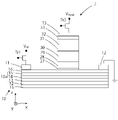
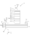
- FIG. 1A is a plan view of a magnetic laminated film and a magnetoresistive effect element using the same according to the first embodiment of the present invention.
- FIG. 1B is a cross-sectional view along line AA in FIG. 1A.
- FIG. 2A is a diagram for explaining a state in which data "0" is written to the recording layer by applying a current to the magnetic laminated film according to the first embodiment of the present invention.
- FIG. 2B is a diagram for explaining a state in which data "1" is written in the recording layer by flowing a current in the opposite direction through the magnetic laminated film according to the first embodiment of the present invention.
- FIG. 1A is a plan view of a magnetic laminated film and a magnetoresistive effect element using the same according to the first embodiment of the present invention.
- FIG. 1B is a cross-sectional view along line AA in FIG. 1A.
- FIG. 2A is a diagram for explaining a state in which data "0" is written to the recording layer by
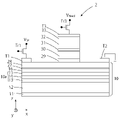
- FIG. 3A is a plan view of a magnetic laminated film and a magnetoresistive effect element using the same according to a second embodiment of the present invention.
- FIG. 3B is a cross-sectional view along line BB in FIG. 3A.
- FIG. 3C is a cross-sectional view of the magnetic laminated film and the magnetoresistance effect element according to the second embodiment of the present invention from another viewpoint.
- FIG. 3D is another cross-sectional view of the magnetic laminated film and the magnetoresistive element according to the second embodiment of the present invention.
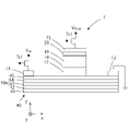
- FIG. 4A is a plan view of a magnetic laminated film and a magnetoresistive effect element using the same according to a third embodiment of the present invention.
- FIG. 4B is a cross-sectional view along line CC in FIG.
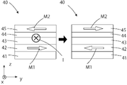
- FIG. 5A is a diagram for explaining a state in which data "0" is written to the recording layer by applying a current to the magnetic laminated film according to the third embodiment of the present invention.
- FIG. 5B is a diagram for explaining a state in which data "1" is written in the recording layer by flowing a current in the opposite direction through the magnetic laminated film according to the third embodiment of the present invention.
- FIG. 6A is a plan view of a magnetic laminated film and a magnetoresistive effect element using the same according to a fourth embodiment of the present invention.
- FIG. 6B is a cross-sectional view along line DD in FIG. 6A.
- FIG. 6C is a cross-sectional view from another viewpoint of the magnetic laminated film and the magnetoresistance effect element according to the fourth embodiment of the present invention.
- FIG. 6D is another cross-sectional view of the magnetic laminated film and the magnetoresistive element according to the fourth embodiment of the present invention.
- 7 is a magnetization curve of the sample of Demonstration Example 1.
- FIG. 8 is a magnetization curve of the sample of Demonstration Example 2.
- FIG. 9 is a magnetization curve of the sample of Demonstration Example 3.
- FIG. 10 is a graph showing the dependence of the interlayer coupling force J ex (mJ/m 2 ) on the total thickness t total (nm) of the non-magnetic layers.
- FIG. 11 is a magnetization curve of the sample of Demonstration Example 5.
- FIG. 12 is a magnetization curve of the sample of Demonstration Example 6.
- FIG. 13 is a magnetization curve of the sample of Demonstration Example 7.
- FIG. 14 is a magnetization curve of the sample of Demonstration Example 8.
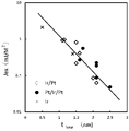
- FIG. 15 is a graph showing the dependence of the interlayer coupling force J ex (mJ/m 2 ) on the total thickness t total (nm) of the non-magnetic layers.
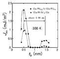
- FIG. 16 shows the Ir thickness dependence of the interlayer bond strength J ex .
- FIG. 17 shows Ru thickness dependence of the interlayer bond strength J ex .
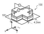
- FIG. 18 is a diagram schematically showing a Hall bar and a measurement system produced as sample 29.
- FIG. 19A is a cross-sectional view of the fabricated sample 29.
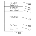
- FIG. 19B is a cross-sectional view of a manufactured sample of Comparative Example 2.
- FIG. 20 is a diagram showing the pulse current dependence of the Hall resistance Rxy ( ⁇ ) of Sample 29 and Comparative Example 2.
- FIG. 21A is a diagram showing the dependence of the spin generation efficiency on the Ir layer thickness for samples 30 to 34.
- FIG. 21B is a diagram showing the interlayer coupling force Jex (mJ/m 2 ) dependence of the spin generation efficiency for Samples 30 to 34.
- FIG. FIG. 22A is a diagram showing the dependence of the spin generation efficiency on the Pt layer thickness for samples 35 to 39.
- FIG. 22B is a diagram showing the interlayer coupling force Jex (mJ/m 2 ) dependence of the spin generation efficiency for samples 35 to 39.
- FIG. FIG. 23A is a plan view of a magnetoresistive element according to the fifth embodiment.
- FIG. 23B is a cross-sectional view along line EE in FIG. 23A.
- FIG. 24 is a cross-sectional view of a magnetoresistive element according to the sixth embodiment.
- FIG. 25 is a cross-sectional view of a magnetoresistive element according to the seventh embodiment.
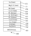
- 26 is a cross-sectional view of Demonstration Example 10.
- FIG. FIG. 27 is an electron microscope image of the Hall bar produced in Demonstration Example 10.
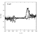
- 28B shows the dependence of the Hall resistance Rxy ( ⁇ ) on the pulse current in Demonstration Example 10.
- the pulse current I was 200 ⁇ s
- the constant external magnetic field Hex was 28.5 mT and 18 mT
- the pulse current I was 28.5 mT and 18 mT.
- FIG. 28C shows the dependence of the Hall resistance Rxy ( ⁇ ) on the pulse current in Demonstration Example 10.
- the pulse current I was 200 ⁇ s
- the constant external magnetic field Hex was 8 mT and 0 mT
- FIG. 28D shows the dependence of the Hall resistance Rxy ( ⁇ ) on the pulse current in Demonstration Example 10.
- the pulse current I was 200 ⁇ s
- the constant external magnetic field Hex was ⁇ 6.5 mT, ⁇ 16.5 mT
- FIG. 28E shows the dependence of the Hall resistance Rxy ( ⁇ ) on the pulse current in Demonstration Example 10.
- the pulse current I was 200 ⁇ s
- the constant external magnetic field Hex was ⁇ 27 mT, ⁇ 37 mT
- the pulse current I was
- FIG. 28F shows the dependence of the Hall resistance Rxy ( ⁇ ) on the pulse current in Demonstration Example 10.
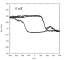
- FIG. FIG. 30 is a diagram showing the results of the pulse current dependence of the Hall resistance Rxy ( ⁇ ) in Demonstration Example 11 when the pulse current I was applied for 200 ⁇ s and a constant external magnetic field Hex was not applied during measurement. be.
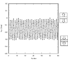
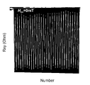
- FIG. 31 is a diagram showing the dependence of the Hall resistance Rxy(Ohm) on the number of repetitions when pulse currents are alternately applied in ⁇ directions in no magnetic field in Demonstration Example 11.
- FIG. 32 is a cross-sectional view of Demonstration Example 12.
- FIG. 33 is a diagram showing the pulse current dependence of the Hall resistance Rxy( ⁇ ) in Demonstration Example 12.
- FIG. 34 is a diagram showing pulse current dependence of Hall resistance Rxy( ⁇ ) in Demonstration Example 13.
- FIG. 35 is a diagram showing pulse current dependence of the Hall resistance Rxy ( ⁇ ) in Demonstration Example 14.
- FIG. FIG. 36 is a diagram showing pulse current dependence of Hall resistance Rxy ( ⁇ ) in Demonstration Example 15.
- FIG. FIG. 37 is a diagram showing pulse current dependence of the Hall resistance Rxy( ⁇ ) in Demonstration Example 16.
- FIG. 38 is a diagram showing the dependence of the Hall resistance Rxy(Ohm) on the number of repetitions when pulse currents are alternately applied in ⁇ directions in no magnetic field in Demonstration Example 16.
- FIG. 39 is a graph showing pulse current dependence of Hall resistance Rxy ( ⁇ ) in Comparative Example 3.
- FIG. 40 is a cross-sectional view of Comparative Example 4.
- FIG. FIG. 41A shows the dependence of the Hall resistance Rxy( ⁇ ) on the pulse current in Comparative Example 4.
- FIG. 41B shows the pulse current dependence of the Hall resistance Rxy( ⁇ ) in Comparative Example 4 when the pulse current I was applied for 200 ⁇ s and the constant external magnetic field Hex was not applied during the measurement.
- FIG. 4 is a diagram showing;
- FIG. 41C shows the dependence of the Hall resistance Rxy( ⁇ ) on the pulse current in Comparative Example 4.
- FIG. 1A is a plan view of a magnetic laminated film and a magnetoresistive effect element using the same according to a first embodiment of the present invention
- FIG. 1B is a cross-sectional view along line AA.
- the magnetic laminated film 10 according to the first embodiment of the present invention includes an underlayer 11 provided on a substrate (not shown) and a second layer provided on the underlayer 11 .
- the magnetic laminated film 10 is configured as follows.
- a first nonmagnetic layer 13 and a second nonmagnetic layer 15 are in contact with the corresponding upper and lower surfaces of the interlayer coupling layer 14 to sandwich the interlayer coupling layer 14.
- the magnetic layer 16 is in contact with the lower surface of the first nonmagnetic layer 13 and the upper surface of the second nonmagnetic layer 15 to form the first nonmagnetic layer 13 , the interlayer coupling layer 14 , and the second nonmagnetic layer 15 .
- the first ferromagnetic layer 12 is provided in contact with the lower surface of the first nonmagnetic layer 13, and the second ferromagnetic layer 16 is provided in contact with the upper surface of the second nonmagnetic layer 15.
- a recording layer 17 made of a material capable of reversing magnetization is formed on the second ferromagnetic layer 16 .
- the first nonmagnetic layer 13, the interlayer coupling layer 14, and the second nonmagnetic layer 15 constitute the antiferromagnetic coupling layer 10a.
- the interlayer coupling layer 14 may also be called an interlayer coupling non-magnetic layer.
- the antiferromagnetic coupling layer 10a is provided on the first nonmagnetic layer 13, the interlayer coupling nonmagnetic layer (interlayer coupling layer 14) provided on the first nonmagnetic layer 13, and the interlayer coupling nonmagnetic layer. and a second non-magnetic layer 15 .
- FIG. 2A is a diagram for explaining a state in which data "0" is written to the recording layer 17 by applying a current to the magnetic laminated film 10 according to the first embodiment of the present invention.
- the magnetization directions of the first ferromagnetic layer 12 and the second ferromagnetic layer 16 are opposite to each other before the current is passed in the -x direction.
- a spin current flow of spin motion
- the spin Hall effect due to the spin interaction
- the spins in the opposite directions are induced in the magnetic laminated films 10 ⁇ z.
- the interlayer coupling layer 14 is sandwiched between the first non-magnetic layer 13 and the second non-magnetic layer 15 of the magnetic laminated film 10.
- the spin torque is increased in comparison, and the magnetizations of the first ferromagnetic layer 12 and the second ferromagnetic layer 16 can be reversed.
- the magnetic laminated film 10 shown in FIG. 2A has two ferromagnetic layers and is antiferromagnetically coupled, so that the thermal stability constant ⁇ can be increased. can.
- the conventional SOT element does not have the first ferromagnetic layer 12 at the bottom, only the spin current accumulated at the interface between the second ferromagnetic layer 16 and the second non-magnetic layer 15 is used for magnetization reversal.
- the first ferromagnetic layer 16 and the second nonmagnetic layer 15 generated when a current pulse is applied, but also the first Since both of the spin currents accumulated at the interface between the ferromagnetic layer 12 and the first nonmagnetic layer 13 can be utilized, the energy efficiency of reversal can be doubled.
- the magnetic laminated film 10 is not provided with the first nonmagnetic layer 13 and the second nonmagnetic layer 15, and the interlayer coupling layer 14 is formed between the first ferromagnetic layer 12 and the second ferromagnetic layer.
- the interlayer coupling layer 14 is made of Ru or Ir and achieves antiferromagnetic coupling, the spin Hall angle of Ru and Ir is very small. It is very difficult to achieve magnetization reversal.
- the large spin Hall effect of the first nonmagnetic layer 13 and the second nonmagnetic layer 15 can be used, compared to the case without the first nonmagnetic layer 13 and the second nonmagnetic layer 15, the Spin reversal current can be significantly reduced.
- FIG. 2B is a diagram for explaining a state in which data "1" is written in the recording layer 17 by flowing a current in the opposite direction to the magnetic laminated film 10 according to the first embodiment of the present invention.
- the magnetization directions of the first ferromagnetic layer 12 and the second ferromagnetic layer 16 are opposite to each other before the current is passed in the opposite +x direction.
- a spin current flow of spin motion
- the spins in opposite directions flow in the ⁇ z directions of the respective magnetic laminated films 10.
- the spin current flowing through the magnetic laminated film 10 causes the spins directed in one direction and the spins directed in the other direction to move up and down, respectively. , and flow toward the first ferromagnetic layer 12 and the second ferromagnetic layer 16, respectively. Therefore, as shown in FIG. 2B, the magnetizations M1 and M2 of the first ferromagnetic layer 12 and the second ferromagnetic layer 16 are opposite to those before the current is applied in the +x direction. In this way, by passing a current through the magnetic laminated film 10 in the +x direction, a spin-orbit torque is generated by the current, and the magnetization of each of the first ferromagnetic layer 12 and the second ferromagnetic layer 16 is reversed.
- the antiferromagnetic coupling is maintained in the magnetic laminated film of the first ferromagnetic layer/interlayer coupling layer/second ferromagnetic layer
- the antiferromagnetic coupling is maintained even when the interlayer coupling layer 14 is sandwiched between the first nonmagnetic layer 13 and the second nonmagnetic layer 15 to form the magnetic laminated film 10 .
- This will be explained in a demonstration example to be described later.
- FIGS. 2A and 2B illustrate the case of in-plane magnetization, the same applies to the case of perpendicular magnetization.
- the magnetic laminated film 10 has a surface on which an antiferromagnetic layer for reading as a recording layer 17 is provided on the second ferromagnetic layer 16, and the recording layer 17 having reversible magnetization is provided.
- An Ir--Mn alloy, Fe--Mn alloy, or the like is preferably used for the readout antiferromagnetic layer.
- a barrier layer (also referred to as a tunnel barrier layer) 18 is provided on the recording layer 17 so as to be in contact therewith.
- the barrier layer 18 is made of an insulating material such as MgO, Al 2 O 3 , AlN or MgAlO, and is preferably epitaxially grown on the Ir--Mn alloy or Fe--Mn alloy.
- a non-magnetic layer 19 is provided on the barrier layer 18 as a reference layer. Although the non-magnetic layer 19 is not particularly limited, it is preferably made of Pt, Al, Cu, or the like.
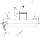
- a lamination of the recording layer 17, the barrier layer 18, and the non-magnetic layer 19 constitutes the magnetoresistive element 1 using the tunneling anisotropic magnetoresistive (TAMR) effect.
- TAMR tunneling anisotropic magnetoresistive
- the reading antiferromagnetic layer as the recording layer 17 and the second ferromagnetic layer 16 are coupled by the exchange coupling action, and the magnetization reversal in the second ferromagnetic layer 16 causes the reading antiferromagnetic layer to Since the antiferromagnetic moment in
- a first terminal T1 and a second terminal T2 are provided on either the uppermost surface or the lowermost surface of the magnetic laminated film 10, and the first terminal T1 and the second terminal T2 are connected to the magnetic laminated film. 10 are separated in a direction orthogonal to the stacking direction.
- a write current flows between the first terminal T1 and the second terminal T2.
- a cap layer 20 is provided on the non-magnetic layer 19 to provide a third terminal T3, and a read current can be passed through the third terminal T3.
- one end of the transistor Tr1 is connected to the first terminal T1, and the second terminal T2 is grounded.
- Vw write voltage
- One end of a transistor Tr3 is connected to the second terminal T2.
- a read voltage V Read a current flows from the third terminal T3 to the second terminal T2.
- the reading antiferromagnetic layer as the recording layer 17 and the second ferromagnetic layer 16 are coupled by the exchange coupling action, and the magnetization reversal in the second ferromagnetic layer 16 causes the reading antiferromagnetic layer to The antiferromagnetic moment at rotates. As the direction of the antiferromagnetic magnetic moment changes, the resistance greatly changes, so that the recording layer 17 can be read.
- the magnitude of the read current differs, so that it is determined whether the data recorded in the readout diamagnetic layer as the recording layer 17 is "0" or "1". can do.
- the interlayer bonding layer 14 is made of a metal or alloy containing at least one of Ir, Rh and Ru.
- Ir is included, it is preferable to have a thickness in the range of 0.4 nm or more and 0.7 nm or less.
- Ru it is preferable to have a thickness in the range of 0.6 nm or more and 0.9 nm or less.
- the interlayer bonding layer 14 is preferably made of a metal or alloy having an fcc structure containing at least one of Ir and Rh.
- interlayer bonding layer 14 be made of a metal or alloy having an fcc structure, including any of Ir, Ir--Os alloy, Rh, Ir--Rh alloy, Ir--Re alloy, and Ir--Ru alloy.
- the first nonmagnetic layer 13 and the second nonmagnetic layer 15 are made of a metal or alloy containing Pt.
- the first nonmagnetic layer 13 and the second nonmagnetic layer 15 are preferably made of a metal or alloy containing Pt and having an fcc structure.
- the first nonmagnetic layer 13 and the second nonmagnetic layer 15 are made of a metal or alloy having an fcc structure such as Pt, Pt--Au alloy, Pt--Ir alloy, Pt--Cu alloy, or Pt--Cr alloy. It is particularly preferred to be selected.
- the first non-magnetic layer 13 and the second non-magnetic layer 15 may be a Pt--Pd alloy, a Pt--Hf alloy, or a Pt--Al alloy.
- the magnetic laminated film 10 even if the interlayer coupling layer 14 is sandwiched between the first nonmagnetic layer 13 and the second nonmagnetic layer 15, the first ferromagnetic Layer 12 and second ferromagnetic layer 16 are antiferromagnetically coupled. Therefore, the magnetic laminated film 10 itself has a structure in which no leakage magnetic field is generated, and has good thermal stability. In order to form a more perfect antiferromagnetic coupling, the first ferromagnetic layer 12 and the second ferromagnetic layer 16 preferably have the same thickness.
- a diamagnetic layer for reading as a recording layer 17 coupled by exchange interaction, and a diamagnetic layer for reading A barrier layer 18 provided on the layer and a fixed layer made of a non-magnetic layer 19 are provided on the second ferromagnetic layer 16. Since the recording layer 17 is coupled with the magnetization of the second ferromagnetic layer 16 by exchange interaction, it has a structure in which no leakage magnetic field is generated. Therefore, the magnetoresistive element 1 itself does not generate a leakage magnetic field. In addition, since the thermal stability is determined by the volume of the magnetic material of the magnetic laminated film 10, as shown in FIG. It can be seen that the volume of the magnetic material is over the entire bottom electrode, and is much better than the read element including T3.
- a magnetic memory such as an MRAM can be obtained. Even if it is integrated as a device, erroneous writing and erroneous reading due to leakage magnetic fields are reduced as much as possible.
- the first ferromagnetic layer 12 and the second ferromagnetic layer 16 may be either in-plane magnetized or perpendicularly magnetized.
- in-plane magnetization as shown in FIG. It may be any of the xy directions inclined to the direction. That is, type Y in which the axis of easy magnetization is parallel/antiparallel to the spin, type X or type Z in which the direction of easy magnetization is orthogonal to the spin may be used.
- FIG. 3A is a plan view of a magnetic laminated film and a magnetoresistive effect element using the same according to a second embodiment of the present invention
- FIG. 3B is a cross-sectional view taken along line BB.
- the magnetic laminated film 10 according to the second embodiment of the present invention has the same configuration as the first embodiment, and therefore has the same effects as the first embodiment. A detailed description is omitted because it overlaps.
- the recording layer 28 including a ferromagnetic layer is provided on the second ferromagnetic layer 16 with the nonmagnetic layer 27 interposed therebetween. It separates the crystal structure from the ferromagnetic layer 16 .
- a ferromagnetic layer as the recording layer 28 is composed of CoFeBo, FeB, CoB, or the like.
- a barrier layer 29 is provided in contact with the reference layer 30 .
- a non-magnetic layer 31 is provided on the side opposite to the reference layer 30 adjacent to the barrier layer 29 to divide the crystal structure of the layers above and below the non-magnetic layer 31 .
- the nonmagnetic layers 27 and 31 are made of one or more elements selected from W, Ta, Mo, Hf, and the like.
- both the ferromagnetic layer and the pinned layer may be called a reference layer.
- the above m and n are arbitrary natural numbers.
- a cap layer 33 is provided on the opposite side of the fixed layer 32 to the non-magnetic layer 31 , and a third terminal T ⁇ b>3 is attached to the cap layer 33 .
- a third terminal T3 is connected to the transistor Tr3.
- a ferromagnetic layer as a recording layer 28 coupled by exchange interaction is provided on the second ferromagnetic layer 16, and a It is configured as a so-called MTJ element having a barrier layer 29 and a reference layer 30 which are separated from each other.
- a first terminal T1 and a second terminal T2 are provided on either the uppermost surface or the lowermost surface of the magnetic laminated film 10, and the first terminal T1 and the second terminal T2 are connected to the magnetic laminated film. 10 are separated in a direction orthogonal to the stacking direction. A write current flows between the first terminal T1 and the second terminal T2.
- data can be written by passing a current between the first terminal T1 and the second terminal T2, as in the first embodiment. Therefore, the description is omitted.
- the magnetization of the recording layer 28 changes from the magnitude of the current flowing through the recording layer 28, the barrier layer 29, and the reference layer 30, which constitute the MTJ element. It can be determined whether the magnetization is parallel or antiparallel to the magnetization of the magnet, and the data can be read.
- the magnetic laminated film 10 even if the interlayer coupling layer 14 is sandwiched between the first nonmagnetic layer 13 and the second nonmagnetic layer 15, the first ferromagnetic Layer 12 and second ferromagnetic layer 16 are antiferromagnetically coupled. Therefore, the magnetic laminated film 10 itself has a structure in which no leakage magnetic field is generated. Since there are two ferromagnetic layers and they are antiferromagnetically coupled, the thermal stability constant ⁇ can be increased.
- the conventional SOT element does not have the first ferromagnetic layer 12 at the bottom, only the spin current accumulated at the interface between the second ferromagnetic layer 16 and the second non-magnetic layer 15 is used for magnetization reversal.
- the spin current accumulated at the interface between the second ferromagnetic layer 16 and the second nonmagnetic layer 15 generated when a current pulse is applied, but also the spin current between the first ferromagnetic layer 12 and the first Since both of the spin currents accumulated at the interface of the non-magnetic layer 13 can be utilized, the energy efficiency of reversal can be doubled.
- the first ferromagnetic layer 12 and the second ferromagnetic layer 16 preferably have the same thickness.
- the write efficiency is further improved.
- the write speed is improved by using the magnetic laminated film 10 in which such antiferromagnetic coupling is maintained.
- FIG. 3C is a cross-sectional view of the magnetic laminated film 10 and the magnetoresistive element 2 according to the second embodiment of the present invention from another viewpoint. As shown in FIG.
- FIG. 3C is another cross-sectional view of the magnetic laminated film 10 and the magnetoresistive element 2 according to the second embodiment of the present invention. As shown in FIG. 3D, the entire Co layer 34/Ir layer 35/Co layer 36/nonmagnetic layer 27/recording layer 28 having an antiferromagnetic coupling structure may be used as the recording layer 28A.
- the Co layers 34 and 36 may be ferromagnetic layers other than Co. Not only the Ir layer 35 but also a Ru layer made of the material of the interlayer bonding layer, for example, may be used.
- the reference layer 30 and the fixed layer 32 can be prevented from generating a leakage magnetic field by adjusting the thickness of the films that constitute them. Therefore, the magnetoresistive element 2 itself does not generate a leakage magnetic field.
- MTJ elements having a ferromagnetic layer as a recording layer 28, a barrier layer 29 provided on the recording layer 28, and a reference layer 30 on at least one magnetic laminated film 10
- a magnetic memory device such as MRAM
- the first ferromagnetic layer 12, the second ferromagnetic layer 16, the recording layer 28, and the reference layer 30 have in-plane magnetization, Any perpendicular magnetization is acceptable.
- the direction of magnetization is not limited to the direction perpendicular to the direction of the current I. It may be in the x-direction, the y-direction, or in the xy-plane. That is, type Y in which the axis of easy magnetization is parallel/antiparallel to the spin, type X or type Z in which the direction of easy magnetization is orthogonal to the spin may be used.
- FIG. 4A is a plan view of a magnetic laminated film and a magnetoresistive effect element using the same according to a third embodiment of the present invention
- FIG. 4B is a cross-sectional view taken along line CC.
- the magnetic laminated film 40 according to the third embodiment of the present invention includes an underlayer 41 provided on a substrate (not shown) and a second layer 41 provided on the underlayer 41 .
- the magnetic laminated film 40 is configured as follows.
- the interlayer coupling layer 43 and the first nonmagnetic layer 44 are in contact with each other.
- the first ferromagnetic layer 42 and the second ferromagnetic layer 45 sandwich the interlayer coupling layer 43 and the first non-magnetic layer 44 in contact with each other at the upper surface, and the first ferromagnetic layer 42 sandwiches the interlayer coupling layer 43 .
- the second ferromagnetic layer 45 is provided in contact with the upper surface of the first nonmagnetic layer 44 .
- the non-magnetic layer is in the form of one layer instead of two layers like the magnetic laminated film 10 according to the first embodiment.
- a recording layer 17 made of a material capable of reversing magnetization is formed on the second ferromagnetic layer 45 .
- the interlayer coupling layer 43 and the first nonmagnetic layer 44 constitute an antiferromagnetic coupling layer 40a.
- the interlayer coupling layer 43 may be called an interlayer coupling non-magnetic layer. Note that the interlayer coupling layer 43 and the first non-magnetic layer 44 may be upside down. The first nonmagnetic layer 44 may simply be called the nonmagnetic layer 44 .
- FIG. 5A is a diagram for explaining a state in which data "0" is written to the recording layer 17 by applying a current to the magnetic laminated film 40 according to the third embodiment of the present invention.
- the magnetization directions of the first ferromagnetic layer 42 and the second ferromagnetic layer 45 are opposite to each other before the current is passed in the -x direction.
- a spin current flow of spin motion
- the spin Hall effect due to the spin interaction
- the spins in the opposite directions are induced in the magnetic laminated films 40 ⁇ z.
- the second ferromagnetic layer 45 is in contact with the first nonmagnetic layer 44 having a large spin Hall angle.
- the spin torque is increased as compared with the case where the layer 44 is not provided, and the magnetizations of the first ferromagnetic layer 42 and the second ferromagnetic layer 45 can be reversed at the same time.
- FIG. 5B is a diagram for explaining a state in which data "1" is written in the recording layer 17 by flowing a current in the opposite direction through the magnetic laminated film 40 according to the third embodiment of the present invention.
- the magnetization directions of the first ferromagnetic layer 42 and the second ferromagnetic layer 45 are opposite to each other before the current is passed in the opposite +x direction.
- a spin current flow of spin motion
- the spins in opposite directions flow in the ⁇ z directions of the respective magnetic laminated films 40.
- the spin current flowing through the magnetic laminated film 40 causes the spins directed in one direction and the spins directed in the other direction to move up and down, respectively.
- the spin current flowing through the magnetic laminated film 40 causes the spins directed in one direction and the spins directed in the other direction to move up and down, respectively.
- the magnetization directions of the first ferromagnetic layer 42 and the second ferromagnetic layer 45 are opposite to those before the current is applied in the +x direction.
- the antiferromagnetic coupling caused by the RKKY interaction by the spanning vector qs in the [111] direction of the Fermi surface of Ir is the same fcc structure in Pt, so the topological structure of the Fermi surface is equivalent, so the RKKY interaction is considered to be preserved.
- FIGS. 5A and 5B illustrate the case of in-plane magnetization, the same applies to the case of perpendicular magnetization.
- the direction of magnetization is not limited to the direction perpendicular to the direction of the current I, and may be in the x direction, the y direction, or in the xy plane. That is, type Y in which the axis of easy magnetization is parallel/antiparallel to the spin, type X or type Z in which the direction of easy magnetization is orthogonal to the spin may be used.
- the magnetic laminated film 40 has a surface on which a diamagnetic layer for reading is provided as the recording layer 17 on the second ferromagnetic layer 45, and the recording layer has reversible magnetization. 17 are provided.
- An Ir--Mn alloy, Fe--Mn alloy, or the like is preferably used for the readout antiferromagnetic layer.
- a barrier layer (also referred to as a tunnel barrier layer) 18 is provided on the recording layer 17 so as to be in contact therewith.
- the barrier layer 18 is preferably an insulating material such as MgO, Al2O3 , AlN, MgAlO.
- a non-magnetic layer 19 is provided on the barrier layer 18 as a reference layer.
- the non-magnetic layer 19 is not particularly limited, it is preferably made of Pt, Cu, Al, or the like.
- a lamination of the recording layer 17, the barrier layer 18, and the non-magnetic layer 19 constitutes the magnetoresistive element 3 using the tunneling anisotropic magnetoresistive (TAMR) effect.
- TAMR tunneling anisotropic magnetoresistive
- the reading antiferromagnetic layer as the recording layer 17 and the second ferromagnetic layer 45 are coupled by an exchange coupling action, and magnetization reversal in the second ferromagnetic layer 45 causes the reading antiferromagnetic layer to Since the antiferromagnetic moment in
- a first terminal T1 and a second terminal T2 are provided on either the uppermost surface or the lowermost surface of the magnetic laminated film 40, and the first terminal T1 and the second terminal T2 are connected to the magnetic laminated film. 40 are separated in a direction perpendicular to the stacking direction.
- a write current flows between the first terminal T1 and the second terminal T2.
- a cap layer 20 is provided on the nonmagnetic layer 19 to provide a third terminal T3, and a read current can be supplied to the third terminal T3.
- the interlayer bonding layer 43 is made of a metal or alloy containing at least one of Ir, Rh and Ru.
- Ir is included, it is preferable to have a thickness in the range of 0.4 nm or more and 0.7 nm or less.
- Ru it is preferable to have a thickness in the range of 0.6 nm or more and 0.9 nm or less.
- the interlayer bonding layer 43 is preferably made of a metal or alloy having an fcc structure containing at least one of Ir and Rh.
- the interlayer bonding layer 43 is made of a metal or alloy having an fcc structure including any one of Ir, Ir--Os alloy, Rh, Ir--Rh alloy, Ir--Re alloy and Ir--Ru alloy.
- the first non-magnetic layer 44 is made of a metal or alloy containing Pt.
- the first non-magnetic layer 44 is preferably made of a metal or alloy containing Pt and having an fcc structure.
- the first non-magnetic layer 44 is particularly preferably selected from Pt, Pt--Au alloy, Pt--Ir alloy, Pt--Cu alloy, and metals and alloys having an fcc structure such as Pt--Cr alloy.
- the first non-magnetic layer 44 may be a Pt--Pd alloy, a Pt--Hf alloy, or a Pt--Al alloy.
- the first nonmagnetic layer 44 and the interlayer coupling layer 43 are provided so as to be in contact with each other. 2 and the ferromagnetic layer 45 are antiferromagnetically coupled. Therefore, the magnetic laminated film 40 itself has a structure in which no leakage magnetic field is generated. Since there are two ferromagnetic layers and they are antiferromagnetically coupled, the thermal stability constant ⁇ can be increased. In addition, since the conventional SOT element does not have the first ferromagnetic layer 42 at the bottom, only the spin current accumulated at the interface between the second ferromagnetic layer 45 and the first nonmagnetic layer 44 is used for magnetization reversal.
- the first ferromagnetic layer 42 and the second ferromagnetic layer 45 preferably have the same thickness.
- the write efficiency is further improved.
- the write speed is improved by using the magnetic laminated film 40 that maintains such antiferromagnetic coupling.
- a diamagnetic layer for reading as the recording layer 17 coupled by exchange interaction, and a diamagnetic layer for reading A barrier layer 18 provided on the layer and a non-magnetic layer 19 are provided on the second ferromagnetic layer 45.
- the recording layer 17 is coupled with the magnetization of the second ferromagnetic layer 45 by exchange interaction. Therefore, since the magnetoresistive element 3 itself is entirely made of a non-magnetic material, no leakage magnetic field is generated.
- a magnetic memory such as an MRAM can be formed. Even if it is integrated as a device, erroneous writing and erroneous reading due to leakage magnetic fields are reduced as much as possible.
- the first ferromagnetic layer 42 and the second ferromagnetic layer 45 may be either in-plane magnetized or perpendicularly magnetized.
- the direction of magnetization is not limited to the direction perpendicular to the direction of the current I. It may be in the x-direction, the y-direction, or in the xy-plane. That is, type Y in which the axis of easy magnetization is parallel/antiparallel to the spin, type X or type Z in which the direction of easy magnetization is orthogonal to the spin may be used.
- FIG. 6A is a plan view of a magnetic laminated film and a magnetoresistive effect element using the same according to a fourth embodiment of the present invention
- FIG. 6B is a cross-sectional view taken along line DD.
- the magnetic laminated film 40 according to the fourth embodiment of the present invention has the same configuration as that of the third embodiment. and the first non-magnetic layer 44 are in contact with each other, the first ferromagnetic layer 42 and the second ferromagnetic layer 45 are antiferromagnetically coupled. Therefore, the magnetic laminated film 40 itself has a structure in which no leakage magnetic field is generated. Therefore, it has good thermal stability.
- the first ferromagnetic layer 42 and the second ferromagnetic layer 45 preferably have the same thickness.
- the write efficiency is further improved.
- the write speed is improved by using the magnetic laminated film 40 that maintains such antiferromagnetic coupling. A detailed description is omitted because it is the same as that of the third embodiment.
- a nonmagnetic layer 27, a recording layer 28, a barrier layer 29, a reference layer 30, a nonmagnetic layer 31, a pinned layer 32, a cap layer 33, and a third layer are provided on the magnetic laminated film 40.
- the first terminal T1, the second terminal T2, the third terminal T3, and the transistors Tr1, Tr2, and Tr3 have the same configuration as in the second embodiment. Effects similar to those of morphology are produced.
- a so-called MTJ element having a ferromagnetic layer as the recording layer 28 coupled by exchange interaction on the second ferromagnetic layer 45, a barrier layer 29 provided on the recording layer 28, and a reference layer 30 It is configured.
- FIG. 6C is a cross-sectional view of the magnetic laminated film 40 and the magnetoresistance effect element 4 according to the fourth embodiment of the invention from another viewpoint.
- the layers up to the recording layer 28 are the magnetic laminated film 40, and the magnetization of the first ferromagnetic layer 42 and the magnetization of the second ferromagnetic layer 45/nonmagnetic
- the magnetization values of layer 27/recording layer 28 are canceled.
- FIG. 6D is another cross-sectional view of the magnetic laminated film 40 and the magnetoresistive element 4 according to the fourth embodiment of the present invention.
- the entire Co layer 34/Ir layer 35/Co layer 36/nonmagnetic layer 27/recording layer 28 having an antiferromagnetic coupling structure may be used as the recording layer 28A.
- the Co layers 34 and 36 are not limited to ferromagnetic layers other than Co, and the Ir layer 35, but may be, for example, a Ru layer made of the material of the interlayer coupling layer.
- the reference layer 30 and the fixed layer 32 can be prevented from generating a leakage magnetic field by adjusting the thickness of the films that constitute them.
- the magnetoresistive element 4 itself does not generate a leakage magnetic field. Therefore, by arranging a plurality of so-called MTJ elements having a ferromagnetic layer as the recording layer 28, a barrier layer 29 provided on the recording layer 28, and a reference layer 30 on at least one magnetic laminated film 40, Even if it is integrated as a magnetic memory device such as MRAM, erroneous writing and erroneous reading due to leakage magnetic fields are reduced as much as possible. A detailed description is omitted because it is the same as the second embodiment.
- the first ferromagnetic layer 42, the second ferromagnetic layer 45, the recording layer 28, and the reference layer 30 have in-plane magnetization, Any perpendicular magnetization is acceptable.
- the direction of magnetization is not limited to the direction perpendicular to the direction of the current I. It may be in the x-direction, the y-direction, or in the xy-plane. That is, type Y in which the axis of easy magnetization is parallel/antiparallel to the spin, type X or type Z in which the direction of easy magnetization is orthogonal to the spin may be used.
- the magnetic laminated films 10 and 40 according to the embodiments of the present invention are not only used for the magnetoresistive effect elements 1, 2, 3, and 4 using SOT, but also various elements and devices such as spintronics elements. , it can be used as a material and configuration that does not generate a leakage magnetic field due to antiferromagnetic coupling.
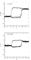
- FIG. 7 is a magnetization curve of the sample of Demonstration Example 1, where the horizontal axis is the external magnetic field H(Oe) and the vertical axis is M/Ms.
- One of the magnetization curves is when the external magnetic field is a perpendicular magnetic field, and the other is when the external magnetic field is an in-plane magnetic field.
- a perpendicular magnetic field was applied, it was found that antiferromagnetic coupling occurred at zero magnetic field.
- FIG. 8 is a magnetization curve of the sample of Demonstration Example 2, where the horizontal axis is the external magnetic field H(Oe) and the vertical axis is the magnetization M/Ms.
- One of the magnetization curves is when the external magnetic field is a perpendicular magnetic field, and the other is when the external magnetic field is an in-plane magnetic field. When a perpendicular magnetic field was applied, it was found that antiferromagnetic coupling occurred at zero magnetic field.
- FIG. 9 is a magnetization curve of the sample of Demonstration Example 3, where the horizontal axis is the external magnetic field H(Oe) and the vertical axis is M/Ms.
- One of the magnetization curves is when the external magnetic field is a perpendicular magnetic field, and the other is when the external magnetic field is an in-plane magnetic field. It was found that antiferromagnetic coupling occurred when a vertical magnetic field was applied.
- the thickness t_Ir of the Ir layer is set to 0.5 nm, 0.55 nm, and 1.4 nm, and the sum of the thicknesses of the Pt layer and the Ir layer, that is, the total thickness of the non-magnetic layers is adjusted within the range of 0.5 to 2.5 nm. did.
- the non-magnetic layer may be Ir/Pt, Pt/Ir/Pt, or only an Ir layer. The case of only the Ir layer is performed as a comparative example. When the Pt layers were provided above and below the Ir layer, the upper and lower Pt layers were made to have the same thickness.
- FIG. 10 is a graph showing the dependence of the interlayer coupling force J ex (mJ/m 2 ) on the total thickness t total (nm) of the non-magnetic layers. From FIG. 10, it can be seen that by inserting a Pt layer into the Co/Ir/Co stack, the interlayer coupling force J ex , which indicates the magnitude of the Ir antiferromagnetic coupling, monotonically was found to decrease to In addition, even if the total thickness of Pt/Ir/Pt is 2.5 nm, it should be confirmed that the antiferromagnetic coupling is established, and the total thickness of Pt/Ir/Pt should be 1.5 to 2.5 nm. It has become clear that an antiferromagnetically coupled film can be continuously produced over a wide range of 5 nm. This indicates that the RKKY interaction propagates in Pt, but the RKKY oscillation does not occur.
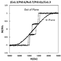
- FIG. 11 is a magnetization curve of the sample of Demonstration Example 5, where the horizontal axis is the external magnetic field H(Oe) and the vertical axis is M/Ms. Ms is the saturation magnetization.
- One of the magnetization curves is when the external magnetic field is a perpendicular magnetic field, and the other is when the external magnetic field is an in-plane magnetic field. When a perpendicular magnetic field was applied, it was found that antiferromagnetic coupling occurred at zero magnetic field.
- FIG. 12 is a magnetization curve of the sample of Demonstration Example 6, where the horizontal axis is the external magnetic field H(Oe) and the vertical axis is M/Ms. Ms is the saturation magnetization.
- One of the magnetization curves is when the external magnetic field is a perpendicular magnetic field, and the other is when the external magnetic field is an in-plane magnetic field. When a perpendicular magnetic field was applied, it was found that antiferromagnetic coupling occurred at zero magnetic field.
- FIG. 13 is a magnetization curve of the sample of Demonstration Example 7, where the horizontal axis is the external magnetic field H(Oe) and the vertical axis is M/Ms. Ms is the saturation magnetization.
- One of the magnetization curves is when the external magnetic field is a perpendicular magnetic field, and the other is when the external magnetic field is an in-plane magnetic field. When a perpendicular magnetic field was applied, it was found that antiferromagnetic coupling occurred at zero magnetic field.
- FIG. 14 is a magnetization curve of the sample of Demonstration Example 8, where the horizontal axis is the external magnetic field H(Oe) and the vertical axis is M/Ms. Ms is the saturation magnetization.
- One of the magnetization curves is when the external magnetic field is a perpendicular magnetic field, and the other is when the external magnetic field is an in-plane magnetic field. When a perpendicular magnetic field was applied, it was found that antiferromagnetic coupling occurred at zero magnetic field.
- an antiferromagnetic coupling layer consisting of a Pt layer, a Ru layer, and a Pt layer between the upper and lower Co layers as described above, the magnetization of one Co layer is changed to the magnetization direction of the other Co layer. It turned out to be the other way around.
- the thickness t_Ru of the Ru layer is set to 0.4 nm, 0.7 nm, and 0.8 nm, and the sum of the thicknesses of the Pt layer and the Ru layer, that is, the total thickness of the non-magnetic layers is adjusted within the range of 0.4 to 2.3 nm. did.
- the non-magnetic layer may be Ru/Pt, Pt/Ru/Pt, or Ru layer only. The case of only the Ru layer is performed as a comparative example. When the Pt layers were provided above and below the Ru layer, the upper and lower Pt layers were made to have the same thickness.
- FIG. 15 is a graph showing the dependence of the interlayer coupling force J ex (mJ/m 2 ) on the total thickness t total (nm) of the non-magnetic layers. From FIG. 15, by inserting the Pt layer into the Co/Ru/Co stack, the interlayer coupling force Jex , which indicates the magnitude of the antiferromagnetic coupling of Ru, monotonously increases as the thickness of the nonmagnetic layer increases. was found to be decreasing. It was also confirmed that antiferromagnetic coupling was achieved even when the total film thickness of Pt/Ru/Pt was 2.3 nm.
- the antiferromagnetic coupling film can be continuously formed over a wide range of Pt/Ir/Pt total thicknesses ranging from 1.3 to 2.3 nm. It also shows that the RKKY interaction propagates in Pt, but the RKKY oscillation does not occur.
- FIG. 16 shows the Ir thickness dependence of the interlayer bonding strength J ex .
- the horizontal axis is the Ir thickness (nm), and the vertical axis is the interlayer bonding strength Jex .
- the bullet plot relates to (Co/Pt) 4.5 /Ir/(Co/Pt) 4.5 and the diamond plot relates to (Co/Pt/Ir) 2 /Co.
- the thickness t Ir of the Ir layer in each plot is 0.4 nm, 0.5 nm, 0.6 nm, 0.7 nm, 0.8 nm, 0.9 nm, 1.0 nm, 1.1 nm, 1.2 nm, 1.3 nm.
- the thickness of the Ir layer is preferably in the range of 0.4 nm to 0.7 nm and 1.3 nm to 1.6 nm.
- FIG. 17 shows Ru thickness dependence of the interlayer bonding force J ex .
- the horizontal axis is the Ru thickness (nm), and the vertical axis is the interlayer bonding strength Jex .
- the bullet plots relate to (Co/Pt/Ru) 2 /Co and the diamond plots relate to (Co/Pt) 4.5 /Ru/(Co/Pt) 4.5 .
- the Ru layer thickness t Ru in each plot is 0.4 nm, 0.5 nm, 0.6 nm, 0.7 nm, 0.8 nm, 0.9 nm, 1.0 nm, 1.1 nm, 1.2 nm, 1.4 nm.
- the thickness of Ru should be selected so as to give the 2nd peak of the interlayer bonding strength J ex . It was found that the thickness of the Ru layer is preferably in the range of 0.6 nm to 0.9 nm and 1.7 nm to 2.2 nm.
- FIG. 18 is a diagram schematically showing a Hall bar and a measurement system produced as sample 29.
- FIG. FIG. 19A is a cross-sectional view of the fabricated sample 29.
- FIG. Sample 29, as shown in FIG. 19A includes a Si substrate 101 provided with a thermal oxide film, a Ta layer 102 having a thickness of 2.0 nm provided on the thermal oxide film, and a Ta layer 102 having a thickness of 2.0 nm.
- FIG. 19B is a cross-sectional view of the manufactured sample in Comparative Example 2.
- FIG. Another comparative sample as shown in FIG. A Pt layer 123 with a thickness of 7.2 nm, a Co layer 124 with a thickness of 1.3 nm provided on the Pt layer 123, an Ir layer 125 with a thickness of 0.6 nm provided on the Co layer 124, and the Ir layer 125 It was composed of a Pt layer 126 with a thickness of 0.6 nm provided thereon and a Ta layer 127 with a thickness of 3.0 nm provided on the Pt layer 126 .
- FIG. 20 is a diagram showing the pulse current dependence of the Hall resistance Rxy ( ⁇ ) of Sample 29 and Comparative Example 2.
- FIG. The horizontal axis is the pulse current I (mA), and the vertical axis is the Hall resistance Rxy ( ⁇ ).
- the Hall resistance Rxy increased at a certain current value
- the Hall resistance Rxy decreased at a certain current value. It was found that the magnetization was reversed.
- the write current (reversal current) when using the Co/Pt/Ir/Pt/Co antiferromagnetically coupled film is It was found that the write current (reversal current) of As a result, it was found that the energy during writing was also reduced to about 1/4.
- Samples 30 to 34 are, as shown in FIG. Ir layer 103 with a thickness of 2.0 nm, Co layer 104 with a thickness of 1.1 nm provided on the Ir layer 103, Pt layer 105 with a thickness of 0.6 nm provided on the Co layer 104, and Pt layer 105 an Ir layer 106 having a predetermined thickness provided thereon; a Pt layer 107 having a thickness of 0.6 nm provided on the Ir layer 106; a Co layer 108 having a thickness of 1.1 nm provided on the Pt layer 107; A 0.5 nm thick Ir layer 109 provided on the layer 108, a 1.5 nm thick MgO layer 110 provided on the Ir layer 109, and a 1.0 nm thick Ta layer provided on the MgO layer 110. 111.
- the thickness of the Ir layer 106 was 0.5 nm for sample 30,
- FIG. 21A is a diagram showing the dependence of the spin generation efficiency on the Ir layer thickness for Samples 30 to 34
- FIG. 21B is the interlayer coupling force J ex (mJ/m 2 ) dependence of the spin generation efficiency for Samples 30 to 34. It is a figure which shows.
- the horizontal axis of FIG. 21A is the Ir thickness t_Ir (nm)
- the horizontal axis of FIG. 21B is the interlayer coupling force J ex (mJ/m 2 )
- the vertical axis of FIGS. %) In FIGS.
- a multilayer film of (Pt 1.0 nm/Ir 0.8 nm) 4 and a Pt layer with a thickness of 7.2 nm are shown as comparative examples. The results for the case are also shown.
- the spin generation efficiency ⁇ SH (%) increases as the thickness of the Ir layer decreases from 0.6 nm to 0.5 nm.
- ⁇ SH ( %) is inversely proportional to the write current (reversal current) and power consumption. It was found that the inversion current can be reduced to about 1/5 and the power consumption can be reduced to about 1/25 compared to Sample 2). From this result, it was found that the power consumption can be reduced as the interlayer bonding strength J ex (mJ/m 2 ) increases.
- the thickness of the Ir layer is preferably 0.4 nm or more and 0.6 nm or less. , more preferably 0.50 nm or more and 0.58 nm or less.
- Samples 35 to 39 are, as shown in FIG. Ir layer 103 with a thickness of 2.0 nm, Co layer 104 with a thickness of 1.1 nm provided on the Ir layer 103, Pt layer 105 with a predetermined thickness provided on the Co layer 104, and on the Pt layer 105
- An Ir layer 106 with a thickness of 0.5 nm provided, a Pt layer 107 with a predetermined thickness provided on the Ir layer 106, a Co layer 108 with a thickness of 1.1 nm provided on the Pt layer 107, and a Co layer 108
- An Ir layer 109 with a thickness of 0.5 nm provided thereon, an MgO layer 110 with a thickness of 1.5 nm provided on the Ir layer 109, and a Ta layer 111 with a thickness of 1.0 nm provided on the MgO layer 110 It consisted of The thicknesses of
- FIG. 22A is a diagram showing the Pt layer thickness dependence of the spin generation efficiency for Samples 35 to 39
- FIG. 22B is the interlayer coupling force J ex (mJ/m 2 ) dependence of the spin generation efficiency for Samples 35 to 39. It is a figure which shows.
- the horizontal axis of FIG. 22A is the total thickness t_Pt (nm) of the Pt layers 145 and 147
- the horizontal axis of FIG. 22B is the interlayer bonding strength J ex (mJ/m 2 )
- the axis is the spin generation efficiency ⁇ SH (%).
- 22A and 22B show the case of a multilayer film of (Pt 1.0 nm/Ir 0.8 nm) 4 and a Pt layer with a thickness of 7.2 nm as comparative examples instead of the Pt layer 145/Ir layer 146/Pt layer 147.
- the results for the case of are also shown.
- the thickness of the Pt layer increases from 0.8 nm to about 1.3 nm, the spin generation efficiency ⁇ SH (%) increases, and when the thickness of the Pt layer increases from about 1.3 nm to 1.6 nm, the spin generation efficiency ⁇ SH (%) decreases.
- the thickness of the Pt layer is such that the spin Hall angle and the spin generation efficiency are maximized.
- the thickness of the Pt layer is in the above range ( Pt 1.0 nm/Ir 0.8 nm). Spin generation efficiency is relatively high.
- the thickness of the Pt layers 105 and 107 is preferably 0.4 nm or more and 0.8 nm or less, more preferably about 0.5 nm or more and about 0.8 nm or less, and particularly preferably 0.55 nm or more and 0.75 nm or less.
- the conductive layer 50 as the magnetic laminated film according to the fifth embodiment is the antiferromagnetic coupling layer 10a of the second ferromagnetic layers 16 and 45 in the magnetic laminated films 10 and 40 according to the first to fourth embodiments.
- 40a is provided with a third nonmagnetic layer 61, and the third nonmagnetic layer 61 is a metal or alloy containing at least one of W, Cu, Ta, and Mn (W alloy, Cu alloy, Ta alloy, Mn alloy, MnIr alloy, TaW alloy).
- the magnetoresistive effect element 5 according to the fifth embodiment is the second ferromagnetic layers 16 and 45 in the magnetic laminated films 10 and 40 according to the magnetoresistive effect elements 1 to 4 according to the first to fourth embodiments.
- a third nonmagnetic layer (for example, the third nonmagnetic layer 61 shown in FIG. 23B) is provided on the side of the recording layers 17, 28, 28A, which is the opposite surface of the antiferromagnetic coupling layers 10a, 40a. Therefore, the items described in the first to fourth embodiments, the material and thickness of each layer, etc. are omitted to avoid redundant description, and the case of applying to the form shown in FIG. 1B will be described below as a representative. A person skilled in the art will not need a description of the cases applied to the second to fourth embodiments.
- FIG. 23A is a plan view of a magnetoresistive element according to the fifth embodiment
- FIG. 23B is a cross-sectional view taken along line EE in FIG. 23A.
- the magnetoresistive element 5 according to the fifth embodiment includes an underlayer 51 provided on a substrate (not shown), a first ferromagnetic layer 52 provided on the underlayer 51, and a first ferromagnetic layer 52 provided on the underlayer 51.
- 55 and a second ferromagnetic layer 56 provided on the second nonmagnetic layer 55 .
- the conductive layer 50 is configured as follows. A first nonmagnetic layer 53 and a second nonmagnetic layer 55 are in contact with the corresponding upper and lower surfaces of the interlayer coupling layer 54 to sandwich the interlayer coupling layer 54 to form an antiferromagnetic coupling layer 50a.
- the ferromagnetic layer 52 is in contact with the lower surface of the first nonmagnetic layer 53, and the second ferromagnetic layer 56 is in contact with the upper surface of the second nonmagnetic layer 55, so that the first ferromagnetic layer 52 and a second ferromagnetic layer 56 sandwich a first nonmagnetic layer 53, an interlayer coupling layer 54 and a second nonmagnetic layer 55, and a third nonmagnetic layer is formed on the second ferromagnetic layer 56.
- 61, and the third nonmagnetic layer 61 is a metal or alloy containing at least one of W, Cu, Ta, and Mn (W alloy, Cu alloy, Ta alloy, Mn alloy, MnIr alloy, TaW alloy ).
- the third non-magnetic layer 61 can be in contact with the top surface of the second ferromagnetic layer 56 and the bottom surface of the recording layer 57 .
- the second ferromagnetic layer 56 with which the third nonmagnetic layer 61 is in contact has magnetization tilted with respect to the current direction of the conductive layer 50, that is, it has a z-direction component.
- the third non-magnetic layer 61 preferably has a thickness of 0.3 nm or more and 2.0 nm or less after the magnetoresistive element 5 is formed (junction separation).
- a recording layer 57 made of a material capable of reversing magnetization is formed on the third non-magnetic layer 61, and a barrier layer 58 is provided on the recording layer 57 so as to be in contact therewith. ing.
- a non-magnetic layer 59 is provided on the barrier layer 58 as a reference layer.
- the magnetoresistive element 5 using the tunnel anisotropic magnetoresistive effect is configured by stacking a recording layer 57, a barrier layer 58, and a nonmagnetic layer 59.
- a second nonmagnetic layer (a layer made of a metal or alloy containing Pt) 55 and a third nonmagnetic layer (W, Cu, Ta, A layer made of a metal or alloy (W alloy, Cu alloy, Ta alloy, Mn alloy, MnIr alloy, TaW alloy) containing any of Mn) 61 is different.
- a Co layer as the second ferromagnetic layer 56 may be used as the second nonmagnetic layer (a layer made of a metal or alloy containing Pt) 55 and a third nonmagnetic layer (any of W, Cu, Ta, and Mn).
- first ferromagnetic layer 52 and the second ferromagnetic layer 56 are magnetized so as to have a perpendicular component, by passing a current through the conductive layer 50, The magnetization of the first ferromagnetic layer 52 and the second ferromagnetic layer 56 can be reversed even with zero external magnetic field.
- a metal or alloy W alloy, Cu alloy, Ta alloy, Mn alloy, MnIr alloy, TaW alloy
- Co/Pt and any one of Co/W, Co/Cu, Co/Ta, and Co/Mn have opposite signs of magnetic field interacting with each other.
- the magnetic field is applied in the same direction as indicated by reference numerals 66 and 67, and the spin of the second ferromagnetic layer 56 is tilted in the X direction.
- This magnetic field is considered the DM interaction magnetic field (H DMI ) resulting from the Dzyaloshinskii-Moriya (DM) interaction, the magnetic fields 66, 67 being the H DMI .
- the recording layer 17 in FIG. 23B, It is provided on the recording layer 57) side, for example, between the second ferromagnetic layer 16 and the recording layer 17 (between the second ferromagnetic layer 56 and the recording layer 57 in FIG. 23B).
- the third nonmagnetic layer 61 is placed on the recording layer 28, 28A side so as to face the magnetic laminated film 10, for example, as shown in FIG. It is provided between the second ferromagnetic layer 16 and the non-magnetic layer 27 shown in FIG. 3C or between the second ferromagnetic layer 16 and the recording layer 28A shown in FIG. 3D.
- the third non-magnetic layer 61 is arranged on the recording layer 17 side so as to face the magnetic laminated film 40, for example, as shown in FIG. 4B. 2 between the ferromagnetic layer 45 and the recording layer 17 .
- the third non-magnetic layer 61 is placed on the side of the recording layers 28 and 28A so as to face the magnetic laminated film 40, for example, as shown in FIG. It is provided between the second ferromagnetic layer 45 and the non-magnetic layer 27 shown in FIG. 6C or, for example, between the second ferromagnetic layer 45 and the recording layer 28A shown in FIG. 6D.
- the conductive layer 50 as the magnetic laminated film according to the sixth embodiment is the antiferromagnetic coupling layer 10a of the first ferromagnetic layers 12 and 42 in the magnetic laminated films 10 and 40 according to the first to fourth embodiments.
- 40a is provided with a third nonmagnetic layer 61, and the third nonmagnetic layer 61 is a metal or alloy containing at least one of W, Cu, Ta, and Mn (W alloy, Cu alloy, Ta alloy, Mn alloy, MnIr alloy, TaW alloy).
- the magnetoresistive effect element 6 according to the sixth embodiment is composed of the first ferromagnetic layers 12 and 42 in the magnetic laminated films 10 and 40 according to the magnetoresistive effect elements 1 to 4 according to the first to fourth embodiments.
- a third nonmagnetic layer (for example, the third nonmagnetic layer 61 shown in FIG. 24) is provided on the opposite side of the recording layer, which is the opposite side of the antiferromagnetic coupling layers 10a and 40a. Therefore, the items described in the first to fourth embodiments, the material and thickness of each layer, etc. are omitted to avoid redundant description, and the case of applying to the form shown in FIG. 1B will be described below as a representative. A person skilled in the art will not need a description of the cases applied to the second to fourth embodiments.
- FIG. 24 is a cross-sectional view of a magnetoresistive element according to the sixth embodiment. A plan view is omitted because it is the same as FIG. 23A. Also in the sixth embodiment, the first non-magnetic layer 53 and the second non-magnetic layer 55 are in contact with the corresponding upper and lower surfaces of the interlayer coupling layer 54, sandwiching the interlayer coupling layer 54 between the antiferromagnetic coupling layers 50a. A third nonmagnetic layer 61 is provided on the lower surface of the conductive layer 50, which is the surface of the first ferromagnetic layer 52 opposite to the antiferromagnetic coupling layer 50a.
- the third nonmagnetic layer 61 is a layer made of a metal or alloy (W alloy, Cu alloy, Ta alloy, Mn alloy, MnIr alloy, TaW alloy) containing W, Cu, Ta, or Mn.
- the third nonmagnetic layer 61 may contact the top surface of the underlayer 51 and the bottom surface of the first ferromagnetic layer 52 .
- the magnetization of the first ferromagnetic layer 52 and the second ferromagnetic layer 56 is tilted with respect to the current direction of the conductive layer 50, that is, has a z-direction component.
- the third nonmagnetic layer 61 When the third nonmagnetic layer 61 is provided in contact with the lower surface of the first ferromagnetic layer 52, there is no particular limitation on the thickness, but in order to maintain antiferromagnetic coupling, the first ferromagnetic layer 52, the first It is essential that the nonmagnetic layer 53, the second nonmagnetic layer 55, and the second ferromagnetic layer 56 maintain the fcc (111) orientation. In that sense, it is most preferable to use Cu in this case.
- the third nonmagnetic layer 61 preferably has a thickness of 0.3 nm or more and 2.0 nm or less.
- a first nonmagnetic layer (a layer made of a metal or alloy containing Pt) 53 and a third nonmagnetic layer (W, Cu, Ta, A layer made of a metal or alloy (W alloy, Cu alloy, Ta alloy, Mn alloy, MnIr alloy, TaW alloy) containing any of Mn) 61 is different.
- a Co layer as the first ferromagnetic layer 52 is combined with a first nonmagnetic layer (a layer made of a metal or alloy containing Pt) 53 and a third nonmagnetic layer (any of W, Cu, Ta, and Mn).
- first ferromagnetic layer 52 and the second ferromagnetic layer 56 are magnetized so as to have a perpendicular component, by passing a current through the conductive layer 50, The magnetization of the first ferromagnetic layer 52 and the second ferromagnetic layer 56 can be reversed even with zero external magnetic field.
- a metal or alloy W alloy, Cu alloy, Ta alloy, Mn alloy, MnIr alloy, TaW alloy
- Co/Pt interacts with any one of Co/W, Co/Cu, Co/Ta, and Co/Mn because the magnetic fields interacting with each other have opposite signs.
- the magnetic field is applied in the same direction as indicated by reference numerals 66 and 67, and the spin of the second ferromagnetic layer 56 is tilted in the X direction.
- This magnetic field can be considered as the DM interaction magnetic field (HDMI) resulting from the Dzyaloshinskii -Moriya (DM) interaction, the magnetic fields 66, 67 being the HDMI.
- HDMI Dzyaloshinskii -Moriya
- the recording layer 17 in FIG. 24, provided on the opposite side of the recording layer 57, for example, between the underlayer 11 and the first ferromagnetic layer 12 shown in FIG. 1B (between the second ferromagnetic layer 56 and the recording layer 57 in FIG. 24). be done.
- the third nonmagnetic layer 61 is arranged on the side opposite to the recording layer 17 so as to face the magnetic laminated film 10, for example, as shown in FIGS. It is provided between the underlayer 11 and the first ferromagnetic layer 12 shown in FIGS. 3C and 3D.
- the third nonmagnetic layer 61 is arranged on the opposite side of the recording layer 17 so as to face the magnetic laminated film 40, for example, as shown in FIG. 4B. It is provided between the shown underlying layer 41 and the first ferromagnetic layer 42 .
- the third non-magnetic layer 61 is placed on the side of the recording layers 28 and 28A so as to face the magnetic laminated film 40, for example, as shown in FIG. It is provided between the second ferromagnetic layer 45 and the non-magnetic layer 27 shown in FIG. 6C or between the second ferromagnetic layer 45 and the recording layer 28A shown in FIG. 6D.
- the conductive layer 50 as the magnetic laminated film according to the seventh embodiment is the antiferromagnetic coupling layer 10a of the first ferromagnetic layers 12 and 42 in the magnetic laminated films 10 and 40 according to the first to fourth embodiments.
- 40a, and a fourth nonmagnetic layer 62 is provided on the surface of the second ferromagnetic layers 16, 45 opposite to the antiferromagnetic coupling layers 10a, 40a.
- the third nonmagnetic layer 61 and the fourth nonmagnetic layer 62 are made of metal or alloy (W alloy, Cu alloy, Ta alloy, Mn alloy, MnIr alloy, TaW alloy).
- the magnetoresistive element 7 according to the seventh embodiment is the anti-reflection of the first ferromagnetic layers 12 and 42 in the magnetic laminated films 10 and 40 of the magnetoresistive elements 1 to 4 according to the first to fourth embodiments.
- a third nonmagnetic layer (for example, the third nonmagnetic layer 61 shown in FIG. 25) is provided on the side opposite to the recording layer on the side opposite to the ferromagnetic coupling layers 10a and 40a, and the second ferromagnetic layer 16,
- a fourth nonmagnetic layer (for example, the fourth nonmagnetic layer 62 shown in FIG. 25) is provided on the surface of 45 opposite to the antiferromagnetic coupling layers 10a and 40a.
- FIG. 25 is a cross-sectional view of a magnetoresistive element according to the seventh embodiment. A plan view is omitted because it is the same as FIG. 23A.
- the conductive layer 50 includes a first nonmagnetic layer 53, an interlayer coupling layer 54, and a second nonmagnetic layer 55, which constitute an antiferromagnetic coupling layer 50a.
- a third non-magnetic layer (metal or alloy containing any of W, Cu, Ta, Mn (W alloy, Cu alloy, Ta alloy, Mn alloy, MnIr alloy, and TaW alloy))) 61, and a fourth nonmagnetic layer (W, A layer 62 made of a metal or alloy (W alloy, Cu alloy, Ta alloy, Mn alloy, MnIr alloy, TaW alloy) containing Cu, Ta, or Mn.
- the magnetization of the first ferromagnetic layer 52 and the second ferromagnetic layer 56 is tilted with respect to the current direction of the conductive layer 50, that is, has a z-direction component.
- the fourth non-magnetic layer (a layer made of any metal or alloy of W, Cu, Ta, Mn (W alloy, Cu alloy, Ta alloy, Mn alloy, MnIr alloy, TaW alloy)) 62 has a magnetoresistive effect It preferably has a thickness of 0.3 nm or more and 2.0 nm or less after the element 7 is formed (junction isolation). Unless W, Cu, Ta, and Mn remain on the second ferromagnetic layer 56 after junction separation, magnetization reversal in the absence of a magnetic field described below cannot be observed. When the magnetic interaction between the first ferromagnetic layer 52 and the second ferromagnetic layer 56 is SOT magnetized, the recording layer 57 of the magnetoresistive element 7 is also magnetized.
- the third non-magnetic layer (a layer made of a metal or alloy containing W, Cu, Ta, or Mn (W alloy, Cu alloy, Ta alloy, Mn alloy, MnIr alloy, TaW alloy)) 61 has a thickness
- the first ferromagnetic layer 52, the first nonmagnetic layer 53, the second nonmagnetic layer 55, and the second ferromagnetic layer 56 are fcc (111) Maintaining the orientation is essential. In that sense, it is most preferable to use Cu in this case.
- the third nonmagnetic layer 61 and the fourth nonmagnetic layer 62 are made of different materials.
- the third nonmagnetic layer 61 preferably has a thickness of 0.3 nm or more and 2.0 nm or less.
- a first nonmagnetic layer (a layer made of a metal or alloy containing Pt) 53 and a third nonmagnetic layer (W, Cu, Ta, A layer made of a metal or alloy (W alloy, Cu alloy, Ta alloy, Mn alloy, MnIr alloy, TaW alloy) containing any of Mn) 61 is different.
- a layer made of an alloy (W alloy, Cu alloy, Ta alloy, Mn alloy, MnIr alloy, TaW alloy)) 62 is different.
- the first ferromagnetic layer 52 and the second ferromagnetic layer 56 are magnetized to have a perpendicular component without applying an external magnetic field. Even if the current is applied to the conductive layer 50, the magnetization of the first ferromagnetic layer 52 and the second ferromagnetic layer 56 can be reversed even when the external magnetic field is zero.
- the third nonmagnetic layer 61 is arranged on the side opposite to the recording layer 17 so as to face the magnetic laminated film 10, for example, as shown in FIGS.
- the recording layers 28 and 28A are provided between the underlayer 11 and the first ferromagnetic layer 12 shown in FIGS. 3C and 3D so that the fourth nonmagnetic layer 62 faces the magnetic laminated film 10 side, for example between the second ferromagnetic layer 16 and the non-magnetic layer 27 shown in FIGS. 3B and 3C or between the second ferromagnetic layer 16 and the recording layer 28A shown in FIG. 3D. ing.
- the third nonmagnetic layer 61 is arranged on the opposite side of the recording layer 17 so as to face the magnetic laminated film 40, for example, as shown in FIG. 4B.
- the fourth non-magnetic layer 62 is provided between the underlayer 41 and the first ferromagnetic layer 42 shown in FIG. is provided between the second ferromagnetic layer 45 and the recording layer 17 shown in FIG.
- the third nonmagnetic layer 61 is arranged on the opposite side of the recording layer 28 so as to face the magnetic laminated film 40, for example, as shown in FIG. 6B.
- the fourth non-magnetic layer 62 is provided between the underlayer 41 and the first ferromagnetic layer 42 shown in FIG. 6C, or between the second ferromagnetic layer 45 and the recording layer 28A shown in FIG. 6D.
- the magnetoresistive element 1 of the first to fourth embodiments between the first ferromagnetic layers 12, 42 and the magnetic laminated films 10, 40, the second A metal or alloy (W alloy, Cu alloy, Ta alloy, Mn A third non-magnetic layer 61 and a fourth non-magnetic layer 62 are interposed.
- the third nonmagnetic layer 61 and the fourth nonmagnetic layer 62 can also be called a magnetic laminated film.
- FIG. 10 is a cross-sectional view of Demonstration Example 10.
- FIG. 10 In Demonstration Example 10, as shown in FIG.
- FIG. 27 is an electron microscope image of the Hall bar produced in Demonstration Example 10, and the right side is an enlarged image of the center of the image.
- 28A to 28F are diagrams showing the pulse current dependence of Hall resistance Rxy( ⁇ ) in Demonstration Example 10.
- FIG. The horizontal axis is the pulse current I (A), and the vertical axis is the Hall resistance Rxy ( ⁇ ).
- the Hall resistance Rxy decreases at a certain current value when the pulse current is applied in the + direction, and the Hall resistance Rxy decreases at a certain current value when the pulse current is applied in the - direction. Since the increase was observed, it was found that the magnetic moments of the Co layers 144 and 148 were reversed by the pulsed current.
- H DMI DM interaction magnetic field
- FIG. 29 is a diagram showing the dependence of the Hall resistance Rxy (Ohm) on the number of repetitions when pulse currents are alternately applied in ⁇ directions in no magnetic field in Demonstration Example 10. From FIG. 29, it was found that stable magnetization reversal occurred even when the application of the pulse current in the ⁇ directions was repeated.
- a Hall bar was produced in the same manner as in FIGS. 18 and 26, and a measurement system was constructed.
- An Ir layer 143 with a thickness of 2.0 nm, a Co layer 144 with a thickness of 1.1 nm provided on the Ir layer 143, a Pt layer 145 with a thickness of 0.6 nm provided on the Co layer 144, and on the Pt layer 145 A 0.5 nm thick Ir layer 146 provided on the Ir layer 146, a 0.6 nm thick Pt layer 147 provided on the Ir layer 146, a 1.1 nm thick Co layer 148 provided on the Pt layer 147, A Cu layer 149 with a thickness of 1.0 nm provided on the Co layer 148, an MgO layer 150 with a thickness of 1.5 nm provided on the Cu layer 149, and a Ta layer with a thickness of 1.0 nm provided on the MgO layer 150 layer
- FIG. 30 is a diagram showing the results of the pulse current dependence of the Hall resistance Rxy ( ⁇ ) in Demonstration Example 11 when the pulse current I was applied for 200 ⁇ s and a constant external magnetic field Hex was not applied during measurement. be.
- the horizontal axis is the pulse current I (mA), and the vertical axis is the Hall resistance Rxy ( ⁇ ).
- FIG. 31 is a diagram showing the dependence of the Hall resistance Rxy (Ohm) on the number of repetitions when pulse currents are alternately applied in ⁇ directions in no magnetic field in Demonstration Example 11.
- Rxy Hall resistance
- a Hall bar was produced in the same manner as in Fig. 18, and a measurement system was constructed.
- An Ir layer 163 with a thickness of 2.0 nm, a Cu layer 164 with a thickness of 1.0 mm provided on the Ir layer 163, a Co layer 165 with a thickness of 1.1 nm provided on the Cu layer 164, and on the Co layer 165 A Pt layer 166 with a thickness of 0.6 nm provided on the Pt layer 166, an Ir layer 167 with a thickness of 0.55 nm provided on the Pt layer 166, a Pt layer 168 with a thickness of 0.6 nm provided on the Ir layer 167, A Co layer 169 with a thickness of 1.1 nm provided on the Pt layer 168, a W layer 170 with a thickness of 1.0 nm provided on the Co layer 169, and MgO with a thickness of 1.5 nm provided on the
- FIG. 33 is a diagram showing pulse current dependence of Hall resistance Rxy( ⁇ ) in Demonstration Example 12.
- the horizontal axis is the pulse current I (A), and the vertical axis is the Hall resistance Rxy ( ⁇ ).
- a pulse current I was applied for 200 ⁇ s and no constant external magnetic field Hex was applied. From FIG.
- a Hall bar was produced in the same manner as in FIGS. 18 and 26, and a measurement system was constructed.
- An Ir layer 143 with a thickness of 2.0 nm, a Co layer 144 with a thickness of 1.1 nm provided on the Ir layer 143, a Pt layer 145 with a thickness of 0.6 nm provided on the Co layer 144, and on the Pt layer 145 A 0.55 nm thick Ir layer 146 provided on the Ir layer 146, a 0.6 nm thick Pt layer 147 provided on the Ir layer 146, a 1.1 nm thick Co layer 148 provided on the Pt layer 147, A W layer 149 with a thickness of 0.7 nm provided on the Co layer 148, an MgO layer 150 with a thickness of 1.5 nm provided on the W layer 149, and a Ta layer with a thickness of 1.0 nm provided on the MgO layer 150.
- FIG. 34 is a diagram showing pulse current dependence of Hall resistance Rxy( ⁇ ) in Demonstration Example 13.
- the horizontal axis is the pulse current I (A), and the vertical axis is the Hall resistance Rxy ( ⁇ ).
- a pulse current I was applied for 200 ⁇ s and no constant external magnetic field Hex was applied. From FIG.
- FIG. 35 is a diagram showing pulse current dependence of the Hall resistance Rxy ( ⁇ ) in Demonstration Example 14.
- the horizontal axis is the pulse current I (A), and the vertical axis is the Hall resistance Rxy ( ⁇ ).
- a pulse current I was applied for 200 ⁇ s and no constant external magnetic field Hex was applied. From FIG. 35, it was observed that when the pulse current was applied in the + direction, the Hall resistance Rxy increased at a certain current value, and when it was applied in the - direction, the Hall resistance Rxy decreased at a certain current value. It was found that the magnetic moment was reversed by the pulsed current.
- FIG. 36 is a diagram showing pulse current dependence of Hall resistance Rxy ( ⁇ ) in Demonstration Example 15.
- FIG. The horizontal axis is the pulse current I (A), and the vertical axis is the Hall resistance Rxy ( ⁇ ).
- a pulse current I was applied for 200 ⁇ s and no constant external magnetic field Hex was applied. From FIG. 36, it was observed that the Hall resistance Rxy decreased at a certain current value when the pulse current was applied in the + direction, and the Hall resistance Rxy increased at a certain current value when the pulse current was applied in the ⁇ direction. It was found that the magnetic moment was reversed by the pulsed current.
- a Hall bar was produced in the same manner as in FIGS. 18 and 26, and a measurement system was constructed.
- the W layer 129 with a thickness of 0.7 nm was used in Demonstration Example 13, but in Demonstration Example 16, the Ir 22 Mn 78 layer 129 with a thickness of 2.0 nm was used.
- the pulse current I was passed in the y direction, and the Hall voltage V was measured.
- FIG. 37 is a diagram showing pulse current dependence of the Hall resistance Rxy( ⁇ ) in Demonstration Example 16.
- FIG. The horizontal axis is the pulse current I (A), and the vertical axis is the Hall resistance Rxy ( ⁇ ).
- a pulse current I was applied for 200 ⁇ s and no constant external magnetic field Hex was applied. From FIG. 37, it was observed that when the pulse current was applied in the + direction, the Hall resistance Rxy increased at a certain current value, and when the pulse current was applied in the - direction, the Hall resistance Rxy decreased at a certain current value. It was found that the magnetic moment was reversed by the pulsed current.
- FIG. 38 is a diagram showing the dependence of the Hall resistance Rxy (Ohm) on the number of repetitions when pulse currents are alternately applied in ⁇ directions in no magnetic field in Demonstration Example 16.
- Rxy Hall resistance
- FIG. 39 is a graph showing pulse current dependence of Hall resistance Rxy ( ⁇ ) in Comparative Example 3. FIG. The horizontal axis is the pulse current I (A), and the vertical axis is the Hall resistance Rxy ( ⁇ ).
- Comparative Example 4 a Hall bar was produced in the same manner as in FIG. 18, and a measurement system was constructed. 40 is a cross-sectional view of Comparative Example 4.
- FIG. 4 a Si substrate 181 provided with a thermally oxidized film, a Ta layer 182 having a thickness of 3 nm provided on the thermally oxidized film, and a Pt layer having a thickness of 1.0 nm provided on the Ta layer 182.
- a stack 183 (total film thickness: 7.2 nm) with an Ir layer of 0.8 nm, a Co layer 184 with a thickness of 1.3 nm provided on the stack 183, and a It was composed of a W layer 185 , a 1.5 nm thick MgO layer 186 provided on the W layer 185 , and a 1.0 nm thick Ta layer 187 provided on the MgO layer 186 .
- At least one of W, Cu, Ta, and Mn metals or alloys may be provided on the surface opposite to the antiferromagnetic coupling layer 50a of the first ferromagnetic layer 52 in FIG.
- a third non-magnetic layer 61 made of at least one of W, Cu, Ta, and Mn metals or alloys (W alloy, Cu alloy, Ta alloy, Mn alloy, MnIr alloy, TaW alloy) is provided, or At least one of W, Cu, Ta, and Mn metals or alloys (W alloy, Cu alloy, Ta alloy, Mn alloy, MnIr alloy, A third nonmagnetic layer 61 made of TaW alloy) is provided, and at least the surface of the second ferromagnetic layer 56 opposite to the antiferromagnetic coupling layer 50a is coated with at least one of W, Cu, Ta, and Mn metals or alloys ( (W alloy, Cu alloy, Ta alloy, Mn alloy, MnIr alloy, TaW alloy). It has been found that the magnetization of the first ferromagnetic layer 52 and the second ferromagnetic layer 56 can be reversed.
- the third nonmagnetic layer 61 is located on the opposite side of the first ferromagnetic layer 52 to the recording layer. or on the recording layer side of the second ferromagnetic layer 56, the third nonmagnetic layer 61 is provided on the side opposite to the recording layer of the first ferromagnetic layer 52, and the fourth nonmagnetic layer It is sufficient that the magnetic layer 62 is provided on the recording layer side of the second ferromagnetic layer 56 .
- the ferromagnetic layer of the first ferromagnetic layer 52 and the second ferromagnetic layer 56 that is in contact with the third nonmagnetic layer and the fourth nonmagnetic layer is preferably has a magnetization tilted toward This is because the magnetization of the first ferromagnetic layer 52 and the second ferromagnetic layer 56 can be reversed without applying an external magnetic field.
- a second ferromagnetic layer (eg, Co layer) 56 and the third non-magnetic layer (metal or alloy layer containing any of W, Cu, Ta, Mn) 61 as shown in FIG. 23B between the second ferromagnetic layer (for example, Co layer) 56 and the fourth non-magnetic layer (any metal or alloy layer of W, Cu, Ta, Mn) 62 as shown in FIG. may each have an interdiffusion layer.
- the thickness of the interdiffusion layer is 0.2 nm to 0.35 nm.
- the present invention has hitherto been generally said to be unsuitable for application because antiferromagnets cannot be controlled by a magnetic field, but recent SOT has made it possible to control the spin of antiferromagnets. It was made with a focus on In addition, in the embodiment of the present invention, unlike the CuMnAs system, crystals are not required, and currents are separately applied to the upper and lower Pt layers such as Pt/NiO/Pt, and spins are generated by the spin Hall effect in the NiO layer from above and below. Without the need for injection, they allow the write current to flow through the first and second terminals spaced apart in the magnetic stack and the first and second terminals above the magnetic stack.
- a three-terminal structure can be employed in which a third terminal is provided on the recording layer/barrier layer/fixed layer provided therebetween, and the third terminal can be provided to allow a read current to flow.
- magnetoresistive elements 10 magnetic laminated films 10a, 40a, 50a: antiferromagnetic coupling layers 11, 41: underlayers 12, 42, 52: first Ferromagnetic layers 13, 44, 53: first nonmagnetic layer (nonmagnetic layer) 14, 43, 54: interlayer coupling layer (interlayer coupling non-magnetic layer) 15, 55: second nonmagnetic layers 16, 45, 56: second ferromagnetic layer 17: recording layer 18: barrier layer 19: nonmagnetic layer 20: cap layer 27: nonmagnetic layers 28, 28A: recording layer 29: Barrier layer 30: Reference layer 31: Nonmagnetic layer 32: Pinned layer 33: Cap layers 34, 36: Co layer 35: Ir layer 50: Conductive layer 61: Third nonmagnetic layer 62: Fourth nonmagnetic layer layer
Landscapes
- Engineering & Computer Science (AREA)
- Computer Hardware Design (AREA)
- Hall/Mr Elements (AREA)
- Thin Magnetic Films (AREA)
Priority Applications (4)
| Application Number | Priority Date | Filing Date | Title |
|---|---|---|---|
| JP2023530392A JPWO2022265058A1 (https=) | 2021-06-15 | 2022-06-15 | |
| US18/569,910 US20250031581A1 (en) | 2021-06-15 | 2022-06-15 | Magnetic stacked film and magnetoresistive effect element |
| KR1020237044389A KR20240021190A (ko) | 2021-06-15 | 2022-06-15 | 자성 적층막 및 자기 저항 효과 소자 |
| CN202280042206.3A CN117480619A (zh) | 2021-06-15 | 2022-06-15 | 磁性层叠膜和磁阻效应元件 |
Applications Claiming Priority (2)
| Application Number | Priority Date | Filing Date | Title |
|---|---|---|---|
| JP2021-099796 | 2021-06-15 | ||
| JP2021099796 | 2021-06-15 |
Publications (1)
| Publication Number | Publication Date |
|---|---|
| WO2022265058A1 true WO2022265058A1 (ja) | 2022-12-22 |
Family
ID=84527559
Family Applications (1)
| Application Number | Title | Priority Date | Filing Date |
|---|---|---|---|
| PCT/JP2022/024040 Ceased WO2022265058A1 (ja) | 2021-06-15 | 2022-06-15 | 磁性積層膜及び磁気抵抗効果素子 |
Country Status (5)
| Country | Link |
|---|---|
| US (1) | US20250031581A1 (https=) |
| JP (1) | JPWO2022265058A1 (https=) |
| KR (1) | KR20240021190A (https=) |
| CN (1) | CN117480619A (https=) |
| WO (1) | WO2022265058A1 (https=) |
Families Citing this family (1)
| Publication number | Priority date | Publication date | Assignee | Title |
|---|---|---|---|---|
| US20240321333A1 (en) * | 2023-03-24 | 2024-09-26 | Samsung Electronics Co., Ltd. | Magnetic tunneling junction device capable of magnetic switching without external magnetic field and memory device including the same |
Citations (4)
| Publication number | Priority date | Publication date | Assignee | Title |
|---|---|---|---|---|
| JP2014530503A (ja) * | 2011-09-22 | 2014-11-17 | クアルコム,インコーポレイテッド | スピン移行トルクスイッチングデバイスのための熱的耐性のある垂直磁気異方性結合素子 |
| US20190207089A1 (en) * | 2017-12-30 | 2019-07-04 | Spin Memory, Inc. | Antiferromagnetic exchange coupling enhancement in perpendicular magnetic tunnel junction stacks for magnetic random access memory applications |
| WO2019155957A1 (ja) * | 2018-02-06 | 2019-08-15 | 国立大学法人東北大学 | 磁気抵抗効果素子、回路装置及び回路ユニット |
| JP2019204948A (ja) * | 2018-05-16 | 2019-11-28 | Tdk株式会社 | スピン軌道トルク型磁化回転素子、スピン軌道トルク型磁気抵抗効果素子及び磁気メモリ |
Family Cites Families (3)
| Publication number | Priority date | Publication date | Assignee | Title |
|---|---|---|---|---|
| JP6168578B2 (ja) | 2014-08-08 | 2017-07-26 | 国立大学法人東北大学 | 磁気抵抗効果素子、及び磁気メモリ装置 |
| WO2016159017A1 (ja) | 2015-03-31 | 2016-10-06 | 国立大学法人東北大学 | 磁気抵抗効果素子、磁気メモリ装置、製造方法、動作方法、及び集積回路 |
| JP7267623B2 (ja) | 2018-02-13 | 2023-05-02 | 国立大学法人東北大学 | 磁気抵抗効果素子及び磁気メモリ |
-
2022
- 2022-06-15 US US18/569,910 patent/US20250031581A1/en active Pending
- 2022-06-15 CN CN202280042206.3A patent/CN117480619A/zh active Pending
- 2022-06-15 WO PCT/JP2022/024040 patent/WO2022265058A1/ja not_active Ceased
- 2022-06-15 KR KR1020237044389A patent/KR20240021190A/ko active Pending
- 2022-06-15 JP JP2023530392A patent/JPWO2022265058A1/ja active Pending
Patent Citations (4)
| Publication number | Priority date | Publication date | Assignee | Title |
|---|---|---|---|---|
| JP2014530503A (ja) * | 2011-09-22 | 2014-11-17 | クアルコム,インコーポレイテッド | スピン移行トルクスイッチングデバイスのための熱的耐性のある垂直磁気異方性結合素子 |
| US20190207089A1 (en) * | 2017-12-30 | 2019-07-04 | Spin Memory, Inc. | Antiferromagnetic exchange coupling enhancement in perpendicular magnetic tunnel junction stacks for magnetic random access memory applications |
| WO2019155957A1 (ja) * | 2018-02-06 | 2019-08-15 | 国立大学法人東北大学 | 磁気抵抗効果素子、回路装置及び回路ユニット |
| JP2019204948A (ja) * | 2018-05-16 | 2019-11-28 | Tdk株式会社 | スピン軌道トルク型磁化回転素子、スピン軌道トルク型磁気抵抗効果素子及び磁気メモリ |
Also Published As
| Publication number | Publication date |
|---|---|
| KR20240021190A (ko) | 2024-02-16 |
| JPWO2022265058A1 (https=) | 2022-12-22 |
| US20250031581A1 (en) | 2025-01-23 |
| CN117480619A (zh) | 2024-01-30 |
Similar Documents
| Publication | Publication Date | Title |
|---|---|---|
| US8866207B2 (en) | Magnetic stacks with perpendicular magnetic anisotropy for spin momentum transfer magnetoresistive random access memory | |
| JP4398127B2 (ja) | 記憶機能を有する3層構造磁気スピン極性化装置と当該装置を使用した記憶素子 | |
| JP5562526B2 (ja) | Mramデバイスおよびその形成方法 | |
| US8670271B2 (en) | Magnetic stack having assist layers | |
| CN103151454B (zh) | 存储元件和存储设备 | |
| US10262711B2 (en) | Magnetic memory | |
| JP3863536B2 (ja) | 磁気ランダムアクセスメモリ及びその磁気ランダムアクセスメモリのデータ書き込み方法 | |
| TWI530945B (zh) | Memory elements and memory devices | |
| JP2008526046A (ja) | スピン伝送を切り換えるように構成された高スピン偏極層を有するmtj素子、及び該磁気素子を用いたスピントロニクス・デバイス | |
| JPWO2009054062A1 (ja) | サンドイッチ構造の磁化自由層を有する磁気トンネル接合素子 | |
| JP5987613B2 (ja) | 記憶素子、記憶装置、磁気ヘッド | |
| JP6434103B1 (ja) | 磁気メモリ | |
| WO2010032574A1 (ja) | 磁気記録素子、磁気メモリセル及び磁気ランダムアクセスメモリ | |
| WO2014050379A1 (ja) | 記憶素子、記憶装置、磁気ヘッド | |
| CN103137853A (zh) | 存储元件和存储设备 | |
| WO2022265058A1 (ja) | 磁性積層膜及び磁気抵抗効果素子 | |
| JP3836779B2 (ja) | 磁気抵抗効果素子及び磁気メモリ | |
| US7205596B2 (en) | Adiabatic rotational switching memory element including a ferromagnetic decoupling layer | |
| JP2001076479A (ja) | 磁気メモリ素子 | |
| JP7398770B2 (ja) | 磁気抵抗効果素子及び磁気メモリ | |
| WO2017169291A1 (ja) | 磁気抵抗素子、メモリ素子及び電子機器 | |
| WO2012137911A1 (ja) | 磁気抵抗効果素子、及び磁気ランダムアクセスメモリ | |
| JP2002217382A (ja) | 磁気メモリおよび磁気メモリの製造方法 |
Legal Events
| Date | Code | Title | Description |
|---|---|---|---|
| 121 | Ep: the epo has been informed by wipo that ep was designated in this application |
Ref document number: 22825046 Country of ref document: EP Kind code of ref document: A1 |
|
| WWE | Wipo information: entry into national phase |
Ref document number: 202280042206.3 Country of ref document: CN |
|
| WWE | Wipo information: entry into national phase |
Ref document number: 2023530392 Country of ref document: JP |
|
| ENP | Entry into the national phase |
Ref document number: 20237044389 Country of ref document: KR Kind code of ref document: A |
|
| NENP | Non-entry into the national phase |
Ref country code: DE |
|
| 122 | Ep: pct application non-entry in european phase |
Ref document number: 22825046 Country of ref document: EP Kind code of ref document: A1 |