WO2022264982A1 - 絶縁モジュール - Google Patents
絶縁モジュール Download PDFInfo
- Publication number
- WO2022264982A1 WO2022264982A1 PCT/JP2022/023702 JP2022023702W WO2022264982A1 WO 2022264982 A1 WO2022264982 A1 WO 2022264982A1 JP 2022023702 W JP2022023702 W JP 2022023702W WO 2022264982 A1 WO2022264982 A1 WO 2022264982A1
- Authority
- WO
- WIPO (PCT)
- Prior art keywords
- light
- light receiving
- receiving element
- resin
- light emitting
- Prior art date
- Legal status (The legal status is an assumption and is not a legal conclusion. Google has not performed a legal analysis and makes no representation as to the accuracy of the status listed.)
- Ceased
Links
Images







Classifications
-
- H—ELECTRICITY
- H10—SEMICONDUCTOR DEVICES; ELECTRIC SOLID-STATE DEVICES NOT OTHERWISE PROVIDED FOR
- H10F—INORGANIC SEMICONDUCTOR DEVICES SENSITIVE TO INFRARED RADIATION, LIGHT, ELECTROMAGNETIC RADIATION OF SHORTER WAVELENGTH OR CORPUSCULAR RADIATION
- H10F55/00—Radiation-sensitive semiconductor devices covered by groups H10F10/00, H10F19/00 or H10F30/00 being structurally associated with electric light sources and electrically or optically coupled thereto
- H10F55/20—Radiation-sensitive semiconductor devices covered by groups H10F10/00, H10F19/00 or H10F30/00 being structurally associated with electric light sources and electrically or optically coupled thereto wherein the electric light source controls the radiation-sensitive semiconductor devices, e.g. optocouplers
- H10F55/26—Radiation-sensitive semiconductor devices covered by groups H10F10/00, H10F19/00 or H10F30/00 being structurally associated with electric light sources and electrically or optically coupled thereto wherein the electric light source controls the radiation-sensitive semiconductor devices, e.g. optocouplers wherein the radiation-sensitive semiconductor devices have potential barriers
-
- H—ELECTRICITY
- H10—SEMICONDUCTOR DEVICES; ELECTRIC SOLID-STATE DEVICES NOT OTHERWISE PROVIDED FOR
- H10F—INORGANIC SEMICONDUCTOR DEVICES SENSITIVE TO INFRARED RADIATION, LIGHT, ELECTROMAGNETIC RADIATION OF SHORTER WAVELENGTH OR CORPUSCULAR RADIATION
- H10F77/00—Constructional details of devices covered by this subclass
- H10F77/50—Encapsulations or containers
-
- H—ELECTRICITY
- H03—ELECTRONIC CIRCUITRY
- H03K—PULSE TECHNIQUE
- H03K17/00—Electronic switching or gating, i.e. not by contact-making and –breaking
- H03K17/18—Modifications for indicating state of switch
-
- H—ELECTRICITY
- H03—ELECTRONIC CIRCUITRY
- H03K—PULSE TECHNIQUE
- H03K17/00—Electronic switching or gating, i.e. not by contact-making and –breaking
- H03K17/51—Electronic switching or gating, i.e. not by contact-making and –breaking characterised by the components used
- H03K17/78—Electronic switching or gating, i.e. not by contact-making and –breaking characterised by the components used using opto-electronic devices, i.e. light-emitting and photoelectric devices electrically- or optically-coupled
- H03K17/785—Electronic switching or gating, i.e. not by contact-making and –breaking characterised by the components used using opto-electronic devices, i.e. light-emitting and photoelectric devices electrically- or optically-coupled controlling field-effect transistor switches
-
- H—ELECTRICITY
- H10—SEMICONDUCTOR DEVICES; ELECTRIC SOLID-STATE DEVICES NOT OTHERWISE PROVIDED FOR
- H10F—INORGANIC SEMICONDUCTOR DEVICES SENSITIVE TO INFRARED RADIATION, LIGHT, ELECTROMAGNETIC RADIATION OF SHORTER WAVELENGTH OR CORPUSCULAR RADIATION
- H10F55/00—Radiation-sensitive semiconductor devices covered by groups H10F10/00, H10F19/00 or H10F30/00 being structurally associated with electric light sources and electrically or optically coupled thereto
- H10F55/20—Radiation-sensitive semiconductor devices covered by groups H10F10/00, H10F19/00 or H10F30/00 being structurally associated with electric light sources and electrically or optically coupled thereto wherein the electric light source controls the radiation-sensitive semiconductor devices, e.g. optocouplers
- H10F55/25—Radiation-sensitive semiconductor devices covered by groups H10F10/00, H10F19/00 or H10F30/00 being structurally associated with electric light sources and electrically or optically coupled thereto wherein the electric light source controls the radiation-sensitive semiconductor devices, e.g. optocouplers wherein the radiation-sensitive devices and the electric light source are all semiconductor devices
-
- H—ELECTRICITY
- H10—SEMICONDUCTOR DEVICES; ELECTRIC SOLID-STATE DEVICES NOT OTHERWISE PROVIDED FOR
- H10W—GENERIC PACKAGES, INTERCONNECTIONS, CONNECTORS OR OTHER CONSTRUCTIONAL DETAILS OF DEVICES COVERED BY CLASS H10
- H10W74/00—Encapsulations, e.g. protective coatings
Definitions
- the present disclosure relates to insulation modules.
- Patent Literature 1 discloses a configuration in which a light emitting surface of a light emitting element faces a light receiving surface of a light receiving element.
- An insulation module includes a light-emitting element and a light-receiving element that constitute a photocoupler, a translucent insulating member provided between the light-receiving element and the light-emitting element, the light-emitting element and the a sealing resin for sealing at least a light receiving element; and a plurality of terminals provided side by side on a resin side surface of the sealing resin, wherein the insulating member is laminated on a light receiving surface of the light receiving element, The light emitting element is laminated on the insulating member, and a first concave-convex portion is provided in a portion between the first terminal and the second terminal among the plurality of terminals on the resin side surface.
- the insulation between adjacent terminals among the plurality of terminals can be enhanced.
- FIG. 1 is a perspective view of an insulation module of one embodiment.
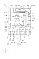
- 2 is a plan view schematically showing the internal structure of the insulation module of FIG. 1.
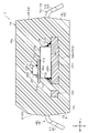
- FIG. 3 is a cross-sectional view of the insulation module of FIG. 2 taken along line 3--3.
- 4 is an enlarged view of a light emitting element and its periphery in the insulation module of FIG. 3.
- FIG. 5 is an enlarged view of the light-emitting element, the light-receiving element, and the periphery thereof in the insulation module of FIG. 6 is a cross-sectional view of the insulation module of FIG. 2 taken along line 6--6.
- FIG. 7 is a cross-sectional view schematically showing the internal structure of part of the light emitting device.
- FIG. 8 is a cross-sectional view schematically showing the internal structure of part of the light receiving element.
- 9 is an enlarged plan view of a part of the sealing resin of the insulation module of FIG. 1.
- FIG. 10 is an enlarged plan view of a part different from FIG. 9 of the sealing resin of the insulation module of FIG. 1.
- FIG. 11 is a circuit diagram schematically showing the electrical configuration of the insulation module of FIG. 1.
- FIG. 12 is a plan view showing an enlarged part of the internal structure of the insulation module of the modification.
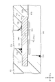
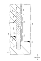
- FIG. 13 is a cross-sectional view of a plate-like member and its surroundings in an insulation module of a modification.
- FIG. 14 is a cross-sectional view of a plate-like member and its periphery in an insulation module of a modification.
- FIG. 15 is a cross-sectional view of a plate-like member and its surroundings in an insulation module of a modification.
- FIG. 16 is a cross-sectional view of a light-receiving element and its surroundings in an insulation module of a modification.
- FIG. 17 is a cross-sectional view schematically showing the internal structure of part of the light receiving element of the insulation module of the modification.
- FIG. 18 is a cross-sectional view schematically showing the internal structure of part of the light receiving element of the insulation module of the modification.
- FIG. 19 is a circuit diagram schematically showing the electrical configuration of the insulation module of the modification.
- FIG. 20 is a circuit diagram schematically showing the electrical configuration of the insulation module of the modification.
- FIG. 1 and 2 show the overall structure of the isolation module 10.
- FIG. FIG. 3 shows the entire cross-sectional structure inside the insulation module 10
- FIG. 7 shows a partial internal structure of the first light emitting element 20P
- FIG. 8 shows a partial internal structure of the first light receiving element 30P.
- 9 and 10 show the appearance of part of the insulation module 10.
- FIG. FIG. 11 shows an example of the circuit configuration of the insulation module 10. As shown in FIG.
- the insulation module 10 is used for a gate driver that applies a drive voltage signal to the gates of switching elements. As shown in FIGS. 1 and 2, the insulation module 10 has a package structure of DIP (Dual In-line Package).
- the insulation module 10 includes a rectangular sealing resin 80 and a plurality of terminals 41 and 51 projecting from the sealing resin 80 .
- the insulation voltage of the insulation module 10 is, for example, 3500 Vrms or more and 7500 Vrms or less. However, the specific numerical value of the dielectric strength voltage of the insulation module 10 is not limited to this and is arbitrary.
- the encapsulating resin 80 is made of an insulating material with light shielding properties.
- An example of an insulating material is epoxy resin.
- the sealing resin 80 is made of black epoxy resin.
- the thickness direction of the sealing resin 80 is defined as the z-direction, and two mutually orthogonal directions among the directions orthogonal to the z-direction are defined as the x-direction and the y-direction, respectively. Note that the z-direction can also be said to be the "height direction of the insulation module".
- the resin main surface 80s and the resin rear surface 80r constitute both end surfaces of the sealing resin 80 in the thickness direction (z direction). Both the resin main surface 80s and the resin rear surface 80r are formed in a rectangular shape when viewed from the z direction.
- the shape of both the resin main surface 80s and the resin rear surface 80r viewed from the z-direction is a rectangular shape with short sides in the x-direction and long sides in the y-direction.
- the first resin side surface 81 and the second resin side surface 82 form both end surfaces in the x direction. Both the first resin side surface 81 and the second resin side surface 82 extend along the y direction when viewed from the z direction.
- a plurality of (four in this embodiment) terminals 41A to 41D are provided on the first resin side surface 81, and a plurality of (four in this embodiment) terminals 51A to 51D are provided on the second resin side surface 82.
- both the first resin side surface 81 provided with the terminals 41A to 41D and the second resin side surface 82 provided with the terminals 51A to 51D correspond to the "terminal surface".
- a plurality of terminals 41A to 41D protrude from the first resin side surface 81.
- a plurality of terminals 51A to 51D protrude from the second resin side surface . Therefore, when viewed from the z direction, it can be said that the plurality of terminals 41A to 41D and the plurality of terminals 51A to 51D are arranged side by side at intervals in the x direction. In other words, the x direction can also be said to be the direction in which the terminals 41A to 41D and the terminals 51A to 51D are arranged.
- the plurality of terminals 51A-51D have the same shape as the plurality of terminals 41A-41D. In this manner, the plurality of terminals 41A to 41D are provided side by side on the first resin side surface 81, and the plurality of terminals 51A to 51D are provided side by side on the second resin side surface .
- the third resin side surface 83 and the fourth resin side surface 84 constitute both end surfaces in the y direction. Both the third resin side surface 83 and the fourth resin side surface 84 are side surfaces on which the plurality of terminals 41A to 41D and 51A to 51D are not provided. Both the third resin side surface 83 and the fourth resin side surface 84 extend along the x direction when viewed from the z direction.
- each of the terminals 41A to 41D and 51A to 51D have the same shape. More specifically, as shown in FIG. 1, each of the terminals 41A to 41D has a first portion extending in the x direction from the first resin side surface 81, a first bent portion bent downward from the first portion, and an x a second portion extending so as to incline downward as it moves away from the sealing resin 80 in the direction; a second bent portion that is bent outward from the second portion; and a third portion extending at an angle. The tilt angle of the third portion with respect to the z-direction is smaller than the tilt angle of the second portion with respect to the z-direction.
- each of the terminals 41A-41D and 51A-51D has a so-called gull-wing type terminal.
- the plurality of terminals 41A to 41D and 51A to 51D constitute external terminals mounted on lands provided on the wiring board (not shown) when the insulation module 10 is mounted on the wiring board, for example.
- the terminals 41A to 41D and 51A to 51D are joined to the lands of the wiring board by a conductive joining material formed of solder, Ag (silver) paste, or the like. Thereby, the insulation module 10 is electrically connected to the wiring board.
- Each resin side surface 81-84 has a first side surface 85 and a second side surface 86.
- the first side surface 85 is continuous with the second side surface 86 .
- the first side surface 85 is arranged closer to the resin main surface 80s than the resin back surface 80r in the z-direction.
- the second side surface 86 is arranged closer to the resin rear surface 80r than the resin main surface 80s in the z-direction.
- the first side surface 85 of the first resin side surface 81 and the first side surface 85 of the second resin side surface 82 are inclined so as to approach each other in the x direction toward the resin main surface 80s.
- the side surface 86 and the second side surface 86 of the second resin side surface 82 are inclined so as to approach each other in the x direction toward the resin back surface 80r.
- a first side surface 85 (not shown) of the third resin side surface 83 and a first side surface 85 of the fourth resin side surface 84 are inclined toward each other in the y direction toward the resin main surface 80s.
- a second side surface 86 (not shown) of 83 and a second side surface 86 of the fourth resin side surface 84 are inclined so as to approach each other in the y direction toward the resin back surface 80r.
- the four terminals 41A to 41D protrude from between the first side surface 85 and the second side surface 86 of the first resin side surface 81 respectively.
- the four terminals 41A-41D are arranged apart from each other in the y direction.
- the four terminals 51A to 51D protrude from between the first side surface 85 and the second side surface 86 of the second resin side surface 82 respectively.
- the four terminals 51A to 51D are arranged apart from each other in the y direction.
- FIG. 2 is a plan view of the insulation module 10 showing the internal structure of the insulation module 10. As shown in FIG. In FIG. 2, the sealing resin 80 is indicated by a chain double-dashed line for convenience.
- the insulation module 10 includes a first light emitting element 20P and a second light emitting element 20Q, a first light receiving element 30P and a second light receiving element 30Q, a first lead frame 40 and a second lead frame 50. and has.
- a first photocoupler is composed of the first light emitting element 20P and the first light receiving element 30P
- a second photocoupler is composed of the second light emitting element 20Q and the second light receiving element 30Q.
- the sealing resin 80 seals at least the light emitting elements 20P and 20Q and the light receiving elements 30P and 30Q.
- the first lead frame 40 is a lead frame electrically connected to the first light receiving element 30P
- the second lead frame 50 is a lead frame electrically connected to the second light receiving element 30Q.
- the first lead frame 40 includes first lead frames 40A to 40D as four first lead frames.
- the first lead frames 40A to 40D are arranged apart from each other in the y direction when viewed from the z direction.
- the first lead frame 40A is arranged closer to the third resin side surface 83 than the first lead frames 40B to 40D.
- the first lead frame 40A includes terminals 41A.
- the terminal 41A is a portion of the first lead frame 40A protruding from the first resin side surface 81 to the outside of the sealing resin 80 .
- Inner leads 42A which are portions of the first lead frame 40A provided in the sealing resin 80, have lead portions 42AA and wire connection portions 42AB.
- the lead portion 42AA is a portion continuous with the terminal 41A and extends in the x direction.
- a wire connecting portion 42AB is provided at the tip of the lead portion 42AA.
- the wire connecting portion 42AB has a portion extending in the y direction toward the fourth resin side surface 84 with respect to the lead portion 42AA. That is, the wire connection portion 42AB has a portion protruding toward the fourth resin side surface 84 with respect to the lead portion 42AA.
- the sealing resin 80 exists on both sides of the wire connecting portion 42AB in the x direction. Therefore, it is possible to prevent the first lead frame 40A from moving in the x direction with respect to the sealing resin 80 by the wire connecting portion 42AB.
- the first lead frame 40B is arranged near the fourth resin side surface 84 with respect to the first lead frame 40A.
- the first lead frame 40B includes terminals 41B. That is, the terminal 41B is a portion of the first lead frame 40B protruding from the first resin side surface 81 to the outside of the sealing resin 80 .
- Inner leads 42B which are portions of the first lead frame 40B provided in the sealing resin 80, have lead portions 42BA and wire connection portions 42BB.
- the lead portion 42BA is a portion continuous with the terminal 41B and extends in the x direction.
- a wire connecting portion 42BB is provided at the tip of the lead portion 42BA.
- the wire connection portion 42BB has a portion extending in the y direction toward the fourth resin side surface 84 with respect to the lead portion 42BA. That is, the wire connection portion 42BB has a portion protruding toward the fourth resin side surface 84 with respect to the lead portion 42BA.
- the length of the wire connection portion 42BB in the y direction is longer than the length of the wire connection portion 42AB in the y direction.
- the sealing resin 80 exists on both sides of the wire connection portion 42BB in the x direction. Therefore, it is possible to suppress the movement of the first lead frame 40B in the x direction with respect to the sealing resin 80 by the wire connection portion 42BB.
- the first lead frame 40C is arranged near the fourth resin side surface 84 with respect to the first lead frame 40B.
- the first lead frame 40C includes terminals 41C. That is, the terminal 41C is a portion of the first lead frame 40C protruding from the first resin side surface 81 to the outside of the sealing resin 80 .
- Inner leads 42C which are portions of the first lead frame 40C provided in the sealing resin 80, have lead portions 42CA and wire connection portions 42CB.
- the lead portion 42CA is a portion continuous with the terminal 41C and extends in the x direction.
- a wire connecting portion 42CB is provided at the tip of the lead portion 42CA.
- the wire connection portion 42CB has portions extending on both sides in the y direction with respect to the lead portion 42CA.
- the wire connection portion 42CB has portions protruding toward both sides in the y direction with respect to the lead portion 42CA.
- the length of the wire connection portion 42CB in the y direction is longer than the length of the wire connection portion 42BB in the y direction.
- the sealing resin 80 exists on both sides of the wire connecting portion 42CB in the x direction. Therefore, it is possible to prevent the first lead frame 40C from moving in the x direction with respect to the sealing resin 80 by the wire connecting portion 42CB.
- the first lead frame 40D is arranged near the fourth resin side surface 84 with respect to the first lead frame 40C.
- the first lead frame 40D includes terminals 41D. That is, the terminal 41D is a portion of the first lead frame 40D protruding from the first resin side surface 81 to the outside of the sealing resin 80. As shown in FIG.
- the inner lead 42D which is the portion of the first lead frame 40D provided in the sealing resin 80, has a lead portion 42DA and a die pad portion 42DB.
- the die pad portion 42DB corresponds to the "die pad”.
- the lead portion 42DA is a portion continuous with the terminal 41D and has a first portion 43D extending in the x direction and a second portion 44D extending in the y direction.
- the first portion 43D is continuous with the terminal 41D.
- the second portion 44D is a portion that connects the first portion 43D and the die pad portion 42DB.
- the second portion 44D is arranged closer to the second resin side surface 82 than the first lead frames 40A to 40C. When viewed in the x direction, the second portion 44D extends to a position overlapping the first lead frame 40C.
- the width of the second portion 44D (the length of the second portion 44D in the y direction) is narrower than the width of the first portion 43D (the length of the first portion 43D in the x direction).
- the die pad portion 42DB is arranged closer to the third resin side surface 83 than the center of the sealing resin 80 in the y direction.
- the die pad portion 42DB is arranged closer to the second resin side surface 82 than the first lead frames 40A to 40C in the x direction.
- the shape of the die pad portion 42DB viewed from the z direction is a rectangular shape with long sides in the x direction and short sides in the y direction.
- the die pad portion 42DB is provided so as to overlap the first lead frames 40A and 40B when viewed in the x direction.
- a protrusion 45D and a suspension lead 46D are provided on the die pad portion 42DB.
- the protrusion 45D extends in the x-direction toward the second resin side surface 82 from a corner near the second resin side surface 82 and the third resin side surface 83 among the four corners of the die pad portion 42DB.
- the width of the projection 45D (the length of the projection 45D in the y direction) is equal to the width of the lead portion 42AA (the length of the lead portion 42AA in the y direction). That is, the width of the projection 45D is wider than the width of the second portion 44D.
- the suspension lead 46D extends in the x-direction toward the first resin side surface 81 from the end closer to the first resin side surface 81 among the x-direction end portions of the die pad portion 42DB.
- the tip of the suspension lead 46 ⁇ /b>D is exposed from the first resin side surface 81 .
- the suspension lead 46D is arranged between the first lead frame 40A and the first lead frame 40B in the y direction. That is, the portion of the suspension lead 46D exposed from the first resin side surface 81 is located between the terminal 41A and the terminal 41B in the y direction.
- the second lead frame 50 includes second lead frames 50A to 50D as four second lead frames.
- the second lead frames 50A to 50D are arranged apart from each other in the y direction when viewed from the z direction.
- the second lead frame 50A is arranged closer to the third resin side surface 83 than the second lead frames 50B to 50D.
- the second lead frame 50A includes terminals 51A.
- the terminal 51A is a portion of the second lead frame 50A protruding outside the sealing resin 80 from the second resin side surface 82 .
- the terminal 51A is arranged at a position overlapping the terminal 41A when viewed in the x direction.
- Inner leads 52A which are portions of the second lead frame 50A provided in the sealing resin 80, have lead portions 52AA and wire connection portions 52AB.
- the lead portion 52AA is a portion continuous with the terminal 51A and extends in the x direction.
- a wire connecting portion 52AB is provided at the tip of the lead portion 52AA.
- the wire connection portion 52AB has a portion extending in the y direction toward the fourth resin side surface 84 with respect to the lead portion 52AA. That is, the wire connecting portion 52AB has a portion protruding toward the fourth resin side surface 84 with respect to the lead portion 52AA.
- the y-direction length of the wire connection portion 52AB is longer than the y-direction length of the wire connection portion 42AB of the first lead frame 40A.
- the y-direction length of the wire connection portion 52AB is longer than the y-direction length of the wire connection portion 42CB of the first lead frame 40C.
- the lead portion 52AA and the wire connection portion 52AB are arranged at positions facing the protrusion 45D of the first lead frame 40D in the x direction.
- the wire connecting portion 52AB is arranged closer to the second resin side surface 82 than the projection 45D.
- the sealing resin 80 exists on both sides of the wire connecting portion 52AB in the x direction. Therefore, it is possible to suppress the movement of the second lead frame 50A in the x-direction with respect to the sealing resin 80 by the wire connecting portion 52AB.
- the second lead frame 50B is arranged closer to the fourth resin side surface 84 than the second lead frame 50A.
- the second lead frame 50B includes terminals 51B. That is, the terminal 51B is a portion of the second lead frame 50B protruding from the second resin side surface 82 to the outside of the sealing resin 80 . In this embodiment, the terminal 51B is arranged at a position overlapping the terminal 41B when viewed in the x direction.
- Inner leads 52B which are portions of the second lead frame 50B provided in the sealing resin 80, have lead portions 52BA and wire connection portions 52BB.
- the lead portion 52BA is a portion continuous with the terminal 51B and extends in the x direction.
- a wire connecting portion 52BB is provided at the tip of the lead portion 52BA.
- the wire connection portion 52BB has a portion extending in the y direction toward the fourth resin side surface 84 with respect to the lead portion 52BA. That is, the wire connection portion 52BB has a portion protruding toward the fourth resin side surface 84 with respect to the lead portion 52BA.
- the y-direction length of the wire connection portion 52BB is shorter than the y-direction length of the wire connection portion 52AB of the second lead frame 50A.
- the lead portion 52BA and the wire connection portion 52BB are arranged at positions facing the die pad portion 42DB of the first lead frame 40D in the x direction.
- the wire connection portion 52BB is arranged closer to the second resin side surface 82 than the projection 45D.
- the sealing resin 80 exists on both sides of the wire connection portion 52BB in the x direction. Therefore, it is possible to suppress the movement of the second lead frame 50B in the x-direction with respect to the sealing resin 80 by the wire connection portion 52BB.
- the second lead frame 50C is arranged closer to the fourth resin side surface 84 than the second lead frame 50B.
- the second lead frame 50C includes terminals 51C.
- the terminal 51C is a portion of the second lead frame 50C protruding outside the sealing resin 80 from the second resin side surface 82 .
- the terminal 51C is arranged at a position overlapping the terminal 41C when viewed in the x direction.
- Inner leads 52C which are portions of the second lead frame 50C provided in the sealing resin 80, have lead portions 52CA and wire connection portions 52CB.
- the lead portion 52CA is a portion continuous with the terminal 51C and extends in the x direction.
- a wire connecting portion 52CB is provided at the tip of the lead portion 52CA.
- the wire connection portion 52CB has a portion extending in the y direction toward the fourth resin side surface 84 with respect to the lead portion 52CA. That is, the wire connection portion 52CB has a portion protruding toward the fourth resin side surface 84 with respect to the lead portion 52CA.
- the y-direction length of the wire connection portion 52CB is shorter than the y-direction length of the wire connection portion 52BB of the second lead frame 50B.
- the lead portion 52CA and the wire connection portion 52CB are arranged closer to the side surface of the fourth resin than the die pad portion 42DB of the first lead frame 40D in the x direction.
- the wire connection portion 52CB is arranged closer to the second resin side surface 82 than the die pad portion 42DB.
- the sealing resin 80 exists on both sides of the wire connection portion 52CB in the x direction. Therefore, it is possible to suppress the movement of the second lead frame 50C in the x-direction with respect to the sealing resin 80 by the wire connection portion 52CB.
- the second lead frame 50D is arranged closer to the fourth resin side surface 84 than the second lead frame 50C.
- the second lead frame 50D includes terminals 51D. That is, the terminal 51D is a portion of the second lead frame 50D protruding from the second resin side surface 82 to the outside of the sealing resin 80 . In this embodiment, the terminal 51D is arranged at a position overlapping the terminal 41D when viewed in the x direction.
- An inner lead 52D which is a portion of the second lead frame 50D provided in the sealing resin 80, has a lead portion 52DA, a die pad portion 52DB, and a wire connection portion 52DC.
- the lead portion 52DA is a portion continuous with the terminal 51D and extends in the x direction.
- the length of the lead portion 52DA in the x direction is longer than the length of the lead portions 52AA to 52CA in the x direction.
- the lead portion 52DA is connected to the die pad portion 52DB.
- the die pad portion 52DB is arranged closer to the fourth resin side surface 84 than the center of the sealing resin 80 in the y direction. It can also be said that the die pad portion 52DB is arranged closer to the fourth resin side surface 84 than the die pad portion 42DB of the first lead frame 40D.
- the die pad portion 52DB is arranged side by side with the die pad portion 42DB in the y direction.
- the die pad portion 52DB is arranged closer to the first resin side surface 81 than the second lead frames 50A to 50C in the x direction.
- the shape of the die pad portion 52DB viewed from the z direction is a rectangular shape with short sides in the x direction and long sides in the y direction.
- the die pad portion 52DB is provided so as to overlap the second lead frame 50C when viewed in the x direction.
- a wire connection portion 52DC is provided at a corner near the third resin side surface 83 and the second resin side surface 82 among the four corners of the die pad portion 52DB.
- the wire connection portion 52DC extends in the y-direction from the die pad portion 52DB toward the third resin side surface 83.
- the wire connection portion 52DC is arranged closer to the second resin side surface 82 than the die pad portion 42DB of the first lead frame 40D, and is arranged at a position overlapping the die pad portion 42DB when viewed in the x direction.
- the wire connection portion 52DC is arranged closer to the first resin side surface 81 than the second lead frames 50A and 50B, and is arranged at a position overlapping the second lead frames 50A and 50B when viewed from the x direction. That is, the wire connection portion 52DC is arranged between the die pad portion 42DB and the second lead frames 50A and 50B in the x direction.
- a wire connection portion 53D is provided in a portion of the lead portion 52DA near the die pad portion 52DB.
- the wire connecting portion 53D is a portion extending in the y-direction from the lead portion 52DA toward the third resin side surface 83. As shown in FIG.
- the wire connection portion 53D is arranged at a position aligned with the wire connection portion 52CB of the second lead frame 50C in the x direction.
- a through hole 54D is provided in a portion of the die pad portion 52DB near the fourth resin side surface 84 .
- the through hole 54D is provided at a position overlapping the lead portion 52DA when viewed from the x direction.
- a sealing resin 80 is filled in the through hole 54D. The sealing resin 80 in the through hole 54D can prevent the second lead frame 50D from moving with respect to the sealing resin 80 in the direction perpendicular to the z direction.
- the first light receiving element 30P is mounted on the die pad portion 42DB of the first lead frame 40D
- the second light receiving element 30Q is mounted on the die pad portion 52DB of the second lead frame 50D
- the first light emitting element 20P is mounted on the first light receiving element 30P
- the second light emitting element 20Q is mounted on the second light receiving element 30Q.
- the first light receiving element 30P and the second light receiving element 30Q are light receiving elements having the same shape and size. Light emitting elements having the same shape and size are used for the first light emitting element 20P and the second light emitting element 20Q.
- the die pad portion 42DB corresponds to the "first die pad”
- the die pad portion 52DB corresponds to the "second die pad”.
- the first light receiving element 30P is arranged biased toward the second resin side surface 82 with respect to the die pad portion 42DB. That is, the center of the first light receiving element 30P in the x direction is positioned closer to the second resin side surface 82 than the center of the die pad portion 42DB in the x direction. In this embodiment, the first light receiving element 30P is arranged closer to the second resin side surface 82 than the lead portion 42DA in the x direction.
- the first light receiving element 30P is joined to the die pad portion 42DB with a conductive joining material 100P (see FIG. 6) such as solder or Ag (silver) paste.
- the first light receiving element 30P is joined to the die pad portion 42DB by being die-bonded to the die pad portion 42DB.
- the shape of the first light receiving element 30P viewed from the z direction is a rectangular shape with short sides in the x direction and long sides in the y direction.
- the conductive bonding material 100P corresponds to the "light receiving bonding material”.
- the second light receiving element 30Q is arranged biased toward the first resin side surface 81 with respect to the die pad portion 52DB. That is, the center of the second light receiving element 30Q in the x direction is positioned closer to the first resin side surface 81 than the center of the die pad portion 52DB in the x direction. In this embodiment, the second light receiving element 30Q is arranged closer to the first resin side surface 81 than the wire connecting portion 52DC in the x direction.
- the second light receiving element 30Q is bonded to the die pad portion 52DB with a conductive bonding material 100Q (see FIG. 6) such as solder or Ag paste.
- the second light receiving element 30Q is joined to the die pad portion 52DB by being die-bonded to the die pad portion 52DB.
- the conductive bonding material 100Q corresponds to the "light receiving bonding material".
- the first light receiving element 30P and the second light receiving element 30Q are arranged side by side in the y direction. More specifically, the first light-receiving element 30P and the second light-receiving element 30Q are arranged to overlap each other when viewed in the y direction. On the other hand, the first light-receiving element 30P and the second light-receiving element 30Q are arranged to be offset from each other in the x direction. The first light receiving element 30P is arranged so as to be shifted toward the first resin side surface 81 with respect to the second light receiving element 30Q in the x direction.
- the end portion closer to the first resin side surface 81 is arranged closer to the first resin side surface 81 than the second light receiving element 30Q when viewed from the y direction.
- the second light receiving element 30Q is arranged shifted toward the second resin side surface 82 with respect to the first light receiving element 30P in the x direction. That is, of the x-direction end portions of the second light receiving element 30Q, the end portion closer to the second resin side surface 82 is arranged closer to the second resin side surface 82 than the first light receiving element 30P when viewed from the y direction. ing.
- the first light emitting element 20P is arranged at a position overlapping the first light receiving element 30P when viewed from the z direction. More specifically, the first light emitting element 20P is arranged closer to the second resin side surface 82 than the center of the first light receiving element 30P in the x direction when viewed in the z direction. Among both edges of the first light emitting element 20P in the x direction, the edge closer to the second resin side surface 82 is the edge closer to the second resin side surface 82 than both edges of the first light receiving element 30P in the x direction. is arranged closer to the first resin side surface 81 than the first resin side surface 81 .
- the edge closer to the first resin side surface 81 is arranged closer to the second resin side surface 82 than the center of the first light receiving element 30P in the x direction.
- the first light emitting element 20P is arranged closer to the third resin side surface 83 than the center of the first light receiving element 30P in the y direction when viewed from the z direction. More specifically, when viewed from the z direction, the first light emitting element 20P is arranged at a position overlapping the first virtual line VL1 extending along the x direction at the center of the first light receiving element 30P in the y direction.
- the y-direction center of the first light emitting element 20P is arranged closer to the third resin side surface 83 than the first virtual line VL1.
- the shape of the first light emitting element 20P viewed from the z direction is a rectangular shape with short sides in the x direction and long sides in the y direction.
- the area of the first light emitting element 20P is smaller than half the area of the first light receiving element 30P.
- the area of the first light emitting element 20P is larger than 1/10 of the area of the first light receiving element 30P and smaller than 1/2 of the area of the first light receiving element 30P.
- the area of the first light emitting element 20P is about 1/9 of the area of the first light receiving element 30P when viewed from the z direction.
- the first light emitting element 20P has an element main surface 20Ps and an element rear surface 20Pr facing opposite sides in the thickness direction of the first light emitting element 20P.
- the element main surface 20Ps faces the same side as the pad main surface 42Ds of the die pad portion 42DB, and the element rear surface 20Pr faces the same side as the pad rear surface 42Dr.
- the element rear surface 20Pr constitutes the light emitting surface of the first light emitting element 20P. Therefore, the element main surface 20Ps corresponds to "the back surface facing away from the light emitting surface".
- the second light emitting element 20Q is arranged at a position overlapping the second light receiving element 30Q when viewed from the z direction. More specifically, the second light emitting element 20Q is arranged closer to the first resin side surface 81 than the center of the second light receiving element 30Q in the x direction when viewed in the z direction. Of the x-direction edges of the second light emitting element 20Q, the edge closer to the first resin side surface 81 is the edge of the x-direction edge of the second light receiving element 30Q that is closer to the first resin side surface 81. It is arranged closer to the second resin side surface 82 than the second resin side surface 82 .
- the edge closer to the second resin side surface 82 is arranged closer to the first resin side surface 81 than the center of the second light receiving element 30Q in the x direction.
- the second light emitting element 20Q is arranged closer to the fourth resin side surface 84 than the center of the second light receiving element 30Q in the y direction when viewed from the z direction. More specifically, when viewed from the z direction, the second light emitting element 20Q is arranged at a position overlapping the second virtual line VL2 extending along the x direction at the center of the second light receiving element 30Q in the y direction.
- the center of the second light emitting element 20Q in the y direction is arranged closer to the fourth resin side surface 84 than the second virtual line VL2. Note that the relationship between the area of the second light emitting element 20Q and the area of the second light receiving element 30Q when viewed from the z-direction is the same as that of the first light emitting element 20P and the first light receiving element 30P, so detailed description is omitted. .
- the first light emitting element 20P has an element main surface 20Qs and an element rear surface 20Qr facing opposite sides in the thickness direction of the second light emitting element 20Q.
- the element main surface 20Qs faces the same side as the pad main surface 52Ds of the die pad portion 52DB, and the element rear surface 20Qr faces the same side as the pad rear surface 52Dr.
- the element rear surface 20Qr constitutes the light emitting surface of the second light emitting element 20Q. Therefore, the element main surface 20Qs corresponds to "the back surface facing away from the light emitting surface".
- the first light emitting element 20P and the second light emitting element 20Q are arranged apart from each other in the y direction.
- the first light emitting element 20P is arranged closer to the second resin side surface 82 than the second light emitting element 20Q.
- the second light emitting element 20Q is arranged closer to the first resin side surface 81 than the first light emitting element 20P.
- the first light emitting element 20P and the second light emitting element 20Q are arranged at positions that do not overlap each other.
- the first light emitting element 20P emits light of a first wavelength.
- An example of light of the first wavelength is light of wavelengths including infrared.
- the second light emitting element 20Q emits light of a second wavelength different from the first wavelength.
- An example of light of the second wavelength is light of wavelengths including red. Both the first light emitting element 20P and the second light emitting element 20Q emit light downward.
- the first light receiving element 30P is configured to be able to receive light (light of the first wavelength) from the first light emitting element 20P.
- the first light receiving element 30P includes a first semiconductor region that receives light from the first light emitting element 20P and a second semiconductor region that generates a signal based on the received light.
- a photoelectric conversion element is provided in the first semiconductor region. Photodiodes, for example, are used as photoelectric conversion elements.
- the second semiconductor region is formed by, for example, LSI (Large Scale Integration). That is, the first light receiving element 30P of the present embodiment is an element in which the function of receiving light from the first light emitting element 20P and the function of generating a signal from the received light are integrated.
- the first semiconductor region and the second semiconductor region are formed side by side in the x-direction.
- the first semiconductor region is formed in a portion of the first light receiving element 30P which overlaps with the first light emitting element 20P when viewed from the z direction.
- the first light emitting element 20P is arranged biased toward the photoelectric conversion element with respect to the first light receiving element 30P.
- the second semiconductor region is formed in a portion of the first light receiving element 30P near the second resin side surface 82 when viewed in the z direction.
- the area of the first semiconductor region viewed in the z-direction is smaller than the area of the second semiconductor region viewed in the z-direction.
- the x-direction dimension of the first semiconductor region is smaller than the x-direction dimension of the second semiconductor region.
- the first semiconductor region of the first light receiving element 30P forms a light receiving surface 33P. That is, the first light emitting element 20P is arranged at a position overlapping the light receiving surface 33P of the first light receiving element 30P when viewed from the z direction. Therefore, the light receiving surface 33P of the first light receiving element 30P faces the element rear surface 20Pr (light emitting surface) of the first light emitting element 20P.
- the second light receiving element 30Q is configured to receive light (light of the second wavelength) from the second light emitting element 20Q. Since the second light receiving element 30Q has the same configuration as the first light receiving element 30P, detailed description thereof will be omitted.
- the second light receiving element 30Q similarly has a light receiving surface 33Q as a first semiconductor region.
- the second light-emitting element 20Q is arranged at a position overlapping the light-receiving surface 33Q of the second light-receiving element 30Q when viewed from the z-direction. Therefore, the light receiving surface 33Q of the second light receiving element 30Q faces the element rear surface 20Qr (light emitting surface) of the second light emitting element 20Q. Also, the second light emitting element 20Q is arranged biased toward the photoelectric conversion element with respect to the second light receiving element 30Q.
- the first light receiving element 30P has an element main surface 30Ps and an element back surface 30Pr facing opposite sides in the thickness direction of the first light receiving element 30P.
- the element main surface 30Ps faces the same side as the pad main surface 42Ds of the die pad portion 42DB, and the element rear surface 30Pr faces the same side as the pad rear surface 42Dr.
- the element main surface 30Ps includes a light receiving surface 33P. Therefore, in this embodiment, the back surface 30Pr of the element constitutes "the back surface facing away from the light receiving surface". Further, the element main surface 30Ps faces the same side as the resin main surface 80s (see FIG. 3) of the sealing resin 80, and the element rear surface 30Pr faces the same side as the resin rear surface 80r (see FIG.
- the sealing resin 80 there is That is, the light receiving surface 33P faces the same side as the resin main surface 80s, and the element rear surface 20Pr of the first light emitting element 20P, which is the light emitting surface facing the light receiving surface 33P, faces the same side as the resin rear surface 80r.
- the second light receiving element 30Q has an element main surface 30Qs and an element back surface 30Qr facing opposite sides in the thickness direction of the second light receiving element 30Q.
- the element main surface 30Qs faces the same side as the pad main surface 52Ds of the die pad portion 52DB, and the element rear surface 30Qr faces the same side as the pad rear surface 52Dr.
- the element main surface 30Qs includes a light receiving surface 33Q. Therefore, in this embodiment, the back surface 30Qr of the element constitutes "the back surface facing away from the light receiving surface".
- the element main surface 30Qs faces the same side as the resin main surface 80s of the sealing resin 80, and the element rear surface 30Qr faces the same side as the resin rear surface 80r of the sealing resin 80.
- the light receiving surface 33Q faces the same side as the resin main surface 80s
- the element rear surface 20Qr of the second light emitting element 20Q which is the light emitting surface facing the light receiving surface 33Q, faces the same side as the resin rear surface 80r.
- the light of the first wavelength from the first light emitting element 20P and the light of the second wavelength from the second light emitting element 20Q can be changed arbitrarily.
- both the first light emitting element 20P and the second light emitting element 20Q may be configured to emit visible light.
- the first light emitting element 20P may be configured to emit light of wavelengths including blue
- the second light emitting element 20Q may be configured to emit light of wavelengths including red.
- the light of the first wavelength from the first light emitting element 20P and the light of the second wavelength from the second light emitting element 20Q are lights having different wavelengths, but the present invention is not limited to this.
- the first light emitting element 20P and the second light emitting element 20Q may be configured to emit light of the same wavelength. In one example, both the first light emitting element 20P and the second light emitting element 20Q are configured to emit light including red wavelengths. In another example, both the first light emitting element 20P and the second light emitting element 20Q are configured to emit light of wavelengths including infrared rays.
- the configuration of the die pad portion 42DB, the first light emitting element 20P, and the first light receiving element 30P, and the layout of the die pad portion 42DB, the first light receiving element 30P, and the first light emitting element 20P are the second light emitting element 20Q, Since it is similar to the second light receiving element 30Q and the die pad portion 52DB, detailed description thereof will be omitted.
- the internal structures of the second light emitting element 20Q and the second light receiving element 30Q are omitted.
- the die pad portion 52DB is arranged closer to the resin back surface 80r than the position where the terminal 51D projects from the second resin side surface 82 in the z direction. Therefore, the lead portion 52DA has a portion that is bent toward the resin back surface 80r toward the die pad portion 52DB.
- the die pad portion 52DB has a pad main surface 52Ds and a pad rear surface 52Dr facing opposite sides in the thickness direction.
- the pad main surface 52Ds is a surface forming a mounting surface on which the second light receiving element 30Q is mounted, and faces the same side as the resin main surface 80s.
- the pad back surface 52Dr faces the same side as the resin back surface 80r.
- the pad back surface 52Dr is arranged apart from the resin back surface 80r in the z direction. That is, the pad rear surface 52Dr is not exposed from the resin rear surface 80r.
- the die pad portion 52DB has a main metal layer 55D and a plated layer 56D formed on the outer surface of the main metal layer 55D.
- the main metal layer 55D is made of a metal material containing Cu, for example.
- the plated layer 56D is made of a material containing Ni (nickel), Cr (chromium), or the like. As shown in FIG. 5, the plating layer 56D is sufficiently thin compared to the main metal layer 55D.
- the conductive bonding material 100Q that bonds the second light receiving element 30Q and the die pad portion 52DB is a first bonding region 101Q interposed between the element rear surface 30Qr of the second light receiving element 30Q and the pad main surface 52Ds of the die pad portion 52DB. , and a second junction region 102Q that protrudes from the second light receiving element 30Q when viewed in the z direction and is joined to the outer surface of the second light receiving element 30Q.
- the second junction region 102Q is provided so that the thickness of the second junction region 102Q becomes thinner as the distance from the outer surface of the second light receiving element 30Q increases.
- the second junction region 102Q is formed over the entire circumference of the second light receiving element 30Q when viewed from the z direction.
- the height HT of the portion of the second junction region 102Q in contact with the outer surface of the second light receiving element 30Q is higher than 1/2 or less of the height HRQ of the second light receiving element 30Q.
- the height HT is about 2/3 of the height HRQ.
- the height HT is defined by the height from the pad main surface 52Ds of the die pad portion 52DB of the portion of the second junction region 102Q in contact with the outer side surface of the second light receiving element 30Q. That is, it can be said that the height HT is the thickness of the portion of the second junction region 102Q that is in contact with the outer side surface of the second light receiving element 30Q.
- the height HRQ is defined by the distance in the z direction between the pad main surface 52Ds of the die pad portion 52DB and the element main surface 30Qs of the second light receiving element 30Q.
- the conductive bonding material 100P that bonds the first light receiving element 30P and the die pad portion 42DB has a first bonding region 101P and a second bonding region 102P (see FIG. 6) like the conductive bonding material 100Q. reference).
- the first bonding region 101P is interposed between the element rear surface 30Pr of the first light receiving element 30P and the pad main surface 42Ds of the die pad portion 42DB.
- the second bonding region 102P is a region protruding from the first light receiving element 30P when viewed in the z direction and is bonded to the outer side surface of the first light receiving element 30P. Note that the first bonding region 101P and the second bonding region 102P are the same as the conductive bonding material 100Q, so detailed description thereof will be omitted.
- the insulation module 10 includes a first plate member 70P laminated on the first light receiving element 30P, a second plate member 70Q laminated on the second light receiving element 30Q, and a first plate member 70Q.
- both the first plate-like member 70P and the second plate-like member 70Q correspond to the "insulating member". Both the first plate member 70P and the second plate member 70Q have translucency.
- the first light emitting element 20P is arranged on the first plate member 70P, and the second light emitting element 20Q is arranged on the second plate member 70Q. That is, the first plate member 70P and the first transparent resin 60P are interposed between the first light emitting element 20P and the first light receiving element 30P in the z direction, and the second light emitting element 20Q and the second light receiving element 30Q are interposed. A second plate member 70Q and a second transparent resin 60Q are interposed between them in the z direction.
- the first transparent resin 60P is formed on the element main surface 30Ps of the first light receiving element 30P. At least part of the first transparent resin 60P is provided on the light receiving surface 33P. In this embodiment, the first transparent resin 60P is formed, for example, over the entire element main surface 30Ps.
- the first transparent resin 60P is a bonding material that bonds the first plate member 70P to the element main surface 30Ps of the first light receiving element 30P.
- the second transparent resin 60Q is formed on the element main surface 30Qs of the second light receiving element 30Q. At least part of the second transparent resin 60Q is provided on the light receiving surface 33Q. In this embodiment, the second transparent resin 60Q is formed, for example, over the entire element main surface 30Qs.
- the second transparent resin 60Q is a bonding material that bonds the second plate member 70Q to the element main surface 30Qs of the second light receiving element 30Q.
- the transparent resins 60P and 60Q insulating materials such as transparent epoxy resin, acrylic resin, and silicone resin are used.
- the first transparent resin 60P is made of an insulating resin through which light (light of the first wavelength) from the first light emitting element 20P can pass.
- the first transparent resin 60P is made of an insulating resin that blocks (does not transmit) the light from the second light emitting element 20Q.
- the second transparent resin 60Q is made of an insulating resin through which light (light of the second wavelength) from the second light emitting element 20Q can pass.
- the second transparent resin 60Q is made of an insulating resin that blocks (does not transmit) the light from the first light emitting element 20P.
- Each transparent resin 60P, 60Q is formed by potting, for example.
- the first plate-like member 70P has a main surface 70Ps and a back surface 70Pr facing opposite sides in the thickness direction.
- the main surface 70Ps faces the same side as the element main surface 30Ps of the first light receiving element 30P
- the rear surface 70Pr faces the same side as the element rear surface 30Pr of the first light receiving element 30P.
- the first plate-like member 70P is in contact with the first transparent resin 60P on the rear surface 70Pr.
- the main surface 70Ps of the first plate member 70P corresponds to the "first surface”
- the rear surface 70Pr corresponds to the "second surface”.
- the first plate member 70P is arranged so as to overlap the first semiconductor region of the first light receiving element 30P.
- the first plate member 70P covers the light receiving surface 33P of the first light receiving element 30P. It can be said that the first plate member 70P is laminated at least on the light receiving surface 33P (see FIG. 2) of the first light receiving element 30P. Therefore, it can be said that the back surface 70Pr of the first plate member 70P faces the light receiving surface 33P.
- the first plate member 70P is arranged to be biased in the x direction with respect to the first light receiving element 30P. More specifically, the first plate-like member 70P is arranged biased toward the second resin side surface 82 with respect to the first light receiving element 30P. The first plate member 70P is arranged closer to the second resin side surface 82 than the wires WB1 to WB4. In one example, the y-direction length of the first plate member 70P is longer than the y-direction length of the first light receiving element 30P.
- the thickness T1 of the second plate member 70Q is thicker than the thickness T2 of the second transparent resin 60Q.
- the thickness T2 of the second transparent resin 60Q is thinner than the thickness T1 of the second plate member 70Q.
- the thickness T1 of the second plate member 70Q is, for example, two to five times the thickness T2 of the second transparent resin 60Q. In this embodiment, the thickness T1 of the second plate member 70Q is approximately four times the thickness T2 of the second transparent resin 60Q.
- the relationship between the thickness of the first plate member 70P and the thickness of the first transparent resin 60P is the same as the relationship between the thickness T1 of the second plate member 70Q and the thickness T2 of the second transparent resin 60Q. .
- the first plate member 70P can be divided into a first extending portion 71P, a second extending portion 72P, and an intermediate portion 73P in the x direction.
- the intermediate portion 73P is provided between the first extension portion 71P and the second extension portion 72P in the x direction, and connects the first extension portion 71P and the second extension portion 72P.
- the first extending portion 71P is a portion protruding toward the first resin side surface 81 with respect to the first light emitting element 20P when viewed in the z direction.
- the second extending portion 72P is a portion protruding toward the second resin side surface 82 with respect to the first light emitting element 20P when viewed in the z direction.
- the second extending portion 72P is a portion protruding from the first light emitting element 20P toward the second semiconductor region of the first light receiving element 30P when viewed in the z direction.
- the second extending portion 72P partially covers the second semiconductor region of the first light receiving element 30P.
- the intermediate portion 73P is a portion that overlaps the first light emitting element 20P when viewed from the z direction. That is, it can be said that the intermediate portion 73P is a portion corresponding to the first light emitting element 20P in the x direction.
- Both the first extending portion 71P and the intermediate portion 73P cover the first semiconductor region (light receiving surface 33P) of the first light receiving element 30P.
- the first extending portion 71P has a portion that protrudes closer to the second resin side surface 82 than the first light receiving element 30P.
- the first extending portion 71P does not protrude from the die pad portion 42DB in the x direction. That is, of the x-direction side surfaces of the first extending portion 71P, the side surface closer to the second resin side surface 82 is the second resin side surface 82 of the x-direction side surfaces of the die pad portion 42DB when viewed from the z direction. is located closer to the first resin side surface 81 than the side surface closer to the .
- the x-direction length of the first extension portion 71P is longer than the x-direction length of the second extension portion 72P.
- the length of the first extending portion 71P in the x direction can be arbitrarily changed.
- the first extending portion 71P may be provided so as to protrude closer to the second resin side surface 82 than the die pad portion 42DB when viewed in the z direction.
- the length in the x direction of the first extending portion 71P may be equal to the length in the x direction of the second extending portion 72P.
- the length of the first extending portion 71P in the x direction may be shorter than the length of the second extending portion 72P in the x direction.
- the second plate member 70Q has a main surface 70Qs and a back surface 70Qr facing opposite sides in the thickness direction.
- the main surface 70Qs faces the same side as the element main surface 30Qs of the second light receiving element 30Q
- the rear surface 70Qr faces the same side as the element rear surface 30Qr of the second light receiving element 30Q.
- the second plate-shaped member 70Q is in contact with the second transparent resin 60Q at the rear surface 70Qr.
- the main surface 70Qs of the second plate member 70Q corresponds to the "first surface”
- the back surface 70Qr corresponds to the "second surface”.
- the second plate member 70Q is arranged so as to overlap the first semiconductor region of the second light receiving element 30Q.
- the second plate member 70Q covers the light receiving surface 33Q of the second light receiving element 30Q. It can be said that the second plate member 70Q is laminated at least on the light receiving surface 33Q (see FIG. 2) of the second light receiving element 30Q. Therefore, it can be said that the back surface 70Qr of the second plate member 70Q faces the light receiving surface 33Q.
- the second plate-shaped member 70Q is arranged to be biased in the x direction with respect to the second light receiving element 30Q. More specifically, the second plate-shaped member 70Q is arranged biased toward the first resin side surface 81 with respect to the second light receiving element 30Q. The second plate member 70Q is arranged closer to the first resin side surface 81 than the wires WC1 to WC3.
- the second plate member 70Q can be divided into a first extending portion 71Q, a second extending portion 72Q, and an intermediate portion 73Q in the x direction.
- the intermediate portion 73Q is provided between the first extension portion 71Q and the second extension portion 72Q in the x direction, and connects the first extension portion 71Q and the second extension portion 72Q.
- the first extending portion 71Q is a portion protruding toward the first resin side surface 81 with respect to the second light emitting element 20Q when viewed in the z direction.
- the second extending portion 72Q is a portion protruding toward the second resin side surface 82 with respect to the second light emitting element 20Q when viewed in the z direction.
- the second extending portion 72Q is a portion protruding from the second light emitting element 20Q toward the second semiconductor region of the second light receiving element 30Q when viewed in the z direction.
- the second extending portion 72Q partially covers the second semiconductor region of the second light receiving element 30Q.
- the intermediate portion 73Q is a portion that overlaps with the second light emitting element 20Q when viewed from the z direction. That is, it can be said that the intermediate portion 73Q is a portion corresponding to the second light emitting element 20Q in the x direction.
- Both the first extending portion 71Q and the intermediate portion 73Q cover the first semiconductor region (light receiving surface 33Q) of the second light receiving element 30Q.
- the first extending portion 71Q has a portion that protrudes closer to the first resin side surface 81 than the second light receiving element 30Q.
- the first extending portion 71Q does not protrude from the die pad portion 52DB in the x direction. That is, of the x-direction side surfaces of the first extending portion 71Q, the side surface closer to the first resin side surface 81 is the first resin side surface 81 of the x-direction side surfaces of the die pad portion 52DB when viewed from the z direction. is positioned closer to the second resin side surface 82 than the side surface closer to the .
- the length in the x direction of the first extension portion 71Q is longer than the length in the x direction of the second extension portion 72Q.
- the length of the first extending portion 71Q in the x direction can be changed arbitrarily.
- the first extending portion 71Q may be provided so as to protrude closer to the first resin side surface 81 than the die pad portion 52DB when viewed in the z direction.
- the length in the x direction of the first extending portion 71Q may be equal to the length in the x direction of the second extending portion 72Q.
- the x-direction length of the first extension portion 71Q may be shorter than the x-direction length of the second extension portion 72Q.
- the light transmittance of the first plate member 70P is lower than the light transmittance of the first transparent resin 60P.
- the first plate member 70P is configured such that its light transmittance is lower than that of the first transparent resin 60P.
- the first plate-like member 70P is made of a material whose light transmittance is lower than that of the first transparent resin 60P. The same applies to the relationship between the second plate member 70Q and the second transparent resin 60Q.
- the light transmittance of the first plate member 70P can be changed arbitrarily.
- the light transmittance of the first plate member 70P may be equal to the light transmittance of the first transparent resin 60P, or may be higher than the light transmittance of the first transparent resin 60P. That is, the light transmittance of the first plate member 70P may be equal to or higher than the light transmittance of the first transparent resin 60P. In other words, the light transmittance of the first transparent resin 60P may be equal to or less than the light transmittance of the first plate member 70P.
- the relationship between the second plate member 70Q and the second transparent resin 60Q may be similarly changed.
- the thickness of the first plate member 70P, the thickness T1 of the second plate member 70Q, the thickness of the first transparent resin 60P, and the thickness T2 of the second transparent resin 60Q can be changed arbitrarily.
- the thickness of the first plate member 70P may be equal to the thickness of the first transparent resin 60P.
- the thickness of the first plate member 70P may be thinner than the thickness of the first transparent resin 60P.
- the thickness of the first transparent resin 60P may be thicker than the thickness of the first plate member 70P. That is, the thickness of the first transparent resin 60P may be equal to or greater than the thickness of the first plate member 70P.
- the thickness T1 of the second plate member 70Q may be equal to the thickness T2 of the second transparent resin 60Q. In another example, the thickness T1 of the second plate member 70Q may be thinner than the thickness T2 of the second transparent resin 60Q. In other words, the thickness T2 of the second transparent resin 60Q may be thicker than the thickness T1 of the second plate member 70Q. That is, the thickness T2 of the second transparent resin 60Q may be equal to or greater than the thickness T1 of the second plate member 70Q.
- the first plate member 70P is made of an insulating resin through which the light (light of the first wavelength) from the first light emitting element 20P can pass.
- the first plate member 70P may be made of an insulating resin that blocks (does not transmit) the light from the second light emitting element 20Q.
- the second plate member 70Q is made of an insulating resin through which light (light of the second wavelength) from the second light emitting element 20Q can pass.
- the second plate member 70Q may be made of an insulating resin that blocks (does not transmit) the light from the first light emitting element 20P.
- each of the transparent resins 60P and 60Q may be made of a resin material that can transmit both the light of the first wavelength and the light of the second wavelength.
- the first light emitting element 20P is arranged on the main surface 70Ps of the first plate member 70P. More specifically, the element rear surface 20Pr of the first light emitting element 20P is in contact with the main surface 70Ps of the first plate member 70P.
- a first transparent resin 60P is formed on the first light receiving element 30P, and a first plate member 70P is arranged on the first transparent resin 60P. In this manner, the first plate member 70P is laminated on the first light receiving element 30P via the first transparent resin 60P, and the first light emitting element 20P is laminated on the first plate member 70P. It can also be said that one light emitting element 20P is stacked on the first light receiving element 30P.
- the first light emitting element 20P is joined to the first plate member 70P by, for example, an insulating joining material 90P.
- the insulating bonding material 90P is applied so that the first light emitting element 20P and the main surface 70Ps of the first plate member 70P are in contact with each other while the first light emitting element 20P is arranged on the main surface 70Ps of the first plate member 70P.
- the first light emitting element 20P is joined to the first plate member 70P. Therefore, the insulating bonding material 90P is not interposed between the element rear surface 20Pr of the first light emitting element 20P and the main surface 70Ps of the first plate member 70P.
- the insulating bonding material 90P corresponds to the "light-emitting bonding material".
- the second light emitting element 20Q is arranged on the main surface 70Qs of the second plate member 70Q. More specifically, the element rear surface 20Qr of the second light emitting element 20Q is in contact with the main surface 70Qs of the second plate member 70Q. In this manner, the second plate member 70Q is stacked on the second light receiving element 30Q, and the second light emitting device 20Q is stacked on the second plate member 70Q. It can also be said that it is stacked on the element 30Q.
- the second light emitting element 20Q is joined to the second plate member 70Q by, for example, an insulating joining material 90Q.
- the insulating bonding material 90Q is applied so that the second light emitting element 20Q and the main surface 70Qs of the second plate member 70Q are in contact with each other while the second light emitting element 20Q is arranged on the main surface 70Qs of the second plate member 70Q.
- the second light emitting element 20Q is joined to the second plate member 70Q. Therefore, the insulating bonding material 90Q is not interposed between the element back surface 20Qr of the second light emitting element 20Q and the main surface 70Qs of the second plate member 70Q.
- the insulating bonding material 90Q corresponds to the "light-emitting bonding material".
- the insulating bonding materials 90P and 90Q for example, a light-shielding material containing a resin material as a main component is used.
- a resin material as a main component
- An example of such a material is epoxy resin. That is, as an example, the insulating bonding materials 90P and 90Q may be made of a resin material that absorbs light.
- the insulating bonding material 90Q is in contact with the outer surface of the second light emitting element 20Q and the main surface 70Qs of the second plate-shaped member 70Q, and increases as it separates from the outer surface of the second light emitting element 20Q. , is provided so that the thickness of the insulating bonding material 90Q is thin.
- the insulating bonding material 90Q is formed over the entire circumference of the second light emitting element 20Q when viewed from the z direction.
- the height HS of the portion of the insulating bonding material 90Q in contact with the outer surface of the second light emitting element 20Q is 1/2 or less of the height HDQ of the second light emitting element 20Q.
- the height HS of the insulating bonding material 90Q is smaller than half the height HDQ.
- the height HS is defined by the height from the pad main surface 52Ds of the die pad portion 52DB of the portion of the insulating bonding material 90Q in contact with the outer surface of the second light emitting element 20Q. That is, it can be said that the height HS is the thickness of the portion of the insulating bonding material 90Q that is in contact with the outer surface of the second light emitting element 20Q.
- the height HDQ of the second light emitting element 20Q is defined by the distance between the pad main surface 52Ds of the die pad portion 52DB and the element main surface 20Qs of the second light emitting element 20Q in the z direction.
- the height HS of the insulating bonding material 90Q is smaller than the height HT of the conductive bonding material 100Q.
- the height HT (thickness) of the conductive bonding material 100Q is greater than the thickness T1 of the second plate member 70Q.
- the height HS (thickness) of the insulating bonding material 90Q is greater than the thickness T2 of the second transparent resin 60Q.
- the thickness of the second light emitting element 20Q (dimension in the z direction of the second light emitting element 20Q) is greater than the thickness of the second light receiving element 30Q (dimension in the z direction of the second light receiving element 30Q). too thin.
- the thickness of the second light emitting element 20Q is 80% or more and 90% or less of the thickness of the second light receiving element 30Q.
- the thickness of the second light emitting element 20Q is defined by the distance between the element main surface 20Qs and the element rear surface 20Qr in the thickness direction of the second light emitting element 20Q.
- the thickness of the second light receiving element 30Q is defined by the distance between the element main surface 30Qs and the element back surface 30Qr in the thickness direction of the second light receiving element 30Q.
- the relationship between the thickness of the second light emitting element 20Q and the thickness of the second light receiving element 30Q can be arbitrarily changed.
- the thickness of the second light emitting element 20Q is greater than 90% and less than 100% of the thickness of the second light receiving element 30Q.
- the thickness of the second light emitting element 20Q may be 70% or more and less than 80% of the thickness of the second light receiving element 30Q.
- the thickness of the second light emitting element 20Q may be 60% or more and less than 70% of the thickness of the second light receiving element 30Q.
- the thickness of the second light emitting element 20Q may be 50% or more and less than 60% of the thickness of the second light receiving element 30Q.
- the thickness of the second light emitting element 20Q is thicker than the thickness of the second plate member 70Q. In other words, the thickness of the second plate member 70Q is thinner than the thickness of the second light emitting element 20Q.
- a first electrode 21Q and a second electrode 22Q are provided on the back surface 20Qr of the second light emitting element 20Q.
- a first electrode 21P and a second electrode 22P are provided on the element back surface 20Pr (see FIG. 6) of the first light emitting element 20P.
- the first electrode 21Q and the second electrode 22Q correspond to "pads”.
- the first electrode 21P and the second electrode 22P correspond to "pads”.
- the sealing resin 80 covers the light emitting elements 20P and 20Q, the light receiving elements 30P and 30Q, the plate members 70P and 70Q, the transparent resins 60P and 60Q, and the die pads 42DB and 52DB. covering.
- the sealing resin 80 includes the first light emitting element 20P, the first plate member 70P, the first transparent resin 60P, the first light receiving element 30P, the die pad portion 42DB, the second light emitting element 20Q, the second plate member 70Q, It has a separation wall portion 89 interposed between the second transparent resin 60Q, the second light receiving element 30Q, and the die pad portion 52DB in the y direction.
- the separation wall portion 89 includes the first light emitting element 20P, the first plate member 70P, the first transparent resin 60P, the first light receiving element 30P, the die pad portion 42DB, the second light emitting element 20Q, the second plate member 70Q, Light is shielded between the second transparent resin 60Q, the second light receiving element 30Q, and the die pad portion 52DB.
- the first light emitting element 20P is electrically connected to the second lead frame 50D and the second light receiving element 30Q
- the second light emitting element 20Q is electrically connected to the first lead frame 40D and the first light receiving element 30P. properly connected.
- the first electrode 21P of the first light emitting element 20P is connected to the second light receiving element 30Q by one wire WA1. Thereby, the first electrode 21P and the second light receiving element 30Q are electrically connected.
- the second electrode 22P of the first light emitting element 20P is connected to the second lead frame 50D by one wire WA2. Thereby, the second electrode 22P and the second lead frame 50D are electrically connected.
- the wire WA2 connects the second electrode 22P and the wire connection portion 52DC of the second lead frame 50D.
- the first electrode 21Q of the second light emitting element 20Q is connected to the first light receiving element 30P by one wire WA3. Thereby, the first electrode 21Q and the first light receiving element 30P are electrically connected.
- the second electrode 22Q of the second light emitting element 20Q is connected to the second portion 44D of the lead portion 42DA of the first lead frame 40D by one wire WA4. Thereby, the second electrode 22Q and the first lead frame 40D are electrically connected.
- the wire WA4 is connected to a portion of the second portion 44D of the lead portion 42DA that overlaps the second light receiving element 30Q when viewed in the x direction.
- the first light receiving element 30P is electrically connected to the first lead frames 40A-40D by wires WB1-WB4.
- the second light receiving element 30Q is electrically connected to the second lead frames 50A-50C by WC1-WC3.
- the wire WB1 connects the second semiconductor region of the first light receiving element 30P and the wire connecting portion 42AB of the first lead frame 40A.
- the wire WB2 connects the second semiconductor region of the first light receiving element 30P and the wire connecting portion 42BB of the first lead frame 40B.
- the wire WB3 connects the second semiconductor region of the first light receiving element 30P and the wire connecting portion 42CB of the first lead frame 40C.
- the wire WB4 connects the second semiconductor region of the first light receiving element 30P and the second portion 44D of the lead portion 42DA.
- the wire WC1 connects the second semiconductor region of the second light receiving element 30Q and the wire connection portion 52AB of the second lead frame 50A.
- the wire WC2 connects the second semiconductor region of the second light receiving element 30Q and the wire connecting portion 52BB of the second lead frame 50B.
- the wire WC3 connects the second semiconductor region of the second light receiving element 30Q and the wire connection portion 52CB of the second lead frame 50C.
- the wire WC4 connects the second semiconductor region of the second light receiving element 30Q and the wire connection portion 53D of the lead portion 52DA.
- the wires WA1 to WA4, WB1 to WB4, and WC1 to WC4 are made of conductive materials such as Cu, Al (aluminum), Au (gold), and Ag.
- the wires WA1-WA4, WB1-WB4, and WC1-WC4 are made of a material containing Au.
- the internal structure of the second light emitting element 20Q is the same as the internal structure of the first light emitting element 20P, so detailed description thereof will be omitted.
- FIG. 7 is a cross-sectional view schematically showing the internal structure of the first light emitting element 20P.
- the first light emitting element 20P includes a substrate 23P, a first contact layer 24P formed on the substrate 23P, an active layer 25P having a quantum well structure formed on the first contact layer 24P, and a It includes a formed second contact layer 26P and a reflective layer 27P formed on the second contact layer 26P.
- the first light emitting element 20P includes a first electrode 21P formed on the reflective layer 27P and a second electrode 22P formed on the first contact layer 24P. Therefore, in this embodiment, the first electrode 21P constitutes an anode electrode, and the second electrode 22P constitutes a cathode electrode.
- the active layer 25P corresponds to the "light emitting layer".
- a translucent sapphire substrate is used as the substrate 23P.
- the substrate 23P is not limited to the sapphire substrate, and substrates made of other materials may be used as long as they have translucency.
- the substrate 23P constitutes the element rear surface 20Qr (see FIG. 6) of the first light emitting element 20P. That is, the back surface of the substrate 23P forming the back surface 20Pr of the substrate 23P forms the light emitting surface of the first light emitting element 20P and is in contact with the main surface 70Ps of the first plate member 70P. Further, an insulating bonding material 90P (see FIG. 6) is in contact with the side surface of the substrate 23P that constitutes the outer side surface of the first light emitting element 20P. Therefore, the substrate 23P and the first plate-like member 70P are bonded by the insulating bonding material 90P.
- Both the first contact layer 24P and the second contact layer 26P are composed of a nitride semiconductor, and are n-type GaN layers in one example.
- the thicknesses of the first contact layer 24P and the second contact layer 26P are different from each other.
- the second contact layer 26P is thinner than the first contact layer 24P.
- the thickness of the first contact layer 24P is 1 ⁇ m or more and 5 ⁇ m or less
- the thickness of the second contact layer 26P is 0.2 ⁇ m or more and 1 ⁇ m or less.
- the active layer 25P has a quantum well structure including a well layer and barrier layers having a bandgap larger than the well layer and sandwiching the well layer.
- Active layer 25P may have a multiple quantum well (MQW) structure, in which case active layer 25P includes a plurality of quantum well structures.
- MQW multiple quantum well
- the active layer 25P includes a plurality of AlBInGaN layers with different compositions, and the In composition ratio of the barrier layers is smaller than that of the well layers so that the barrier layers have a larger bandgap than the well layers.
- the reflective layer 27P is a layer that reflects light passing through the second contact layer 26P from the active layer 25P.
- the reflective layer 27P is made of a metal material such as Ag, Al, Au.
- the reflective layer 27P is made of Au. Light reflected by the reflective layer 27P passes through the second contact layer 26P, the active layer 25P, the first contact layer 24P, and the substrate 23P, and is emitted to the outside of the first light emitting element 20P.
- the reflective layer 27P is provided on the side opposite to the substrate 23P with respect to the active layer 25P. Therefore, it can be said that the reflective layer 27P is provided closer to the element main surface 20Ps (back surface of the first light emitting element 20P) of the first light emitting element 20P than the active layer 25P.
- FIG. 8 is a cross-sectional view schematically showing the cross-sectional structure of the element main surface 30Ps of the first light receiving element 30P and its periphery.
- the first light receiving element 30P includes a semiconductor substrate 34P, an insulating wiring layer 35PC formed on the surface 34Ps of the semiconductor substrate 34P, and an insulating layer 36P laminated on the insulating wiring layer 35PC. I have.
- the semiconductor substrate 34P constitutes the element rear surface 30Pr (see FIG. 6) of the first light receiving element 30P. That is, the back surface (not shown) of the semiconductor substrate 34P facing the opposite side to the front surface 34Ps constitutes the element back surface 30Pr.
- a substrate formed of a material containing Si (silicon), for example, is used as the semiconductor substrate 34P.
- a photoelectric conversion element 35PA is provided in the first semiconductor region 34PA of the semiconductor substrate 34P.
- a control circuit 35PB is provided in the second semiconductor region 34PB of the semiconductor substrate 34P. Control circuit 35PB is a circuit that receives a signal from photoelectric conversion element 35PA, for example. Thus, it can be said that the photoelectric conversion element 35PA and the control circuit 35PB are arranged side by side in a direction perpendicular to the thickness direction of the first light receiving element 30P.
- the insulating wiring layer 35PC includes wiring that electrically connects the photoelectric conversion element 35PA and the control circuit 35PB.
- the insulating wiring layer 35PC is formed so as to overlap both the photoelectric conversion element 35PA and the control circuit 35PB when viewed from the z direction.
- the insulating layer 36P is laminated on the photoelectric conversion element 35PA and the control circuit 35PB. That is, the insulating layer 36P is provided over both the first semiconductor region 34PA and the second semiconductor region 34PB of the semiconductor substrate 34P. In this embodiment, the insulating layer 36P is formed over the entire insulating wiring layer 35PC.
- the insulating layer 36P includes a first insulating portion 36PA formed on the photoelectric conversion element 35PA and a second insulating portion 36PB formed on the control circuit 35PB. It can also be said that the first insulating portion 36PA is a portion corresponding to the first semiconductor region 34PA, and the second insulating portion 36PB is a portion corresponding to the second semiconductor region 34PB.
- a surface 36Ps of the insulating layer 36P forms an element main surface 30Ps. A portion of the surface 36Ps of the insulating layer 36P that corresponds to the first insulating portion 36PA constitutes a light receiving surface 33P.
- the insulating layer 36P includes a plurality of insulating films 37PA to 37PE stacked together in the z direction, a plurality of wiring layers 38PA to 38PE provided in the insulating films 37PA to 37PE, and vias connecting these wiring layers 38PA to 38PE. 39PA to 39PD.
- the plurality of wiring layers 38PA-38PE and vias 39PA-39PD are provided in the second insulating portion 36PB.
- the plurality of wiring layers 38PA-38PE and vias 39PA-39PD are not provided in the first insulating portion 36PA.
- the plurality of wiring layers 38PA to 38PE provided in the second insulating portion 36PB correspond to the "first wiring layer".
- each insulating film 37PA to 37PE is an interlayer insulating film, and is formed of silicon oxide (SiO 2 ), for example.
- the plurality of wiring layers 38PA to 38PE are layers in which wirings connected to the control circuit 35PB are mainly formed, and are provided in the second insulating portion 36PB of the insulating layer 36P.
- the wiring layers 38PA to 38PE are not provided in the first insulating portion 36PA of the insulating layer 36P.
- the wiring layers 38PA to 38PE are arranged so as to overlap each other when viewed from the z direction.
- Each wiring layer 38PA to 38PE is made of a metal material such as Al, Ti (titanium).
- the wiring layer 38PA is embedded in the insulating film 37PA.
- Wiring layer 38PA is electrically connected to, for example, semiconductor substrate 34P.
- the wiring layer 38PB is embedded in the insulating film 37PB.
- the wiring layer 38PA and the wiring layer 38PB are connected by a plurality of vias 39PA. Each via 39PA is embedded in the insulating film 37PA and extends in the z direction.
- the wiring layer 38PC is embedded in the insulating film 37PC.
- the wiring layer 38PB and the wiring layer 38PC are connected by a plurality of vias 39PB.
- Each via 39PB is embedded in the insulating film 37PB and extends in the z direction.
- the wiring layer 38PD is embedded in the insulating film 37PD.
- the wiring layer 38PC and the wiring layer 38PD are connected by a plurality of vias 39PC.
- Each via 39PC is embedded in the insulating film 37PC and extends in the z direction.
- the wiring layer 38PE is embedded in the insulating film 37PE.
- the wiring layer 38PD and the wiring layer 38PE are connected by a plurality of vias 39PD.
- Each via 39PD is embedded in the insulating film 37PD and extends in the z direction.
- the plurality of wiring layers 38PA-38PE are provided corresponding to the plurality of insulating films 37PA-37PE, but the present invention is not limited to this.
- the second insulating portion 36PB may have an insulating film on which no wiring layer is provided.
- FIG. 9 is a plan view of the insulation module 10 showing the terminals 41A to 41D and part of the sealing resin 80
- FIG. 10 is a plan view of the insulation module 10 showing the terminals 51A to 51D and part of the sealing resin 80. It is a diagram.
- an uneven portion 87 is provided on a first resin side surface 81 of the sealing resin 80 at a portion between terminals adjacent in the y direction among the plurality of terminals 41A to 41D. .
- the uneven portion 87 is formed between the first resin side surface 81 between the terminals 41A and 41B in the y direction and the first resin side surface 81 between the terminals 41B and 41C in the y direction. and a portion of the first resin side surface 81 between the terminal 41C and the terminal 41D in the y direction.
- the terminal 41B corresponds to the "first terminal”
- the terminal 41C corresponds to the "second terminal”.
- the uneven portion 87 corresponds to the "first uneven portion”.
- the uneven portion 87 is formed over the entire first resin side surface 81 in the z direction.
- Each concave-convex portion 87 is composed of a first resin side surface 81 and a concave portion 87 a recessed from the first resin side surface 81 .
- Each concave-convex portion 87 has, for example, a plurality of concave portions 87a.
- the concave-convex portion 87 provided between the terminals 41A and 41B in the y direction has two concave portions 87a.
- the concave-convex portion 87 provided between the terminal 41B and the terminal 41C in the y direction has three concave portions 87a.
- the concave-convex portion 87 provided between the terminal 41C and the terminal 41D in the y direction has three concave portions 87a.
- Each recess 87a is provided so as to penetrate the sealing resin 80 in the z direction.
- the bottom surface of each recess 87 a is formed parallel to the first side surface 85 and the second side surface 86 of the first resin side surface 81 . That is, the portion of the bottom surface of each recess 87a corresponding to the first side surface 85 extends so as to be inclined outward from the sealing resin 80 in the x direction from the resin main surface 80s toward the resin rear surface 80r.
- a portion of the bottom surface of each recess 87a corresponding to the second side surface 86 extends so as to be inclined outward from the sealing resin 80 in the x-direction from the resin back surface 80r toward the resin main surface 80s.
- the two recessed portions 87a of the uneven portion 87 provided between the terminals 41A and 41B in the y direction are the portion between the terminal 41A and the suspension lead 46D in the y direction and the portion between the suspension lead 46D and the terminal 41B in the y direction. It is distributed in the part between the directions.
- the suspension lead 46D corresponds to the "first terminal”
- the terminals 41A and 41B correspond to the "second terminal”.
- a concave-convex portion 88 is provided on the second resin side surface 82 of the sealing resin 80 at a portion between terminals adjacent in the y direction among the plurality of terminals 51A to 51D. .
- the uneven portion 88 is formed between the second resin side surface 82 between the terminals 51A and 51B in the y direction and the second resin side surface 82 between the terminals 51B and 51C in the y direction. and a portion of the second resin side surface 82 between the terminal 51C and the terminal 51D in the y direction.
- any two terminals among the terminals 51A to 51D correspond to the "first terminal" and the "second terminal”.
- the uneven portion 88 corresponds to the "first uneven portion”.
- the uneven portion 88 is formed over the entire second resin side surface 82 in the z direction.
- Each uneven portion 88 is composed of a second resin side surface 82 and a recessed portion 88 a recessed from the second resin side surface 82 .
- Each concave-convex portion 88 has, for example, a plurality of (three in this embodiment) concave portions 88a.
- Each concave portion 88a is provided so as to penetrate the sealing resin 80 in the z direction.
- the bottom surface of each recess 88a is formed parallel to the first side surface 85 and the second side surface 86 of the second resin side surface 82 (see FIG. 3 for both).
- each recess 88a that corresponds to the first side surface 85 inclines outward from the sealing resin 80 in the x direction from the resin main surface 80s toward the resin rear surface 80r (see FIG. 3 for both). It extends like A portion of the bottom surface of each recess 88a corresponding to the second side surface 86 extends so as to be inclined outward from the sealing resin 80 in the x-direction from the resin rear surface 80r toward the resin main surface 80s.
- the bottom surfaces of the recesses 87a and 88a may be formed so as to extend along the z direction. Further, the number of concave portions 87a, 88a of each uneven portion 87, 88 can be changed arbitrarily. Each uneven portion 87, 88 may have at least one recessed portion 87a, 88a. Further, the concave-convex portion 87 may have a convex portion that protrudes from the first resin side surface 81 instead of the concave portion 87a. The concave-convex portion 88 may have a convex portion that protrudes from the second resin side surface 82 instead of the concave portion 88a.
- the uneven portion 87 includes a portion of the first resin side surface 81 between the terminals 41A and 41B in the y direction, a portion of the first resin side surface 81 between the terminals 41B and 41C in the y direction, and a portion of the first resin side surface 81 between the terminals 41B and 41C in the y direction. It suffices if it is provided on at least one portion of the one resin side surface 81 between the terminal 41C and the terminal 41D in the y direction.
- the portion between the terminal 41A and the terminal 41B in the y direction on the first resin side surface 81 may be provided in at least one of the portion between the terminal 41A and the terminal 41B in the y direction and the portion between the suspension lead 46D and the terminal 41B in the y direction may be provided in at least one of the portion between the terminal 41A and the terminal 41B in the y direction.
- the uneven portion 88 includes a portion of the second resin side surface 82 between the terminals 51A and 51B in the y direction, a portion of the second resin side surface 82 between the terminals 51B and 51C in the y direction, and a portion of the second resin side surface 82 between the terminals 51B and 51C. It suffices if it is provided on at least one of the two resin side surfaces 82 between the terminal 51C and the terminal 51D in the y direction.
- FIG. 11 is a circuit diagram schematically showing the circuit configuration of the insulation module 10 and the connection configuration between the insulation module 10 and the inverter circuit 500, respectively.
- the inverter circuit 500 of this embodiment is a half-bridge inverter circuit, and has a first switching element 501 and a second switching element 502 connected in series.
- the positive terminal of the control power supply 503 is electrically connected to the terminal 51A of the insulation module 10 .
- Terminal 51D of insulation module 10 is electrically connected between the source of first switching element 501 and the drain of second switching element 502 .
- the insulation module 10 includes a first light-emitting diode 20AP, a second light-emitting diode 20AQ, a first light-receiving diode 30AP, a second light-receiving diode 30AQ, a first control circuit 230A, and a second control circuit. It has a circuit 230B.
- the first light emitting element 20P includes a first light emitting diode 20AP
- the second light emitting element 20Q includes a second light emitting diode 20AQ.
- the first light receiving element 30P includes a first light receiving diode 30AP
- the second light receiving element 30Q includes a second light receiving diode 30AQ.
- the first light emitting diode 20AP includes the first electrode 21P and the second electrode 22P of the first light emitting element 20P
- the second light emitting diode 20AQ includes the first electrode 21Q and the second electrode 22Q of the second light emitting element 20Q
- the first light receiving diode 30AP includes the first electrode 31P and the second electrode 32P of the first light receiving element 30P
- the second light receiving diode 30AQ includes the first electrode 31Q and the second electrode 32Q of the second light receiving element 30Q. .
- the first light emitting diode 20AP is electrically connected to terminals 51A and 51D. Specifically, the first electrode 21P (anode electrode) of the first light emitting diode 20AP is electrically connected to the terminal 51A via the second current source 233B of the second control circuit 230B, and the second electrode 22P (cathode electrode) is electrically connected to the terminal 51A. electrode) is electrically connected to the terminal 51D.
- a control power supply 503 is electrically connected to the terminal 51A. The control power supply 503 supplies drive voltage to the first light emitting diode 20AP and the second control circuit 230B.
- the first light receiving diode 30AP is electrically connected to the first control circuit 230A and insulated from the first light emitting diode 20AP.
- the first light emitting diode 20AP is insulated from the first control circuit 230A.
- the first light emitting diode 20AP is electrically connected to the second control circuit 230B.
- Both the first electrode 31P (anode electrode) and the second electrode 32P (cathode electrode) of the first light receiving diode 30AP are electrically connected to the first control circuit 230A.
- the first control circuit 230A is electrically connected to the terminals 41A-41D.
- the second light emitting diode 20AQ is connected to terminals 41A and 41D. Specifically, the first electrode 21Q (anode electrode) of the second light emitting diode 20AQ is electrically connected to the terminal 41A via the first current source 233A of the first control circuit 230A, and the second electrode 22Q (cathode electrode) is electrically connected to the terminal 41A. electrode) is electrically connected to the terminal 41D.
- a control power supply 504 is electrically connected to the terminal 41A.
- a control power supply 504 supplies a drive voltage to the second light emitting diode 20AQ and the first control circuit 230A.
- the second light receiving diode 30AQ is electrically connected to the second control circuit 230B and insulated from the second light emitting diode 20AQ.
- the second light emitting diode 20AQ is insulated from the second control circuit 230B.
- the second light emitting diode 20AQ is electrically connected to the first control circuit 230A.
- Both the first electrode 31Q (anode electrode) and the second electrode 32Q (cathode electrode) of the second light receiving diode 30AQ are electrically connected to the second control circuit 230B.
- the second control circuit 230B is electrically connected to the terminals 51A-51D.
- the first light-emitting diode 20AP and the first light-receiving diode 30AP constitute a photocoupler for transmitting signals from the terminals 51A to 51D, that is, the inverter circuit 500 to the terminals 41A to 41D.
- the second light-emitting diode 20AQ and the second light-receiving diode 30AQ constitute a photocoupler that transmits signals from the terminals 41A-41D to the terminals 51A-51D. That is, the insulation module 10 of this embodiment is configured to transmit signals in both directions. Terminals 41A-41D and terminals 51A-51D are insulated by a first photocoupler and a second photocoupler.
- the first control circuit 230A has a first Schmitt trigger 231A, a first output 232A, a first current source 233A and a first driver 234A.
- the first current source 233A and the first driver 234A constitute a driving section for driving the second light emitting diode 20AQ.
- the first control circuit 230A generates an output signal based on the voltage change of the first light receiving diode 30AP caused by the first light receiving diode 30AP receiving light from the first light emitting diode 20AP.
- the first Schmidt trigger 231A is electrically connected to both the first electrode 31P and the second electrode 32P of the first light receiving diode 30AP. Also, the first Schmitt trigger 231A is electrically connected to the terminals 41A and 41D. That is, the first Schmitt trigger 231 A is powered by the control power supply 504 . The first Schmitt trigger 231A transfers the voltage of the first light receiving diode 30AP to the first output 232A. A predetermined hysteresis is given to the threshold voltage of the first Schmitt trigger 231A. With such a configuration, resistance to noise can be enhanced.
- the first output section 232A has a first switching element 232Aa and a second switching element 232Ab that are connected in series with each other.
- a p-type MOSFET is used for the first switching element 232Aa
- an n-type MOSFET is used for the second switching element 232Ab.
- the source of the first switching element 232Aa is electrically connected to the terminal 41A.
- the source of the second switching element 232Ab is electrically connected to the terminal 41D.
- a node between the drain of the first switching element 232Aa and the drain of the second switching element 232Ab is electrically connected to the terminal 41B.
- Both the gate of the first switching element 232Aa and the gate of the second switching element 232Ab are electrically connected to the first Schmitt trigger 231A. That is, the signal from the first Schmitt trigger 231A is applied to both the gate of the first switching element 232Aa and the gate of the second switching element 232Ab.
- the first output section 232A generates an output signal by complementarily turning on and off the first switching element 232Aa and the second switching element 232Ab based on the signal of the first Schmitt trigger 231A.
- the first output section 232A outputs the output signal through the terminal 41B.
- the first current source 233A is electrically connected between the terminal 41A and the first electrode 21Q of the second light emitting diode 20AQ. Thereby, a constant current can be supplied from the terminal 41A to the second light emitting diode 20AQ.
- the first driver 234A is electrically connected to both the first current source 233A and the terminal 41C.
- the first driver 234A is a circuit that controls current supply to the second light emitting diode 20AQ. That is, the first driver 234A controls current supply to the second light emitting diode 20AQ based on the control signal supplied to the terminal 41C from the outside of the insulation module 10.
- FIG. In one example, when the control signal is input to the first driver 234A, the first driver 234A supplies current to the second light emitting diode 20AQ.
- the control signal is not input to the first driver 234A, the first driver 234A does not supply current to the second light emitting diode 20AQ.
- the second control circuit 230B has a second Schmitt trigger 231B, a second output section 232B, a second current source 233B, and a second driver 234B.
- the second current source 233B and the second driver 234B constitute a driving section that drives the first light emitting diode 20AP.
- the second control circuit 230B generates a drive voltage signal based on the voltage change of the second light receiving diode 30AQ caused by the second light receiving diode 30AQ receiving light from the second light emitting diode 20AQ.
- the second Schmitt trigger 231B is electrically connected to both the first electrode 31Q and the second electrode 32Q of the second light receiving diode 30AQ. Also, the second Schmitt trigger 231B is electrically connected to the terminals 51A and 51D. That is, the second Schmitt trigger 231B is powered by the control power supply 503 . The second Schmitt trigger 231B transfers the voltage of the second light receiving diode 30AQ to the second output section 232B. A predetermined hysteresis is given to the threshold voltage of the second Schmitt trigger 231B. With such a configuration, resistance to noise can be enhanced.
- the second output section 232B has a first switching element 232Ba and a second switching element 232Bb connected in series.
- a p-type MOSFET is used for the first switching element 232Ba
- an n-type MOSFET is used for the second switching element 232Bb.
- the electrical connection mode of the first switching element 232Ba and the second switching element 232Bb is the same as the electrical connection mode of the first switching element 232Aa and the second switching element 232Ab, so detailed description thereof is omitted. do.
- the second current source 233B is electrically connected between the terminal 51A and the first electrode 21P of the first light emitting diode 20AP. Thereby, a constant current can be supplied from the terminal 51A to the first light emitting diode 20AP.
- the second driver 234B is electrically connected to both the second current source 233B and the terminal 51B.
- the second driver 234B is a circuit that controls current supply to the first light emitting diode 20AP. That is, the second driver 234B controls current supply to the first light emitting diode 20AP based on the control signal supplied to the terminal 51B from the outside of the insulation module 10. FIG. In one example, when the control signal is input to the second driver 234B, the second driver 234B supplies current to the first light emitting diode 20AP. On the other hand, when the control signal is not input to the second driver 234B, the second driver 234B does not supply current to the first light emitting diode 20AP.
- the terminal 51B is electrically connected to a detection circuit 505 that detects the voltage between the source of the first switching element 501 and the drain of the second switching element 502 of the inverter circuit 500 .
- the detection circuit 505 supplies an abnormal signal as a control signal to the terminal 51B.
- detection circuit 505 provides an abnormal signal to terminal 51B when the voltage between the source of first switching element 501 and the drain of second switching element 502 is higher than a preset threshold. It is configured.
- the first control circuit 230A may have a current limiting resistor instead of the first current source 233A.
- the second control circuit 230B may have a current limiting resistor instead of the second current source 233B.
- the first driver 234A and the first current source 233A may be omitted from the first control circuit 230A.
- the first electrode 21Q of the second light emitting diode 20AQ is electrically connected to the terminal 41A
- the second electrode 22Q is electrically connected to the terminal 41D.
- the second driver 234B and the second current source 233B may be omitted from the second control circuit 230B.
- the first electrode 21P of the first light emitting diode 20AP is electrically connected to the terminal 51A
- the second electrode 22P is electrically connected to the terminal 51D.
- the distance between adjacent terminals among the plurality of terminals 41A to 41D in the y direction and the distance between adjacent terminals among the plurality of terminals 51A to 51D in the y direction. can be considered to be large.
- increasing these distances increases the size of the insulation module 10 .
- uneven portions 87 are provided between adjacent terminals among the plurality of terminals 41A to 41D, and uneven portions 88 are provided between adjacent terminals among the plurality of terminals 51A to 51D.
- the creeping distance between the terminal 41C and the terminal 41D is increased by the distance of the inner surfaces of the plurality of concave portions 87a of the uneven portion 87. As shown in FIG. Therefore, it is possible to secure a large creepage distance while suppressing an increase in the size of the insulation module 10 .
- the insulation module 10 includes a first light-emitting element 20P and a first light-receiving element 30P, which constitute a photocoupler, and a translucent light-transmitting element provided between the first light-receiving element 30P and the first light-emitting element 20P.
- the first plate member 70P is layered on the light receiving surface 33P of the first light receiving element 30P, and the first light emitting element 20P is layered on the first plate member 70P.
- Concavo-convex portions 87 are provided on the first resin side surface 81 at portions between adjacent terminals among the plurality of terminals 41A to 41D.
- Concavo-convex portions 88 are provided in portions between adjacent terminals among the plurality of terminals 51A to 51D on the second resin side surface 82 .
- the hanging leads 46D provided on the die pad portion 42DB are exposed from the portion of the first resin side surface 81 between the terminals 41A and 41B. Therefore, between the terminal 41A and the terminal 41B, the terminal 41A and the suspension lead 46D are adjacent, and the suspension lead 46D and the terminal 41B are adjacent. An uneven portion 87 is provided between the terminal 41A and the suspension lead 46D on the first resin side surface 81, and an uneven portion 87 is provided between the suspension lead 46D and the terminal 41B. As a result, both the creepage distance between the terminal 41A and the suspension lead 46D on the first resin side surface 81 and the creepage distance between the suspension lead 46D and the terminal 41B can be increased. Both the insulation between the lead 46D and the insulation between the suspension lead 46D and the terminal 41B can be enhanced.
- the insulating module 10 includes an insulating bonding material 90P that bonds the first light emitting element 20P and the first plate member 70P.
- the insulating bonding material 90P bonds the side surface of the first light emitting element 20P and the first plate member 70P. That is, the insulating bonding material 90P is not interposed between the element back surface 20Pr of the first light emitting element 20P and the main surface 70Ps of the first plate member 70P.
- the light is located between the first light emitting element 20P and the first light receiving element 30P in the z direction, that is, in the middle of the optical path along which the light from the first light emitting element 20P is emitted to the light receiving surface 33P of the first light receiving element 30P.
- the insulating bonding material 90P is not provided. Therefore, blocking of the light from the first light emitting element 20P by the insulating bonding material 90P is suppressed. Therefore, reduction in the amount of light received by the first light receiving element 30P can be suppressed.
- the first light emitting element 20P has an element rear surface 20Pr as a light emitting surface facing the light receiving surface 33P of the first light receiving element 30P.
- the element rear surface 20Pr is in contact with the first plate member 70P.
- the insulating bonding material 90P is made of a resin material that absorbs light. According to this configuration, the insulating bonding material 90P can prevent light other than the light from the first light emitting element 20P from entering the light receiving surface 33P of the first light receiving element 30P.
- a transparent resin 60P is provided between the light receiving surface 33P of the first light receiving element 30P and the first plate member 70P to join the first light receiving element 30P and the first plate member 70P. According to this configuration, the first light receiving element 30P and the first plate member 70P are joined together, and the light from the first light emitting element 20P is received by the first light receiving element 30P through the first plate member 70P. It is possible to achieve compatibility with incidence on the surface 33P.
- the light transmittance of the first plate member 70P is lower than the light transmittance of the first transparent resin 60P. According to this configuration, the amount of light incident on the light receiving surface 33P of the first light receiving element 30P is reduced by the light from the first light emitting element 20P passing through the first plate member 70P. Therefore, the amount of light received by the first light receiving element 30P can be reduced. In other words, when the amount of light received by the first light receiving element 30P is greater than a predetermined range, the amount of light received by the first light receiving element 30P is kept within the predetermined range by setting the light transmittance of the first plate member 70P low. can be adjusted so that
- the first plate member 70P has a portion protruding from the first light receiving element 30P when viewed in the z direction. According to this configuration, the creeping distance between the first light emitting element 20P and the first light receiving element 30P can be increased. Therefore, the insulation between the first light emitting element 20P and the first light receiving element 30P can be enhanced.
- the insulation module 10 includes a die pad portion 42DB on which the first light receiving element 30P is mounted, and a conductive bonding material 100P that bonds the die pad portion 42DB and the first light receiving element 30P.
- the conductive bonding material 100P includes a first bonding region 101P interposed between the element back surface 30Pr of the first light receiving element 30P and the die pad portion 42DB, and a second bonding region 102P protruding from the first light receiving element 30P when viewed in the z direction. and includes A portion of the second junction region 102P in contact with the side surface of the first light receiving element 30P is formed closer to the light receiving surface 33P than the center of the first light receiving element 30P in the z direction.
- the bonding area between the side surface of the first light receiving element 30P and the conductive bonding material 100P can be increased, the bonding strength between the first light receiving element 30P and the die pad portion 42DB can be increased.
- the substrate 23P of the first light emitting element 20P is a sapphire substrate. According to this configuration, the insulating property of the first light emitting element 20P can be improved as compared with the case where the substrate 23P is, for example, a Si substrate.
- the die pad portion 42DB on which the first light receiving element 30P is mounted is arranged closer to the resin back surface 80r than the position where the terminal 41D is exposed from the resin side surface 81 in the z direction.
- the laminate of the first light receiving element 30P, the first transparent resin 60P, the first plate-shaped member 70P, and the first light emitting element 20P is positioned in the z direction with respect to the position where the terminal 41D is exposed from the resin side surface 81. 80 s of resin main surfaces are suppressed.
- the distance between the position where the terminal 41D is exposed from the resin side surface 81 and the resin main surface 80s can be reduced in the z direction, so that the height of the insulation module 10 can be reduced.
- the thickness of the first light emitting element 20P is thinner than the thickness of the first light receiving element 30P. According to this configuration, when the first light emitting element 20P and the first light receiving element 30P are stacked, the first The total thickness of the light emitting element 20P and the first light receiving element 30P can be reduced. Therefore, the height of the insulation module 10 can be reduced.
- the insulation module 10 includes a first photocoupler composed of a first light emitting element 20P and a first light receiving element 30P, a second photocoupler composed of a second light emitting element 20Q and a second light receiving element 30Q, It has The first light emitting element 20P is electrically connected to the first lead frame 40, and the second light emitting element 20Q is electrically connected to the second lead frame 50. As shown in FIG. The first light receiving element 30P is electrically connected to the second lead frame 50, and the second light receiving element 30Q is electrically connected to the first lead frame 40. As shown in FIG.
- the first photocoupler transmits a signal from the first lead frame 40 to the second lead frame 50
- the second photocoupler transmits a signal from the second lead frame 50 to the first lead frame 40. to communicate.
- the isolation module 10 can transmit signals in both directions.
- the above embodiments are examples of forms that the insulation module according to the present disclosure can take, and are not intended to limit the forms.
- Isolation modules related to the present disclosure may take forms different from those exemplified in the above embodiments.
- One example is a form in which part of the configuration of the above embodiment is replaced, changed, or omitted, or a form in which a new configuration is added to the above embodiment.
- each of the following modifications can be combined with each other as long as they are not technically inconsistent.
- the same reference numerals as those in the above-described embodiment are attached to the portions common to the above-described embodiment, and the description thereof will be omitted.
- the uneven portions 87 and 88 may be omitted from the sealing resin 80 .
- the configuration of the insulating bonding material 90Q that bonds the second light emitting element 20Q and the second plate member 70Q can be arbitrarily changed.
- the insulating bonding material 90Q may be made of a translucent material.
- the insulating bonding material 90Q may be interposed between the element back surface 20Qr of the second light emitting element 20Q and the main surface 70Qs of the second plate member 70Q.
- the bonding material that bonds the second light emitting element 20Q and the second plate member 70Q is not limited to an insulating bonding material, and may be a conductive bonding material.
- the bonding material that bonds the first light emitting element 20P and the first plate member 70P may be a conductive bonding material.
- the position of the suspension lead 46D provided in the die pad portion 42DB of the first lead frame 40D can be arbitrarily changed.
- the suspension lead 46D may be provided at the end closer to the third resin side surface 83 of the y-direction end portions of the die pad portion 42DB.
- the suspension lead 46 ⁇ /b>D extends in the y direction toward the third resin side surface 83 and is exposed from the third resin side surface 83 . That is, the suspension lead 46D is not exposed from the portion between the terminal 41A and the terminal 41B on the first resin side surface 81.
- the first resin side surface 81 and the second resin side surface 82 correspond to the "terminal surface”
- the third resin side surface 83 corresponds to the "hanging lead surface”.
- the suspension lead 46D is not exposed from between the terminal 41A and the terminal 41B on the first resin side surface 81 in the y direction. and terminal 41B.
- the number of irregularities of the irregularities 87 between the terminals 41A and 41B can be increased, the creepage distance between the terminals 41A and 41B can be increased. Therefore, the insulation between the terminals 41A and 41B can be improved.
- the configuration of the second plate member 70Q can be arbitrarily changed.
- FIG. 13 shows the configuration of a first modified example of the second plate member 70Q
- FIG. 14 shows the configuration of a second modified example of the second plate member 70Q. 13 and 14 show cross-sectional views of the second plate member 70Q and its surroundings. Note that the first plate member 70P can also be changed in the same manner.
- an uneven portion 74Q may be provided on the rear surface 70Qr of the second plate-like member 70Q.
- the uneven portion 74Q may be provided over the entire surface of the back surface 70Qr of the second plate member 70Q.
- the second transparent resin 60Q enters the concave portion 74Qa in the uneven portion 74Q that contacts the second transparent resin 60Q.
- the main surface 70Qs of the second plate member 70Q is a flat surface formed flat.
- the uneven portion 74Q corresponds to the "second uneven portion".
- the creeping distance between the second plate member 70Q and the second transparent resin 60Q can be increased, so that the insulation between the second light emitting element 20Q and the second light receiving element 30Q can be increased. can be enhanced.
- the main surface 70Qs of the second plate-shaped member 70Q becomes a flat surface, formation of a gap between the second light emitting element 20Q and the main surface 70Qs of the second plate-shaped member 70Q is suppressed. Therefore, it is possible to prevent the insulating bonding material 90Q from entering the gap.
- the first plate member 70P can also be changed in the same manner.
- the second plate-like member 70Q of the second modified example even if the back surface 70Qr of the second plate-like member 70Q is formed with a rough surface 75Q that scatters the light from the second light emitting element 20Q, good.
- the rough surface 75Q may be formed over the entire rear surface 70Qr of the second plate member 70Q.
- the second transparent resin 60Q is in contact with the rough surface 75Q in contact with the second transparent resin 60Q.
- the main surface 70Qs of the second plate member 70Q is a flat surface formed flat.
- the light from the second light emitting element 20Q is scattered by the rough surface 75Q when passing through the second plate member 70Q.
- the light is incident on the light receiving surface 33Q of the second light receiving element 30Q in a weakened state. Therefore, the amount of light received by the second light receiving element 30Q can be reduced. That is, when the amount of light received by the second light receiving element 30Q is greater than the predetermined range, the amount of light received by the second light receiving element 30Q is kept within the predetermined range by using the configuration of the second plate member 70Q of the second modified example. can be adjusted to
- the rough surface 75Q may be provided on the main surface 70Qs instead of the back surface 70Qr. Also, the rough surface 75Q may be provided on the main surface 70Qs in addition to the back surface 70Qr. Also, the rough surface 75Q may be formed over the entire outer surface of the second plate member 70Q.
- At least one of the second plate member 70Q and the second transparent resin 60Q may contain inorganic particles that absorb or reflect the light from the second light emitting element 20Q. That is, the second plate member 70Q may contain inorganic particles, while the second transparent resin 60Q may not contain inorganic particles. Alternatively, the second transparent resin 60Q may contain inorganic particles, while the second plate member 70Q may not contain inorganic particles. Also, both the second plate member 70Q and the second transparent resin 60Q may contain inorganic particles.
- the second transparent resin 60Q contains inorganic particles 61, as shown in FIG.
- the second plate member 70Q does not contain inorganic particles.
- An example of the inorganic particles 61 is a filler. The inorganic particles 61 are arranged over the entire second transparent resin 60Q.
- the content of the inorganic particles 61 in the second transparent resin 60Q can be arbitrarily changed.
- the content of the inorganic particles 61 in the second transparent resin 60Q is set, for example, so that the second light receiving element 30Q can receive light from the second light emitting element 20Q within a predetermined range.
- the cross-sectional shape of the inorganic particles 61 may be elliptical or circular.
- the inorganic particles 61 may include multiple types of inorganic particles having different cross-sectional shapes.
- the inorganic particles 61 may include first inorganic particles having a first cross-sectional shape and second inorganic particles having a second cross-sectional shape different from the first cross-sectional shape.
- the inorganic particles 61 may have the same size. Moreover, the inorganic particles 61 may include a plurality of types of inorganic particles having different sizes. In one example, the inorganic particles 61 may include first inorganic particles having a first size and second inorganic particles having a second size different from the first size.
- the inorganic particles 61 may contain multiple types of inorganic particles of different materials.
- the inorganic particles 61 may include first inorganic particles made of a first material and second inorganic particles made of a second material different from the first material.
- the inorganic particles 61 are composed of inorganic particles having the same size, the same cross-sectional shape, and the same material.
- the inorganic particles 61 may include a plurality of types of inorganic particles having a combination of a plurality of cross-sectional shapes, a plurality of sizes, and a plurality of materials.
- the color of the inorganic particles 61 may be black, which mainly absorbs light, or white, which mainly reflects light.
- at least one of the first transparent resin 60P and the first plate member 70P may contain inorganic particles that absorb or reflect the light from the first light emitting element 20P.
- the die pad portion 52DB on which the second light receiving element 30Q is mounted extends from the second resin side 82 to the first resin side 81. It may be configured so as to incline toward the resin back surface 80r as it goes toward.
- the inclination angle of the die pad portion 52DB with respect to the direction (horizontal direction) perpendicular to the z direction is, for example, 1° or more and 2° or less. Note that the inclination angle of the die pad portion 52DB with respect to the horizontal direction is not limited to this, and may be, for example, greater than 0° and equal to or less than 10°.
- the inclination angles of the die pad portion 52DB with respect to the horizontal direction are 2° to 3°, 3° to 4°, 4° to 5°, 5° to 6°, 6° to 7°, and 7°. ° or more and 8° or less.
- the die pad portion 52DB is inclined with respect to the horizontal direction, so that the height positions of the terminals 51A to 51D projecting from the second resin side surface 82 of the sealing resin 80 are set to a predetermined standard height.
- the thick inorganic particles 61 can be enclosed in at least one of the second transparent resin 60Q and the second plate member 70Q. That is, by enclosing the inorganic particles 61 in at least one of the second transparent resin 60Q and the second plate-like member 70Q, even if the volume of the member in which the inorganic particles 61 are enclosed increases, the die pad portion 52DB does not move in the horizontal direction. By inclining it, a space corresponding to the increase in volume can be secured.
- the die pad portion 42DB on which the first light receiving element 30P is mounted extends from the first resin side surface 81 to the second resin side surface 82. It may be configured so as to incline toward the resin back surface 80r as it goes toward. That is, the inclination direction of the die pad portion 42DB with respect to the horizontal direction is opposite to the inclination direction with respect to the horizontal direction of the die pad portion 52DB on which the second light receiving element 30Q is mounted.
- the inclination angle of the die pad portion 42DB with respect to the horizontal direction is the same as the inclination angle of the die pad portion 52DB with respect to the horizontal direction.
- the die pad portion 42DB is inclined with respect to the horizontal direction, so that the height positions of the terminals 41A to 41D protruding from the first resin side surface 81 of the sealing resin 80 are set to a predetermined standard height.
- the thick inorganic particles can be enclosed in at least one of the first transparent resin 60P and the first plate member 70P. That is, by enclosing the inorganic particles in at least one of the first transparent resin 60P and the first plate-like member 70P, even if the volume of the member in which the inorganic particles are enclosed increases, the die pad portion 42DB does not move in the horizontal direction. By inclining, the space for the increase in volume can be secured.
- the end portion closer to the second resin side surface 82 (see FIG. 3) of the x-direction end portions of the die pad portion 52DB of the second lead frame 50D has a protrusion.
- 57D may be provided.
- the projection 57D extends upward.
- the protrusion 57D is made up of a main metal layer 55D and a plating layer 56D.
- the height dimension of the portion of the protrusion 57D formed by the main metal layer 55D is greater than the thickness of the plating layer 56D.
- the height dimension of the protrusion 57D can be arbitrarily changed within a range in which the effect of suppressing leakage of the conductive bonding material 100Q to the x-direction side surface of the die pad portion 52DB can be obtained.
- FIG. 17 shows the configuration of a first modification of the first light receiving element 30P
- FIG. 18 shows the configuration of a second modification of the first light receiving element 30P
- 17 and 18 show the cross-sectional structure of the vicinity of the element main surface 30Ps of the first light receiving element 30P
- 17 and 18 show enlarged cross-sectional structures of the photoelectric conversion element 35PA and its periphery in the element main surface 30Ps of the first light receiving element 30P.
- the cross-sectional structure of the control circuit 35PB and its periphery in the element main surface 30Ps of the first light receiving element 30P is the same as that of the above-described embodiment (see FIG. 8).
- the first light receiving element 30P having a configuration different from that of the above embodiment will be described in detail. Since the configuration of the second light receiving element 30Q can be changed in the same manner as the configuration of the first light receiving element 30P, detailed description thereof will be omitted.
- the wiring layer is also provided in the first insulating portion 36PA corresponding to the first semiconductor region 34PA in the insulating layer 36P.
- the wiring layers provided in the first insulating portion 36PA differ in the number of layers from the wiring layers 38PA to 38PE of the second insulating portion 36PB. More specifically, the first insulating portion 36PA and the second insulating portion 36PB have the same number of layers of insulating films (insulating films 37PA to 37PE). On the other hand, the number of wiring layers of the first insulating portion 36PA is smaller than the number of layers of the second insulating portion 36PB (wiring layers 38PA to 38PE).
- the first insulating portion 36PA has at least one insulating film on which no wiring layer is formed.
- the first insulating portion 36PA does not have the wiring layers 38PB and 38PD. Therefore, in the first insulating portion 36PA, the insulating films 37PB and 37PD become insulating films in which no wiring layer is formed.
- the wiring layers 38PA, 38PC, and 38PE of the first insulating portion 36PA correspond to the "second wiring layer”
- the wiring layers 38PA to 38PE of the second insulating portion 36PB correspond to the "first wiring layer.” ” is supported.
- the first light receiving element 30P of the first modified example at least one first wiring layer is formed in the second insulating portion 36PB, and a wiring layer is formed in the first insulating portion 36PA. It can also be said that there is at least one layer that is not covered. Further, in the first light receiving element 30P of the first modified example, a plurality of first wiring layers are formed in the second insulating portion 36PB, and the first insulating portion 36PA has less wiring layers than the second insulating portion 36PB. It can also be said that a number of second wiring layers are formed.
- the wiring layers 38PA, 38PC, and 38PE in the first insulating portion 36PA are provided at positions overlapping the photoelectric conversion element 35PA when viewed from the z direction.
- the photoelectric conversion element 35PA has regions protruding from the wiring layers 38PA, 38PC, and 38PE when viewed in the z direction.
- Insulating films 37PA to 37PE are provided on regions of the photoelectric conversion element 35PA protruding from the wiring layers 38PA, 38PC, and 38PE.
- the photoelectric conversion element 35PA By adjusting the area of each of the wiring layers 38PA, 38PC, and 38PE provided on the photoelectric conversion element 35PA (hereinafter simply referred to as the area of each of the wiring layers 38PA, 38PC, and 38PE) as viewed from the z-direction, the photoelectric The amount of light received by the conversion element 35PA may be adjusted. That is, when designing the insulation module 10, the areas of the wiring layers 38PA, 38PC, and 38PE are set so that the amount of light received by the photoelectric conversion element 35PA is within a preset range.
- the area of each of the wiring layers 38PA, 38PC, and 38PE is adjusted so that the ratio of the light that enters the photoelectric conversion element 35PA in the vertical direction without being reflected is 60% or more and 70% or less. is set.
- the percentage of light entering the photoelectric conversion element 35PA in the vertical direction without reflection is not limited to 60% or more and 70% or less. 60% or more, 70% or more and 80% or less, 80% or more and 90% or less, or the like.
- the ratio of light entering the photoelectric conversion element 35PA in the vertical direction without being reflected can be adjusted by adjusting the wiring patterns of the wiring layers 38PA, 38PC, and 38PE according to the characteristics of the photoelectric conversion element 35PA. adjusted accordingly.
- the number of wiring layers electrically connected to the control circuit 35PB is smaller in the first insulating portion 36PA into which the light from the first light emitting element 20P is incident than in the second insulating portion 36PB. It is possible to eliminate malfunction of the control circuit 35PB caused by rushing light or the like when the amount of light from the first light emitting element 20P is large. Further, by adjusting the areas of the respective wiring layers 38PA, 38PC, and 38PE, the ratio of the light that enters the photoelectric conversion element 35PA in the vertical direction without being reflected is adjusted according to the characteristics of the photoelectric conversion element 35PA. can do.
- a resin layer 200 is provided on the insulating layer 36P. That is, the resin layer 200 is formed on the surface 36Ps of the insulating layer 36P. In the second modified example, the resin layer 200 is formed over the entire surface 36Ps of the insulating layer 36P. That is, the surface 200s of the resin layer 200 constitutes the element main surface 30Ps of the first light receiving element 30P.
- the resin layer 200 has insulating properties and is made of a resin material that selectively absorbs or blocks infrared rays.
- the resin layer 200 corresponds to the "infrared cut layer".
- the resin layer 200 is formed, for example, by coating the surface 36Ps of the insulating layer 36P.
- the resin layer 200 may be made of, for example, a resin material having a lower light transmittance than the first transparent resin 60P.
- the resin layer 200 may be made of a material having a lower light transmittance than, for example, the first plate member 70P.
- the insulating layer 36P may be made of a material that transmits infrared rays.
- the material of the insulating layer 36P is not limited to this, and is arbitrary.
- the formation range of the resin layer 200 on the surface 36Ps of the insulating layer 36P can be arbitrarily changed.
- the resin layer 200 may be formed only on a region of the surface 36Ps of the insulating layer 36P corresponding to the first insulating portion 36PA.
- the thickness of the resin layer 200 can be changed arbitrarily. In one example, the thickness of the resin layer 200 may be thicker than the thickness of the insulating layer 36P. In another example, the thickness of the resin layer 200 may be thinner than the thickness of the insulating layer 36P.
- the resin layer 200 absorbs or blocks infrared light, the light from the first light emitting element 20P is weakened by the resin layer 200 and supplied to the first light receiving element 30P. Therefore, the amount of light received by the first light receiving element 30P from the first light emitting element 20P can be reduced. Since the second light receiving element 30Q has the same configuration as the first light receiving element 30P, the above effect can be obtained.
- the wiring layers 38PA to 38PE may be provided in the first insulating portion 36PA.
- the photoelectric conversion element 35PA has a region protruding from the wiring layers 38PA to 38PE when viewed in the z direction.
- the photoelectric conversion element 35PA By adjusting the area of each of the wiring layers 38PA to 38PE provided on the photoelectric conversion element 35PA (hereinafter simply referred to as the area of each wiring layer 38PA to 38PE) when viewed from the z-direction, the photoelectric conversion element 35PA can be adjusted.
- the amount of light received may be adjusted. That is, when designing the insulation module 10, the areas of the wiring layers 38PA to 38PE are set so that the amount of light received by the photoelectric conversion element 35PA is within a preset range. In one example, the area of each of the wiring layers 38PA to 38PE is set so that the proportion of light incident in the vertical direction on the photoelectric conversion element 35PA without being reflected in the z direction is 60% or more and 70% or less. be done.
- the percentage of light entering the photoelectric conversion element 35PA in the vertical direction without reflection is not limited to 60% or more and 70% or less. 60% or more, 70% or more and 80% or less, 80% or more and 90% or less, or the like. In this way, the ratio of light entering the photoelectric conversion element 35PA in the vertical direction without being reflected can be appropriately adjusted by adjusting the wiring patterns of the wiring layers 38PA to 38PE according to the characteristics of the photoelectric conversion element 35PA. be done.
- FIG. 19 shows the circuit configuration of the first modification of the insulation module 10
- FIG. 20 shows the circuit configuration of the second modification of the insulation module 10.
- FIG. 19 and 20 are circuit diagrams schematically showing the circuit configuration of insulation module 10 and the connection configuration between insulation module 10 and inverter circuit 500, respectively.
- the first inverter circuit 510 has a first switching element 511 and a second switching element 512 connected in series with each other.
- the second inverter circuit 520 has a first switching element 521 and a second switching element 522 connected in series.
- Each switching element 511, 512, 521, 522 is, for example, a power transistor. That is, the insulation module 10 of the first modified example is an insulation type gate driver used for power transistors. In the first modification, MOSFETs are used for the switching elements 511, 512, 521, 522.
- the insulation module 10 applies drive voltage signals to the gate of the first switching element 511 and the gate of the first switching element 521, respectively. That is, the insulation module 10 is a gate driver that drives the first switching elements 511 and 521 .
- the positive terminal of the control power supply 503 is electrically connected to the terminal 51A of the insulation module 10 .
- a terminal 51D of the insulation module 10 is electrically connected to both the source of the first switching element 511 of the first inverter circuit 510 and the source of the first switching element 521 of the second inverter circuit 520 .
- the insulation module 10 includes a first light-emitting diode 20AP, a second light-emitting diode 20AQ, a first light-receiving diode 30AP, a second light-receiving diode 30AQ, a first control circuit 130A, and a second control circuit. It has a circuit 130B. A driving current of 10 mA or less is supplied to each of the light emitting diodes 20AP and 20AQ. The first control circuit 130A and the second control circuit 130B are included in the control circuit 35PB (see FIG. 8).
- the first light emitting element 20P includes a first light emitting diode 20AP
- the second light emitting element 20Q includes a second light emitting diode 20AQ
- the first light receiving element 30P includes a first light receiving diode 30AP and a first control circuit 130A
- the second light receiving element 30Q includes a second light receiving diode 30AQ and a second control circuit 130B.
- the first light emitting diode 20AP includes a first electrode 21P (anode electrode) and a second electrode 22P (cathode electrode) of the first light emitting element 20P.
- the first electrode 21P of the first light emitting diode 20AP is electrically connected to the terminal 41A, and the second electrode 22P is electrically connected to the terminal 41B.
- the first light-receiving diode 30AP is a diode that receives light from the first light-emitting diode 20AP.
- the first light receiving diode 30AP is electrically connected to the first control circuit 130A and insulated from the first light emitting diode 20AP. In other words, the first light emitting diode 20AP is insulated from the first control circuit 130A.
- the first light receiving diode 30AP has a first electrode 31P and a second electrode 32P.
- the first electrode 31P is an anode electrode and the second electrode 32P is a cathode electrode. Both the first electrode 31P and the second electrode 32P are electrically connected to the first control circuit 130A.
- the first control circuit 130A has a first Schmitt trigger 131A and a first output section 132A.
- the first control circuit 130A generates a drive voltage signal based on the voltage change of the first light receiving diode 30AP caused by the first light receiving diode 30AP receiving light from the first light emitting diode 20AP.
- the first Schmidt trigger 131A is electrically connected to both the first electrode 31P and the second electrode 32P of the first light receiving diode 30AP. Also, the first Schmitt trigger 131A is electrically connected to the terminals 51A and 51D. In other words, the first Schmitt trigger 131A is powered by the control power supply 503 . The first Schmitt trigger 131A transfers the voltage of the first light receiving diode 30AP to the first output section 132A. A predetermined hysteresis is given to the threshold voltage of the first Schmitt trigger 131A. With such a configuration, resistance to noise can be enhanced.
- the first output section 132A has a first switching element 132Aa and a second switching element 132Ab connected in series.
- a p-type MOSFET is used for the first switching element 132Aa
- an n-type MOSFET is used for the second switching element 132Ab.
- the first output section 132A is configured as a complementary MOS.
- the switching elements 132Aa and 132Ab of the first output section 132A are turned on and off when the input/output voltage is 3V or more and 7V or less.
- the source of the first switching element 132Aa is electrically connected to the terminal 51A.
- the source of the second switching element 132Ab is electrically connected to the terminal 51D.
- a node N between the drain of the first switching element 132Aa and the drain of the second switching element 132Ab is electrically connected to the terminal 51B.
- Both the gate of the first switching element 132Aa and the gate of the second switching element 132Ab are electrically connected to the first Schmitt trigger 131A. That is, the signal from the first Schmitt trigger 131A is applied to both the gate of the first switching element 132Aa and the gate of the second switching element 132Ab.
- the first output section 132A generates a drive voltage signal by complementarily turning on and off the first switching element 132Aa and the second switching element 132Ab based on the signal of the first Schmitt trigger 131A.
- the first output section 132A applies the drive voltage signal to the gate of the first switching element 511 .
- a signal composed of a plurality of pulses is input from the first light receiving element 30P to the first control circuit 130A.
- the first control circuit 130A outputs a drive voltage signal as an output signal to the gate of the first switching element 511 based on a portion of the plurality of pulses excluding the first pulse.
- the signal composed of a plurality of pulses is a pulse with a predetermined pulse period. For example, the interval between a first signal made up of a plurality of pulses and a second signal made up of a plurality of pulses transmitted after the first signal is longer than the pulse period.
- the configuration for outputting the drive voltage signal based on the portion of the plurality of pulses excluding the first pulse can also be applied to the above embodiment.
- the second light emitting diode 20AQ includes a first electrode 21Q (anode electrode) and a second electrode 22Q (cathode electrode) of the second light emitting element 20Q.
- the first electrode 21Q of the second light emitting diode 20AQ is electrically connected to the terminal 41D, and the second electrode 22Q is electrically connected to the terminal 41C.
- the second light receiving diode 30AQ is a diode that receives light from the second light emitting diode 20AQ.
- the second light receiving diode 30AQ is electrically connected to the second control circuit 130B and insulated from the second light emitting diode 20AQ. In other words, the second light emitting diode 20AQ is insulated from the second control circuit 130B.
- the second light receiving diode 30AQ has a first electrode 31Q and a second electrode 32Q.
- the first electrode 31Q is an anode electrode and the second electrode 32Q is a cathode electrode. Both the first electrode 31Q and the second electrode 32Q are electrically connected to the second control circuit 130B.
- the second control circuit 130B has a second Schmitt trigger 131B and a second output section 132B.
- the second control circuit 130B generates a drive voltage signal based on the voltage change of the second light receiving diode 30AQ caused by the second light receiving diode 30AQ receiving the light from the second light emitting diode 20AQ.
- the second Schmitt trigger 131B is electrically connected to both the first electrode 31Q and the second electrode 32Q of the second light receiving diode 30AQ. Also, the second Schmitt trigger 131B is electrically connected to the terminals 51A and 51D. In other words, the second Schmitt trigger 131B is powered by the control power supply 503 . The second Schmitt trigger 131B transfers the voltage of the second light receiving diode 30AQ to the second output section 132B. A predetermined hysteresis is given to the threshold voltage of the second Schmitt trigger 131B. With such a configuration, resistance to noise can be enhanced.
- the second output section 132B has a first switching element 132Ba and a second switching element 132Bb that are connected in series with each other.
- a p-type MOSFET is used for the first switching element 132Ba
- an n-type MOSFET is used for the second switching element 132Bb.
- the second output section 132B is configured as a complementary MOS.
- the electrical connection mode of the first switching element 132Ba and the second switching element 132Bb is the same as the electrical connection mode of the first switching element 132Aa and the second switching element 132Ab, so detailed description thereof is omitted. do.
- a signal composed of a plurality of pulses is input from the second light receiving element 30Q to the second control circuit 130B.
- the second control circuit 130B outputs a drive voltage signal as an output signal to the gate of the first switching element 521 based on a portion of the plurality of pulses excluding the first pulse.
- the manner of connection between the light emitting diodes 20AP, 20AQ and the terminals 41A to 41D can be arbitrarily changed.
- the first electrode 21P of the first light emitting diode 20AP may be electrically connected to the terminal 41B, and the second electrode 22P may be electrically connected to the terminal 41A.
- the first electrode 21Q of the second light emitting diode 20AQ may be electrically connected to the terminal 41C, and the second electrode 22Q may be electrically connected to the terminal 41D.
- the isolation module 10 may be applied to a CAN (Controller Area Network) bus and an SPI (Serial Peripheral Interface) communication interface instead of being applied as an insulated gate driver.
- CAN Controller Area Network
- SPI Serial Peripheral Interface
- the insulation module 10 of the second modification may have one photocoupler.
- the insulation module 10 includes a light emitting element and a light receiving element configured to receive light from the light emitting element.
- the light emitting element has the same configuration as the first light emitting element 20P of the above embodiment, and the light receiving element has the same configuration as the first light receiving element 30P of the above embodiment.
- the inverter circuit 500 has a first switching element 501 and a second switching element 502 connected in series.
- Each switching element 501, 502 is a transistor, for example. Examples of transistors include MOSFETs and IGBTs. In the second modification, MOSFETs are used for the switching elements 501 and 502 .
- the insulation module 10 applies a drive voltage signal to the gate of the first switching element 501 .
- the insulation module 10 is a gate driver that drives the first switching element 501 .
- the positive terminal of the control power supply 503 is electrically connected to the terminal 51A of the insulation module 10 .
- a terminal 51D of the insulation module 10 is connected between the source of the first switching element 501 and the drain of the second switching element 502 .
- the electrical configuration of the insulation module 10 is the same as that of the insulation module 10 of the first modified example shown in FIG. is.
- the insulation module 10 has a light-emitting diode 20R, a light-receiving diode 30R, and a control circuit 130.
- the light-emitting diode 20R has the same configuration as the first light-emitting diode 20AP in the insulation module 10 of the first modification shown in FIG. 1 has the same configuration as the light receiving diode 30AP.
- a first electrode 21R of the light-emitting diode 20R is electrically connected to the terminal 41A, and a second electrode 22R is electrically connected to the terminal 41B.
- the light receiving diode 30R is electrically connected to the control circuit 130 and insulated from the light emitting diode 20R.
- the first electrode 31R of the light receiving diode 30R is an anode electrode
- the second electrode 32R is a cathode electrode. Both the first electrode 31R and the second electrode 32R are electrically connected to the control circuit 130 .
- the control circuit 130 has a Schmidt trigger 131 and an output section 132, like the first control circuit 130A in the insulation module 10 of the first modified example shown in FIG.
- the control circuit 130 generates a drive voltage signal based on the voltage change of the light receiving diode 30R caused by the light receiving diode 30R receiving the light from the light emitting diode 20R.
- the Schmidt trigger 131 is electrically connected to both the first electrode 31R and the second electrode 32R of the light receiving diode 30R. Also, the Schmitt trigger 131 is electrically connected to the terminals 51A and 51D. That is, the Schmidt trigger 131 is powered by the control power supply 503 . The Schmitt trigger 131 transmits the voltage of the light receiving diode 30R to the output section 132 . A predetermined hysteresis is given to the threshold voltage of the Schmitt trigger 131 . With such a configuration, resistance to noise can be enhanced.
- the output section 132 has a first switching element 132a and a second switching element 132b connected in series.
- a p-type MOSFET is used for the first switching element 132a
- an n-type MOSFET is used for the second switching element 132b.
- the connection configuration of these switching elements 132a and 132b is the same as that of the insulation module 10 of the first modified example shown in FIG.
- Both the gate of the first switching element 132 a and the gate of the second switching element 132 b are electrically connected to the Schmidt trigger 131 . That is, the signal from the Schmitt trigger 131 is applied to both the gate of the first switching element 132a and the gate of the second switching element 132b.
- the output unit 132 generates a drive voltage signal by complementarily turning on and off the first switching element 132a and the second switching element 132b based on the signal of the Schmitt trigger 131.
- FIG. The output unit 132 applies the driving voltage signal to the gate of the first switching element 501 .
- the insulation module 10 of the second modified example shown in FIG. 20 may have a driver and a current source as in the above embodiment.
- a current source is provided between the terminal 41A and the first electrode 21R of the light emitting diode 20R.
- a driver is provided, for example, to connect the terminal 41C and the current source. Thereby, the current supplied to the light emitting diode 20R is controlled according to the signal input to the terminal 41C.
- on as used in this disclosure includes the meanings of “on” and “above” unless the context clearly indicates otherwise.
- the expression “A is formed on B” means that in the above embodiment A may be placed directly on B with contact with B, but as a variant, A is formed on B without contacting B. It is intended that it can be positioned above. That is, the term “on” does not exclude structures in which other members are formed between A and B.
- references herein to "at least one of A and B” should be understood to mean “A only, or B only, or both A and B.”
- Appendix Technical ideas that can be grasped from the present disclosure are described below. It should be noted that, for the purpose of understanding and not for the purpose of limitation, components described in the appendix are labeled with corresponding components in the embodiments. The reference numerals are provided as examples to aid understanding, and the components described in each appendix should not be limited to the components indicated by the reference numerals.
- the lead frame (40D) has suspension leads (46D) extending from the die pad (42DB),
- the suspension lead (46D) is exposed from the resin side surface (81), In the resin side surface (81), in the portion between the suspension lead (46D) as the first terminal and the terminals (41A, 41B) adjacent to the suspension lead (46D) as the second terminal,
- the insulation module according to appendix A1 wherein the first uneven portion (87) is provided.
- appendix A3 The insulating module according to appendix A1 or A2, further comprising a light-emitting bonding material (90Q) that bonds a side surface of the light-emitting element (20Q) and the insulating member (70Q).
- the light emitting element (20Q) has a light emitting surface (20Qr) facing the light receiving surface (33Q),
- Appendix A5 The insulation module according to Appendix A3 or A4, wherein the light-emitting bonding material (90Q) is made of a light-absorbing resin material.
- the light emitting element (20Q) has a back surface (20Qs) facing away from the light emitting surface (20Qr),
- the insulation module according to any one of Appendices A1 to A5, wherein a plurality of pads (21Q, 22Q) are provided on the rear surface (20Qs).
- the light-emitting element (20P) includes a light-emitting layer (25P) and a reflective layer (27P), The insulation module according to appendix A6, wherein the reflective layer (27P) is provided closer to the rear surface (20Pr) than the light emitting layer (25P).
- a transparent resin (60Q) for joining the light receiving element (30Q) and the insulating member (70Q) is provided between the light receiving surface (33Q) of the light receiving element (30Q) and the insulating member (70Q).
- the insulation module according to any one of Appendixes A1-A7.
- the light receiving element (30P) is a photoelectric conversion element (35PA); A control circuit (35PB) that receives a signal from the photoelectric conversion element (35PA), The photoelectric conversion element (35PA) and the control circuit (35PB) are arranged side by side in a direction orthogonal to the thickness direction of the light receiving element (20P), The insulation module according to any one of Appendices A1 to A12, wherein the light emitting element (20P) is biased toward the photoelectric conversion element (35P) with respect to the light receiving element (30P).
- Appendix A14 Any one of Appendices A1 to A13, wherein the insulating member (70Q) has a portion protruding from the light receiving element (30Q) when viewed from the stacking direction of the light emitting element (20Q) and the light receiving element (30Q) 1.
- the insulating member (70Q) is a first surface (70Qs) facing the light emitting element (20Q); a second surface (70Qr) facing the light receiving element (30Q), The first surface (70Qs) is formed flat,
- the insulation module according to any one of Appendices A1 to A14, wherein the second surface (70Qr) is formed with a rough surface (75Q) for scattering light from the light emitting element (20Q).
- the insulating member (70Q) is a first surface (70Qs) facing the light emitting element (20Q); a second surface (70Qr) facing the light receiving element (30Q), The first surface (70Qs) is formed flat,
- the insulation module according to any one of Appendices A1 to A14, wherein the second surface (70Qr) is provided with a second uneven portion (74Q).
- the light-receiving bonding material (100Q) includes a first bonding region (101Q) interposed between the back surface (30Qr) and the die pad (52DB) and the light-receiving element (30Q) when viewed from the light-receiving surface (33Q).
- the insulation module according to any one of A1-A16.
- the sealing resin (80) has a resin main surface (80s) facing the same side as the light receiving surface (33Q) and a resin rear surface (80r) facing the same side as the light emitting surface (20Qr),
- the plurality of terminals (41A to 41D/51A to 51D) of the die pad (52DB) are exposed on the resin side surface (81/82) in the stacking direction of the light emitting element (20Q) and the light receiving element (30Q).
- the insulation module according to any one of Appendices A1 to A18, which is arranged closer to the resin back surface (80r) than the portion.
- the light emitting element includes a first light emitting element (20P) and a second light emitting element (20Q)
- the light receiving element includes a first light receiving element (30P) and a second light receiving element (30Q)
- the first light emitting element (20P) is laminated on the first light receiving element (30P)
- the second light emitting element (20Q) is laminated on the second light receiving element (30Q)
- the insulation module (10) comprises: a first die pad (42DB) on which the first light receiving element (30P) is mounted; and a second die pad (52DB) on which the second light receiving element (30Q) is mounted.
- Appendix A21 The insulating module according to any one of Appendices A1 to A20, wherein the insulating member (70Q) includes inorganic particles that absorb or reflect light from the light emitting element (20Q).
- Appendix A24 The insulating module according to any one of Appendices A1 to A23, wherein the thickness of the insulating member (70Q) is thinner than the thickness of the light emitting element (20Q).
- the lead frame (40D) has suspension leads (46D) extending from the die pad (42DB),
- the resin side surface is a surface different from the terminal surface (81/82) on which the plurality of terminals (41A to 41D/51A to 51D) are provided and the terminal surface (81/82), A suspension lead surface (83) from which (46D) is brought out.
- (Appendix B1) a light-emitting element (20P) and a light-receiving element (30P) that constitute a photocoupler; a translucent insulating member (70P) provided between the light receiving element (20P) and the light emitting element (30P); A sealing resin (80) that seals at least the light emitting element (20P) and the light receiving element (30P), The insulating member (70P) is laminated on the light receiving surface (33P) of the light receiving element (30P), The said light emitting element (20P) is laminated
- the sapphire substrate (23P) has translucency, a main surface of the substrate facing the same side as the light receiving surface (33P); a back surface of the substrate facing away from the principal surface of the substrate; a light-emitting layer (25P) formed on the main surface of the substrate; a reflective layer (27P) formed on the light emitting layer (25P); Pads (21P, 22P) provided on the reflective layer (27P),
- the insulation module according to appendix B1 wherein the back surface of the substrate constitutes a light emitting surface (20Pr) of the light emitting element (20P).
- the insulating member (70P) is a first surface (70Ps) facing the light emitting element (20P); a second surface (70Pr) facing the light receiving element (30P), The insulation module according to appendix B2, wherein the back surface of the sapphire substrate (23P) is in contact with the first surface (70Ps) of the insulation member (70P).
- Appendix B4 The sapphire substrate (23P) and the insulating member (90P) are bonded together by an insulating bonding material (90P) in contact with the side surface of the sapphire substrate (23P) and the first surface (70Ps) of the insulating member (70P).
- the insulation module of Appendix B3 that is bonded.
- Appendix B5 The insulating module according to appendix B4, wherein the insulating bonding material (90P) has a light shielding property.
- the sealing resin (80) has a resin main surface (80s) which is closer to the light emitting element (20P) than the light receiving element (30P) in the thickness direction (z direction) of the sealing resin (80). ) and a resin back surface (80r) that is a surface closer to the light receiving element (30P) with respect to the light emitting element (20P),
- the die pad (42DB) is configured to incline toward the resin back surface (80r) with respect to a horizontal direction perpendicular to the thickness direction (z direction) of the sealing resin (80).
- a terminal (41B) electrically connected to the die pad (42DB) is provided on a resin side surface (81) of the sealing resin (80) so as to protrude from the resin side surface (81), In the thickness direction of the sealing resin (80), the die pad (42DB) is arranged closer to the resin rear surface (80r) than the position where the terminal (41B) protrudes from the resin side surface (81).
Landscapes
- Structures Or Materials For Encapsulating Or Coating Semiconductor Devices Or Solid State Devices (AREA)
- Engineering & Computer Science (AREA)
- Microelectronics & Electronic Packaging (AREA)
- Photo Coupler, Interrupter, Optical-To-Optical Conversion Devices (AREA)
Priority Applications (4)
| Application Number | Priority Date | Filing Date | Title |
|---|---|---|---|
| DE112022003051.8T DE112022003051T5 (de) | 2021-06-14 | 2022-06-14 | Isolationsmodul |
| CN202280041890.3A CN117501459A (zh) | 2021-06-14 | 2022-06-14 | 绝缘组件 |
| JP2023529873A JPWO2022264982A1 (https=) | 2021-06-14 | 2022-06-14 | |
| US18/537,297 US20240113239A1 (en) | 2021-06-14 | 2023-12-12 | Insulation module |
Applications Claiming Priority (2)
| Application Number | Priority Date | Filing Date | Title |
|---|---|---|---|
| JP2021098854 | 2021-06-14 | ||
| JP2021-098854 | 2021-06-14 |
Related Child Applications (1)
| Application Number | Title | Priority Date | Filing Date |
|---|---|---|---|
| US18/537,297 Continuation US20240113239A1 (en) | 2021-06-14 | 2023-12-12 | Insulation module |
Publications (1)
| Publication Number | Publication Date |
|---|---|
| WO2022264982A1 true WO2022264982A1 (ja) | 2022-12-22 |
Family
ID=84526502
Family Applications (1)
| Application Number | Title | Priority Date | Filing Date |
|---|---|---|---|
| PCT/JP2022/023702 Ceased WO2022264982A1 (ja) | 2021-06-14 | 2022-06-14 | 絶縁モジュール |
Country Status (5)
| Country | Link |
|---|---|
| US (1) | US20240113239A1 (https=) |
| JP (1) | JPWO2022264982A1 (https=) |
| CN (1) | CN117501459A (https=) |
| DE (1) | DE112022003051T5 (https=) |
| WO (1) | WO2022264982A1 (https=) |
Cited By (1)
| Publication number | Priority date | Publication date | Assignee | Title |
|---|---|---|---|---|
| WO2026023536A1 (ja) * | 2024-07-26 | 2026-01-29 | ローム株式会社 | 半導体装置および半導体装置アッセンブリ |
Citations (12)
| Publication number | Priority date | Publication date | Assignee | Title |
|---|---|---|---|---|
| JPH06268246A (ja) * | 1993-01-18 | 1994-09-22 | Sharp Corp | 光結合装置 |
| JPH10163518A (ja) * | 1996-11-29 | 1998-06-19 | Sharp Corp | 複数型光結合素子及びその製造方法 |
| JPH11163391A (ja) * | 1997-11-29 | 1999-06-18 | New Japan Radio Co Ltd | 光半導体装置 |
| JP2003124437A (ja) * | 2001-10-19 | 2003-04-25 | Mitsubishi Electric Corp | 半導体装置 |
| US20100193803A1 (en) * | 2009-02-04 | 2010-08-05 | Yong Liu | Stacked Micro Optocouplers and Methods of Making the Same |
| WO2012111254A1 (ja) * | 2011-02-15 | 2012-08-23 | パナソニック株式会社 | 半導体装置及びその製造方法 |
| JP2013065717A (ja) * | 2011-09-16 | 2013-04-11 | Toshiba Corp | 半導体装置およびその製造方法 |
| JP2013175561A (ja) * | 2012-02-24 | 2013-09-05 | Toshiba Corp | 光結合装置 |
| JP2015035439A (ja) * | 2013-08-07 | 2015-02-19 | ルネサスエレクトロニクス株式会社 | 光結合装置及び光結合装置の製造方法 |
| JP2015056590A (ja) * | 2013-09-13 | 2015-03-23 | 株式会社東芝 | 受光素子および光結合型信号絶縁装置 |
| JP2016225664A (ja) * | 2016-10-06 | 2016-12-28 | 日亜化学工業株式会社 | 発光装置 |
| JP2019012713A (ja) * | 2017-06-29 | 2019-01-24 | ルネサスエレクトロニクス株式会社 | 半導体装置 |
Family Cites Families (5)
| Publication number | Priority date | Publication date | Assignee | Title |
|---|---|---|---|---|
| JPS584470B2 (ja) * | 1975-04-02 | 1983-01-26 | 株式会社日立製作所 | ヒカリケツゴウハンドウタイソウチ オヨビ ソノセイホウ |
| US7736070B2 (en) * | 2005-08-31 | 2010-06-15 | Avago Technologies Ecbu Ip (Singapore) Pte. Ltd. | Double mold optocoupler |
| US9000675B2 (en) | 2010-09-21 | 2015-04-07 | Avago Technologies General Ip (Singapore) Pte. Ltd. | Transmitting and receiving digital and analog signals across an isolator |
| JP2017147364A (ja) * | 2016-02-18 | 2017-08-24 | 株式会社東芝 | 半導体モジュール |
| DE102016109901A1 (de) * | 2016-05-30 | 2017-11-30 | Osram Opto Semiconductors Gmbh | Lichtquelle |
-
2022
- 2022-06-14 WO PCT/JP2022/023702 patent/WO2022264982A1/ja not_active Ceased
- 2022-06-14 CN CN202280041890.3A patent/CN117501459A/zh active Pending
- 2022-06-14 DE DE112022003051.8T patent/DE112022003051T5/de not_active Withdrawn
- 2022-06-14 JP JP2023529873A patent/JPWO2022264982A1/ja active Pending
-
2023
- 2023-12-12 US US18/537,297 patent/US20240113239A1/en active Pending
Patent Citations (12)
| Publication number | Priority date | Publication date | Assignee | Title |
|---|---|---|---|---|
| JPH06268246A (ja) * | 1993-01-18 | 1994-09-22 | Sharp Corp | 光結合装置 |
| JPH10163518A (ja) * | 1996-11-29 | 1998-06-19 | Sharp Corp | 複数型光結合素子及びその製造方法 |
| JPH11163391A (ja) * | 1997-11-29 | 1999-06-18 | New Japan Radio Co Ltd | 光半導体装置 |
| JP2003124437A (ja) * | 2001-10-19 | 2003-04-25 | Mitsubishi Electric Corp | 半導体装置 |
| US20100193803A1 (en) * | 2009-02-04 | 2010-08-05 | Yong Liu | Stacked Micro Optocouplers and Methods of Making the Same |
| WO2012111254A1 (ja) * | 2011-02-15 | 2012-08-23 | パナソニック株式会社 | 半導体装置及びその製造方法 |
| JP2013065717A (ja) * | 2011-09-16 | 2013-04-11 | Toshiba Corp | 半導体装置およびその製造方法 |
| JP2013175561A (ja) * | 2012-02-24 | 2013-09-05 | Toshiba Corp | 光結合装置 |
| JP2015035439A (ja) * | 2013-08-07 | 2015-02-19 | ルネサスエレクトロニクス株式会社 | 光結合装置及び光結合装置の製造方法 |
| JP2015056590A (ja) * | 2013-09-13 | 2015-03-23 | 株式会社東芝 | 受光素子および光結合型信号絶縁装置 |
| JP2016225664A (ja) * | 2016-10-06 | 2016-12-28 | 日亜化学工業株式会社 | 発光装置 |
| JP2019012713A (ja) * | 2017-06-29 | 2019-01-24 | ルネサスエレクトロニクス株式会社 | 半導体装置 |
Cited By (1)
| Publication number | Priority date | Publication date | Assignee | Title |
|---|---|---|---|---|
| WO2026023536A1 (ja) * | 2024-07-26 | 2026-01-29 | ローム株式会社 | 半導体装置および半導体装置アッセンブリ |
Also Published As
| Publication number | Publication date |
|---|---|
| CN117501459A (zh) | 2024-02-02 |
| DE112022003051T5 (de) | 2024-04-04 |
| US20240113239A1 (en) | 2024-04-04 |
| JPWO2022264982A1 (https=) | 2022-12-22 |
Similar Documents
| Publication | Publication Date | Title |
|---|---|---|
| JP5748496B2 (ja) | Ledモジュール | |
| TWI233191B (en) | Semiconductor device and method for preparing the same | |
| US12419146B2 (en) | Light emitting diode package | |
| US9698128B2 (en) | LED module and LED module mounting structure | |
| US8089092B2 (en) | Semiconductor light emitting device | |
| CN111211198B (zh) | 光耦合装置 | |
| JP6892261B2 (ja) | Ledパッケージ | |
| US11848315B2 (en) | Semiconductor light-emitting device | |
| US11799266B2 (en) | Semiconductor light-emitting device | |
| JP2006005141A (ja) | 光半導体パッケージ及びその製造方法 | |
| US11393962B2 (en) | Optoelectronic semiconductor component and assembly having an optoelectronic semiconductor component | |
| CN1901235A (zh) | 面安装型光电断路器及其制造方法 | |
| WO2022264982A1 (ja) | 絶縁モジュール | |
| WO2022102411A1 (ja) | 半導体発光装置 | |
| JP7652638B2 (ja) | 半導体装置、その製造方法および基板 | |
| JP2013089717A (ja) | Ledモジュール | |
| CN102832315A (zh) | 发光二极管覆晶封装结构 | |
| WO2022264981A1 (ja) | 絶縁モジュール | |
| US20240113238A1 (en) | Insulation module | |
| JP2015185621A (ja) | 半導体発光装置 | |
| JP2025087935A (ja) | 半導体発光装置 | |
| CN118841410A (zh) | 光学感测器器件 | |
| KR101772551B1 (ko) | 반도체 발광 구조물 및 이의 제조방법 | |
| WO2024058087A1 (ja) | 半導体レーザ装置 | |
| CN107093599A (zh) | 多芯片的封装结构 |
Legal Events
| Date | Code | Title | Description |
|---|---|---|---|
| 121 | Ep: the epo has been informed by wipo that ep was designated in this application |
Ref document number: 22824971 Country of ref document: EP Kind code of ref document: A1 |
|
| WWE | Wipo information: entry into national phase |
Ref document number: 2023529873 Country of ref document: JP |
|
| WWE | Wipo information: entry into national phase |
Ref document number: 202280041890.3 Country of ref document: CN |
|
| WWE | Wipo information: entry into national phase |
Ref document number: 112022003051 Country of ref document: DE |
|
| 122 | Ep: pct application non-entry in european phase |
Ref document number: 22824971 Country of ref document: EP Kind code of ref document: A1 |