WO2022264982A1 - Insulation module - Google Patents
Insulation module Download PDFInfo
- Publication number
- WO2022264982A1 WO2022264982A1 PCT/JP2022/023702 JP2022023702W WO2022264982A1 WO 2022264982 A1 WO2022264982 A1 WO 2022264982A1 JP 2022023702 W JP2022023702 W JP 2022023702W WO 2022264982 A1 WO2022264982 A1 WO 2022264982A1
- Authority
- WO
- WIPO (PCT)
- Prior art keywords
- light
- light receiving
- receiving element
- resin
- light emitting
- Prior art date
Links
- 238000009413 insulation Methods 0.000 title claims abstract description 155
- 229920005989 resin Polymers 0.000 claims abstract description 475
- 239000011347 resin Substances 0.000 claims abstract description 475
- 239000000463 material Substances 0.000 claims description 98
- 238000007789 sealing Methods 0.000 claims description 86
- 239000000758 substrate Substances 0.000 claims description 42
- 238000006243 chemical reaction Methods 0.000 claims description 41
- 239000000725 suspension Substances 0.000 claims description 31
- 238000002834 transmittance Methods 0.000 claims description 25
- 238000002955 isolation Methods 0.000 claims description 10
- 229910052594 sapphire Inorganic materials 0.000 claims description 10
- 239000010980 sapphire Substances 0.000 claims description 10
- 238000010030 laminating Methods 0.000 claims 1
- 238000003475 lamination Methods 0.000 claims 1
- 238000005538 encapsulation Methods 0.000 abstract 2
- 239000010410 layer Substances 0.000 description 183
- 239000004065 semiconductor Substances 0.000 description 52
- 239000010954 inorganic particle Substances 0.000 description 47
- 230000004048 modification Effects 0.000 description 21
- 238000012986 modification Methods 0.000 description 21
- 229910052751 metal Inorganic materials 0.000 description 7
- 239000002184 metal Substances 0.000 description 7
- 230000008859 change Effects 0.000 description 6
- 238000010586 diagram Methods 0.000 description 6
- 239000010931 gold Substances 0.000 description 5
- 229910052782 aluminium Inorganic materials 0.000 description 4
- 238000001514 detection method Methods 0.000 description 4
- 230000000694 effects Effects 0.000 description 4
- 239000003822 epoxy resin Substances 0.000 description 4
- 238000007747 plating Methods 0.000 description 4
- 229920000647 polyepoxide Polymers 0.000 description 4
- 238000013459 approach Methods 0.000 description 3
- 230000004888 barrier function Effects 0.000 description 3
- 239000011810 insulating material Substances 0.000 description 3
- 239000007769 metal material Substances 0.000 description 3
- PXHVJJICTQNCMI-UHFFFAOYSA-N nickel Substances [Ni] PXHVJJICTQNCMI-UHFFFAOYSA-N 0.000 description 3
- 238000000926 separation method Methods 0.000 description 3
- 229910052709 silver Inorganic materials 0.000 description 3
- 229910000679 solder Inorganic materials 0.000 description 3
- 230000002159 abnormal effect Effects 0.000 description 2
- 230000015572 biosynthetic process Effects 0.000 description 2
- 239000011651 chromium Substances 0.000 description 2
- 230000000295 complement effect Effects 0.000 description 2
- 229910052737 gold Inorganic materials 0.000 description 2
- 238000000034 method Methods 0.000 description 2
- 239000000203 mixture Substances 0.000 description 2
- 230000003287 optical effect Effects 0.000 description 2
- 230000002093 peripheral effect Effects 0.000 description 2
- 230000009467 reduction Effects 0.000 description 2
- 239000004332 silver Substances 0.000 description 2
- 239000010936 titanium Substances 0.000 description 2
- 229910052719 titanium Inorganic materials 0.000 description 2
- 229920000178 Acrylic resin Polymers 0.000 description 1
- 239000004925 Acrylic resin Substances 0.000 description 1
- VYZAMTAEIAYCRO-UHFFFAOYSA-N Chromium Chemical compound [Cr] VYZAMTAEIAYCRO-UHFFFAOYSA-N 0.000 description 1
- 229910004298 SiO 2 Inorganic materials 0.000 description 1
- VYPSYNLAJGMNEJ-UHFFFAOYSA-N Silicium dioxide Chemical compound O=[Si]=O VYPSYNLAJGMNEJ-UHFFFAOYSA-N 0.000 description 1
- RTAQQCXQSZGOHL-UHFFFAOYSA-N Titanium Chemical compound [Ti] RTAQQCXQSZGOHL-UHFFFAOYSA-N 0.000 description 1
- 230000009471 action Effects 0.000 description 1
- XAGFODPZIPBFFR-UHFFFAOYSA-N aluminium Chemical compound [Al] XAGFODPZIPBFFR-UHFFFAOYSA-N 0.000 description 1
- 230000000903 blocking effect Effects 0.000 description 1
- 229910052804 chromium Inorganic materials 0.000 description 1
- 239000011248 coating agent Substances 0.000 description 1
- 238000000576 coating method Methods 0.000 description 1
- 238000004891 communication Methods 0.000 description 1
- 239000004020 conductor Substances 0.000 description 1
- 229910052802 copper Inorganic materials 0.000 description 1
- 230000009977 dual effect Effects 0.000 description 1
- 238000005516 engineering process Methods 0.000 description 1
- 239000000945 filler Substances 0.000 description 1
- PCHJSUWPFVWCPO-UHFFFAOYSA-N gold Chemical compound [Au] PCHJSUWPFVWCPO-UHFFFAOYSA-N 0.000 description 1
- 230000012447 hatching Effects 0.000 description 1
- 230000006872 improvement Effects 0.000 description 1
- 230000010354 integration Effects 0.000 description 1
- 239000011229 interlayer Substances 0.000 description 1
- 238000005304 joining Methods 0.000 description 1
- 230000007257 malfunction Effects 0.000 description 1
- 238000004519 manufacturing process Methods 0.000 description 1
- 229910052759 nickel Inorganic materials 0.000 description 1
- 150000004767 nitrides Chemical class 0.000 description 1
- 238000004382 potting Methods 0.000 description 1
- 229910052710 silicon Inorganic materials 0.000 description 1
- 239000010703 silicon Substances 0.000 description 1
- 229910052814 silicon oxide Inorganic materials 0.000 description 1
- 229920002050 silicone resin Polymers 0.000 description 1
Images


Classifications
-
- H—ELECTRICITY
- H01—ELECTRIC ELEMENTS
- H01L—SEMICONDUCTOR DEVICES NOT COVERED BY CLASS H10
- H01L31/00—Semiconductor devices sensitive to infrared radiation, light, electromagnetic radiation of shorter wavelength or corpuscular radiation and specially adapted either for the conversion of the energy of such radiation into electrical energy or for the control of electrical energy by such radiation; Processes or apparatus specially adapted for the manufacture or treatment thereof or of parts thereof; Details thereof
- H01L31/02—Details
- H01L31/0203—Containers; Encapsulations, e.g. encapsulation of photodiodes
-
- H—ELECTRICITY
- H01—ELECTRIC ELEMENTS
- H01L—SEMICONDUCTOR DEVICES NOT COVERED BY CLASS H10
- H01L23/00—Details of semiconductor or other solid state devices
- H01L23/28—Encapsulations, e.g. encapsulating layers, coatings, e.g. for protection
-
- H—ELECTRICITY
- H01—ELECTRIC ELEMENTS
- H01L—SEMICONDUCTOR DEVICES NOT COVERED BY CLASS H10
- H01L31/00—Semiconductor devices sensitive to infrared radiation, light, electromagnetic radiation of shorter wavelength or corpuscular radiation and specially adapted either for the conversion of the energy of such radiation into electrical energy or for the control of electrical energy by such radiation; Processes or apparatus specially adapted for the manufacture or treatment thereof or of parts thereof; Details thereof
- H01L31/02—Details
-
- H—ELECTRICITY
- H01—ELECTRIC ELEMENTS
- H01L—SEMICONDUCTOR DEVICES NOT COVERED BY CLASS H10
- H01L31/00—Semiconductor devices sensitive to infrared radiation, light, electromagnetic radiation of shorter wavelength or corpuscular radiation and specially adapted either for the conversion of the energy of such radiation into electrical energy or for the control of electrical energy by such radiation; Processes or apparatus specially adapted for the manufacture or treatment thereof or of parts thereof; Details thereof
- H01L31/12—Semiconductor devices sensitive to infrared radiation, light, electromagnetic radiation of shorter wavelength or corpuscular radiation and specially adapted either for the conversion of the energy of such radiation into electrical energy or for the control of electrical energy by such radiation; Processes or apparatus specially adapted for the manufacture or treatment thereof or of parts thereof; Details thereof structurally associated with, e.g. formed in or on a common substrate with, one or more electric light sources, e.g. electroluminescent light sources, and electrically or optically coupled thereto
- H01L31/16—Semiconductor devices sensitive to infrared radiation, light, electromagnetic radiation of shorter wavelength or corpuscular radiation and specially adapted either for the conversion of the energy of such radiation into electrical energy or for the control of electrical energy by such radiation; Processes or apparatus specially adapted for the manufacture or treatment thereof or of parts thereof; Details thereof structurally associated with, e.g. formed in or on a common substrate with, one or more electric light sources, e.g. electroluminescent light sources, and electrically or optically coupled thereto the semiconductor device sensitive to radiation being controlled by the light source or sources
- H01L31/167—Semiconductor devices sensitive to infrared radiation, light, electromagnetic radiation of shorter wavelength or corpuscular radiation and specially adapted either for the conversion of the energy of such radiation into electrical energy or for the control of electrical energy by such radiation; Processes or apparatus specially adapted for the manufacture or treatment thereof or of parts thereof; Details thereof structurally associated with, e.g. formed in or on a common substrate with, one or more electric light sources, e.g. electroluminescent light sources, and electrically or optically coupled thereto the semiconductor device sensitive to radiation being controlled by the light source or sources the light sources and the devices sensitive to radiation all being semiconductor devices characterised by at least one potential or surface barrier
- H01L31/173—Semiconductor devices sensitive to infrared radiation, light, electromagnetic radiation of shorter wavelength or corpuscular radiation and specially adapted either for the conversion of the energy of such radiation into electrical energy or for the control of electrical energy by such radiation; Processes or apparatus specially adapted for the manufacture or treatment thereof or of parts thereof; Details thereof structurally associated with, e.g. formed in or on a common substrate with, one or more electric light sources, e.g. electroluminescent light sources, and electrically or optically coupled thereto the semiconductor device sensitive to radiation being controlled by the light source or sources the light sources and the devices sensitive to radiation all being semiconductor devices characterised by at least one potential or surface barrier formed in, or on, a common substrate
Definitions
- the present disclosure relates to insulation modules.
- Patent Literature 1 discloses a configuration in which a light emitting surface of a light emitting element faces a light receiving surface of a light receiving element.
- An insulation module includes a light-emitting element and a light-receiving element that constitute a photocoupler, a translucent insulating member provided between the light-receiving element and the light-emitting element, the light-emitting element and the a sealing resin for sealing at least a light receiving element; and a plurality of terminals provided side by side on a resin side surface of the sealing resin, wherein the insulating member is laminated on a light receiving surface of the light receiving element, The light emitting element is laminated on the insulating member, and a first concave-convex portion is provided in a portion between the first terminal and the second terminal among the plurality of terminals on the resin side surface.
- the insulation between adjacent terminals among the plurality of terminals can be enhanced.
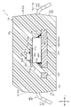
- FIG. 1 is a perspective view of an insulation module of one embodiment.
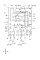
- 2 is a plan view schematically showing the internal structure of the insulation module of FIG. 1.
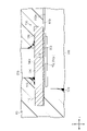
- FIG. 3 is a cross-sectional view of the insulation module of FIG. 2 taken along line 3--3.
- 4 is an enlarged view of a light emitting element and its periphery in the insulation module of FIG. 3.
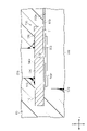
- FIG. 5 is an enlarged view of the light-emitting element, the light-receiving element, and the periphery thereof in the insulation module of FIG. 6 is a cross-sectional view of the insulation module of FIG. 2 taken along line 6--6.
- FIG. 7 is a cross-sectional view schematically showing the internal structure of part of the light emitting device.
- FIG. 8 is a cross-sectional view schematically showing the internal structure of part of the light receiving element.
- 9 is an enlarged plan view of a part of the sealing resin of the insulation module of FIG. 1.
- FIG. 10 is an enlarged plan view of a part different from FIG. 9 of the sealing resin of the insulation module of FIG. 1.
- FIG. 11 is a circuit diagram schematically showing the electrical configuration of the insulation module of FIG. 1.
- FIG. 12 is a plan view showing an enlarged part of the internal structure of the insulation module of the modification.
- FIG. 13 is a cross-sectional view of a plate-like member and its surroundings in an insulation module of a modification.
- FIG. 14 is a cross-sectional view of a plate-like member and its periphery in an insulation module of a modification.
- FIG. 15 is a cross-sectional view of a plate-like member and its surroundings in an insulation module of a modification.
- FIG. 16 is a cross-sectional view of a light-receiving element and its surroundings in an insulation module of a modification.
- FIG. 17 is a cross-sectional view schematically showing the internal structure of part of the light receiving element of the insulation module of the modification.
- FIG. 18 is a cross-sectional view schematically showing the internal structure of part of the light receiving element of the insulation module of the modification.
- FIG. 19 is a circuit diagram schematically showing the electrical configuration of the insulation module of the modification.
- FIG. 20 is a circuit diagram schematically showing the electrical configuration of the insulation module of the modification.
- FIG. 1 and 2 show the overall structure of the isolation module 10.
- FIG. FIG. 3 shows the entire cross-sectional structure inside the insulation module 10
- FIG. 7 shows a partial internal structure of the first light emitting element 20P
- FIG. 8 shows a partial internal structure of the first light receiving element 30P.
- 9 and 10 show the appearance of part of the insulation module 10.
- FIG. FIG. 11 shows an example of the circuit configuration of the insulation module 10. As shown in FIG.
- the insulation module 10 is used for a gate driver that applies a drive voltage signal to the gates of switching elements. As shown in FIGS. 1 and 2, the insulation module 10 has a package structure of DIP (Dual In-line Package).
- the insulation module 10 includes a rectangular sealing resin 80 and a plurality of terminals 41 and 51 projecting from the sealing resin 80 .
- the insulation voltage of the insulation module 10 is, for example, 3500 Vrms or more and 7500 Vrms or less. However, the specific numerical value of the dielectric strength voltage of the insulation module 10 is not limited to this and is arbitrary.
- the encapsulating resin 80 is made of an insulating material with light shielding properties.
- An example of an insulating material is epoxy resin.
- the sealing resin 80 is made of black epoxy resin.
- the thickness direction of the sealing resin 80 is defined as the z-direction, and two mutually orthogonal directions among the directions orthogonal to the z-direction are defined as the x-direction and the y-direction, respectively. Note that the z-direction can also be said to be the "height direction of the insulation module".
- the resin main surface 80s and the resin rear surface 80r constitute both end surfaces of the sealing resin 80 in the thickness direction (z direction). Both the resin main surface 80s and the resin rear surface 80r are formed in a rectangular shape when viewed from the z direction.
- the shape of both the resin main surface 80s and the resin rear surface 80r viewed from the z-direction is a rectangular shape with short sides in the x-direction and long sides in the y-direction.
- the first resin side surface 81 and the second resin side surface 82 form both end surfaces in the x direction. Both the first resin side surface 81 and the second resin side surface 82 extend along the y direction when viewed from the z direction.
- a plurality of (four in this embodiment) terminals 41A to 41D are provided on the first resin side surface 81, and a plurality of (four in this embodiment) terminals 51A to 51D are provided on the second resin side surface 82.
- both the first resin side surface 81 provided with the terminals 41A to 41D and the second resin side surface 82 provided with the terminals 51A to 51D correspond to the "terminal surface".
- a plurality of terminals 41A to 41D protrude from the first resin side surface 81.
- a plurality of terminals 51A to 51D protrude from the second resin side surface . Therefore, when viewed from the z direction, it can be said that the plurality of terminals 41A to 41D and the plurality of terminals 51A to 51D are arranged side by side at intervals in the x direction. In other words, the x direction can also be said to be the direction in which the terminals 41A to 41D and the terminals 51A to 51D are arranged.
- the plurality of terminals 51A-51D have the same shape as the plurality of terminals 41A-41D. In this manner, the plurality of terminals 41A to 41D are provided side by side on the first resin side surface 81, and the plurality of terminals 51A to 51D are provided side by side on the second resin side surface .
- the third resin side surface 83 and the fourth resin side surface 84 constitute both end surfaces in the y direction. Both the third resin side surface 83 and the fourth resin side surface 84 are side surfaces on which the plurality of terminals 41A to 41D and 51A to 51D are not provided. Both the third resin side surface 83 and the fourth resin side surface 84 extend along the x direction when viewed from the z direction.
- each of the terminals 41A to 41D and 51A to 51D have the same shape. More specifically, as shown in FIG. 1, each of the terminals 41A to 41D has a first portion extending in the x direction from the first resin side surface 81, a first bent portion bent downward from the first portion, and an x a second portion extending so as to incline downward as it moves away from the sealing resin 80 in the direction; a second bent portion that is bent outward from the second portion; and a third portion extending at an angle. The tilt angle of the third portion with respect to the z-direction is smaller than the tilt angle of the second portion with respect to the z-direction.
- each of the terminals 41A-41D and 51A-51D has a so-called gull-wing type terminal.
- the plurality of terminals 41A to 41D and 51A to 51D constitute external terminals mounted on lands provided on the wiring board (not shown) when the insulation module 10 is mounted on the wiring board, for example.
- the terminals 41A to 41D and 51A to 51D are joined to the lands of the wiring board by a conductive joining material formed of solder, Ag (silver) paste, or the like. Thereby, the insulation module 10 is electrically connected to the wiring board.
- Each resin side surface 81-84 has a first side surface 85 and a second side surface 86.
- the first side surface 85 is continuous with the second side surface 86 .
- the first side surface 85 is arranged closer to the resin main surface 80s than the resin back surface 80r in the z-direction.
- the second side surface 86 is arranged closer to the resin rear surface 80r than the resin main surface 80s in the z-direction.
- the first side surface 85 of the first resin side surface 81 and the first side surface 85 of the second resin side surface 82 are inclined so as to approach each other in the x direction toward the resin main surface 80s.
- the side surface 86 and the second side surface 86 of the second resin side surface 82 are inclined so as to approach each other in the x direction toward the resin back surface 80r.
- a first side surface 85 (not shown) of the third resin side surface 83 and a first side surface 85 of the fourth resin side surface 84 are inclined toward each other in the y direction toward the resin main surface 80s.
- a second side surface 86 (not shown) of 83 and a second side surface 86 of the fourth resin side surface 84 are inclined so as to approach each other in the y direction toward the resin back surface 80r.
- the four terminals 41A to 41D protrude from between the first side surface 85 and the second side surface 86 of the first resin side surface 81 respectively.
- the four terminals 41A-41D are arranged apart from each other in the y direction.
- the four terminals 51A to 51D protrude from between the first side surface 85 and the second side surface 86 of the second resin side surface 82 respectively.
- the four terminals 51A to 51D are arranged apart from each other in the y direction.
- FIG. 2 is a plan view of the insulation module 10 showing the internal structure of the insulation module 10. As shown in FIG. In FIG. 2, the sealing resin 80 is indicated by a chain double-dashed line for convenience.
- the insulation module 10 includes a first light emitting element 20P and a second light emitting element 20Q, a first light receiving element 30P and a second light receiving element 30Q, a first lead frame 40 and a second lead frame 50. and has.
- a first photocoupler is composed of the first light emitting element 20P and the first light receiving element 30P
- a second photocoupler is composed of the second light emitting element 20Q and the second light receiving element 30Q.
- the sealing resin 80 seals at least the light emitting elements 20P and 20Q and the light receiving elements 30P and 30Q.
- the first lead frame 40 is a lead frame electrically connected to the first light receiving element 30P
- the second lead frame 50 is a lead frame electrically connected to the second light receiving element 30Q.
- the first lead frame 40 includes first lead frames 40A to 40D as four first lead frames.
- the first lead frames 40A to 40D are arranged apart from each other in the y direction when viewed from the z direction.
- the first lead frame 40A is arranged closer to the third resin side surface 83 than the first lead frames 40B to 40D.
- the first lead frame 40A includes terminals 41A.
- the terminal 41A is a portion of the first lead frame 40A protruding from the first resin side surface 81 to the outside of the sealing resin 80 .
- Inner leads 42A which are portions of the first lead frame 40A provided in the sealing resin 80, have lead portions 42AA and wire connection portions 42AB.
- the lead portion 42AA is a portion continuous with the terminal 41A and extends in the x direction.
- a wire connecting portion 42AB is provided at the tip of the lead portion 42AA.
- the wire connecting portion 42AB has a portion extending in the y direction toward the fourth resin side surface 84 with respect to the lead portion 42AA. That is, the wire connection portion 42AB has a portion protruding toward the fourth resin side surface 84 with respect to the lead portion 42AA.
- the sealing resin 80 exists on both sides of the wire connecting portion 42AB in the x direction. Therefore, it is possible to prevent the first lead frame 40A from moving in the x direction with respect to the sealing resin 80 by the wire connecting portion 42AB.
- the first lead frame 40B is arranged near the fourth resin side surface 84 with respect to the first lead frame 40A.
- the first lead frame 40B includes terminals 41B. That is, the terminal 41B is a portion of the first lead frame 40B protruding from the first resin side surface 81 to the outside of the sealing resin 80 .
- Inner leads 42B which are portions of the first lead frame 40B provided in the sealing resin 80, have lead portions 42BA and wire connection portions 42BB.
- the lead portion 42BA is a portion continuous with the terminal 41B and extends in the x direction.
- a wire connecting portion 42BB is provided at the tip of the lead portion 42BA.
- the wire connection portion 42BB has a portion extending in the y direction toward the fourth resin side surface 84 with respect to the lead portion 42BA. That is, the wire connection portion 42BB has a portion protruding toward the fourth resin side surface 84 with respect to the lead portion 42BA.
- the length of the wire connection portion 42BB in the y direction is longer than the length of the wire connection portion 42AB in the y direction.
- the sealing resin 80 exists on both sides of the wire connection portion 42BB in the x direction. Therefore, it is possible to suppress the movement of the first lead frame 40B in the x direction with respect to the sealing resin 80 by the wire connection portion 42BB.
- the first lead frame 40C is arranged near the fourth resin side surface 84 with respect to the first lead frame 40B.
- the first lead frame 40C includes terminals 41C. That is, the terminal 41C is a portion of the first lead frame 40C protruding from the first resin side surface 81 to the outside of the sealing resin 80 .
- Inner leads 42C which are portions of the first lead frame 40C provided in the sealing resin 80, have lead portions 42CA and wire connection portions 42CB.
- the lead portion 42CA is a portion continuous with the terminal 41C and extends in the x direction.
- a wire connecting portion 42CB is provided at the tip of the lead portion 42CA.
- the wire connection portion 42CB has portions extending on both sides in the y direction with respect to the lead portion 42CA.
- the wire connection portion 42CB has portions protruding toward both sides in the y direction with respect to the lead portion 42CA.
- the length of the wire connection portion 42CB in the y direction is longer than the length of the wire connection portion 42BB in the y direction.
- the sealing resin 80 exists on both sides of the wire connecting portion 42CB in the x direction. Therefore, it is possible to prevent the first lead frame 40C from moving in the x direction with respect to the sealing resin 80 by the wire connecting portion 42CB.
- the first lead frame 40D is arranged near the fourth resin side surface 84 with respect to the first lead frame 40C.
- the first lead frame 40D includes terminals 41D. That is, the terminal 41D is a portion of the first lead frame 40D protruding from the first resin side surface 81 to the outside of the sealing resin 80. As shown in FIG.
- the inner lead 42D which is the portion of the first lead frame 40D provided in the sealing resin 80, has a lead portion 42DA and a die pad portion 42DB.
- the die pad portion 42DB corresponds to the "die pad”.
- the lead portion 42DA is a portion continuous with the terminal 41D and has a first portion 43D extending in the x direction and a second portion 44D extending in the y direction.
- the first portion 43D is continuous with the terminal 41D.
- the second portion 44D is a portion that connects the first portion 43D and the die pad portion 42DB.
- the second portion 44D is arranged closer to the second resin side surface 82 than the first lead frames 40A to 40C. When viewed in the x direction, the second portion 44D extends to a position overlapping the first lead frame 40C.
- the width of the second portion 44D (the length of the second portion 44D in the y direction) is narrower than the width of the first portion 43D (the length of the first portion 43D in the x direction).
- the die pad portion 42DB is arranged closer to the third resin side surface 83 than the center of the sealing resin 80 in the y direction.
- the die pad portion 42DB is arranged closer to the second resin side surface 82 than the first lead frames 40A to 40C in the x direction.
- the shape of the die pad portion 42DB viewed from the z direction is a rectangular shape with long sides in the x direction and short sides in the y direction.
- the die pad portion 42DB is provided so as to overlap the first lead frames 40A and 40B when viewed in the x direction.
- a protrusion 45D and a suspension lead 46D are provided on the die pad portion 42DB.
- the protrusion 45D extends in the x-direction toward the second resin side surface 82 from a corner near the second resin side surface 82 and the third resin side surface 83 among the four corners of the die pad portion 42DB.
- the width of the projection 45D (the length of the projection 45D in the y direction) is equal to the width of the lead portion 42AA (the length of the lead portion 42AA in the y direction). That is, the width of the projection 45D is wider than the width of the second portion 44D.
- the suspension lead 46D extends in the x-direction toward the first resin side surface 81 from the end closer to the first resin side surface 81 among the x-direction end portions of the die pad portion 42DB.
- the tip of the suspension lead 46 ⁇ /b>D is exposed from the first resin side surface 81 .
- the suspension lead 46D is arranged between the first lead frame 40A and the first lead frame 40B in the y direction. That is, the portion of the suspension lead 46D exposed from the first resin side surface 81 is located between the terminal 41A and the terminal 41B in the y direction.
- the second lead frame 50 includes second lead frames 50A to 50D as four second lead frames.
- the second lead frames 50A to 50D are arranged apart from each other in the y direction when viewed from the z direction.
- the second lead frame 50A is arranged closer to the third resin side surface 83 than the second lead frames 50B to 50D.
- the second lead frame 50A includes terminals 51A.
- the terminal 51A is a portion of the second lead frame 50A protruding outside the sealing resin 80 from the second resin side surface 82 .
- the terminal 51A is arranged at a position overlapping the terminal 41A when viewed in the x direction.
- Inner leads 52A which are portions of the second lead frame 50A provided in the sealing resin 80, have lead portions 52AA and wire connection portions 52AB.
- the lead portion 52AA is a portion continuous with the terminal 51A and extends in the x direction.
- a wire connecting portion 52AB is provided at the tip of the lead portion 52AA.
- the wire connection portion 52AB has a portion extending in the y direction toward the fourth resin side surface 84 with respect to the lead portion 52AA. That is, the wire connecting portion 52AB has a portion protruding toward the fourth resin side surface 84 with respect to the lead portion 52AA.
- the y-direction length of the wire connection portion 52AB is longer than the y-direction length of the wire connection portion 42AB of the first lead frame 40A.
- the y-direction length of the wire connection portion 52AB is longer than the y-direction length of the wire connection portion 42CB of the first lead frame 40C.
- the lead portion 52AA and the wire connection portion 52AB are arranged at positions facing the protrusion 45D of the first lead frame 40D in the x direction.
- the wire connecting portion 52AB is arranged closer to the second resin side surface 82 than the projection 45D.
- the sealing resin 80 exists on both sides of the wire connecting portion 52AB in the x direction. Therefore, it is possible to suppress the movement of the second lead frame 50A in the x-direction with respect to the sealing resin 80 by the wire connecting portion 52AB.
- the second lead frame 50B is arranged closer to the fourth resin side surface 84 than the second lead frame 50A.
- the second lead frame 50B includes terminals 51B. That is, the terminal 51B is a portion of the second lead frame 50B protruding from the second resin side surface 82 to the outside of the sealing resin 80 . In this embodiment, the terminal 51B is arranged at a position overlapping the terminal 41B when viewed in the x direction.
- Inner leads 52B which are portions of the second lead frame 50B provided in the sealing resin 80, have lead portions 52BA and wire connection portions 52BB.
- the lead portion 52BA is a portion continuous with the terminal 51B and extends in the x direction.
- a wire connecting portion 52BB is provided at the tip of the lead portion 52BA.
- the wire connection portion 52BB has a portion extending in the y direction toward the fourth resin side surface 84 with respect to the lead portion 52BA. That is, the wire connection portion 52BB has a portion protruding toward the fourth resin side surface 84 with respect to the lead portion 52BA.
- the y-direction length of the wire connection portion 52BB is shorter than the y-direction length of the wire connection portion 52AB of the second lead frame 50A.
- the lead portion 52BA and the wire connection portion 52BB are arranged at positions facing the die pad portion 42DB of the first lead frame 40D in the x direction.
- the wire connection portion 52BB is arranged closer to the second resin side surface 82 than the projection 45D.
- the sealing resin 80 exists on both sides of the wire connection portion 52BB in the x direction. Therefore, it is possible to suppress the movement of the second lead frame 50B in the x-direction with respect to the sealing resin 80 by the wire connection portion 52BB.
- the second lead frame 50C is arranged closer to the fourth resin side surface 84 than the second lead frame 50B.
- the second lead frame 50C includes terminals 51C.
- the terminal 51C is a portion of the second lead frame 50C protruding outside the sealing resin 80 from the second resin side surface 82 .
- the terminal 51C is arranged at a position overlapping the terminal 41C when viewed in the x direction.
- Inner leads 52C which are portions of the second lead frame 50C provided in the sealing resin 80, have lead portions 52CA and wire connection portions 52CB.
- the lead portion 52CA is a portion continuous with the terminal 51C and extends in the x direction.
- a wire connecting portion 52CB is provided at the tip of the lead portion 52CA.
- the wire connection portion 52CB has a portion extending in the y direction toward the fourth resin side surface 84 with respect to the lead portion 52CA. That is, the wire connection portion 52CB has a portion protruding toward the fourth resin side surface 84 with respect to the lead portion 52CA.
- the y-direction length of the wire connection portion 52CB is shorter than the y-direction length of the wire connection portion 52BB of the second lead frame 50B.
- the lead portion 52CA and the wire connection portion 52CB are arranged closer to the side surface of the fourth resin than the die pad portion 42DB of the first lead frame 40D in the x direction.
- the wire connection portion 52CB is arranged closer to the second resin side surface 82 than the die pad portion 42DB.
- the sealing resin 80 exists on both sides of the wire connection portion 52CB in the x direction. Therefore, it is possible to suppress the movement of the second lead frame 50C in the x-direction with respect to the sealing resin 80 by the wire connection portion 52CB.
- the second lead frame 50D is arranged closer to the fourth resin side surface 84 than the second lead frame 50C.
- the second lead frame 50D includes terminals 51D. That is, the terminal 51D is a portion of the second lead frame 50D protruding from the second resin side surface 82 to the outside of the sealing resin 80 . In this embodiment, the terminal 51D is arranged at a position overlapping the terminal 41D when viewed in the x direction.
- An inner lead 52D which is a portion of the second lead frame 50D provided in the sealing resin 80, has a lead portion 52DA, a die pad portion 52DB, and a wire connection portion 52DC.
- the lead portion 52DA is a portion continuous with the terminal 51D and extends in the x direction.
- the length of the lead portion 52DA in the x direction is longer than the length of the lead portions 52AA to 52CA in the x direction.
- the lead portion 52DA is connected to the die pad portion 52DB.
- the die pad portion 52DB is arranged closer to the fourth resin side surface 84 than the center of the sealing resin 80 in the y direction. It can also be said that the die pad portion 52DB is arranged closer to the fourth resin side surface 84 than the die pad portion 42DB of the first lead frame 40D.
- the die pad portion 52DB is arranged side by side with the die pad portion 42DB in the y direction.
- the die pad portion 52DB is arranged closer to the first resin side surface 81 than the second lead frames 50A to 50C in the x direction.
- the shape of the die pad portion 52DB viewed from the z direction is a rectangular shape with short sides in the x direction and long sides in the y direction.
- the die pad portion 52DB is provided so as to overlap the second lead frame 50C when viewed in the x direction.
- a wire connection portion 52DC is provided at a corner near the third resin side surface 83 and the second resin side surface 82 among the four corners of the die pad portion 52DB.
- the wire connection portion 52DC extends in the y-direction from the die pad portion 52DB toward the third resin side surface 83.
- the wire connection portion 52DC is arranged closer to the second resin side surface 82 than the die pad portion 42DB of the first lead frame 40D, and is arranged at a position overlapping the die pad portion 42DB when viewed in the x direction.
- the wire connection portion 52DC is arranged closer to the first resin side surface 81 than the second lead frames 50A and 50B, and is arranged at a position overlapping the second lead frames 50A and 50B when viewed from the x direction. That is, the wire connection portion 52DC is arranged between the die pad portion 42DB and the second lead frames 50A and 50B in the x direction.
- a wire connection portion 53D is provided in a portion of the lead portion 52DA near the die pad portion 52DB.
- the wire connecting portion 53D is a portion extending in the y-direction from the lead portion 52DA toward the third resin side surface 83. As shown in FIG.
- the wire connection portion 53D is arranged at a position aligned with the wire connection portion 52CB of the second lead frame 50C in the x direction.
- a through hole 54D is provided in a portion of the die pad portion 52DB near the fourth resin side surface 84 .
- the through hole 54D is provided at a position overlapping the lead portion 52DA when viewed from the x direction.
- a sealing resin 80 is filled in the through hole 54D. The sealing resin 80 in the through hole 54D can prevent the second lead frame 50D from moving with respect to the sealing resin 80 in the direction perpendicular to the z direction.
- the first light receiving element 30P is mounted on the die pad portion 42DB of the first lead frame 40D
- the second light receiving element 30Q is mounted on the die pad portion 52DB of the second lead frame 50D
- the first light emitting element 20P is mounted on the first light receiving element 30P
- the second light emitting element 20Q is mounted on the second light receiving element 30Q.
- the first light receiving element 30P and the second light receiving element 30Q are light receiving elements having the same shape and size. Light emitting elements having the same shape and size are used for the first light emitting element 20P and the second light emitting element 20Q.
- the die pad portion 42DB corresponds to the "first die pad”
- the die pad portion 52DB corresponds to the "second die pad”.
- the first light receiving element 30P is arranged biased toward the second resin side surface 82 with respect to the die pad portion 42DB. That is, the center of the first light receiving element 30P in the x direction is positioned closer to the second resin side surface 82 than the center of the die pad portion 42DB in the x direction. In this embodiment, the first light receiving element 30P is arranged closer to the second resin side surface 82 than the lead portion 42DA in the x direction.
- the first light receiving element 30P is joined to the die pad portion 42DB with a conductive joining material 100P (see FIG. 6) such as solder or Ag (silver) paste.
- the first light receiving element 30P is joined to the die pad portion 42DB by being die-bonded to the die pad portion 42DB.
- the shape of the first light receiving element 30P viewed from the z direction is a rectangular shape with short sides in the x direction and long sides in the y direction.
- the conductive bonding material 100P corresponds to the "light receiving bonding material”.
- the second light receiving element 30Q is arranged biased toward the first resin side surface 81 with respect to the die pad portion 52DB. That is, the center of the second light receiving element 30Q in the x direction is positioned closer to the first resin side surface 81 than the center of the die pad portion 52DB in the x direction. In this embodiment, the second light receiving element 30Q is arranged closer to the first resin side surface 81 than the wire connecting portion 52DC in the x direction.
- the second light receiving element 30Q is bonded to the die pad portion 52DB with a conductive bonding material 100Q (see FIG. 6) such as solder or Ag paste.
- the second light receiving element 30Q is joined to the die pad portion 52DB by being die-bonded to the die pad portion 52DB.
- the conductive bonding material 100Q corresponds to the "light receiving bonding material".
- the first light receiving element 30P and the second light receiving element 30Q are arranged side by side in the y direction. More specifically, the first light-receiving element 30P and the second light-receiving element 30Q are arranged to overlap each other when viewed in the y direction. On the other hand, the first light-receiving element 30P and the second light-receiving element 30Q are arranged to be offset from each other in the x direction. The first light receiving element 30P is arranged so as to be shifted toward the first resin side surface 81 with respect to the second light receiving element 30Q in the x direction.
- the end portion closer to the first resin side surface 81 is arranged closer to the first resin side surface 81 than the second light receiving element 30Q when viewed from the y direction.
- the second light receiving element 30Q is arranged shifted toward the second resin side surface 82 with respect to the first light receiving element 30P in the x direction. That is, of the x-direction end portions of the second light receiving element 30Q, the end portion closer to the second resin side surface 82 is arranged closer to the second resin side surface 82 than the first light receiving element 30P when viewed from the y direction. ing.
- the first light emitting element 20P is arranged at a position overlapping the first light receiving element 30P when viewed from the z direction. More specifically, the first light emitting element 20P is arranged closer to the second resin side surface 82 than the center of the first light receiving element 30P in the x direction when viewed in the z direction. Among both edges of the first light emitting element 20P in the x direction, the edge closer to the second resin side surface 82 is the edge closer to the second resin side surface 82 than both edges of the first light receiving element 30P in the x direction. is arranged closer to the first resin side surface 81 than the first resin side surface 81 .
- the edge closer to the first resin side surface 81 is arranged closer to the second resin side surface 82 than the center of the first light receiving element 30P in the x direction.
- the first light emitting element 20P is arranged closer to the third resin side surface 83 than the center of the first light receiving element 30P in the y direction when viewed from the z direction. More specifically, when viewed from the z direction, the first light emitting element 20P is arranged at a position overlapping the first virtual line VL1 extending along the x direction at the center of the first light receiving element 30P in the y direction.
- the y-direction center of the first light emitting element 20P is arranged closer to the third resin side surface 83 than the first virtual line VL1.
- the shape of the first light emitting element 20P viewed from the z direction is a rectangular shape with short sides in the x direction and long sides in the y direction.
- the area of the first light emitting element 20P is smaller than half the area of the first light receiving element 30P.
- the area of the first light emitting element 20P is larger than 1/10 of the area of the first light receiving element 30P and smaller than 1/2 of the area of the first light receiving element 30P.
- the area of the first light emitting element 20P is about 1/9 of the area of the first light receiving element 30P when viewed from the z direction.
- the first light emitting element 20P has an element main surface 20Ps and an element rear surface 20Pr facing opposite sides in the thickness direction of the first light emitting element 20P.
- the element main surface 20Ps faces the same side as the pad main surface 42Ds of the die pad portion 42DB, and the element rear surface 20Pr faces the same side as the pad rear surface 42Dr.
- the element rear surface 20Pr constitutes the light emitting surface of the first light emitting element 20P. Therefore, the element main surface 20Ps corresponds to "the back surface facing away from the light emitting surface".
- the second light emitting element 20Q is arranged at a position overlapping the second light receiving element 30Q when viewed from the z direction. More specifically, the second light emitting element 20Q is arranged closer to the first resin side surface 81 than the center of the second light receiving element 30Q in the x direction when viewed in the z direction. Of the x-direction edges of the second light emitting element 20Q, the edge closer to the first resin side surface 81 is the edge of the x-direction edge of the second light receiving element 30Q that is closer to the first resin side surface 81. It is arranged closer to the second resin side surface 82 than the second resin side surface 82 .
- the edge closer to the second resin side surface 82 is arranged closer to the first resin side surface 81 than the center of the second light receiving element 30Q in the x direction.
- the second light emitting element 20Q is arranged closer to the fourth resin side surface 84 than the center of the second light receiving element 30Q in the y direction when viewed from the z direction. More specifically, when viewed from the z direction, the second light emitting element 20Q is arranged at a position overlapping the second virtual line VL2 extending along the x direction at the center of the second light receiving element 30Q in the y direction.
- the center of the second light emitting element 20Q in the y direction is arranged closer to the fourth resin side surface 84 than the second virtual line VL2. Note that the relationship between the area of the second light emitting element 20Q and the area of the second light receiving element 30Q when viewed from the z-direction is the same as that of the first light emitting element 20P and the first light receiving element 30P, so detailed description is omitted. .
- the first light emitting element 20P has an element main surface 20Qs and an element rear surface 20Qr facing opposite sides in the thickness direction of the second light emitting element 20Q.
- the element main surface 20Qs faces the same side as the pad main surface 52Ds of the die pad portion 52DB, and the element rear surface 20Qr faces the same side as the pad rear surface 52Dr.
- the element rear surface 20Qr constitutes the light emitting surface of the second light emitting element 20Q. Therefore, the element main surface 20Qs corresponds to "the back surface facing away from the light emitting surface".
- the first light emitting element 20P and the second light emitting element 20Q are arranged apart from each other in the y direction.
- the first light emitting element 20P is arranged closer to the second resin side surface 82 than the second light emitting element 20Q.
- the second light emitting element 20Q is arranged closer to the first resin side surface 81 than the first light emitting element 20P.
- the first light emitting element 20P and the second light emitting element 20Q are arranged at positions that do not overlap each other.
- the first light emitting element 20P emits light of a first wavelength.
- An example of light of the first wavelength is light of wavelengths including infrared.
- the second light emitting element 20Q emits light of a second wavelength different from the first wavelength.
- An example of light of the second wavelength is light of wavelengths including red. Both the first light emitting element 20P and the second light emitting element 20Q emit light downward.
- the first light receiving element 30P is configured to be able to receive light (light of the first wavelength) from the first light emitting element 20P.
- the first light receiving element 30P includes a first semiconductor region that receives light from the first light emitting element 20P and a second semiconductor region that generates a signal based on the received light.
- a photoelectric conversion element is provided in the first semiconductor region. Photodiodes, for example, are used as photoelectric conversion elements.
- the second semiconductor region is formed by, for example, LSI (Large Scale Integration). That is, the first light receiving element 30P of the present embodiment is an element in which the function of receiving light from the first light emitting element 20P and the function of generating a signal from the received light are integrated.
- the first semiconductor region and the second semiconductor region are formed side by side in the x-direction.
- the first semiconductor region is formed in a portion of the first light receiving element 30P which overlaps with the first light emitting element 20P when viewed from the z direction.
- the first light emitting element 20P is arranged biased toward the photoelectric conversion element with respect to the first light receiving element 30P.
- the second semiconductor region is formed in a portion of the first light receiving element 30P near the second resin side surface 82 when viewed in the z direction.
- the area of the first semiconductor region viewed in the z-direction is smaller than the area of the second semiconductor region viewed in the z-direction.
- the x-direction dimension of the first semiconductor region is smaller than the x-direction dimension of the second semiconductor region.
- the first semiconductor region of the first light receiving element 30P forms a light receiving surface 33P. That is, the first light emitting element 20P is arranged at a position overlapping the light receiving surface 33P of the first light receiving element 30P when viewed from the z direction. Therefore, the light receiving surface 33P of the first light receiving element 30P faces the element rear surface 20Pr (light emitting surface) of the first light emitting element 20P.
- the second light receiving element 30Q is configured to receive light (light of the second wavelength) from the second light emitting element 20Q. Since the second light receiving element 30Q has the same configuration as the first light receiving element 30P, detailed description thereof will be omitted.
- the second light receiving element 30Q similarly has a light receiving surface 33Q as a first semiconductor region.
- the second light-emitting element 20Q is arranged at a position overlapping the light-receiving surface 33Q of the second light-receiving element 30Q when viewed from the z-direction. Therefore, the light receiving surface 33Q of the second light receiving element 30Q faces the element rear surface 20Qr (light emitting surface) of the second light emitting element 20Q. Also, the second light emitting element 20Q is arranged biased toward the photoelectric conversion element with respect to the second light receiving element 30Q.
- the first light receiving element 30P has an element main surface 30Ps and an element back surface 30Pr facing opposite sides in the thickness direction of the first light receiving element 30P.
- the element main surface 30Ps faces the same side as the pad main surface 42Ds of the die pad portion 42DB, and the element rear surface 30Pr faces the same side as the pad rear surface 42Dr.
- the element main surface 30Ps includes a light receiving surface 33P. Therefore, in this embodiment, the back surface 30Pr of the element constitutes "the back surface facing away from the light receiving surface". Further, the element main surface 30Ps faces the same side as the resin main surface 80s (see FIG. 3) of the sealing resin 80, and the element rear surface 30Pr faces the same side as the resin rear surface 80r (see FIG.
- the sealing resin 80 there is That is, the light receiving surface 33P faces the same side as the resin main surface 80s, and the element rear surface 20Pr of the first light emitting element 20P, which is the light emitting surface facing the light receiving surface 33P, faces the same side as the resin rear surface 80r.
- the second light receiving element 30Q has an element main surface 30Qs and an element back surface 30Qr facing opposite sides in the thickness direction of the second light receiving element 30Q.
- the element main surface 30Qs faces the same side as the pad main surface 52Ds of the die pad portion 52DB, and the element rear surface 30Qr faces the same side as the pad rear surface 52Dr.
- the element main surface 30Qs includes a light receiving surface 33Q. Therefore, in this embodiment, the back surface 30Qr of the element constitutes "the back surface facing away from the light receiving surface".
- the element main surface 30Qs faces the same side as the resin main surface 80s of the sealing resin 80, and the element rear surface 30Qr faces the same side as the resin rear surface 80r of the sealing resin 80.
- the light receiving surface 33Q faces the same side as the resin main surface 80s
- the element rear surface 20Qr of the second light emitting element 20Q which is the light emitting surface facing the light receiving surface 33Q, faces the same side as the resin rear surface 80r.
- the light of the first wavelength from the first light emitting element 20P and the light of the second wavelength from the second light emitting element 20Q can be changed arbitrarily.
- both the first light emitting element 20P and the second light emitting element 20Q may be configured to emit visible light.
- the first light emitting element 20P may be configured to emit light of wavelengths including blue
- the second light emitting element 20Q may be configured to emit light of wavelengths including red.
- the light of the first wavelength from the first light emitting element 20P and the light of the second wavelength from the second light emitting element 20Q are lights having different wavelengths, but the present invention is not limited to this.
- the first light emitting element 20P and the second light emitting element 20Q may be configured to emit light of the same wavelength. In one example, both the first light emitting element 20P and the second light emitting element 20Q are configured to emit light including red wavelengths. In another example, both the first light emitting element 20P and the second light emitting element 20Q are configured to emit light of wavelengths including infrared rays.
- the configuration of the die pad portion 42DB, the first light emitting element 20P, and the first light receiving element 30P, and the layout of the die pad portion 42DB, the first light receiving element 30P, and the first light emitting element 20P are the second light emitting element 20Q, Since it is similar to the second light receiving element 30Q and the die pad portion 52DB, detailed description thereof will be omitted.
- the internal structures of the second light emitting element 20Q and the second light receiving element 30Q are omitted.
- the die pad portion 52DB is arranged closer to the resin back surface 80r than the position where the terminal 51D projects from the second resin side surface 82 in the z direction. Therefore, the lead portion 52DA has a portion that is bent toward the resin back surface 80r toward the die pad portion 52DB.
- the die pad portion 52DB has a pad main surface 52Ds and a pad rear surface 52Dr facing opposite sides in the thickness direction.
- the pad main surface 52Ds is a surface forming a mounting surface on which the second light receiving element 30Q is mounted, and faces the same side as the resin main surface 80s.
- the pad back surface 52Dr faces the same side as the resin back surface 80r.
- the pad back surface 52Dr is arranged apart from the resin back surface 80r in the z direction. That is, the pad rear surface 52Dr is not exposed from the resin rear surface 80r.
- the die pad portion 52DB has a main metal layer 55D and a plated layer 56D formed on the outer surface of the main metal layer 55D.
- the main metal layer 55D is made of a metal material containing Cu, for example.
- the plated layer 56D is made of a material containing Ni (nickel), Cr (chromium), or the like. As shown in FIG. 5, the plating layer 56D is sufficiently thin compared to the main metal layer 55D.
- the conductive bonding material 100Q that bonds the second light receiving element 30Q and the die pad portion 52DB is a first bonding region 101Q interposed between the element rear surface 30Qr of the second light receiving element 30Q and the pad main surface 52Ds of the die pad portion 52DB. , and a second junction region 102Q that protrudes from the second light receiving element 30Q when viewed in the z direction and is joined to the outer surface of the second light receiving element 30Q.
- the second junction region 102Q is provided so that the thickness of the second junction region 102Q becomes thinner as the distance from the outer surface of the second light receiving element 30Q increases.
- the second junction region 102Q is formed over the entire circumference of the second light receiving element 30Q when viewed from the z direction.
- the height HT of the portion of the second junction region 102Q in contact with the outer surface of the second light receiving element 30Q is higher than 1/2 or less of the height HRQ of the second light receiving element 30Q.
- the height HT is about 2/3 of the height HRQ.
- the height HT is defined by the height from the pad main surface 52Ds of the die pad portion 52DB of the portion of the second junction region 102Q in contact with the outer side surface of the second light receiving element 30Q. That is, it can be said that the height HT is the thickness of the portion of the second junction region 102Q that is in contact with the outer side surface of the second light receiving element 30Q.
- the height HRQ is defined by the distance in the z direction between the pad main surface 52Ds of the die pad portion 52DB and the element main surface 30Qs of the second light receiving element 30Q.
- the conductive bonding material 100P that bonds the first light receiving element 30P and the die pad portion 42DB has a first bonding region 101P and a second bonding region 102P (see FIG. 6) like the conductive bonding material 100Q. reference).
- the first bonding region 101P is interposed between the element rear surface 30Pr of the first light receiving element 30P and the pad main surface 42Ds of the die pad portion 42DB.
- the second bonding region 102P is a region protruding from the first light receiving element 30P when viewed in the z direction and is bonded to the outer side surface of the first light receiving element 30P. Note that the first bonding region 101P and the second bonding region 102P are the same as the conductive bonding material 100Q, so detailed description thereof will be omitted.
- the insulation module 10 includes a first plate member 70P laminated on the first light receiving element 30P, a second plate member 70Q laminated on the second light receiving element 30Q, and a first plate member 70Q.
- both the first plate-like member 70P and the second plate-like member 70Q correspond to the "insulating member". Both the first plate member 70P and the second plate member 70Q have translucency.
- the first light emitting element 20P is arranged on the first plate member 70P, and the second light emitting element 20Q is arranged on the second plate member 70Q. That is, the first plate member 70P and the first transparent resin 60P are interposed between the first light emitting element 20P and the first light receiving element 30P in the z direction, and the second light emitting element 20Q and the second light receiving element 30Q are interposed. A second plate member 70Q and a second transparent resin 60Q are interposed between them in the z direction.
- the first transparent resin 60P is formed on the element main surface 30Ps of the first light receiving element 30P. At least part of the first transparent resin 60P is provided on the light receiving surface 33P. In this embodiment, the first transparent resin 60P is formed, for example, over the entire element main surface 30Ps.
- the first transparent resin 60P is a bonding material that bonds the first plate member 70P to the element main surface 30Ps of the first light receiving element 30P.
- the second transparent resin 60Q is formed on the element main surface 30Qs of the second light receiving element 30Q. At least part of the second transparent resin 60Q is provided on the light receiving surface 33Q. In this embodiment, the second transparent resin 60Q is formed, for example, over the entire element main surface 30Qs.
- the second transparent resin 60Q is a bonding material that bonds the second plate member 70Q to the element main surface 30Qs of the second light receiving element 30Q.
- the transparent resins 60P and 60Q insulating materials such as transparent epoxy resin, acrylic resin, and silicone resin are used.
- the first transparent resin 60P is made of an insulating resin through which light (light of the first wavelength) from the first light emitting element 20P can pass.
- the first transparent resin 60P is made of an insulating resin that blocks (does not transmit) the light from the second light emitting element 20Q.
- the second transparent resin 60Q is made of an insulating resin through which light (light of the second wavelength) from the second light emitting element 20Q can pass.
- the second transparent resin 60Q is made of an insulating resin that blocks (does not transmit) the light from the first light emitting element 20P.
- Each transparent resin 60P, 60Q is formed by potting, for example.
- the first plate-like member 70P has a main surface 70Ps and a back surface 70Pr facing opposite sides in the thickness direction.
- the main surface 70Ps faces the same side as the element main surface 30Ps of the first light receiving element 30P
- the rear surface 70Pr faces the same side as the element rear surface 30Pr of the first light receiving element 30P.
- the first plate-like member 70P is in contact with the first transparent resin 60P on the rear surface 70Pr.
- the main surface 70Ps of the first plate member 70P corresponds to the "first surface”
- the rear surface 70Pr corresponds to the "second surface”.
- the first plate member 70P is arranged so as to overlap the first semiconductor region of the first light receiving element 30P.
- the first plate member 70P covers the light receiving surface 33P of the first light receiving element 30P. It can be said that the first plate member 70P is laminated at least on the light receiving surface 33P (see FIG. 2) of the first light receiving element 30P. Therefore, it can be said that the back surface 70Pr of the first plate member 70P faces the light receiving surface 33P.
- the first plate member 70P is arranged to be biased in the x direction with respect to the first light receiving element 30P. More specifically, the first plate-like member 70P is arranged biased toward the second resin side surface 82 with respect to the first light receiving element 30P. The first plate member 70P is arranged closer to the second resin side surface 82 than the wires WB1 to WB4. In one example, the y-direction length of the first plate member 70P is longer than the y-direction length of the first light receiving element 30P.
- the thickness T1 of the second plate member 70Q is thicker than the thickness T2 of the second transparent resin 60Q.
- the thickness T2 of the second transparent resin 60Q is thinner than the thickness T1 of the second plate member 70Q.
- the thickness T1 of the second plate member 70Q is, for example, two to five times the thickness T2 of the second transparent resin 60Q. In this embodiment, the thickness T1 of the second plate member 70Q is approximately four times the thickness T2 of the second transparent resin 60Q.
- the relationship between the thickness of the first plate member 70P and the thickness of the first transparent resin 60P is the same as the relationship between the thickness T1 of the second plate member 70Q and the thickness T2 of the second transparent resin 60Q. .
- the first plate member 70P can be divided into a first extending portion 71P, a second extending portion 72P, and an intermediate portion 73P in the x direction.
- the intermediate portion 73P is provided between the first extension portion 71P and the second extension portion 72P in the x direction, and connects the first extension portion 71P and the second extension portion 72P.
- the first extending portion 71P is a portion protruding toward the first resin side surface 81 with respect to the first light emitting element 20P when viewed in the z direction.
- the second extending portion 72P is a portion protruding toward the second resin side surface 82 with respect to the first light emitting element 20P when viewed in the z direction.
- the second extending portion 72P is a portion protruding from the first light emitting element 20P toward the second semiconductor region of the first light receiving element 30P when viewed in the z direction.
- the second extending portion 72P partially covers the second semiconductor region of the first light receiving element 30P.
- the intermediate portion 73P is a portion that overlaps the first light emitting element 20P when viewed from the z direction. That is, it can be said that the intermediate portion 73P is a portion corresponding to the first light emitting element 20P in the x direction.
- Both the first extending portion 71P and the intermediate portion 73P cover the first semiconductor region (light receiving surface 33P) of the first light receiving element 30P.
- the first extending portion 71P has a portion that protrudes closer to the second resin side surface 82 than the first light receiving element 30P.
- the first extending portion 71P does not protrude from the die pad portion 42DB in the x direction. That is, of the x-direction side surfaces of the first extending portion 71P, the side surface closer to the second resin side surface 82 is the second resin side surface 82 of the x-direction side surfaces of the die pad portion 42DB when viewed from the z direction. is located closer to the first resin side surface 81 than the side surface closer to the .
- the x-direction length of the first extension portion 71P is longer than the x-direction length of the second extension portion 72P.
- the length of the first extending portion 71P in the x direction can be arbitrarily changed.
- the first extending portion 71P may be provided so as to protrude closer to the second resin side surface 82 than the die pad portion 42DB when viewed in the z direction.
- the length in the x direction of the first extending portion 71P may be equal to the length in the x direction of the second extending portion 72P.
- the length of the first extending portion 71P in the x direction may be shorter than the length of the second extending portion 72P in the x direction.
- the second plate member 70Q has a main surface 70Qs and a back surface 70Qr facing opposite sides in the thickness direction.
- the main surface 70Qs faces the same side as the element main surface 30Qs of the second light receiving element 30Q
- the rear surface 70Qr faces the same side as the element rear surface 30Qr of the second light receiving element 30Q.
- the second plate-shaped member 70Q is in contact with the second transparent resin 60Q at the rear surface 70Qr.
- the main surface 70Qs of the second plate member 70Q corresponds to the "first surface”
- the back surface 70Qr corresponds to the "second surface”.
- the second plate member 70Q is arranged so as to overlap the first semiconductor region of the second light receiving element 30Q.
- the second plate member 70Q covers the light receiving surface 33Q of the second light receiving element 30Q. It can be said that the second plate member 70Q is laminated at least on the light receiving surface 33Q (see FIG. 2) of the second light receiving element 30Q. Therefore, it can be said that the back surface 70Qr of the second plate member 70Q faces the light receiving surface 33Q.
- the second plate-shaped member 70Q is arranged to be biased in the x direction with respect to the second light receiving element 30Q. More specifically, the second plate-shaped member 70Q is arranged biased toward the first resin side surface 81 with respect to the second light receiving element 30Q. The second plate member 70Q is arranged closer to the first resin side surface 81 than the wires WC1 to WC3.
- the second plate member 70Q can be divided into a first extending portion 71Q, a second extending portion 72Q, and an intermediate portion 73Q in the x direction.
- the intermediate portion 73Q is provided between the first extension portion 71Q and the second extension portion 72Q in the x direction, and connects the first extension portion 71Q and the second extension portion 72Q.
- the first extending portion 71Q is a portion protruding toward the first resin side surface 81 with respect to the second light emitting element 20Q when viewed in the z direction.
- the second extending portion 72Q is a portion protruding toward the second resin side surface 82 with respect to the second light emitting element 20Q when viewed in the z direction.
- the second extending portion 72Q is a portion protruding from the second light emitting element 20Q toward the second semiconductor region of the second light receiving element 30Q when viewed in the z direction.
- the second extending portion 72Q partially covers the second semiconductor region of the second light receiving element 30Q.
- the intermediate portion 73Q is a portion that overlaps with the second light emitting element 20Q when viewed from the z direction. That is, it can be said that the intermediate portion 73Q is a portion corresponding to the second light emitting element 20Q in the x direction.
- Both the first extending portion 71Q and the intermediate portion 73Q cover the first semiconductor region (light receiving surface 33Q) of the second light receiving element 30Q.
- the first extending portion 71Q has a portion that protrudes closer to the first resin side surface 81 than the second light receiving element 30Q.
- the first extending portion 71Q does not protrude from the die pad portion 52DB in the x direction. That is, of the x-direction side surfaces of the first extending portion 71Q, the side surface closer to the first resin side surface 81 is the first resin side surface 81 of the x-direction side surfaces of the die pad portion 52DB when viewed from the z direction. is positioned closer to the second resin side surface 82 than the side surface closer to the .
- the length in the x direction of the first extension portion 71Q is longer than the length in the x direction of the second extension portion 72Q.
- the length of the first extending portion 71Q in the x direction can be changed arbitrarily.
- the first extending portion 71Q may be provided so as to protrude closer to the first resin side surface 81 than the die pad portion 52DB when viewed in the z direction.
- the length in the x direction of the first extending portion 71Q may be equal to the length in the x direction of the second extending portion 72Q.
- the x-direction length of the first extension portion 71Q may be shorter than the x-direction length of the second extension portion 72Q.
- the light transmittance of the first plate member 70P is lower than the light transmittance of the first transparent resin 60P.
- the first plate member 70P is configured such that its light transmittance is lower than that of the first transparent resin 60P.
- the first plate-like member 70P is made of a material whose light transmittance is lower than that of the first transparent resin 60P. The same applies to the relationship between the second plate member 70Q and the second transparent resin 60Q.
- the light transmittance of the first plate member 70P can be changed arbitrarily.
- the light transmittance of the first plate member 70P may be equal to the light transmittance of the first transparent resin 60P, or may be higher than the light transmittance of the first transparent resin 60P. That is, the light transmittance of the first plate member 70P may be equal to or higher than the light transmittance of the first transparent resin 60P. In other words, the light transmittance of the first transparent resin 60P may be equal to or less than the light transmittance of the first plate member 70P.
- the relationship between the second plate member 70Q and the second transparent resin 60Q may be similarly changed.
- the thickness of the first plate member 70P, the thickness T1 of the second plate member 70Q, the thickness of the first transparent resin 60P, and the thickness T2 of the second transparent resin 60Q can be changed arbitrarily.
- the thickness of the first plate member 70P may be equal to the thickness of the first transparent resin 60P.
- the thickness of the first plate member 70P may be thinner than the thickness of the first transparent resin 60P.
- the thickness of the first transparent resin 60P may be thicker than the thickness of the first plate member 70P. That is, the thickness of the first transparent resin 60P may be equal to or greater than the thickness of the first plate member 70P.
- the thickness T1 of the second plate member 70Q may be equal to the thickness T2 of the second transparent resin 60Q. In another example, the thickness T1 of the second plate member 70Q may be thinner than the thickness T2 of the second transparent resin 60Q. In other words, the thickness T2 of the second transparent resin 60Q may be thicker than the thickness T1 of the second plate member 70Q. That is, the thickness T2 of the second transparent resin 60Q may be equal to or greater than the thickness T1 of the second plate member 70Q.
- the first plate member 70P is made of an insulating resin through which the light (light of the first wavelength) from the first light emitting element 20P can pass.
- the first plate member 70P may be made of an insulating resin that blocks (does not transmit) the light from the second light emitting element 20Q.
- the second plate member 70Q is made of an insulating resin through which light (light of the second wavelength) from the second light emitting element 20Q can pass.
- the second plate member 70Q may be made of an insulating resin that blocks (does not transmit) the light from the first light emitting element 20P.
- each of the transparent resins 60P and 60Q may be made of a resin material that can transmit both the light of the first wavelength and the light of the second wavelength.
- the first light emitting element 20P is arranged on the main surface 70Ps of the first plate member 70P. More specifically, the element rear surface 20Pr of the first light emitting element 20P is in contact with the main surface 70Ps of the first plate member 70P.
- a first transparent resin 60P is formed on the first light receiving element 30P, and a first plate member 70P is arranged on the first transparent resin 60P. In this manner, the first plate member 70P is laminated on the first light receiving element 30P via the first transparent resin 60P, and the first light emitting element 20P is laminated on the first plate member 70P. It can also be said that one light emitting element 20P is stacked on the first light receiving element 30P.
- the first light emitting element 20P is joined to the first plate member 70P by, for example, an insulating joining material 90P.
- the insulating bonding material 90P is applied so that the first light emitting element 20P and the main surface 70Ps of the first plate member 70P are in contact with each other while the first light emitting element 20P is arranged on the main surface 70Ps of the first plate member 70P.
- the first light emitting element 20P is joined to the first plate member 70P. Therefore, the insulating bonding material 90P is not interposed between the element rear surface 20Pr of the first light emitting element 20P and the main surface 70Ps of the first plate member 70P.
- the insulating bonding material 90P corresponds to the "light-emitting bonding material".
- the second light emitting element 20Q is arranged on the main surface 70Qs of the second plate member 70Q. More specifically, the element rear surface 20Qr of the second light emitting element 20Q is in contact with the main surface 70Qs of the second plate member 70Q. In this manner, the second plate member 70Q is stacked on the second light receiving element 30Q, and the second light emitting device 20Q is stacked on the second plate member 70Q. It can also be said that it is stacked on the element 30Q.
- the second light emitting element 20Q is joined to the second plate member 70Q by, for example, an insulating joining material 90Q.
- the insulating bonding material 90Q is applied so that the second light emitting element 20Q and the main surface 70Qs of the second plate member 70Q are in contact with each other while the second light emitting element 20Q is arranged on the main surface 70Qs of the second plate member 70Q.
- the second light emitting element 20Q is joined to the second plate member 70Q. Therefore, the insulating bonding material 90Q is not interposed between the element back surface 20Qr of the second light emitting element 20Q and the main surface 70Qs of the second plate member 70Q.
- the insulating bonding material 90Q corresponds to the "light-emitting bonding material".
- the insulating bonding materials 90P and 90Q for example, a light-shielding material containing a resin material as a main component is used.
- a resin material as a main component
- An example of such a material is epoxy resin. That is, as an example, the insulating bonding materials 90P and 90Q may be made of a resin material that absorbs light.
- the insulating bonding material 90Q is in contact with the outer surface of the second light emitting element 20Q and the main surface 70Qs of the second plate-shaped member 70Q, and increases as it separates from the outer surface of the second light emitting element 20Q. , is provided so that the thickness of the insulating bonding material 90Q is thin.
- the insulating bonding material 90Q is formed over the entire circumference of the second light emitting element 20Q when viewed from the z direction.
- the height HS of the portion of the insulating bonding material 90Q in contact with the outer surface of the second light emitting element 20Q is 1/2 or less of the height HDQ of the second light emitting element 20Q.
- the height HS of the insulating bonding material 90Q is smaller than half the height HDQ.
- the height HS is defined by the height from the pad main surface 52Ds of the die pad portion 52DB of the portion of the insulating bonding material 90Q in contact with the outer surface of the second light emitting element 20Q. That is, it can be said that the height HS is the thickness of the portion of the insulating bonding material 90Q that is in contact with the outer surface of the second light emitting element 20Q.
- the height HDQ of the second light emitting element 20Q is defined by the distance between the pad main surface 52Ds of the die pad portion 52DB and the element main surface 20Qs of the second light emitting element 20Q in the z direction.
- the height HS of the insulating bonding material 90Q is smaller than the height HT of the conductive bonding material 100Q.
- the height HT (thickness) of the conductive bonding material 100Q is greater than the thickness T1 of the second plate member 70Q.
- the height HS (thickness) of the insulating bonding material 90Q is greater than the thickness T2 of the second transparent resin 60Q.
- the thickness of the second light emitting element 20Q (dimension in the z direction of the second light emitting element 20Q) is greater than the thickness of the second light receiving element 30Q (dimension in the z direction of the second light receiving element 30Q). too thin.
- the thickness of the second light emitting element 20Q is 80% or more and 90% or less of the thickness of the second light receiving element 30Q.
- the thickness of the second light emitting element 20Q is defined by the distance between the element main surface 20Qs and the element rear surface 20Qr in the thickness direction of the second light emitting element 20Q.
- the thickness of the second light receiving element 30Q is defined by the distance between the element main surface 30Qs and the element back surface 30Qr in the thickness direction of the second light receiving element 30Q.
- the relationship between the thickness of the second light emitting element 20Q and the thickness of the second light receiving element 30Q can be arbitrarily changed.
- the thickness of the second light emitting element 20Q is greater than 90% and less than 100% of the thickness of the second light receiving element 30Q.
- the thickness of the second light emitting element 20Q may be 70% or more and less than 80% of the thickness of the second light receiving element 30Q.
- the thickness of the second light emitting element 20Q may be 60% or more and less than 70% of the thickness of the second light receiving element 30Q.
- the thickness of the second light emitting element 20Q may be 50% or more and less than 60% of the thickness of the second light receiving element 30Q.
- the thickness of the second light emitting element 20Q is thicker than the thickness of the second plate member 70Q. In other words, the thickness of the second plate member 70Q is thinner than the thickness of the second light emitting element 20Q.
- a first electrode 21Q and a second electrode 22Q are provided on the back surface 20Qr of the second light emitting element 20Q.
- a first electrode 21P and a second electrode 22P are provided on the element back surface 20Pr (see FIG. 6) of the first light emitting element 20P.
- the first electrode 21Q and the second electrode 22Q correspond to "pads”.
- the first electrode 21P and the second electrode 22P correspond to "pads”.
- the sealing resin 80 covers the light emitting elements 20P and 20Q, the light receiving elements 30P and 30Q, the plate members 70P and 70Q, the transparent resins 60P and 60Q, and the die pads 42DB and 52DB. covering.
- the sealing resin 80 includes the first light emitting element 20P, the first plate member 70P, the first transparent resin 60P, the first light receiving element 30P, the die pad portion 42DB, the second light emitting element 20Q, the second plate member 70Q, It has a separation wall portion 89 interposed between the second transparent resin 60Q, the second light receiving element 30Q, and the die pad portion 52DB in the y direction.
- the separation wall portion 89 includes the first light emitting element 20P, the first plate member 70P, the first transparent resin 60P, the first light receiving element 30P, the die pad portion 42DB, the second light emitting element 20Q, the second plate member 70Q, Light is shielded between the second transparent resin 60Q, the second light receiving element 30Q, and the die pad portion 52DB.
- the first light emitting element 20P is electrically connected to the second lead frame 50D and the second light receiving element 30Q
- the second light emitting element 20Q is electrically connected to the first lead frame 40D and the first light receiving element 30P. properly connected.
- the first electrode 21P of the first light emitting element 20P is connected to the second light receiving element 30Q by one wire WA1. Thereby, the first electrode 21P and the second light receiving element 30Q are electrically connected.
- the second electrode 22P of the first light emitting element 20P is connected to the second lead frame 50D by one wire WA2. Thereby, the second electrode 22P and the second lead frame 50D are electrically connected.
- the wire WA2 connects the second electrode 22P and the wire connection portion 52DC of the second lead frame 50D.
- the first electrode 21Q of the second light emitting element 20Q is connected to the first light receiving element 30P by one wire WA3. Thereby, the first electrode 21Q and the first light receiving element 30P are electrically connected.
- the second electrode 22Q of the second light emitting element 20Q is connected to the second portion 44D of the lead portion 42DA of the first lead frame 40D by one wire WA4. Thereby, the second electrode 22Q and the first lead frame 40D are electrically connected.
- the wire WA4 is connected to a portion of the second portion 44D of the lead portion 42DA that overlaps the second light receiving element 30Q when viewed in the x direction.
- the first light receiving element 30P is electrically connected to the first lead frames 40A-40D by wires WB1-WB4.
- the second light receiving element 30Q is electrically connected to the second lead frames 50A-50C by WC1-WC3.
- the wire WB1 connects the second semiconductor region of the first light receiving element 30P and the wire connecting portion 42AB of the first lead frame 40A.
- the wire WB2 connects the second semiconductor region of the first light receiving element 30P and the wire connecting portion 42BB of the first lead frame 40B.
- the wire WB3 connects the second semiconductor region of the first light receiving element 30P and the wire connecting portion 42CB of the first lead frame 40C.
- the wire WB4 connects the second semiconductor region of the first light receiving element 30P and the second portion 44D of the lead portion 42DA.
- the wire WC1 connects the second semiconductor region of the second light receiving element 30Q and the wire connection portion 52AB of the second lead frame 50A.
- the wire WC2 connects the second semiconductor region of the second light receiving element 30Q and the wire connecting portion 52BB of the second lead frame 50B.
- the wire WC3 connects the second semiconductor region of the second light receiving element 30Q and the wire connection portion 52CB of the second lead frame 50C.
- the wire WC4 connects the second semiconductor region of the second light receiving element 30Q and the wire connection portion 53D of the lead portion 52DA.
- the wires WA1 to WA4, WB1 to WB4, and WC1 to WC4 are made of conductive materials such as Cu, Al (aluminum), Au (gold), and Ag.
- the wires WA1-WA4, WB1-WB4, and WC1-WC4 are made of a material containing Au.
- the internal structure of the second light emitting element 20Q is the same as the internal structure of the first light emitting element 20P, so detailed description thereof will be omitted.
- FIG. 7 is a cross-sectional view schematically showing the internal structure of the first light emitting element 20P.
- the first light emitting element 20P includes a substrate 23P, a first contact layer 24P formed on the substrate 23P, an active layer 25P having a quantum well structure formed on the first contact layer 24P, and a It includes a formed second contact layer 26P and a reflective layer 27P formed on the second contact layer 26P.
- the first light emitting element 20P includes a first electrode 21P formed on the reflective layer 27P and a second electrode 22P formed on the first contact layer 24P. Therefore, in this embodiment, the first electrode 21P constitutes an anode electrode, and the second electrode 22P constitutes a cathode electrode.
- the active layer 25P corresponds to the "light emitting layer".
- a translucent sapphire substrate is used as the substrate 23P.
- the substrate 23P is not limited to the sapphire substrate, and substrates made of other materials may be used as long as they have translucency.
- the substrate 23P constitutes the element rear surface 20Qr (see FIG. 6) of the first light emitting element 20P. That is, the back surface of the substrate 23P forming the back surface 20Pr of the substrate 23P forms the light emitting surface of the first light emitting element 20P and is in contact with the main surface 70Ps of the first plate member 70P. Further, an insulating bonding material 90P (see FIG. 6) is in contact with the side surface of the substrate 23P that constitutes the outer side surface of the first light emitting element 20P. Therefore, the substrate 23P and the first plate-like member 70P are bonded by the insulating bonding material 90P.
- Both the first contact layer 24P and the second contact layer 26P are composed of a nitride semiconductor, and are n-type GaN layers in one example.
- the thicknesses of the first contact layer 24P and the second contact layer 26P are different from each other.
- the second contact layer 26P is thinner than the first contact layer 24P.
- the thickness of the first contact layer 24P is 1 ⁇ m or more and 5 ⁇ m or less
- the thickness of the second contact layer 26P is 0.2 ⁇ m or more and 1 ⁇ m or less.
- the active layer 25P has a quantum well structure including a well layer and barrier layers having a bandgap larger than the well layer and sandwiching the well layer.
- Active layer 25P may have a multiple quantum well (MQW) structure, in which case active layer 25P includes a plurality of quantum well structures.
- MQW multiple quantum well
- the active layer 25P includes a plurality of AlBInGaN layers with different compositions, and the In composition ratio of the barrier layers is smaller than that of the well layers so that the barrier layers have a larger bandgap than the well layers.
- the reflective layer 27P is a layer that reflects light passing through the second contact layer 26P from the active layer 25P.
- the reflective layer 27P is made of a metal material such as Ag, Al, Au.
- the reflective layer 27P is made of Au. Light reflected by the reflective layer 27P passes through the second contact layer 26P, the active layer 25P, the first contact layer 24P, and the substrate 23P, and is emitted to the outside of the first light emitting element 20P.
- the reflective layer 27P is provided on the side opposite to the substrate 23P with respect to the active layer 25P. Therefore, it can be said that the reflective layer 27P is provided closer to the element main surface 20Ps (back surface of the first light emitting element 20P) of the first light emitting element 20P than the active layer 25P.
- FIG. 8 is a cross-sectional view schematically showing the cross-sectional structure of the element main surface 30Ps of the first light receiving element 30P and its periphery.
- the first light receiving element 30P includes a semiconductor substrate 34P, an insulating wiring layer 35PC formed on the surface 34Ps of the semiconductor substrate 34P, and an insulating layer 36P laminated on the insulating wiring layer 35PC. I have.
- the semiconductor substrate 34P constitutes the element rear surface 30Pr (see FIG. 6) of the first light receiving element 30P. That is, the back surface (not shown) of the semiconductor substrate 34P facing the opposite side to the front surface 34Ps constitutes the element back surface 30Pr.
- a substrate formed of a material containing Si (silicon), for example, is used as the semiconductor substrate 34P.
- a photoelectric conversion element 35PA is provided in the first semiconductor region 34PA of the semiconductor substrate 34P.
- a control circuit 35PB is provided in the second semiconductor region 34PB of the semiconductor substrate 34P. Control circuit 35PB is a circuit that receives a signal from photoelectric conversion element 35PA, for example. Thus, it can be said that the photoelectric conversion element 35PA and the control circuit 35PB are arranged side by side in a direction perpendicular to the thickness direction of the first light receiving element 30P.
- the insulating wiring layer 35PC includes wiring that electrically connects the photoelectric conversion element 35PA and the control circuit 35PB.
- the insulating wiring layer 35PC is formed so as to overlap both the photoelectric conversion element 35PA and the control circuit 35PB when viewed from the z direction.
- the insulating layer 36P is laminated on the photoelectric conversion element 35PA and the control circuit 35PB. That is, the insulating layer 36P is provided over both the first semiconductor region 34PA and the second semiconductor region 34PB of the semiconductor substrate 34P. In this embodiment, the insulating layer 36P is formed over the entire insulating wiring layer 35PC.
- the insulating layer 36P includes a first insulating portion 36PA formed on the photoelectric conversion element 35PA and a second insulating portion 36PB formed on the control circuit 35PB. It can also be said that the first insulating portion 36PA is a portion corresponding to the first semiconductor region 34PA, and the second insulating portion 36PB is a portion corresponding to the second semiconductor region 34PB.
- a surface 36Ps of the insulating layer 36P forms an element main surface 30Ps. A portion of the surface 36Ps of the insulating layer 36P that corresponds to the first insulating portion 36PA constitutes a light receiving surface 33P.
- the insulating layer 36P includes a plurality of insulating films 37PA to 37PE stacked together in the z direction, a plurality of wiring layers 38PA to 38PE provided in the insulating films 37PA to 37PE, and vias connecting these wiring layers 38PA to 38PE. 39PA to 39PD.
- the plurality of wiring layers 38PA-38PE and vias 39PA-39PD are provided in the second insulating portion 36PB.
- the plurality of wiring layers 38PA-38PE and vias 39PA-39PD are not provided in the first insulating portion 36PA.
- the plurality of wiring layers 38PA to 38PE provided in the second insulating portion 36PB correspond to the "first wiring layer".
- each insulating film 37PA to 37PE is an interlayer insulating film, and is formed of silicon oxide (SiO 2 ), for example.
- the plurality of wiring layers 38PA to 38PE are layers in which wirings connected to the control circuit 35PB are mainly formed, and are provided in the second insulating portion 36PB of the insulating layer 36P.
- the wiring layers 38PA to 38PE are not provided in the first insulating portion 36PA of the insulating layer 36P.
- the wiring layers 38PA to 38PE are arranged so as to overlap each other when viewed from the z direction.
- Each wiring layer 38PA to 38PE is made of a metal material such as Al, Ti (titanium).
- the wiring layer 38PA is embedded in the insulating film 37PA.
- Wiring layer 38PA is electrically connected to, for example, semiconductor substrate 34P.
- the wiring layer 38PB is embedded in the insulating film 37PB.
- the wiring layer 38PA and the wiring layer 38PB are connected by a plurality of vias 39PA. Each via 39PA is embedded in the insulating film 37PA and extends in the z direction.
- the wiring layer 38PC is embedded in the insulating film 37PC.
- the wiring layer 38PB and the wiring layer 38PC are connected by a plurality of vias 39PB.
- Each via 39PB is embedded in the insulating film 37PB and extends in the z direction.
- the wiring layer 38PD is embedded in the insulating film 37PD.
- the wiring layer 38PC and the wiring layer 38PD are connected by a plurality of vias 39PC.
- Each via 39PC is embedded in the insulating film 37PC and extends in the z direction.
- the wiring layer 38PE is embedded in the insulating film 37PE.
- the wiring layer 38PD and the wiring layer 38PE are connected by a plurality of vias 39PD.
- Each via 39PD is embedded in the insulating film 37PD and extends in the z direction.
- the plurality of wiring layers 38PA-38PE are provided corresponding to the plurality of insulating films 37PA-37PE, but the present invention is not limited to this.
- the second insulating portion 36PB may have an insulating film on which no wiring layer is provided.
- FIG. 9 is a plan view of the insulation module 10 showing the terminals 41A to 41D and part of the sealing resin 80
- FIG. 10 is a plan view of the insulation module 10 showing the terminals 51A to 51D and part of the sealing resin 80. It is a diagram.
- an uneven portion 87 is provided on a first resin side surface 81 of the sealing resin 80 at a portion between terminals adjacent in the y direction among the plurality of terminals 41A to 41D. .
- the uneven portion 87 is formed between the first resin side surface 81 between the terminals 41A and 41B in the y direction and the first resin side surface 81 between the terminals 41B and 41C in the y direction. and a portion of the first resin side surface 81 between the terminal 41C and the terminal 41D in the y direction.
- the terminal 41B corresponds to the "first terminal”
- the terminal 41C corresponds to the "second terminal”.
- the uneven portion 87 corresponds to the "first uneven portion”.
- the uneven portion 87 is formed over the entire first resin side surface 81 in the z direction.
- Each concave-convex portion 87 is composed of a first resin side surface 81 and a concave portion 87 a recessed from the first resin side surface 81 .
- Each concave-convex portion 87 has, for example, a plurality of concave portions 87a.
- the concave-convex portion 87 provided between the terminals 41A and 41B in the y direction has two concave portions 87a.
- the concave-convex portion 87 provided between the terminal 41B and the terminal 41C in the y direction has three concave portions 87a.
- the concave-convex portion 87 provided between the terminal 41C and the terminal 41D in the y direction has three concave portions 87a.
- Each recess 87a is provided so as to penetrate the sealing resin 80 in the z direction.
- the bottom surface of each recess 87 a is formed parallel to the first side surface 85 and the second side surface 86 of the first resin side surface 81 . That is, the portion of the bottom surface of each recess 87a corresponding to the first side surface 85 extends so as to be inclined outward from the sealing resin 80 in the x direction from the resin main surface 80s toward the resin rear surface 80r.
- a portion of the bottom surface of each recess 87a corresponding to the second side surface 86 extends so as to be inclined outward from the sealing resin 80 in the x-direction from the resin back surface 80r toward the resin main surface 80s.
- the two recessed portions 87a of the uneven portion 87 provided between the terminals 41A and 41B in the y direction are the portion between the terminal 41A and the suspension lead 46D in the y direction and the portion between the suspension lead 46D and the terminal 41B in the y direction. It is distributed in the part between the directions.
- the suspension lead 46D corresponds to the "first terminal”
- the terminals 41A and 41B correspond to the "second terminal”.
- a concave-convex portion 88 is provided on the second resin side surface 82 of the sealing resin 80 at a portion between terminals adjacent in the y direction among the plurality of terminals 51A to 51D. .
- the uneven portion 88 is formed between the second resin side surface 82 between the terminals 51A and 51B in the y direction and the second resin side surface 82 between the terminals 51B and 51C in the y direction. and a portion of the second resin side surface 82 between the terminal 51C and the terminal 51D in the y direction.
- any two terminals among the terminals 51A to 51D correspond to the "first terminal" and the "second terminal”.
- the uneven portion 88 corresponds to the "first uneven portion”.
- the uneven portion 88 is formed over the entire second resin side surface 82 in the z direction.
- Each uneven portion 88 is composed of a second resin side surface 82 and a recessed portion 88 a recessed from the second resin side surface 82 .
- Each concave-convex portion 88 has, for example, a plurality of (three in this embodiment) concave portions 88a.
- Each concave portion 88a is provided so as to penetrate the sealing resin 80 in the z direction.
- the bottom surface of each recess 88a is formed parallel to the first side surface 85 and the second side surface 86 of the second resin side surface 82 (see FIG. 3 for both).
- each recess 88a that corresponds to the first side surface 85 inclines outward from the sealing resin 80 in the x direction from the resin main surface 80s toward the resin rear surface 80r (see FIG. 3 for both). It extends like A portion of the bottom surface of each recess 88a corresponding to the second side surface 86 extends so as to be inclined outward from the sealing resin 80 in the x-direction from the resin rear surface 80r toward the resin main surface 80s.
- the bottom surfaces of the recesses 87a and 88a may be formed so as to extend along the z direction. Further, the number of concave portions 87a, 88a of each uneven portion 87, 88 can be changed arbitrarily. Each uneven portion 87, 88 may have at least one recessed portion 87a, 88a. Further, the concave-convex portion 87 may have a convex portion that protrudes from the first resin side surface 81 instead of the concave portion 87a. The concave-convex portion 88 may have a convex portion that protrudes from the second resin side surface 82 instead of the concave portion 88a.
- the uneven portion 87 includes a portion of the first resin side surface 81 between the terminals 41A and 41B in the y direction, a portion of the first resin side surface 81 between the terminals 41B and 41C in the y direction, and a portion of the first resin side surface 81 between the terminals 41B and 41C in the y direction. It suffices if it is provided on at least one portion of the one resin side surface 81 between the terminal 41C and the terminal 41D in the y direction.
- the portion between the terminal 41A and the terminal 41B in the y direction on the first resin side surface 81 may be provided in at least one of the portion between the terminal 41A and the terminal 41B in the y direction and the portion between the suspension lead 46D and the terminal 41B in the y direction may be provided in at least one of the portion between the terminal 41A and the terminal 41B in the y direction.
- the uneven portion 88 includes a portion of the second resin side surface 82 between the terminals 51A and 51B in the y direction, a portion of the second resin side surface 82 between the terminals 51B and 51C in the y direction, and a portion of the second resin side surface 82 between the terminals 51B and 51C. It suffices if it is provided on at least one of the two resin side surfaces 82 between the terminal 51C and the terminal 51D in the y direction.
- FIG. 11 is a circuit diagram schematically showing the circuit configuration of the insulation module 10 and the connection configuration between the insulation module 10 and the inverter circuit 500, respectively.
- the inverter circuit 500 of this embodiment is a half-bridge inverter circuit, and has a first switching element 501 and a second switching element 502 connected in series.
- the positive terminal of the control power supply 503 is electrically connected to the terminal 51A of the insulation module 10 .
- Terminal 51D of insulation module 10 is electrically connected between the source of first switching element 501 and the drain of second switching element 502 .
- the insulation module 10 includes a first light-emitting diode 20AP, a second light-emitting diode 20AQ, a first light-receiving diode 30AP, a second light-receiving diode 30AQ, a first control circuit 230A, and a second control circuit. It has a circuit 230B.
- the first light emitting element 20P includes a first light emitting diode 20AP
- the second light emitting element 20Q includes a second light emitting diode 20AQ.
- the first light receiving element 30P includes a first light receiving diode 30AP
- the second light receiving element 30Q includes a second light receiving diode 30AQ.
- the first light emitting diode 20AP includes the first electrode 21P and the second electrode 22P of the first light emitting element 20P
- the second light emitting diode 20AQ includes the first electrode 21Q and the second electrode 22Q of the second light emitting element 20Q
- the first light receiving diode 30AP includes the first electrode 31P and the second electrode 32P of the first light receiving element 30P
- the second light receiving diode 30AQ includes the first electrode 31Q and the second electrode 32Q of the second light receiving element 30Q. .
- the first light emitting diode 20AP is electrically connected to terminals 51A and 51D. Specifically, the first electrode 21P (anode electrode) of the first light emitting diode 20AP is electrically connected to the terminal 51A via the second current source 233B of the second control circuit 230B, and the second electrode 22P (cathode electrode) is electrically connected to the terminal 51A. electrode) is electrically connected to the terminal 51D.
- a control power supply 503 is electrically connected to the terminal 51A. The control power supply 503 supplies drive voltage to the first light emitting diode 20AP and the second control circuit 230B.
- the first light receiving diode 30AP is electrically connected to the first control circuit 230A and insulated from the first light emitting diode 20AP.
- the first light emitting diode 20AP is insulated from the first control circuit 230A.
- the first light emitting diode 20AP is electrically connected to the second control circuit 230B.
- Both the first electrode 31P (anode electrode) and the second electrode 32P (cathode electrode) of the first light receiving diode 30AP are electrically connected to the first control circuit 230A.
- the first control circuit 230A is electrically connected to the terminals 41A-41D.
- the second light emitting diode 20AQ is connected to terminals 41A and 41D. Specifically, the first electrode 21Q (anode electrode) of the second light emitting diode 20AQ is electrically connected to the terminal 41A via the first current source 233A of the first control circuit 230A, and the second electrode 22Q (cathode electrode) is electrically connected to the terminal 41A. electrode) is electrically connected to the terminal 41D.
- a control power supply 504 is electrically connected to the terminal 41A.
- a control power supply 504 supplies a drive voltage to the second light emitting diode 20AQ and the first control circuit 230A.
- the second light receiving diode 30AQ is electrically connected to the second control circuit 230B and insulated from the second light emitting diode 20AQ.
- the second light emitting diode 20AQ is insulated from the second control circuit 230B.
- the second light emitting diode 20AQ is electrically connected to the first control circuit 230A.
- Both the first electrode 31Q (anode electrode) and the second electrode 32Q (cathode electrode) of the second light receiving diode 30AQ are electrically connected to the second control circuit 230B.
- the second control circuit 230B is electrically connected to the terminals 51A-51D.
- the first light-emitting diode 20AP and the first light-receiving diode 30AP constitute a photocoupler for transmitting signals from the terminals 51A to 51D, that is, the inverter circuit 500 to the terminals 41A to 41D.
- the second light-emitting diode 20AQ and the second light-receiving diode 30AQ constitute a photocoupler that transmits signals from the terminals 41A-41D to the terminals 51A-51D. That is, the insulation module 10 of this embodiment is configured to transmit signals in both directions. Terminals 41A-41D and terminals 51A-51D are insulated by a first photocoupler and a second photocoupler.
- the first control circuit 230A has a first Schmitt trigger 231A, a first output 232A, a first current source 233A and a first driver 234A.
- the first current source 233A and the first driver 234A constitute a driving section for driving the second light emitting diode 20AQ.
- the first control circuit 230A generates an output signal based on the voltage change of the first light receiving diode 30AP caused by the first light receiving diode 30AP receiving light from the first light emitting diode 20AP.
- the first Schmidt trigger 231A is electrically connected to both the first electrode 31P and the second electrode 32P of the first light receiving diode 30AP. Also, the first Schmitt trigger 231A is electrically connected to the terminals 41A and 41D. That is, the first Schmitt trigger 231 A is powered by the control power supply 504 . The first Schmitt trigger 231A transfers the voltage of the first light receiving diode 30AP to the first output 232A. A predetermined hysteresis is given to the threshold voltage of the first Schmitt trigger 231A. With such a configuration, resistance to noise can be enhanced.
- the first output section 232A has a first switching element 232Aa and a second switching element 232Ab that are connected in series with each other.
- a p-type MOSFET is used for the first switching element 232Aa
- an n-type MOSFET is used for the second switching element 232Ab.
- the source of the first switching element 232Aa is electrically connected to the terminal 41A.
- the source of the second switching element 232Ab is electrically connected to the terminal 41D.
- a node between the drain of the first switching element 232Aa and the drain of the second switching element 232Ab is electrically connected to the terminal 41B.
- Both the gate of the first switching element 232Aa and the gate of the second switching element 232Ab are electrically connected to the first Schmitt trigger 231A. That is, the signal from the first Schmitt trigger 231A is applied to both the gate of the first switching element 232Aa and the gate of the second switching element 232Ab.
- the first output section 232A generates an output signal by complementarily turning on and off the first switching element 232Aa and the second switching element 232Ab based on the signal of the first Schmitt trigger 231A.
- the first output section 232A outputs the output signal through the terminal 41B.
- the first current source 233A is electrically connected between the terminal 41A and the first electrode 21Q of the second light emitting diode 20AQ. Thereby, a constant current can be supplied from the terminal 41A to the second light emitting diode 20AQ.
- the first driver 234A is electrically connected to both the first current source 233A and the terminal 41C.
- the first driver 234A is a circuit that controls current supply to the second light emitting diode 20AQ. That is, the first driver 234A controls current supply to the second light emitting diode 20AQ based on the control signal supplied to the terminal 41C from the outside of the insulation module 10.
- FIG. In one example, when the control signal is input to the first driver 234A, the first driver 234A supplies current to the second light emitting diode 20AQ.
- the control signal is not input to the first driver 234A, the first driver 234A does not supply current to the second light emitting diode 20AQ.
- the second control circuit 230B has a second Schmitt trigger 231B, a second output section 232B, a second current source 233B, and a second driver 234B.
- the second current source 233B and the second driver 234B constitute a driving section that drives the first light emitting diode 20AP.
- the second control circuit 230B generates a drive voltage signal based on the voltage change of the second light receiving diode 30AQ caused by the second light receiving diode 30AQ receiving light from the second light emitting diode 20AQ.
- the second Schmitt trigger 231B is electrically connected to both the first electrode 31Q and the second electrode 32Q of the second light receiving diode 30AQ. Also, the second Schmitt trigger 231B is electrically connected to the terminals 51A and 51D. That is, the second Schmitt trigger 231B is powered by the control power supply 503 . The second Schmitt trigger 231B transfers the voltage of the second light receiving diode 30AQ to the second output section 232B. A predetermined hysteresis is given to the threshold voltage of the second Schmitt trigger 231B. With such a configuration, resistance to noise can be enhanced.
- the second output section 232B has a first switching element 232Ba and a second switching element 232Bb connected in series.
- a p-type MOSFET is used for the first switching element 232Ba
- an n-type MOSFET is used for the second switching element 232Bb.
- the electrical connection mode of the first switching element 232Ba and the second switching element 232Bb is the same as the electrical connection mode of the first switching element 232Aa and the second switching element 232Ab, so detailed description thereof is omitted. do.
- the second current source 233B is electrically connected between the terminal 51A and the first electrode 21P of the first light emitting diode 20AP. Thereby, a constant current can be supplied from the terminal 51A to the first light emitting diode 20AP.
- the second driver 234B is electrically connected to both the second current source 233B and the terminal 51B.
- the second driver 234B is a circuit that controls current supply to the first light emitting diode 20AP. That is, the second driver 234B controls current supply to the first light emitting diode 20AP based on the control signal supplied to the terminal 51B from the outside of the insulation module 10. FIG. In one example, when the control signal is input to the second driver 234B, the second driver 234B supplies current to the first light emitting diode 20AP. On the other hand, when the control signal is not input to the second driver 234B, the second driver 234B does not supply current to the first light emitting diode 20AP.
- the terminal 51B is electrically connected to a detection circuit 505 that detects the voltage between the source of the first switching element 501 and the drain of the second switching element 502 of the inverter circuit 500 .
- the detection circuit 505 supplies an abnormal signal as a control signal to the terminal 51B.
- detection circuit 505 provides an abnormal signal to terminal 51B when the voltage between the source of first switching element 501 and the drain of second switching element 502 is higher than a preset threshold. It is configured.
- the first control circuit 230A may have a current limiting resistor instead of the first current source 233A.
- the second control circuit 230B may have a current limiting resistor instead of the second current source 233B.
- the first driver 234A and the first current source 233A may be omitted from the first control circuit 230A.
- the first electrode 21Q of the second light emitting diode 20AQ is electrically connected to the terminal 41A
- the second electrode 22Q is electrically connected to the terminal 41D.
- the second driver 234B and the second current source 233B may be omitted from the second control circuit 230B.
- the first electrode 21P of the first light emitting diode 20AP is electrically connected to the terminal 51A
- the second electrode 22P is electrically connected to the terminal 51D.
- the distance between adjacent terminals among the plurality of terminals 41A to 41D in the y direction and the distance between adjacent terminals among the plurality of terminals 51A to 51D in the y direction. can be considered to be large.
- increasing these distances increases the size of the insulation module 10 .
- uneven portions 87 are provided between adjacent terminals among the plurality of terminals 41A to 41D, and uneven portions 88 are provided between adjacent terminals among the plurality of terminals 51A to 51D.
- the creeping distance between the terminal 41C and the terminal 41D is increased by the distance of the inner surfaces of the plurality of concave portions 87a of the uneven portion 87. As shown in FIG. Therefore, it is possible to secure a large creepage distance while suppressing an increase in the size of the insulation module 10 .
- the insulation module 10 includes a first light-emitting element 20P and a first light-receiving element 30P, which constitute a photocoupler, and a translucent light-transmitting element provided between the first light-receiving element 30P and the first light-emitting element 20P.
- the first plate member 70P is layered on the light receiving surface 33P of the first light receiving element 30P, and the first light emitting element 20P is layered on the first plate member 70P.
- Concavo-convex portions 87 are provided on the first resin side surface 81 at portions between adjacent terminals among the plurality of terminals 41A to 41D.
- Concavo-convex portions 88 are provided in portions between adjacent terminals among the plurality of terminals 51A to 51D on the second resin side surface 82 .
- the hanging leads 46D provided on the die pad portion 42DB are exposed from the portion of the first resin side surface 81 between the terminals 41A and 41B. Therefore, between the terminal 41A and the terminal 41B, the terminal 41A and the suspension lead 46D are adjacent, and the suspension lead 46D and the terminal 41B are adjacent. An uneven portion 87 is provided between the terminal 41A and the suspension lead 46D on the first resin side surface 81, and an uneven portion 87 is provided between the suspension lead 46D and the terminal 41B. As a result, both the creepage distance between the terminal 41A and the suspension lead 46D on the first resin side surface 81 and the creepage distance between the suspension lead 46D and the terminal 41B can be increased. Both the insulation between the lead 46D and the insulation between the suspension lead 46D and the terminal 41B can be enhanced.
- the insulating module 10 includes an insulating bonding material 90P that bonds the first light emitting element 20P and the first plate member 70P.
- the insulating bonding material 90P bonds the side surface of the first light emitting element 20P and the first plate member 70P. That is, the insulating bonding material 90P is not interposed between the element back surface 20Pr of the first light emitting element 20P and the main surface 70Ps of the first plate member 70P.
- the light is located between the first light emitting element 20P and the first light receiving element 30P in the z direction, that is, in the middle of the optical path along which the light from the first light emitting element 20P is emitted to the light receiving surface 33P of the first light receiving element 30P.
- the insulating bonding material 90P is not provided. Therefore, blocking of the light from the first light emitting element 20P by the insulating bonding material 90P is suppressed. Therefore, reduction in the amount of light received by the first light receiving element 30P can be suppressed.
- the first light emitting element 20P has an element rear surface 20Pr as a light emitting surface facing the light receiving surface 33P of the first light receiving element 30P.
- the element rear surface 20Pr is in contact with the first plate member 70P.
- the insulating bonding material 90P is made of a resin material that absorbs light. According to this configuration, the insulating bonding material 90P can prevent light other than the light from the first light emitting element 20P from entering the light receiving surface 33P of the first light receiving element 30P.
- a transparent resin 60P is provided between the light receiving surface 33P of the first light receiving element 30P and the first plate member 70P to join the first light receiving element 30P and the first plate member 70P. According to this configuration, the first light receiving element 30P and the first plate member 70P are joined together, and the light from the first light emitting element 20P is received by the first light receiving element 30P through the first plate member 70P. It is possible to achieve compatibility with incidence on the surface 33P.
- the light transmittance of the first plate member 70P is lower than the light transmittance of the first transparent resin 60P. According to this configuration, the amount of light incident on the light receiving surface 33P of the first light receiving element 30P is reduced by the light from the first light emitting element 20P passing through the first plate member 70P. Therefore, the amount of light received by the first light receiving element 30P can be reduced. In other words, when the amount of light received by the first light receiving element 30P is greater than a predetermined range, the amount of light received by the first light receiving element 30P is kept within the predetermined range by setting the light transmittance of the first plate member 70P low. can be adjusted so that
- the first plate member 70P has a portion protruding from the first light receiving element 30P when viewed in the z direction. According to this configuration, the creeping distance between the first light emitting element 20P and the first light receiving element 30P can be increased. Therefore, the insulation between the first light emitting element 20P and the first light receiving element 30P can be enhanced.
- the insulation module 10 includes a die pad portion 42DB on which the first light receiving element 30P is mounted, and a conductive bonding material 100P that bonds the die pad portion 42DB and the first light receiving element 30P.
- the conductive bonding material 100P includes a first bonding region 101P interposed between the element back surface 30Pr of the first light receiving element 30P and the die pad portion 42DB, and a second bonding region 102P protruding from the first light receiving element 30P when viewed in the z direction. and includes A portion of the second junction region 102P in contact with the side surface of the first light receiving element 30P is formed closer to the light receiving surface 33P than the center of the first light receiving element 30P in the z direction.
- the bonding area between the side surface of the first light receiving element 30P and the conductive bonding material 100P can be increased, the bonding strength between the first light receiving element 30P and the die pad portion 42DB can be increased.
- the substrate 23P of the first light emitting element 20P is a sapphire substrate. According to this configuration, the insulating property of the first light emitting element 20P can be improved as compared with the case where the substrate 23P is, for example, a Si substrate.
- the die pad portion 42DB on which the first light receiving element 30P is mounted is arranged closer to the resin back surface 80r than the position where the terminal 41D is exposed from the resin side surface 81 in the z direction.
- the laminate of the first light receiving element 30P, the first transparent resin 60P, the first plate-shaped member 70P, and the first light emitting element 20P is positioned in the z direction with respect to the position where the terminal 41D is exposed from the resin side surface 81. 80 s of resin main surfaces are suppressed.
- the distance between the position where the terminal 41D is exposed from the resin side surface 81 and the resin main surface 80s can be reduced in the z direction, so that the height of the insulation module 10 can be reduced.
- the thickness of the first light emitting element 20P is thinner than the thickness of the first light receiving element 30P. According to this configuration, when the first light emitting element 20P and the first light receiving element 30P are stacked, the first The total thickness of the light emitting element 20P and the first light receiving element 30P can be reduced. Therefore, the height of the insulation module 10 can be reduced.
- the insulation module 10 includes a first photocoupler composed of a first light emitting element 20P and a first light receiving element 30P, a second photocoupler composed of a second light emitting element 20Q and a second light receiving element 30Q, It has The first light emitting element 20P is electrically connected to the first lead frame 40, and the second light emitting element 20Q is electrically connected to the second lead frame 50. As shown in FIG. The first light receiving element 30P is electrically connected to the second lead frame 50, and the second light receiving element 30Q is electrically connected to the first lead frame 40. As shown in FIG.
- the first photocoupler transmits a signal from the first lead frame 40 to the second lead frame 50
- the second photocoupler transmits a signal from the second lead frame 50 to the first lead frame 40. to communicate.
- the isolation module 10 can transmit signals in both directions.
- the above embodiments are examples of forms that the insulation module according to the present disclosure can take, and are not intended to limit the forms.
- Isolation modules related to the present disclosure may take forms different from those exemplified in the above embodiments.
- One example is a form in which part of the configuration of the above embodiment is replaced, changed, or omitted, or a form in which a new configuration is added to the above embodiment.
- each of the following modifications can be combined with each other as long as they are not technically inconsistent.
- the same reference numerals as those in the above-described embodiment are attached to the portions common to the above-described embodiment, and the description thereof will be omitted.
- the uneven portions 87 and 88 may be omitted from the sealing resin 80 .
- the configuration of the insulating bonding material 90Q that bonds the second light emitting element 20Q and the second plate member 70Q can be arbitrarily changed.
- the insulating bonding material 90Q may be made of a translucent material.
- the insulating bonding material 90Q may be interposed between the element back surface 20Qr of the second light emitting element 20Q and the main surface 70Qs of the second plate member 70Q.
- the bonding material that bonds the second light emitting element 20Q and the second plate member 70Q is not limited to an insulating bonding material, and may be a conductive bonding material.
- the bonding material that bonds the first light emitting element 20P and the first plate member 70P may be a conductive bonding material.
- the position of the suspension lead 46D provided in the die pad portion 42DB of the first lead frame 40D can be arbitrarily changed.
- the suspension lead 46D may be provided at the end closer to the third resin side surface 83 of the y-direction end portions of the die pad portion 42DB.
- the suspension lead 46 ⁇ /b>D extends in the y direction toward the third resin side surface 83 and is exposed from the third resin side surface 83 . That is, the suspension lead 46D is not exposed from the portion between the terminal 41A and the terminal 41B on the first resin side surface 81.
- the first resin side surface 81 and the second resin side surface 82 correspond to the "terminal surface”
- the third resin side surface 83 corresponds to the "hanging lead surface”.
- the suspension lead 46D is not exposed from between the terminal 41A and the terminal 41B on the first resin side surface 81 in the y direction. and terminal 41B.
- the number of irregularities of the irregularities 87 between the terminals 41A and 41B can be increased, the creepage distance between the terminals 41A and 41B can be increased. Therefore, the insulation between the terminals 41A and 41B can be improved.
- the configuration of the second plate member 70Q can be arbitrarily changed.
- FIG. 13 shows the configuration of a first modified example of the second plate member 70Q
- FIG. 14 shows the configuration of a second modified example of the second plate member 70Q. 13 and 14 show cross-sectional views of the second plate member 70Q and its surroundings. Note that the first plate member 70P can also be changed in the same manner.
- an uneven portion 74Q may be provided on the rear surface 70Qr of the second plate-like member 70Q.
- the uneven portion 74Q may be provided over the entire surface of the back surface 70Qr of the second plate member 70Q.
- the second transparent resin 60Q enters the concave portion 74Qa in the uneven portion 74Q that contacts the second transparent resin 60Q.
- the main surface 70Qs of the second plate member 70Q is a flat surface formed flat.
- the uneven portion 74Q corresponds to the "second uneven portion".
- the creeping distance between the second plate member 70Q and the second transparent resin 60Q can be increased, so that the insulation between the second light emitting element 20Q and the second light receiving element 30Q can be increased. can be enhanced.
- the main surface 70Qs of the second plate-shaped member 70Q becomes a flat surface, formation of a gap between the second light emitting element 20Q and the main surface 70Qs of the second plate-shaped member 70Q is suppressed. Therefore, it is possible to prevent the insulating bonding material 90Q from entering the gap.
- the first plate member 70P can also be changed in the same manner.
- the second plate-like member 70Q of the second modified example even if the back surface 70Qr of the second plate-like member 70Q is formed with a rough surface 75Q that scatters the light from the second light emitting element 20Q, good.
- the rough surface 75Q may be formed over the entire rear surface 70Qr of the second plate member 70Q.
- the second transparent resin 60Q is in contact with the rough surface 75Q in contact with the second transparent resin 60Q.
- the main surface 70Qs of the second plate member 70Q is a flat surface formed flat.
- the light from the second light emitting element 20Q is scattered by the rough surface 75Q when passing through the second plate member 70Q.
- the light is incident on the light receiving surface 33Q of the second light receiving element 30Q in a weakened state. Therefore, the amount of light received by the second light receiving element 30Q can be reduced. That is, when the amount of light received by the second light receiving element 30Q is greater than the predetermined range, the amount of light received by the second light receiving element 30Q is kept within the predetermined range by using the configuration of the second plate member 70Q of the second modified example. can be adjusted to
- the rough surface 75Q may be provided on the main surface 70Qs instead of the back surface 70Qr. Also, the rough surface 75Q may be provided on the main surface 70Qs in addition to the back surface 70Qr. Also, the rough surface 75Q may be formed over the entire outer surface of the second plate member 70Q.
- At least one of the second plate member 70Q and the second transparent resin 60Q may contain inorganic particles that absorb or reflect the light from the second light emitting element 20Q. That is, the second plate member 70Q may contain inorganic particles, while the second transparent resin 60Q may not contain inorganic particles. Alternatively, the second transparent resin 60Q may contain inorganic particles, while the second plate member 70Q may not contain inorganic particles. Also, both the second plate member 70Q and the second transparent resin 60Q may contain inorganic particles.
- the second transparent resin 60Q contains inorganic particles 61, as shown in FIG.
- the second plate member 70Q does not contain inorganic particles.
- An example of the inorganic particles 61 is a filler. The inorganic particles 61 are arranged over the entire second transparent resin 60Q.
- the content of the inorganic particles 61 in the second transparent resin 60Q can be arbitrarily changed.
- the content of the inorganic particles 61 in the second transparent resin 60Q is set, for example, so that the second light receiving element 30Q can receive light from the second light emitting element 20Q within a predetermined range.
- the cross-sectional shape of the inorganic particles 61 may be elliptical or circular.
- the inorganic particles 61 may include multiple types of inorganic particles having different cross-sectional shapes.
- the inorganic particles 61 may include first inorganic particles having a first cross-sectional shape and second inorganic particles having a second cross-sectional shape different from the first cross-sectional shape.
- the inorganic particles 61 may have the same size. Moreover, the inorganic particles 61 may include a plurality of types of inorganic particles having different sizes. In one example, the inorganic particles 61 may include first inorganic particles having a first size and second inorganic particles having a second size different from the first size.
- the inorganic particles 61 may contain multiple types of inorganic particles of different materials.
- the inorganic particles 61 may include first inorganic particles made of a first material and second inorganic particles made of a second material different from the first material.
- the inorganic particles 61 are composed of inorganic particles having the same size, the same cross-sectional shape, and the same material.
- the inorganic particles 61 may include a plurality of types of inorganic particles having a combination of a plurality of cross-sectional shapes, a plurality of sizes, and a plurality of materials.
- the color of the inorganic particles 61 may be black, which mainly absorbs light, or white, which mainly reflects light.
- at least one of the first transparent resin 60P and the first plate member 70P may contain inorganic particles that absorb or reflect the light from the first light emitting element 20P.
- the die pad portion 52DB on which the second light receiving element 30Q is mounted extends from the second resin side 82 to the first resin side 81. It may be configured so as to incline toward the resin back surface 80r as it goes toward.
- the inclination angle of the die pad portion 52DB with respect to the direction (horizontal direction) perpendicular to the z direction is, for example, 1° or more and 2° or less. Note that the inclination angle of the die pad portion 52DB with respect to the horizontal direction is not limited to this, and may be, for example, greater than 0° and equal to or less than 10°.
- the inclination angles of the die pad portion 52DB with respect to the horizontal direction are 2° to 3°, 3° to 4°, 4° to 5°, 5° to 6°, 6° to 7°, and 7°. ° or more and 8° or less.
- the die pad portion 52DB is inclined with respect to the horizontal direction, so that the height positions of the terminals 51A to 51D projecting from the second resin side surface 82 of the sealing resin 80 are set to a predetermined standard height.
- the thick inorganic particles 61 can be enclosed in at least one of the second transparent resin 60Q and the second plate member 70Q. That is, by enclosing the inorganic particles 61 in at least one of the second transparent resin 60Q and the second plate-like member 70Q, even if the volume of the member in which the inorganic particles 61 are enclosed increases, the die pad portion 52DB does not move in the horizontal direction. By inclining it, a space corresponding to the increase in volume can be secured.
- the die pad portion 42DB on which the first light receiving element 30P is mounted extends from the first resin side surface 81 to the second resin side surface 82. It may be configured so as to incline toward the resin back surface 80r as it goes toward. That is, the inclination direction of the die pad portion 42DB with respect to the horizontal direction is opposite to the inclination direction with respect to the horizontal direction of the die pad portion 52DB on which the second light receiving element 30Q is mounted.
- the inclination angle of the die pad portion 42DB with respect to the horizontal direction is the same as the inclination angle of the die pad portion 52DB with respect to the horizontal direction.
- the die pad portion 42DB is inclined with respect to the horizontal direction, so that the height positions of the terminals 41A to 41D protruding from the first resin side surface 81 of the sealing resin 80 are set to a predetermined standard height.
- the thick inorganic particles can be enclosed in at least one of the first transparent resin 60P and the first plate member 70P. That is, by enclosing the inorganic particles in at least one of the first transparent resin 60P and the first plate-like member 70P, even if the volume of the member in which the inorganic particles are enclosed increases, the die pad portion 42DB does not move in the horizontal direction. By inclining, the space for the increase in volume can be secured.
- the end portion closer to the second resin side surface 82 (see FIG. 3) of the x-direction end portions of the die pad portion 52DB of the second lead frame 50D has a protrusion.
- 57D may be provided.
- the projection 57D extends upward.
- the protrusion 57D is made up of a main metal layer 55D and a plating layer 56D.
- the height dimension of the portion of the protrusion 57D formed by the main metal layer 55D is greater than the thickness of the plating layer 56D.
- the height dimension of the protrusion 57D can be arbitrarily changed within a range in which the effect of suppressing leakage of the conductive bonding material 100Q to the x-direction side surface of the die pad portion 52DB can be obtained.
- FIG. 17 shows the configuration of a first modification of the first light receiving element 30P
- FIG. 18 shows the configuration of a second modification of the first light receiving element 30P
- 17 and 18 show the cross-sectional structure of the vicinity of the element main surface 30Ps of the first light receiving element 30P
- 17 and 18 show enlarged cross-sectional structures of the photoelectric conversion element 35PA and its periphery in the element main surface 30Ps of the first light receiving element 30P.
- the cross-sectional structure of the control circuit 35PB and its periphery in the element main surface 30Ps of the first light receiving element 30P is the same as that of the above-described embodiment (see FIG. 8).
- the first light receiving element 30P having a configuration different from that of the above embodiment will be described in detail. Since the configuration of the second light receiving element 30Q can be changed in the same manner as the configuration of the first light receiving element 30P, detailed description thereof will be omitted.
- the wiring layer is also provided in the first insulating portion 36PA corresponding to the first semiconductor region 34PA in the insulating layer 36P.
- the wiring layers provided in the first insulating portion 36PA differ in the number of layers from the wiring layers 38PA to 38PE of the second insulating portion 36PB. More specifically, the first insulating portion 36PA and the second insulating portion 36PB have the same number of layers of insulating films (insulating films 37PA to 37PE). On the other hand, the number of wiring layers of the first insulating portion 36PA is smaller than the number of layers of the second insulating portion 36PB (wiring layers 38PA to 38PE).
- the first insulating portion 36PA has at least one insulating film on which no wiring layer is formed.
- the first insulating portion 36PA does not have the wiring layers 38PB and 38PD. Therefore, in the first insulating portion 36PA, the insulating films 37PB and 37PD become insulating films in which no wiring layer is formed.
- the wiring layers 38PA, 38PC, and 38PE of the first insulating portion 36PA correspond to the "second wiring layer”
- the wiring layers 38PA to 38PE of the second insulating portion 36PB correspond to the "first wiring layer.” ” is supported.
- the first light receiving element 30P of the first modified example at least one first wiring layer is formed in the second insulating portion 36PB, and a wiring layer is formed in the first insulating portion 36PA. It can also be said that there is at least one layer that is not covered. Further, in the first light receiving element 30P of the first modified example, a plurality of first wiring layers are formed in the second insulating portion 36PB, and the first insulating portion 36PA has less wiring layers than the second insulating portion 36PB. It can also be said that a number of second wiring layers are formed.
- the wiring layers 38PA, 38PC, and 38PE in the first insulating portion 36PA are provided at positions overlapping the photoelectric conversion element 35PA when viewed from the z direction.
- the photoelectric conversion element 35PA has regions protruding from the wiring layers 38PA, 38PC, and 38PE when viewed in the z direction.
- Insulating films 37PA to 37PE are provided on regions of the photoelectric conversion element 35PA protruding from the wiring layers 38PA, 38PC, and 38PE.
- the photoelectric conversion element 35PA By adjusting the area of each of the wiring layers 38PA, 38PC, and 38PE provided on the photoelectric conversion element 35PA (hereinafter simply referred to as the area of each of the wiring layers 38PA, 38PC, and 38PE) as viewed from the z-direction, the photoelectric The amount of light received by the conversion element 35PA may be adjusted. That is, when designing the insulation module 10, the areas of the wiring layers 38PA, 38PC, and 38PE are set so that the amount of light received by the photoelectric conversion element 35PA is within a preset range.
- the area of each of the wiring layers 38PA, 38PC, and 38PE is adjusted so that the ratio of the light that enters the photoelectric conversion element 35PA in the vertical direction without being reflected is 60% or more and 70% or less. is set.
- the percentage of light entering the photoelectric conversion element 35PA in the vertical direction without reflection is not limited to 60% or more and 70% or less. 60% or more, 70% or more and 80% or less, 80% or more and 90% or less, or the like.
- the ratio of light entering the photoelectric conversion element 35PA in the vertical direction without being reflected can be adjusted by adjusting the wiring patterns of the wiring layers 38PA, 38PC, and 38PE according to the characteristics of the photoelectric conversion element 35PA. adjusted accordingly.
- the number of wiring layers electrically connected to the control circuit 35PB is smaller in the first insulating portion 36PA into which the light from the first light emitting element 20P is incident than in the second insulating portion 36PB. It is possible to eliminate malfunction of the control circuit 35PB caused by rushing light or the like when the amount of light from the first light emitting element 20P is large. Further, by adjusting the areas of the respective wiring layers 38PA, 38PC, and 38PE, the ratio of the light that enters the photoelectric conversion element 35PA in the vertical direction without being reflected is adjusted according to the characteristics of the photoelectric conversion element 35PA. can do.
- a resin layer 200 is provided on the insulating layer 36P. That is, the resin layer 200 is formed on the surface 36Ps of the insulating layer 36P. In the second modified example, the resin layer 200 is formed over the entire surface 36Ps of the insulating layer 36P. That is, the surface 200s of the resin layer 200 constitutes the element main surface 30Ps of the first light receiving element 30P.
- the resin layer 200 has insulating properties and is made of a resin material that selectively absorbs or blocks infrared rays.
- the resin layer 200 corresponds to the "infrared cut layer".
- the resin layer 200 is formed, for example, by coating the surface 36Ps of the insulating layer 36P.
- the resin layer 200 may be made of, for example, a resin material having a lower light transmittance than the first transparent resin 60P.
- the resin layer 200 may be made of a material having a lower light transmittance than, for example, the first plate member 70P.
- the insulating layer 36P may be made of a material that transmits infrared rays.
- the material of the insulating layer 36P is not limited to this, and is arbitrary.
- the formation range of the resin layer 200 on the surface 36Ps of the insulating layer 36P can be arbitrarily changed.
- the resin layer 200 may be formed only on a region of the surface 36Ps of the insulating layer 36P corresponding to the first insulating portion 36PA.
- the thickness of the resin layer 200 can be changed arbitrarily. In one example, the thickness of the resin layer 200 may be thicker than the thickness of the insulating layer 36P. In another example, the thickness of the resin layer 200 may be thinner than the thickness of the insulating layer 36P.
- the resin layer 200 absorbs or blocks infrared light, the light from the first light emitting element 20P is weakened by the resin layer 200 and supplied to the first light receiving element 30P. Therefore, the amount of light received by the first light receiving element 30P from the first light emitting element 20P can be reduced. Since the second light receiving element 30Q has the same configuration as the first light receiving element 30P, the above effect can be obtained.
- the wiring layers 38PA to 38PE may be provided in the first insulating portion 36PA.
- the photoelectric conversion element 35PA has a region protruding from the wiring layers 38PA to 38PE when viewed in the z direction.
- the photoelectric conversion element 35PA By adjusting the area of each of the wiring layers 38PA to 38PE provided on the photoelectric conversion element 35PA (hereinafter simply referred to as the area of each wiring layer 38PA to 38PE) when viewed from the z-direction, the photoelectric conversion element 35PA can be adjusted.
- the amount of light received may be adjusted. That is, when designing the insulation module 10, the areas of the wiring layers 38PA to 38PE are set so that the amount of light received by the photoelectric conversion element 35PA is within a preset range. In one example, the area of each of the wiring layers 38PA to 38PE is set so that the proportion of light incident in the vertical direction on the photoelectric conversion element 35PA without being reflected in the z direction is 60% or more and 70% or less. be done.
- the percentage of light entering the photoelectric conversion element 35PA in the vertical direction without reflection is not limited to 60% or more and 70% or less. 60% or more, 70% or more and 80% or less, 80% or more and 90% or less, or the like. In this way, the ratio of light entering the photoelectric conversion element 35PA in the vertical direction without being reflected can be appropriately adjusted by adjusting the wiring patterns of the wiring layers 38PA to 38PE according to the characteristics of the photoelectric conversion element 35PA. be done.
- FIG. 19 shows the circuit configuration of the first modification of the insulation module 10
- FIG. 20 shows the circuit configuration of the second modification of the insulation module 10.
- FIG. 19 and 20 are circuit diagrams schematically showing the circuit configuration of insulation module 10 and the connection configuration between insulation module 10 and inverter circuit 500, respectively.
- the first inverter circuit 510 has a first switching element 511 and a second switching element 512 connected in series with each other.
- the second inverter circuit 520 has a first switching element 521 and a second switching element 522 connected in series.
- Each switching element 511, 512, 521, 522 is, for example, a power transistor. That is, the insulation module 10 of the first modified example is an insulation type gate driver used for power transistors. In the first modification, MOSFETs are used for the switching elements 511, 512, 521, 522.
- the insulation module 10 applies drive voltage signals to the gate of the first switching element 511 and the gate of the first switching element 521, respectively. That is, the insulation module 10 is a gate driver that drives the first switching elements 511 and 521 .
- the positive terminal of the control power supply 503 is electrically connected to the terminal 51A of the insulation module 10 .
- a terminal 51D of the insulation module 10 is electrically connected to both the source of the first switching element 511 of the first inverter circuit 510 and the source of the first switching element 521 of the second inverter circuit 520 .
- the insulation module 10 includes a first light-emitting diode 20AP, a second light-emitting diode 20AQ, a first light-receiving diode 30AP, a second light-receiving diode 30AQ, a first control circuit 130A, and a second control circuit. It has a circuit 130B. A driving current of 10 mA or less is supplied to each of the light emitting diodes 20AP and 20AQ. The first control circuit 130A and the second control circuit 130B are included in the control circuit 35PB (see FIG. 8).
- the first light emitting element 20P includes a first light emitting diode 20AP
- the second light emitting element 20Q includes a second light emitting diode 20AQ
- the first light receiving element 30P includes a first light receiving diode 30AP and a first control circuit 130A
- the second light receiving element 30Q includes a second light receiving diode 30AQ and a second control circuit 130B.
- the first light emitting diode 20AP includes a first electrode 21P (anode electrode) and a second electrode 22P (cathode electrode) of the first light emitting element 20P.
- the first electrode 21P of the first light emitting diode 20AP is electrically connected to the terminal 41A, and the second electrode 22P is electrically connected to the terminal 41B.
- the first light-receiving diode 30AP is a diode that receives light from the first light-emitting diode 20AP.
- the first light receiving diode 30AP is electrically connected to the first control circuit 130A and insulated from the first light emitting diode 20AP. In other words, the first light emitting diode 20AP is insulated from the first control circuit 130A.
- the first light receiving diode 30AP has a first electrode 31P and a second electrode 32P.
- the first electrode 31P is an anode electrode and the second electrode 32P is a cathode electrode. Both the first electrode 31P and the second electrode 32P are electrically connected to the first control circuit 130A.
- the first control circuit 130A has a first Schmitt trigger 131A and a first output section 132A.
- the first control circuit 130A generates a drive voltage signal based on the voltage change of the first light receiving diode 30AP caused by the first light receiving diode 30AP receiving light from the first light emitting diode 20AP.
- the first Schmidt trigger 131A is electrically connected to both the first electrode 31P and the second electrode 32P of the first light receiving diode 30AP. Also, the first Schmitt trigger 131A is electrically connected to the terminals 51A and 51D. In other words, the first Schmitt trigger 131A is powered by the control power supply 503 . The first Schmitt trigger 131A transfers the voltage of the first light receiving diode 30AP to the first output section 132A. A predetermined hysteresis is given to the threshold voltage of the first Schmitt trigger 131A. With such a configuration, resistance to noise can be enhanced.
- the first output section 132A has a first switching element 132Aa and a second switching element 132Ab connected in series.
- a p-type MOSFET is used for the first switching element 132Aa
- an n-type MOSFET is used for the second switching element 132Ab.
- the first output section 132A is configured as a complementary MOS.
- the switching elements 132Aa and 132Ab of the first output section 132A are turned on and off when the input/output voltage is 3V or more and 7V or less.
- the source of the first switching element 132Aa is electrically connected to the terminal 51A.
- the source of the second switching element 132Ab is electrically connected to the terminal 51D.
- a node N between the drain of the first switching element 132Aa and the drain of the second switching element 132Ab is electrically connected to the terminal 51B.
- Both the gate of the first switching element 132Aa and the gate of the second switching element 132Ab are electrically connected to the first Schmitt trigger 131A. That is, the signal from the first Schmitt trigger 131A is applied to both the gate of the first switching element 132Aa and the gate of the second switching element 132Ab.
- the first output section 132A generates a drive voltage signal by complementarily turning on and off the first switching element 132Aa and the second switching element 132Ab based on the signal of the first Schmitt trigger 131A.
- the first output section 132A applies the drive voltage signal to the gate of the first switching element 511 .
- a signal composed of a plurality of pulses is input from the first light receiving element 30P to the first control circuit 130A.
- the first control circuit 130A outputs a drive voltage signal as an output signal to the gate of the first switching element 511 based on a portion of the plurality of pulses excluding the first pulse.
- the signal composed of a plurality of pulses is a pulse with a predetermined pulse period. For example, the interval between a first signal made up of a plurality of pulses and a second signal made up of a plurality of pulses transmitted after the first signal is longer than the pulse period.
- the configuration for outputting the drive voltage signal based on the portion of the plurality of pulses excluding the first pulse can also be applied to the above embodiment.
- the second light emitting diode 20AQ includes a first electrode 21Q (anode electrode) and a second electrode 22Q (cathode electrode) of the second light emitting element 20Q.
- the first electrode 21Q of the second light emitting diode 20AQ is electrically connected to the terminal 41D, and the second electrode 22Q is electrically connected to the terminal 41C.
- the second light receiving diode 30AQ is a diode that receives light from the second light emitting diode 20AQ.
- the second light receiving diode 30AQ is electrically connected to the second control circuit 130B and insulated from the second light emitting diode 20AQ. In other words, the second light emitting diode 20AQ is insulated from the second control circuit 130B.
- the second light receiving diode 30AQ has a first electrode 31Q and a second electrode 32Q.
- the first electrode 31Q is an anode electrode and the second electrode 32Q is a cathode electrode. Both the first electrode 31Q and the second electrode 32Q are electrically connected to the second control circuit 130B.
- the second control circuit 130B has a second Schmitt trigger 131B and a second output section 132B.
- the second control circuit 130B generates a drive voltage signal based on the voltage change of the second light receiving diode 30AQ caused by the second light receiving diode 30AQ receiving the light from the second light emitting diode 20AQ.
- the second Schmitt trigger 131B is electrically connected to both the first electrode 31Q and the second electrode 32Q of the second light receiving diode 30AQ. Also, the second Schmitt trigger 131B is electrically connected to the terminals 51A and 51D. In other words, the second Schmitt trigger 131B is powered by the control power supply 503 . The second Schmitt trigger 131B transfers the voltage of the second light receiving diode 30AQ to the second output section 132B. A predetermined hysteresis is given to the threshold voltage of the second Schmitt trigger 131B. With such a configuration, resistance to noise can be enhanced.
- the second output section 132B has a first switching element 132Ba and a second switching element 132Bb that are connected in series with each other.
- a p-type MOSFET is used for the first switching element 132Ba
- an n-type MOSFET is used for the second switching element 132Bb.
- the second output section 132B is configured as a complementary MOS.
- the electrical connection mode of the first switching element 132Ba and the second switching element 132Bb is the same as the electrical connection mode of the first switching element 132Aa and the second switching element 132Ab, so detailed description thereof is omitted. do.
- a signal composed of a plurality of pulses is input from the second light receiving element 30Q to the second control circuit 130B.
- the second control circuit 130B outputs a drive voltage signal as an output signal to the gate of the first switching element 521 based on a portion of the plurality of pulses excluding the first pulse.
- the manner of connection between the light emitting diodes 20AP, 20AQ and the terminals 41A to 41D can be arbitrarily changed.
- the first electrode 21P of the first light emitting diode 20AP may be electrically connected to the terminal 41B, and the second electrode 22P may be electrically connected to the terminal 41A.
- the first electrode 21Q of the second light emitting diode 20AQ may be electrically connected to the terminal 41C, and the second electrode 22Q may be electrically connected to the terminal 41D.
- the isolation module 10 may be applied to a CAN (Controller Area Network) bus and an SPI (Serial Peripheral Interface) communication interface instead of being applied as an insulated gate driver.
- CAN Controller Area Network
- SPI Serial Peripheral Interface
- the insulation module 10 of the second modification may have one photocoupler.
- the insulation module 10 includes a light emitting element and a light receiving element configured to receive light from the light emitting element.
- the light emitting element has the same configuration as the first light emitting element 20P of the above embodiment, and the light receiving element has the same configuration as the first light receiving element 30P of the above embodiment.
- the inverter circuit 500 has a first switching element 501 and a second switching element 502 connected in series.
- Each switching element 501, 502 is a transistor, for example. Examples of transistors include MOSFETs and IGBTs. In the second modification, MOSFETs are used for the switching elements 501 and 502 .
- the insulation module 10 applies a drive voltage signal to the gate of the first switching element 501 .
- the insulation module 10 is a gate driver that drives the first switching element 501 .
- the positive terminal of the control power supply 503 is electrically connected to the terminal 51A of the insulation module 10 .
- a terminal 51D of the insulation module 10 is connected between the source of the first switching element 501 and the drain of the second switching element 502 .
- the electrical configuration of the insulation module 10 is the same as that of the insulation module 10 of the first modified example shown in FIG. is.
- the insulation module 10 has a light-emitting diode 20R, a light-receiving diode 30R, and a control circuit 130.
- the light-emitting diode 20R has the same configuration as the first light-emitting diode 20AP in the insulation module 10 of the first modification shown in FIG. 1 has the same configuration as the light receiving diode 30AP.
- a first electrode 21R of the light-emitting diode 20R is electrically connected to the terminal 41A, and a second electrode 22R is electrically connected to the terminal 41B.
- the light receiving diode 30R is electrically connected to the control circuit 130 and insulated from the light emitting diode 20R.
- the first electrode 31R of the light receiving diode 30R is an anode electrode
- the second electrode 32R is a cathode electrode. Both the first electrode 31R and the second electrode 32R are electrically connected to the control circuit 130 .
- the control circuit 130 has a Schmidt trigger 131 and an output section 132, like the first control circuit 130A in the insulation module 10 of the first modified example shown in FIG.
- the control circuit 130 generates a drive voltage signal based on the voltage change of the light receiving diode 30R caused by the light receiving diode 30R receiving the light from the light emitting diode 20R.
- the Schmidt trigger 131 is electrically connected to both the first electrode 31R and the second electrode 32R of the light receiving diode 30R. Also, the Schmitt trigger 131 is electrically connected to the terminals 51A and 51D. That is, the Schmidt trigger 131 is powered by the control power supply 503 . The Schmitt trigger 131 transmits the voltage of the light receiving diode 30R to the output section 132 . A predetermined hysteresis is given to the threshold voltage of the Schmitt trigger 131 . With such a configuration, resistance to noise can be enhanced.
- the output section 132 has a first switching element 132a and a second switching element 132b connected in series.
- a p-type MOSFET is used for the first switching element 132a
- an n-type MOSFET is used for the second switching element 132b.
- the connection configuration of these switching elements 132a and 132b is the same as that of the insulation module 10 of the first modified example shown in FIG.
- Both the gate of the first switching element 132 a and the gate of the second switching element 132 b are electrically connected to the Schmidt trigger 131 . That is, the signal from the Schmitt trigger 131 is applied to both the gate of the first switching element 132a and the gate of the second switching element 132b.
- the output unit 132 generates a drive voltage signal by complementarily turning on and off the first switching element 132a and the second switching element 132b based on the signal of the Schmitt trigger 131.
- FIG. The output unit 132 applies the driving voltage signal to the gate of the first switching element 501 .
- the insulation module 10 of the second modified example shown in FIG. 20 may have a driver and a current source as in the above embodiment.
- a current source is provided between the terminal 41A and the first electrode 21R of the light emitting diode 20R.
- a driver is provided, for example, to connect the terminal 41C and the current source. Thereby, the current supplied to the light emitting diode 20R is controlled according to the signal input to the terminal 41C.
- on as used in this disclosure includes the meanings of “on” and “above” unless the context clearly indicates otherwise.
- the expression “A is formed on B” means that in the above embodiment A may be placed directly on B with contact with B, but as a variant, A is formed on B without contacting B. It is intended that it can be positioned above. That is, the term “on” does not exclude structures in which other members are formed between A and B.
- references herein to "at least one of A and B” should be understood to mean “A only, or B only, or both A and B.”
- Appendix Technical ideas that can be grasped from the present disclosure are described below. It should be noted that, for the purpose of understanding and not for the purpose of limitation, components described in the appendix are labeled with corresponding components in the embodiments. The reference numerals are provided as examples to aid understanding, and the components described in each appendix should not be limited to the components indicated by the reference numerals.
- the lead frame (40D) has suspension leads (46D) extending from the die pad (42DB),
- the suspension lead (46D) is exposed from the resin side surface (81), In the resin side surface (81), in the portion between the suspension lead (46D) as the first terminal and the terminals (41A, 41B) adjacent to the suspension lead (46D) as the second terminal,
- the insulation module according to appendix A1 wherein the first uneven portion (87) is provided.
- appendix A3 The insulating module according to appendix A1 or A2, further comprising a light-emitting bonding material (90Q) that bonds a side surface of the light-emitting element (20Q) and the insulating member (70Q).
- the light emitting element (20Q) has a light emitting surface (20Qr) facing the light receiving surface (33Q),
- Appendix A5 The insulation module according to Appendix A3 or A4, wherein the light-emitting bonding material (90Q) is made of a light-absorbing resin material.
- the light emitting element (20Q) has a back surface (20Qs) facing away from the light emitting surface (20Qr),
- the insulation module according to any one of Appendices A1 to A5, wherein a plurality of pads (21Q, 22Q) are provided on the rear surface (20Qs).
- the light-emitting element (20P) includes a light-emitting layer (25P) and a reflective layer (27P), The insulation module according to appendix A6, wherein the reflective layer (27P) is provided closer to the rear surface (20Pr) than the light emitting layer (25P).
- a transparent resin (60Q) for joining the light receiving element (30Q) and the insulating member (70Q) is provided between the light receiving surface (33Q) of the light receiving element (30Q) and the insulating member (70Q).
- the insulation module according to any one of Appendixes A1-A7.
- the light receiving element (30P) is a photoelectric conversion element (35PA); A control circuit (35PB) that receives a signal from the photoelectric conversion element (35PA), The photoelectric conversion element (35PA) and the control circuit (35PB) are arranged side by side in a direction orthogonal to the thickness direction of the light receiving element (20P), The insulation module according to any one of Appendices A1 to A12, wherein the light emitting element (20P) is biased toward the photoelectric conversion element (35P) with respect to the light receiving element (30P).
- Appendix A14 Any one of Appendices A1 to A13, wherein the insulating member (70Q) has a portion protruding from the light receiving element (30Q) when viewed from the stacking direction of the light emitting element (20Q) and the light receiving element (30Q) 1.
- the insulating member (70Q) is a first surface (70Qs) facing the light emitting element (20Q); a second surface (70Qr) facing the light receiving element (30Q), The first surface (70Qs) is formed flat,
- the insulation module according to any one of Appendices A1 to A14, wherein the second surface (70Qr) is formed with a rough surface (75Q) for scattering light from the light emitting element (20Q).
- the insulating member (70Q) is a first surface (70Qs) facing the light emitting element (20Q); a second surface (70Qr) facing the light receiving element (30Q), The first surface (70Qs) is formed flat,
- the insulation module according to any one of Appendices A1 to A14, wherein the second surface (70Qr) is provided with a second uneven portion (74Q).
- the light-receiving bonding material (100Q) includes a first bonding region (101Q) interposed between the back surface (30Qr) and the die pad (52DB) and the light-receiving element (30Q) when viewed from the light-receiving surface (33Q).
- the insulation module according to any one of A1-A16.
- the sealing resin (80) has a resin main surface (80s) facing the same side as the light receiving surface (33Q) and a resin rear surface (80r) facing the same side as the light emitting surface (20Qr),
- the plurality of terminals (41A to 41D/51A to 51D) of the die pad (52DB) are exposed on the resin side surface (81/82) in the stacking direction of the light emitting element (20Q) and the light receiving element (30Q).
- the insulation module according to any one of Appendices A1 to A18, which is arranged closer to the resin back surface (80r) than the portion.
- the light emitting element includes a first light emitting element (20P) and a second light emitting element (20Q)
- the light receiving element includes a first light receiving element (30P) and a second light receiving element (30Q)
- the first light emitting element (20P) is laminated on the first light receiving element (30P)
- the second light emitting element (20Q) is laminated on the second light receiving element (30Q)
- the insulation module (10) comprises: a first die pad (42DB) on which the first light receiving element (30P) is mounted; and a second die pad (52DB) on which the second light receiving element (30Q) is mounted.
- Appendix A21 The insulating module according to any one of Appendices A1 to A20, wherein the insulating member (70Q) includes inorganic particles that absorb or reflect light from the light emitting element (20Q).
- Appendix A24 The insulating module according to any one of Appendices A1 to A23, wherein the thickness of the insulating member (70Q) is thinner than the thickness of the light emitting element (20Q).
- the lead frame (40D) has suspension leads (46D) extending from the die pad (42DB),
- the resin side surface is a surface different from the terminal surface (81/82) on which the plurality of terminals (41A to 41D/51A to 51D) are provided and the terminal surface (81/82), A suspension lead surface (83) from which (46D) is brought out.
- (Appendix B1) a light-emitting element (20P) and a light-receiving element (30P) that constitute a photocoupler; a translucent insulating member (70P) provided between the light receiving element (20P) and the light emitting element (30P); A sealing resin (80) that seals at least the light emitting element (20P) and the light receiving element (30P), The insulating member (70P) is laminated on the light receiving surface (33P) of the light receiving element (30P), The said light emitting element (20P) is laminated
- the sapphire substrate (23P) has translucency, a main surface of the substrate facing the same side as the light receiving surface (33P); a back surface of the substrate facing away from the principal surface of the substrate; a light-emitting layer (25P) formed on the main surface of the substrate; a reflective layer (27P) formed on the light emitting layer (25P); Pads (21P, 22P) provided on the reflective layer (27P),
- the insulation module according to appendix B1 wherein the back surface of the substrate constitutes a light emitting surface (20Pr) of the light emitting element (20P).
- the insulating member (70P) is a first surface (70Ps) facing the light emitting element (20P); a second surface (70Pr) facing the light receiving element (30P), The insulation module according to appendix B2, wherein the back surface of the sapphire substrate (23P) is in contact with the first surface (70Ps) of the insulation member (70P).
- Appendix B4 The sapphire substrate (23P) and the insulating member (90P) are bonded together by an insulating bonding material (90P) in contact with the side surface of the sapphire substrate (23P) and the first surface (70Ps) of the insulating member (70P).
- the insulation module of Appendix B3 that is bonded.
- Appendix B5 The insulating module according to appendix B4, wherein the insulating bonding material (90P) has a light shielding property.
- the sealing resin (80) has a resin main surface (80s) which is closer to the light emitting element (20P) than the light receiving element (30P) in the thickness direction (z direction) of the sealing resin (80). ) and a resin back surface (80r) that is a surface closer to the light receiving element (30P) with respect to the light emitting element (20P),
- the die pad (42DB) is configured to incline toward the resin back surface (80r) with respect to a horizontal direction perpendicular to the thickness direction (z direction) of the sealing resin (80).
- a terminal (41B) electrically connected to the die pad (42DB) is provided on a resin side surface (81) of the sealing resin (80) so as to protrude from the resin side surface (81), In the thickness direction of the sealing resin (80), the die pad (42DB) is arranged closer to the resin rear surface (80r) than the position where the terminal (41B) protrudes from the resin side surface (81).
Abstract
This insulation module comprises: a first light-emitting element and a first light-receiving element that constitute a photocoupler; a first plate-shaped member that has light-transmitting properties and is provided between the first light-receiving element and the first light-emitting element; an encapsulation resin (80) that at least encapsulates the light-emitting element and the light-receiving element; and a plurality of terminals (41) that are provided to a first resin side surface (81) of the encapsulation resin (80). The first plate-shaped member is layered on the light-receiving surface of the first light-receiving element, and the first light-emitting element is layered on the first plate-shaped member. Recessed-projecting portions (87) are provided to sections between adjacent terminals among the plurality of terminals (41) on the first resin side surface (81).
Description
本開示は、絶縁モジュールに関する。
The present disclosure relates to insulation modules.
絶縁モジュールとして、フォトカプラといった光学系の絶縁モジュールが知られている。たとえば特許文献1には、発光素子の発光面と受光素子の受光面とが対向する構成が開示されている。
Optical insulation modules such as photocouplers are known as insulation modules. For example, Patent Literature 1 discloses a configuration in which a light emitting surface of a light emitting element faces a light receiving surface of a light receiving element.
ところで、このような絶縁モジュールは未だ改善の余地がある。
By the way, such an insulation module still has room for improvement.
本開示の一態様における絶縁モジュールは、フォトカプラを構成する発光素子および受光素子と、前記受光素子と前記発光素子との間に設けられた透光性を有する絶縁部材と、前記発光素子および前記受光素子を少なくとも封止する封止樹脂と、前記封止樹脂の樹脂側面に並んで設けられた複数の端子と、を備え、前記絶縁部材は、前記受光素子の受光面に積層されており、前記発光素子は、前記絶縁部材に積層されており、前記樹脂側面における前記複数の端子のうち第1端子と第2端子との間の部分には第1凹凸部が設けられている。
An insulation module according to an aspect of the present disclosure includes a light-emitting element and a light-receiving element that constitute a photocoupler, a translucent insulating member provided between the light-receiving element and the light-emitting element, the light-emitting element and the a sealing resin for sealing at least a light receiving element; and a plurality of terminals provided side by side on a resin side surface of the sealing resin, wherein the insulating member is laminated on a light receiving surface of the light receiving element, The light emitting element is laminated on the insulating member, and a first concave-convex portion is provided in a portion between the first terminal and the second terminal among the plurality of terminals on the resin side surface.
上記絶縁モジュールによれば、複数の端子のうち隣り合う端子間の絶縁性を高めることができる。
According to the insulation module, the insulation between adjacent terminals among the plurality of terminals can be enhanced.
以下、絶縁モジュールの実施形態について図面を参照しつつ説明する。以下に示す実施形態は、技術的思想を具体化するための構成や方法を例示するものであり、各構成部品の材質、形状、構造、配置、寸法等を下記のものに限定するものではない。なお、説明を簡単かつ明確にするために、図面に示される構成要素は必ずしも一定の縮尺で描かれていない。また、理解を容易にするために、断面図では、ハッチング線が省略されている場合がある。添付の図面は、本開示の実施形態を例示するに過ぎず、本開示を制限するものとみなされるべきではない。
Hereinafter, embodiments of the insulation module will be described with reference to the drawings. The embodiments shown below are examples of configurations and methods for embodying technical ideas, and the materials, shapes, structures, layouts, dimensions, etc. of each component are not limited to the following. . It should be noted that, for simplicity and clarity of explanation, components shown in the drawings are not necessarily drawn to scale. In order to facilitate understanding, hatching lines may be omitted in cross-sectional views. The accompanying drawings merely illustrate embodiments of the disclosure and should not be considered as limiting the disclosure.
[実施形態]
図1~図11を参照して、本実施形態の絶縁モジュール10について説明する。
図1および図2は、絶縁モジュール10の全体構造を示している。図3は絶縁モジュール10の内部の断面構造の全体を示し、図4~図6は絶縁モジュール10の内部の断面構造の一部を拡大して示している。図7は第1発光素子20Pの一部の内部構造を示し、図8は第1受光素子30Pの一部の内部構造を示している。図9および図10は、絶縁モジュール10の一部の外観を示している。図11は、絶縁モジュール10の回路構成の一例を示している。 [Embodiment]
Aninsulation module 10 of the present embodiment will be described with reference to FIGS. 1 to 11. FIG.
1 and 2 show the overall structure of theisolation module 10. FIG. FIG. 3 shows the entire cross-sectional structure inside the insulation module 10, and FIGS. FIG. 7 shows a partial internal structure of the first light emitting element 20P, and FIG. 8 shows a partial internal structure of the first light receiving element 30P. 9 and 10 show the appearance of part of the insulation module 10. FIG. FIG. 11 shows an example of the circuit configuration of the insulation module 10. As shown in FIG.
図1~図11を参照して、本実施形態の絶縁モジュール10について説明する。
図1および図2は、絶縁モジュール10の全体構造を示している。図3は絶縁モジュール10の内部の断面構造の全体を示し、図4~図6は絶縁モジュール10の内部の断面構造の一部を拡大して示している。図7は第1発光素子20Pの一部の内部構造を示し、図8は第1受光素子30Pの一部の内部構造を示している。図9および図10は、絶縁モジュール10の一部の外観を示している。図11は、絶縁モジュール10の回路構成の一例を示している。 [Embodiment]
An
1 and 2 show the overall structure of the
絶縁モジュール10は、スイッチング素子のゲートに駆動電圧信号を印加するゲートドライバに用いられている。図1および図2に示すように、絶縁モジュール10のパッケージ構造はDIP(Dual In-line Package)である。絶縁モジュール10は、矩形状の封止樹脂80と、封止樹脂80から突出した複数の端子41,51と、を備えている。絶縁モジュール10の絶縁耐圧は、たとえば3500Vrms以上7500Vrms以下である。ただし、絶縁モジュール10の絶縁耐圧の具体的な数値はこれに限られず任意である。
The insulation module 10 is used for a gate driver that applies a drive voltage signal to the gates of switching elements. As shown in FIGS. 1 and 2, the insulation module 10 has a package structure of DIP (Dual In-line Package). The insulation module 10 includes a rectangular sealing resin 80 and a plurality of terminals 41 and 51 projecting from the sealing resin 80 . The insulation voltage of the insulation module 10 is, for example, 3500 Vrms or more and 7500 Vrms or less. However, the specific numerical value of the dielectric strength voltage of the insulation module 10 is not limited to this and is arbitrary.
封止樹脂80は、遮光性を有する絶縁性材料によって形成されている。絶縁性材料の一例は、エポキシ樹脂である。本実施形態では、封止樹脂80は、黒色のエポキシ樹脂によって形成されている。図1および図2に示すように、封止樹脂80は、樹脂主面80s、樹脂裏面80r、および第1~第4樹脂側面81~84を有している。以下の説明において、封止樹脂80の厚さ方向をz方向とし、z方向と直交する方向のうち互いに直交する2方向をそれぞれx方向およびy方向とする。なお、z方向は、「絶縁モジュールの高さ方向」であるともいえる。
The encapsulating resin 80 is made of an insulating material with light shielding properties. An example of an insulating material is epoxy resin. In this embodiment, the sealing resin 80 is made of black epoxy resin. As shown in FIGS. 1 and 2, the sealing resin 80 has a resin main surface 80s, a resin rear surface 80r, and first to fourth resin side surfaces 81-84. In the following description, the thickness direction of the sealing resin 80 is defined as the z-direction, and two mutually orthogonal directions among the directions orthogonal to the z-direction are defined as the x-direction and the y-direction, respectively. Note that the z-direction can also be said to be the "height direction of the insulation module".
樹脂主面80sおよび樹脂裏面80rは、封止樹脂80の厚さ方向(z方向)の両端面を構成している。z方向から視て、樹脂主面80sおよび樹脂裏面80rの双方は、矩形状に形成されている。本実施形態では、z方向から視た樹脂主面80sおよび樹脂裏面80rの双方の形状は、x方向が短辺となり、y方向が長辺となる矩形状である。
The resin main surface 80s and the resin rear surface 80r constitute both end surfaces of the sealing resin 80 in the thickness direction (z direction). Both the resin main surface 80s and the resin rear surface 80r are formed in a rectangular shape when viewed from the z direction. In this embodiment, the shape of both the resin main surface 80s and the resin rear surface 80r viewed from the z-direction is a rectangular shape with short sides in the x-direction and long sides in the y-direction.
第1樹脂側面81および第2樹脂側面82は、x方向の両端面を構成している。第1樹脂側面81および第2樹脂側面82の双方は、z方向から視て、y方向に沿って延びている。第1樹脂側面81には複数(本実施形態では4つ)の端子41A~41Dが設けられ、第2樹脂側面82には複数(本実施形態では4つ)の端子51A~51Dが設けられている。ここで、本実施形態では、端子41A~41Dが設けられた第1樹脂側面81および端子51A~51Dが設けられた第2樹脂側面82の双方が「端子面」に対応している。
The first resin side surface 81 and the second resin side surface 82 form both end surfaces in the x direction. Both the first resin side surface 81 and the second resin side surface 82 extend along the y direction when viewed from the z direction. A plurality of (four in this embodiment) terminals 41A to 41D are provided on the first resin side surface 81, and a plurality of (four in this embodiment) terminals 51A to 51D are provided on the second resin side surface 82. there is Here, in the present embodiment, both the first resin side surface 81 provided with the terminals 41A to 41D and the second resin side surface 82 provided with the terminals 51A to 51D correspond to the "terminal surface".
複数の端子41A~41Dは、第1樹脂側面81から突出している。複数の端子51A~51Dは、第2樹脂側面82から突出している。このため、z方向から視て、複数の端子41A~41Dと複数の端子51A~51Dとは、x方向において間隔をあけて並べて配置されているといえる。つまり、x方向は、複数の端子41A~41Dと、複数の端子51A~51Dとの配列方向であるともいえる。図1および図2に示すとおり、複数の端子51A~51Dは、複数の端子41A~41Dと同一形状である。このように、複数の端子41A~41Dは第1樹脂側面81に並んで設けられており、複数の端子51A~51Dは第2樹脂側面82に並んで設けられている。
A plurality of terminals 41A to 41D protrude from the first resin side surface 81. A plurality of terminals 51A to 51D protrude from the second resin side surface . Therefore, when viewed from the z direction, it can be said that the plurality of terminals 41A to 41D and the plurality of terminals 51A to 51D are arranged side by side at intervals in the x direction. In other words, the x direction can also be said to be the direction in which the terminals 41A to 41D and the terminals 51A to 51D are arranged. As shown in FIGS. 1 and 2, the plurality of terminals 51A-51D have the same shape as the plurality of terminals 41A-41D. In this manner, the plurality of terminals 41A to 41D are provided side by side on the first resin side surface 81, and the plurality of terminals 51A to 51D are provided side by side on the second resin side surface .
第3樹脂側面83および第4樹脂側面84は、y方向の両端面を構成している。第3樹脂側面83および第4樹脂側面84の双方は、複数の端子41A~41D,51A~51Dが設けられていない側面である。第3樹脂側面83および第4樹脂側面84の双方は、z方向から視て、x方向に沿って延びている。
The third resin side surface 83 and the fourth resin side surface 84 constitute both end surfaces in the y direction. Both the third resin side surface 83 and the fourth resin side surface 84 are side surfaces on which the plurality of terminals 41A to 41D and 51A to 51D are not provided. Both the third resin side surface 83 and the fourth resin side surface 84 extend along the x direction when viewed from the z direction.
本実施形態では、各端子41A~41D,51A~51Dは互いに同じ形状である。より詳細には、図1に示すように、各端子41A~41Dは第1樹脂側面81からx方向に延びる第1部分と、第1部分から下方に向けて折り曲げられる第1屈曲部と、x方向において封止樹脂80から離れるにつれて下方に傾斜するように延びる第2部分と、第2部分から外方に向けて折り曲げられる第2屈曲部と、x方向において封止樹脂80から離れるにつれて下方に傾斜するように延びる第3部分と、を有している。z方向に対する第3部分の傾斜角度は、z方向に対する第2部分の傾斜角度よりも小さい。本実施形態では、各端子41A~41D,51A~51Dはいわゆるガルウィング型の端子を有している。
In this embodiment, the terminals 41A to 41D and 51A to 51D have the same shape. More specifically, as shown in FIG. 1, each of the terminals 41A to 41D has a first portion extending in the x direction from the first resin side surface 81, a first bent portion bent downward from the first portion, and an x a second portion extending so as to incline downward as it moves away from the sealing resin 80 in the direction; a second bent portion that is bent outward from the second portion; and a third portion extending at an angle. The tilt angle of the third portion with respect to the z-direction is smaller than the tilt angle of the second portion with respect to the z-direction. In this embodiment, each of the terminals 41A-41D and 51A-51D has a so-called gull-wing type terminal.
複数の端子41A~41D,51A~51Dは、絶縁モジュール10がたとえば配線基板(図示略)に実装される場合、配線基板に設けられたランドに実装される外部端子を構成している。各端子41A~41D,51A~51Dは、配線基板のランドにたとえばはんだ、Ag(銀)ペースト等によって形成された導電性接合材によって接合される。これにより、絶縁モジュール10は、配線基板と電気的に接続される。
The plurality of terminals 41A to 41D and 51A to 51D constitute external terminals mounted on lands provided on the wiring board (not shown) when the insulation module 10 is mounted on the wiring board, for example. The terminals 41A to 41D and 51A to 51D are joined to the lands of the wiring board by a conductive joining material formed of solder, Ag (silver) paste, or the like. Thereby, the insulation module 10 is electrically connected to the wiring board.
各樹脂側面81~84は、第1側面85および第2側面86を有している。第1側面85は第2側面86に連続している。第1側面85は、z方向において樹脂裏面80rよりも樹脂主面80sの近くに配置されている。第2側面86は、z方向において樹脂主面80sよりも樹脂裏面80rの近くに配置されている。第1樹脂側面81の第1側面85および第2樹脂側面82の第1側面85は、樹脂主面80sに向かうにつれてx方向において互いに近づくように傾斜しており、第1樹脂側面81の第2側面86および第2樹脂側面82の第2側面86は、樹脂裏面80rに向かうにつれてx方向において互いに近づくように傾斜している。第3樹脂側面83の第1側面85(図示略)および第4樹脂側面84の第1側面85は、樹脂主面80sに向かうにつれてy方向において互いに近づくように傾斜しており、第3樹脂側面83の第2側面86(図示略)および第4樹脂側面84の第2側面86は、樹脂裏面80rに向かうにつれてy方向において互いに近づくように傾斜している。
Each resin side surface 81-84 has a first side surface 85 and a second side surface 86. The first side surface 85 is continuous with the second side surface 86 . The first side surface 85 is arranged closer to the resin main surface 80s than the resin back surface 80r in the z-direction. The second side surface 86 is arranged closer to the resin rear surface 80r than the resin main surface 80s in the z-direction. The first side surface 85 of the first resin side surface 81 and the first side surface 85 of the second resin side surface 82 are inclined so as to approach each other in the x direction toward the resin main surface 80s. The side surface 86 and the second side surface 86 of the second resin side surface 82 are inclined so as to approach each other in the x direction toward the resin back surface 80r. A first side surface 85 (not shown) of the third resin side surface 83 and a first side surface 85 of the fourth resin side surface 84 are inclined toward each other in the y direction toward the resin main surface 80s. A second side surface 86 (not shown) of 83 and a second side surface 86 of the fourth resin side surface 84 are inclined so as to approach each other in the y direction toward the resin back surface 80r.
4つの端子41A~41Dはそれぞれ、第1樹脂側面81の第1側面85と第2側面86との間から突出している。4つの端子41A~41Dは、y方向において互いに離間して配列されている。
The four terminals 41A to 41D protrude from between the first side surface 85 and the second side surface 86 of the first resin side surface 81 respectively. The four terminals 41A-41D are arranged apart from each other in the y direction.
4つの端子51A~51Dはそれぞれ、第2樹脂側面82の第1側面85と第2側面86との間から突出している。4つの端子51A~51Dは、y方向において互いに離間して配列されている。
The four terminals 51A to 51D protrude from between the first side surface 85 and the second side surface 86 of the second resin side surface 82 respectively. The four terminals 51A to 51D are arranged apart from each other in the y direction.
次に、封止樹脂80内の構造について説明する。
図2は、絶縁モジュール10の内部構造を示す絶縁モジュール10の平面図である。図2では、便宜上、封止樹脂80を二点鎖線で示している。 Next, the structure inside the sealingresin 80 will be described.
FIG. 2 is a plan view of theinsulation module 10 showing the internal structure of the insulation module 10. As shown in FIG. In FIG. 2, the sealing resin 80 is indicated by a chain double-dashed line for convenience.
図2は、絶縁モジュール10の内部構造を示す絶縁モジュール10の平面図である。図2では、便宜上、封止樹脂80を二点鎖線で示している。 Next, the structure inside the sealing
FIG. 2 is a plan view of the
図2に示すように、絶縁モジュール10は、第1発光素子20Pおよび第2発光素子20Qと、第1受光素子30Pおよび第2受光素子30Qと、第1リードフレーム40と、第2リードフレーム50と、を備えている。第1発光素子20Pおよび第1受光素子30Pから第1フォトカプラが構成され、第2発光素子20Qおよび第2受光素子30Qから第2フォトカプラが構成されている。封止樹脂80は、各発光素子20P,20Qおよび各受光素子30P,30Qを少なくとも封止している。
As shown in FIG. 2, the insulation module 10 includes a first light emitting element 20P and a second light emitting element 20Q, a first light receiving element 30P and a second light receiving element 30Q, a first lead frame 40 and a second lead frame 50. and has. A first photocoupler is composed of the first light emitting element 20P and the first light receiving element 30P, and a second photocoupler is composed of the second light emitting element 20Q and the second light receiving element 30Q. The sealing resin 80 seals at least the light emitting elements 20P and 20Q and the light receiving elements 30P and 30Q.
本実施形態では、第1リードフレーム40は第1受光素子30Pに電気的に接続されるリードフレームであり、第2リードフレーム50は第2受光素子30Qに電気的に接続されるリードフレームである。
In this embodiment, the first lead frame 40 is a lead frame electrically connected to the first light receiving element 30P, and the second lead frame 50 is a lead frame electrically connected to the second light receiving element 30Q. .
第1リードフレーム40は、4つの第1リードフレームとして、第1リードフレーム40A~40Dを含む。第1リードフレーム40A~40Dは、z方向から視て、y方向において互いに離間して配列されている。
The first lead frame 40 includes first lead frames 40A to 40D as four first lead frames. The first lead frames 40A to 40D are arranged apart from each other in the y direction when viewed from the z direction.
第1リードフレーム40Aは、第1リードフレーム40B~40Dに対して第3樹脂側面83寄りに配置されている。第1リードフレーム40Aは、端子41Aを含む。つまり、端子41Aは、第1リードフレーム40Aのうち第1樹脂側面81から封止樹脂80の外部に突出した部分である。
The first lead frame 40A is arranged closer to the third resin side surface 83 than the first lead frames 40B to 40D. The first lead frame 40A includes terminals 41A. In other words, the terminal 41A is a portion of the first lead frame 40A protruding from the first resin side surface 81 to the outside of the sealing resin 80 .
第1リードフレーム40Aのうち封止樹脂80内に設けられた部分であるインナーリード42Aは、リード部42AAおよびワイヤ接続部42ABを有している。
リード部42AAは、端子41Aと連続する部分であり、x方向に延びている。リード部42AAの先端部には、ワイヤ接続部42ABが設けられている。ワイヤ接続部42ABは、リード部42AAに対して第4樹脂側面84に向けてy方向に延びる部分を有している。つまり、ワイヤ接続部42ABは、リード部42AAに対して第4樹脂側面84に向けてはみ出した部分を有している。ワイヤ接続部42ABのx方向の両側には封止樹脂80が存在している。このため、ワイヤ接続部42ABによって第1リードフレーム40Aが封止樹脂80に対してx方向に移動することを抑制できる。 Inner leads 42A, which are portions of thefirst lead frame 40A provided in the sealing resin 80, have lead portions 42AA and wire connection portions 42AB.
The lead portion 42AA is a portion continuous with the terminal 41A and extends in the x direction. A wire connecting portion 42AB is provided at the tip of the lead portion 42AA. The wire connecting portion 42AB has a portion extending in the y direction toward the fourthresin side surface 84 with respect to the lead portion 42AA. That is, the wire connection portion 42AB has a portion protruding toward the fourth resin side surface 84 with respect to the lead portion 42AA. The sealing resin 80 exists on both sides of the wire connecting portion 42AB in the x direction. Therefore, it is possible to prevent the first lead frame 40A from moving in the x direction with respect to the sealing resin 80 by the wire connecting portion 42AB.
リード部42AAは、端子41Aと連続する部分であり、x方向に延びている。リード部42AAの先端部には、ワイヤ接続部42ABが設けられている。ワイヤ接続部42ABは、リード部42AAに対して第4樹脂側面84に向けてy方向に延びる部分を有している。つまり、ワイヤ接続部42ABは、リード部42AAに対して第4樹脂側面84に向けてはみ出した部分を有している。ワイヤ接続部42ABのx方向の両側には封止樹脂80が存在している。このため、ワイヤ接続部42ABによって第1リードフレーム40Aが封止樹脂80に対してx方向に移動することを抑制できる。 Inner leads 42A, which are portions of the
The lead portion 42AA is a portion continuous with the terminal 41A and extends in the x direction. A wire connecting portion 42AB is provided at the tip of the lead portion 42AA. The wire connecting portion 42AB has a portion extending in the y direction toward the fourth
第1リードフレーム40Bは、第1リードフレーム40Aに対して第4樹脂側面84の近くに配置されている。第1リードフレーム40Bは、端子41Bを含む。つまり、端子41Bは、第1リードフレーム40Bのうち第1樹脂側面81から封止樹脂80の外部に突出した部分である。
The first lead frame 40B is arranged near the fourth resin side surface 84 with respect to the first lead frame 40A. The first lead frame 40B includes terminals 41B. That is, the terminal 41B is a portion of the first lead frame 40B protruding from the first resin side surface 81 to the outside of the sealing resin 80 .
第1リードフレーム40Bのうち封止樹脂80内に設けられた部分であるインナーリード42Bは、リード部42BAおよびワイヤ接続部42BBを有している。
リード部42BAは、端子41Bと連続する部分であり、x方向に延びている。リード部42BAの先端部には、ワイヤ接続部42BBが設けられている。ワイヤ接続部42BBは、リード部42BAに対して第4樹脂側面84に向けてy方向に延びる部分を有している。つまり、ワイヤ接続部42BBは、リード部42BAに対して第4樹脂側面84に向けてはみ出した部分を有している。本実施形態では、ワイヤ接続部42BBのy方向の長さは、ワイヤ接続部42ABのy方向の長さよりも長い。ワイヤ接続部42BBのx方向の両側には封止樹脂80が存在している。このため、ワイヤ接続部42BBによって第1リードフレーム40Bが封止樹脂80に対してx方向に移動することを抑制できる。 Inner leads 42B, which are portions of thefirst lead frame 40B provided in the sealing resin 80, have lead portions 42BA and wire connection portions 42BB.
The lead portion 42BA is a portion continuous with the terminal 41B and extends in the x direction. A wire connecting portion 42BB is provided at the tip of the lead portion 42BA. The wire connection portion 42BB has a portion extending in the y direction toward the fourthresin side surface 84 with respect to the lead portion 42BA. That is, the wire connection portion 42BB has a portion protruding toward the fourth resin side surface 84 with respect to the lead portion 42BA. In this embodiment, the length of the wire connection portion 42BB in the y direction is longer than the length of the wire connection portion 42AB in the y direction. The sealing resin 80 exists on both sides of the wire connection portion 42BB in the x direction. Therefore, it is possible to suppress the movement of the first lead frame 40B in the x direction with respect to the sealing resin 80 by the wire connection portion 42BB.
リード部42BAは、端子41Bと連続する部分であり、x方向に延びている。リード部42BAの先端部には、ワイヤ接続部42BBが設けられている。ワイヤ接続部42BBは、リード部42BAに対して第4樹脂側面84に向けてy方向に延びる部分を有している。つまり、ワイヤ接続部42BBは、リード部42BAに対して第4樹脂側面84に向けてはみ出した部分を有している。本実施形態では、ワイヤ接続部42BBのy方向の長さは、ワイヤ接続部42ABのy方向の長さよりも長い。ワイヤ接続部42BBのx方向の両側には封止樹脂80が存在している。このため、ワイヤ接続部42BBによって第1リードフレーム40Bが封止樹脂80に対してx方向に移動することを抑制できる。 Inner leads 42B, which are portions of the
The lead portion 42BA is a portion continuous with the terminal 41B and extends in the x direction. A wire connecting portion 42BB is provided at the tip of the lead portion 42BA. The wire connection portion 42BB has a portion extending in the y direction toward the fourth
第1リードフレーム40Cは、第1リードフレーム40Bに対して第4樹脂側面84の近くに配置されている。第1リードフレーム40Cは、端子41Cを含む。つまり、端子41Cは、第1リードフレーム40Cのうち第1樹脂側面81から封止樹脂80の外部に突出した部分である。
The first lead frame 40C is arranged near the fourth resin side surface 84 with respect to the first lead frame 40B. The first lead frame 40C includes terminals 41C. That is, the terminal 41C is a portion of the first lead frame 40C protruding from the first resin side surface 81 to the outside of the sealing resin 80 .
第1リードフレーム40Cのうち封止樹脂80内に設けられた部分であるインナーリード42Cは、リード部42CAおよびワイヤ接続部42CBを有している。
リード部42CAは、端子41Cと連続する部分であり、x方向に延びている。リード部42CAの先端部には、ワイヤ接続部42CBが設けられている。ワイヤ接続部42CBは、リード部42CAに対してy方向の両側に延びる部分を有している。つまり、ワイヤ接続部42CBは、リード部42CAに対してy方向の両側に向けてはみ出した部分を有している。本実施形態では、ワイヤ接続部42CBのy方向の長さは、ワイヤ接続部42BBのy方向の長さよりも長い。ワイヤ接続部42CBのx方向の両側には封止樹脂80が存在している。このため、ワイヤ接続部42CBによって第1リードフレーム40Cが封止樹脂80に対してx方向に移動することを抑制できる。 Inner leads 42C, which are portions of thefirst lead frame 40C provided in the sealing resin 80, have lead portions 42CA and wire connection portions 42CB.
The lead portion 42CA is a portion continuous with the terminal 41C and extends in the x direction. A wire connecting portion 42CB is provided at the tip of the lead portion 42CA. The wire connection portion 42CB has portions extending on both sides in the y direction with respect to the lead portion 42CA. In other words, the wire connection portion 42CB has portions protruding toward both sides in the y direction with respect to the lead portion 42CA. In this embodiment, the length of the wire connection portion 42CB in the y direction is longer than the length of the wire connection portion 42BB in the y direction. The sealingresin 80 exists on both sides of the wire connecting portion 42CB in the x direction. Therefore, it is possible to prevent the first lead frame 40C from moving in the x direction with respect to the sealing resin 80 by the wire connecting portion 42CB.
リード部42CAは、端子41Cと連続する部分であり、x方向に延びている。リード部42CAの先端部には、ワイヤ接続部42CBが設けられている。ワイヤ接続部42CBは、リード部42CAに対してy方向の両側に延びる部分を有している。つまり、ワイヤ接続部42CBは、リード部42CAに対してy方向の両側に向けてはみ出した部分を有している。本実施形態では、ワイヤ接続部42CBのy方向の長さは、ワイヤ接続部42BBのy方向の長さよりも長い。ワイヤ接続部42CBのx方向の両側には封止樹脂80が存在している。このため、ワイヤ接続部42CBによって第1リードフレーム40Cが封止樹脂80に対してx方向に移動することを抑制できる。 Inner leads 42C, which are portions of the
The lead portion 42CA is a portion continuous with the terminal 41C and extends in the x direction. A wire connecting portion 42CB is provided at the tip of the lead portion 42CA. The wire connection portion 42CB has portions extending on both sides in the y direction with respect to the lead portion 42CA. In other words, the wire connection portion 42CB has portions protruding toward both sides in the y direction with respect to the lead portion 42CA. In this embodiment, the length of the wire connection portion 42CB in the y direction is longer than the length of the wire connection portion 42BB in the y direction. The sealing
第1リードフレーム40Dは、第1リードフレーム40Cに対して第4樹脂側面84の近くに配置されている。第1リードフレーム40Dは、端子41Dを含む。つまり、端子41Dは、第1リードフレーム40Dのうち第1樹脂側面81から封止樹脂80の外部に突出した部分である。
The first lead frame 40D is arranged near the fourth resin side surface 84 with respect to the first lead frame 40C. The first lead frame 40D includes terminals 41D. That is, the terminal 41D is a portion of the first lead frame 40D protruding from the first resin side surface 81 to the outside of the sealing resin 80. As shown in FIG.
第1リードフレーム40Dのうち封止樹脂80内に設けられた部分であるインナーリード42Dは、リード部42DAおよびダイパッド部42DBを有している。ここで、本実施形態では、ダイパッド部42DBは「ダイパッド」に対応している。
The inner lead 42D, which is the portion of the first lead frame 40D provided in the sealing resin 80, has a lead portion 42DA and a die pad portion 42DB. Here, in the present embodiment, the die pad portion 42DB corresponds to the "die pad".
リード部42DAは、端子41Dと連続する部分であり、x方向に延びる第1部分43Dおよびy方向に延びる第2部分44Dを有している。第1部分43Dは、端子41Dと連続している。第2部分44Dは、第1部分43Dとダイパッド部42DBとを接続する部分である。第2部分44Dは、第1リードフレーム40A~40Cよりも第2樹脂側面82寄りに配置されている。x方向から視て、第2部分44Dは、第1リードフレーム40Cと重なる位置まで延びている。第2部分44Dの幅(第2部分44Dのy方向の長さ)は、第1部分43Dの幅(第1部分43Dのx方向の長さ)よりも狭い。
The lead portion 42DA is a portion continuous with the terminal 41D and has a first portion 43D extending in the x direction and a second portion 44D extending in the y direction. The first portion 43D is continuous with the terminal 41D. The second portion 44D is a portion that connects the first portion 43D and the die pad portion 42DB. The second portion 44D is arranged closer to the second resin side surface 82 than the first lead frames 40A to 40C. When viewed in the x direction, the second portion 44D extends to a position overlapping the first lead frame 40C. The width of the second portion 44D (the length of the second portion 44D in the y direction) is narrower than the width of the first portion 43D (the length of the first portion 43D in the x direction).
ダイパッド部42DBは、封止樹脂80のy方向の中央よりも第3樹脂側面83寄りに配置されている。ダイパッド部42DBは、x方向において第1リードフレーム40A~40Cよりも第2樹脂側面82寄りに配置されている。z方向から視たダイパッド部42DBの形状は、x方向が長辺となり、y方向が短辺となる矩形状である。x方向から視て、ダイパッド部42DBは、第1リードフレーム40A,40Bと重なるように設けられている。ダイパッド部42DBには、突起45Dおよび吊りリード46Dが設けられている。
The die pad portion 42DB is arranged closer to the third resin side surface 83 than the center of the sealing resin 80 in the y direction. The die pad portion 42DB is arranged closer to the second resin side surface 82 than the first lead frames 40A to 40C in the x direction. The shape of the die pad portion 42DB viewed from the z direction is a rectangular shape with long sides in the x direction and short sides in the y direction. The die pad portion 42DB is provided so as to overlap the first lead frames 40A and 40B when viewed in the x direction. A protrusion 45D and a suspension lead 46D are provided on the die pad portion 42DB.
突起45Dは、ダイパッド部42DBの四隅のうち第2樹脂側面82寄りかつ第3樹脂側面83寄りの隅から第2樹脂側面82に向けてx方向に延びている。突起45Dの幅(突起45Dのy方向の長さ)は、リード部42AAの幅(リード部42AAのy方向の長さ)と等しい。つまり、突起45Dの幅は第2部分44Dの幅よりも広い。
The protrusion 45D extends in the x-direction toward the second resin side surface 82 from a corner near the second resin side surface 82 and the third resin side surface 83 among the four corners of the die pad portion 42DB. The width of the projection 45D (the length of the projection 45D in the y direction) is equal to the width of the lead portion 42AA (the length of the lead portion 42AA in the y direction). That is, the width of the projection 45D is wider than the width of the second portion 44D.
吊りリード46Dは、ダイパッド部42DBのx方向の両端部のうち第1樹脂側面81に近い方の端部から第1樹脂側面81に向けてx方向に延びている。吊りリード46Dの先端は、第1樹脂側面81から露出している。吊りリード46Dは、第1リードフレーム40Aと第1リードフレーム40Bとのy方向の間に配置されている。つまり、吊りリード46Dのうち第1樹脂側面81から露出した部分は、端子41Aと端子41Bとのy方向の間に位置している。
The suspension lead 46D extends in the x-direction toward the first resin side surface 81 from the end closer to the first resin side surface 81 among the x-direction end portions of the die pad portion 42DB. The tip of the suspension lead 46</b>D is exposed from the first resin side surface 81 . The suspension lead 46D is arranged between the first lead frame 40A and the first lead frame 40B in the y direction. That is, the portion of the suspension lead 46D exposed from the first resin side surface 81 is located between the terminal 41A and the terminal 41B in the y direction.
第2リードフレーム50は、4つの第2リードフレームとして、第2リードフレーム50A~50Dを含む。第2リードフレーム50A~50Dは、z方向から視て、y方向において互いに離間して配列されている。
The second lead frame 50 includes second lead frames 50A to 50D as four second lead frames. The second lead frames 50A to 50D are arranged apart from each other in the y direction when viewed from the z direction.
第2リードフレーム50Aは、第2リードフレーム50B~50Dに対して第3樹脂側面83寄りに配置されている。第2リードフレーム50Aは、端子51Aを含む。つまり、端子51Aは、第2リードフレーム50Aのうち第2樹脂側面82から封止樹脂80の外部に突出した部分である。本実施形態では、端子51Aは、x方向から視て、端子41Aと重なる位置に配置されている。
The second lead frame 50A is arranged closer to the third resin side surface 83 than the second lead frames 50B to 50D. The second lead frame 50A includes terminals 51A. In other words, the terminal 51A is a portion of the second lead frame 50A protruding outside the sealing resin 80 from the second resin side surface 82 . In this embodiment, the terminal 51A is arranged at a position overlapping the terminal 41A when viewed in the x direction.
第2リードフレーム50Aのうち封止樹脂80内に設けられた部分であるインナーリード52Aは、リード部52AAおよびワイヤ接続部52ABを有している。
リード部52AAは、端子51Aと連続する部分であり、x方向に延びている。リード部52AAの先端部には、ワイヤ接続部52ABが設けられている。ワイヤ接続部52ABは、リード部52AAに対して第4樹脂側面84に向けてy方向に延びる部分を有している。つまり、ワイヤ接続部52ABは、リード部52AAに対して第4樹脂側面84に向けてはみ出した部分を有している。ワイヤ接続部52ABのy方向の長さは、第1リードフレーム40Aのワイヤ接続部42ABのy方向の長さよりも長い。ワイヤ接続部52ABのy方向の長さは、第1リードフレーム40Cのワイヤ接続部42CBのy方向の長さよりも長い。リード部52AAおよびワイヤ接続部52ABは、x方向において第1リードフレーム40Dの突起45Dと対向する位置に配置されている。ワイヤ接続部52ABは、突起45Dよりも第2樹脂側面82寄りに配置されている。ワイヤ接続部52ABのx方向の両側には封止樹脂80が存在している。このため、ワイヤ接続部52ABによって第2リードフレーム50Aが封止樹脂80に対してx方向に移動することを抑制できる。 Inner leads 52A, which are portions of thesecond lead frame 50A provided in the sealing resin 80, have lead portions 52AA and wire connection portions 52AB.
The lead portion 52AA is a portion continuous with the terminal 51A and extends in the x direction. A wire connecting portion 52AB is provided at the tip of the lead portion 52AA. The wire connection portion 52AB has a portion extending in the y direction toward the fourthresin side surface 84 with respect to the lead portion 52AA. That is, the wire connecting portion 52AB has a portion protruding toward the fourth resin side surface 84 with respect to the lead portion 52AA. The y-direction length of the wire connection portion 52AB is longer than the y-direction length of the wire connection portion 42AB of the first lead frame 40A. The y-direction length of the wire connection portion 52AB is longer than the y-direction length of the wire connection portion 42CB of the first lead frame 40C. The lead portion 52AA and the wire connection portion 52AB are arranged at positions facing the protrusion 45D of the first lead frame 40D in the x direction. The wire connecting portion 52AB is arranged closer to the second resin side surface 82 than the projection 45D. The sealing resin 80 exists on both sides of the wire connecting portion 52AB in the x direction. Therefore, it is possible to suppress the movement of the second lead frame 50A in the x-direction with respect to the sealing resin 80 by the wire connecting portion 52AB.
リード部52AAは、端子51Aと連続する部分であり、x方向に延びている。リード部52AAの先端部には、ワイヤ接続部52ABが設けられている。ワイヤ接続部52ABは、リード部52AAに対して第4樹脂側面84に向けてy方向に延びる部分を有している。つまり、ワイヤ接続部52ABは、リード部52AAに対して第4樹脂側面84に向けてはみ出した部分を有している。ワイヤ接続部52ABのy方向の長さは、第1リードフレーム40Aのワイヤ接続部42ABのy方向の長さよりも長い。ワイヤ接続部52ABのy方向の長さは、第1リードフレーム40Cのワイヤ接続部42CBのy方向の長さよりも長い。リード部52AAおよびワイヤ接続部52ABは、x方向において第1リードフレーム40Dの突起45Dと対向する位置に配置されている。ワイヤ接続部52ABは、突起45Dよりも第2樹脂側面82寄りに配置されている。ワイヤ接続部52ABのx方向の両側には封止樹脂80が存在している。このため、ワイヤ接続部52ABによって第2リードフレーム50Aが封止樹脂80に対してx方向に移動することを抑制できる。 Inner leads 52A, which are portions of the
The lead portion 52AA is a portion continuous with the terminal 51A and extends in the x direction. A wire connecting portion 52AB is provided at the tip of the lead portion 52AA. The wire connection portion 52AB has a portion extending in the y direction toward the fourth
第2リードフレーム50Bは、第2リードフレーム50Aに対して第4樹脂側面84寄りに配置されている。第2リードフレーム50Bは、端子51Bを含む。つまり、端子51Bは、第2リードフレーム50Bのうち第2樹脂側面82から封止樹脂80の外部に突出した部分である。本実施形態では、端子51Bは、x方向から視て、端子41Bと重なる位置に配置されている。
The second lead frame 50B is arranged closer to the fourth resin side surface 84 than the second lead frame 50A. The second lead frame 50B includes terminals 51B. That is, the terminal 51B is a portion of the second lead frame 50B protruding from the second resin side surface 82 to the outside of the sealing resin 80 . In this embodiment, the terminal 51B is arranged at a position overlapping the terminal 41B when viewed in the x direction.
第2リードフレーム50Bのうち封止樹脂80内に設けられた部分であるインナーリード52Bは、リード部52BAおよびワイヤ接続部52BBを有している。
リード部52BAは、端子51Bと連続する部分であり、x方向に延びている。リード部52BAの先端部には、ワイヤ接続部52BBが設けられている。ワイヤ接続部52BBは、リード部52BAに対して第4樹脂側面84に向けてy方向に延びる部分を有している。つまり、ワイヤ接続部52BBは、リード部52BAに対して第4樹脂側面84に向けてはみ出した部分を有している。ワイヤ接続部52BBのy方向の長さは、第2リードフレーム50Aのワイヤ接続部52ABのy方向の長さよりも短い。リード部52BAおよびワイヤ接続部52BBは、x方向において第1リードフレーム40Dのダイパッド部42DBと対向する位置に配置されている。ワイヤ接続部52BBは、突起45Dよりも第2樹脂側面82寄りに配置されている。ワイヤ接続部52BBのx方向の両側には封止樹脂80が存在している。このため、ワイヤ接続部52BBによって第2リードフレーム50Bが封止樹脂80に対してx方向に移動することを抑制できる。 Inner leads 52B, which are portions of thesecond lead frame 50B provided in the sealing resin 80, have lead portions 52BA and wire connection portions 52BB.
The lead portion 52BA is a portion continuous with the terminal 51B and extends in the x direction. A wire connecting portion 52BB is provided at the tip of the lead portion 52BA. The wire connection portion 52BB has a portion extending in the y direction toward the fourthresin side surface 84 with respect to the lead portion 52BA. That is, the wire connection portion 52BB has a portion protruding toward the fourth resin side surface 84 with respect to the lead portion 52BA. The y-direction length of the wire connection portion 52BB is shorter than the y-direction length of the wire connection portion 52AB of the second lead frame 50A. The lead portion 52BA and the wire connection portion 52BB are arranged at positions facing the die pad portion 42DB of the first lead frame 40D in the x direction. The wire connection portion 52BB is arranged closer to the second resin side surface 82 than the projection 45D. The sealing resin 80 exists on both sides of the wire connection portion 52BB in the x direction. Therefore, it is possible to suppress the movement of the second lead frame 50B in the x-direction with respect to the sealing resin 80 by the wire connection portion 52BB.
リード部52BAは、端子51Bと連続する部分であり、x方向に延びている。リード部52BAの先端部には、ワイヤ接続部52BBが設けられている。ワイヤ接続部52BBは、リード部52BAに対して第4樹脂側面84に向けてy方向に延びる部分を有している。つまり、ワイヤ接続部52BBは、リード部52BAに対して第4樹脂側面84に向けてはみ出した部分を有している。ワイヤ接続部52BBのy方向の長さは、第2リードフレーム50Aのワイヤ接続部52ABのy方向の長さよりも短い。リード部52BAおよびワイヤ接続部52BBは、x方向において第1リードフレーム40Dのダイパッド部42DBと対向する位置に配置されている。ワイヤ接続部52BBは、突起45Dよりも第2樹脂側面82寄りに配置されている。ワイヤ接続部52BBのx方向の両側には封止樹脂80が存在している。このため、ワイヤ接続部52BBによって第2リードフレーム50Bが封止樹脂80に対してx方向に移動することを抑制できる。 Inner leads 52B, which are portions of the
The lead portion 52BA is a portion continuous with the terminal 51B and extends in the x direction. A wire connecting portion 52BB is provided at the tip of the lead portion 52BA. The wire connection portion 52BB has a portion extending in the y direction toward the fourth
第2リードフレーム50Cは、第2リードフレーム50Bに対して第4樹脂側面84寄りに配置されている。第2リードフレーム50Cは、端子51Cを含む。つまり、端子51Cは、第2リードフレーム50Cのうち第2樹脂側面82から封止樹脂80の外部に突出した部分である。本実施形態では、端子51Cは、x方向から視て、端子41Cと重なる位置に配置されている。
The second lead frame 50C is arranged closer to the fourth resin side surface 84 than the second lead frame 50B. The second lead frame 50C includes terminals 51C. In other words, the terminal 51C is a portion of the second lead frame 50C protruding outside the sealing resin 80 from the second resin side surface 82 . In this embodiment, the terminal 51C is arranged at a position overlapping the terminal 41C when viewed in the x direction.
第2リードフレーム50Cのうち封止樹脂80内に設けられた部分であるインナーリード52Cは、リード部52CAおよびワイヤ接続部52CBを有している。
リード部52CAは、端子51Cと連続する部分であり、x方向に延びている。リード部52CAの先端部には、ワイヤ接続部52CBが設けられている。ワイヤ接続部52CBは、リード部52CAに対して第4樹脂側面84に向けてy方向に延びる部分を有している。つまり、ワイヤ接続部52CBは、リード部52CAに対して第4樹脂側面84に向けてはみ出した部分を有している。ワイヤ接続部52CBのy方向の長さは、第2リードフレーム50Bのワイヤ接続部52BBのy方向の長さよりも短い。リード部52CAおよびワイヤ接続部52CBは、x方向において第1リードフレーム40Dのダイパッド部42DBよりも第4樹脂側面寄りに配置されている。ワイヤ接続部52CBは、ダイパッド部42DBよりも第2樹脂側面82寄りに配置されている。ワイヤ接続部52CBのx方向の両側には封止樹脂80が存在している。このため、ワイヤ接続部52CBによって第2リードフレーム50Cが封止樹脂80に対してx方向に移動することを抑制できる。 Inner leads 52C, which are portions of thesecond lead frame 50C provided in the sealing resin 80, have lead portions 52CA and wire connection portions 52CB.
The lead portion 52CA is a portion continuous with the terminal 51C and extends in the x direction. A wire connecting portion 52CB is provided at the tip of the lead portion 52CA. The wire connection portion 52CB has a portion extending in the y direction toward the fourthresin side surface 84 with respect to the lead portion 52CA. That is, the wire connection portion 52CB has a portion protruding toward the fourth resin side surface 84 with respect to the lead portion 52CA. The y-direction length of the wire connection portion 52CB is shorter than the y-direction length of the wire connection portion 52BB of the second lead frame 50B. The lead portion 52CA and the wire connection portion 52CB are arranged closer to the side surface of the fourth resin than the die pad portion 42DB of the first lead frame 40D in the x direction. The wire connection portion 52CB is arranged closer to the second resin side surface 82 than the die pad portion 42DB. The sealing resin 80 exists on both sides of the wire connection portion 52CB in the x direction. Therefore, it is possible to suppress the movement of the second lead frame 50C in the x-direction with respect to the sealing resin 80 by the wire connection portion 52CB.
リード部52CAは、端子51Cと連続する部分であり、x方向に延びている。リード部52CAの先端部には、ワイヤ接続部52CBが設けられている。ワイヤ接続部52CBは、リード部52CAに対して第4樹脂側面84に向けてy方向に延びる部分を有している。つまり、ワイヤ接続部52CBは、リード部52CAに対して第4樹脂側面84に向けてはみ出した部分を有している。ワイヤ接続部52CBのy方向の長さは、第2リードフレーム50Bのワイヤ接続部52BBのy方向の長さよりも短い。リード部52CAおよびワイヤ接続部52CBは、x方向において第1リードフレーム40Dのダイパッド部42DBよりも第4樹脂側面寄りに配置されている。ワイヤ接続部52CBは、ダイパッド部42DBよりも第2樹脂側面82寄りに配置されている。ワイヤ接続部52CBのx方向の両側には封止樹脂80が存在している。このため、ワイヤ接続部52CBによって第2リードフレーム50Cが封止樹脂80に対してx方向に移動することを抑制できる。 Inner leads 52C, which are portions of the
The lead portion 52CA is a portion continuous with the terminal 51C and extends in the x direction. A wire connecting portion 52CB is provided at the tip of the lead portion 52CA. The wire connection portion 52CB has a portion extending in the y direction toward the fourth
第2リードフレーム50Dは、第2リードフレーム50Cに対して第4樹脂側面84寄りに配置されている。第2リードフレーム50Dは、端子51Dを含む。つまり、端子51Dは、第2リードフレーム50Dのうち第2樹脂側面82から封止樹脂80の外部に突出した部分である。本実施形態では、端子51Dは、x方向から視て、端子41Dと重なる位置に配置されている。
The second lead frame 50D is arranged closer to the fourth resin side surface 84 than the second lead frame 50C. The second lead frame 50D includes terminals 51D. That is, the terminal 51D is a portion of the second lead frame 50D protruding from the second resin side surface 82 to the outside of the sealing resin 80 . In this embodiment, the terminal 51D is arranged at a position overlapping the terminal 41D when viewed in the x direction.
第2リードフレーム50Dのうち封止樹脂80内に設けられた部分であるインナーリード52Dは、リード部52DA、ダイパッド部52DB、およびワイヤ接続部52DCを有している。
An inner lead 52D, which is a portion of the second lead frame 50D provided in the sealing resin 80, has a lead portion 52DA, a die pad portion 52DB, and a wire connection portion 52DC.
リード部52DAは、端子51Dと連続する部分であり、x方向に延びている。リード部52DAのx方向の長さは、リード部52AA~52CAのx方向の長さよりも長い。リード部52DAは、ダイパッド部52DBに接続されている。
The lead portion 52DA is a portion continuous with the terminal 51D and extends in the x direction. The length of the lead portion 52DA in the x direction is longer than the length of the lead portions 52AA to 52CA in the x direction. The lead portion 52DA is connected to the die pad portion 52DB.
ダイパッド部52DBは、封止樹脂80のy方向の中央よりも第4樹脂側面84寄りに配置されている。ダイパッド部52DBは、第1リードフレーム40Dのダイパッド部42DBよりも第4樹脂側面84寄りに配置されているともいえる。ダイパッド部52DBは、ダイパッド部42DBとy方向に並んで配置されている。ダイパッド部52DBは、x方向において第2リードフレーム50A~50Cよりも第1樹脂側面81寄りに配置されている。z方向から視たダイパッド部52DBの形状は、x方向が短辺となり、y方向が長辺となる矩形状である。x方向から視て、ダイパッド部52DBは、第2リードフレーム50Cと重なるように設けられている。ダイパッド部52DBの四隅のうち第3樹脂側面83寄りかつ第2樹脂側面82寄りの隅には、ワイヤ接続部52DCが設けられている。
The die pad portion 52DB is arranged closer to the fourth resin side surface 84 than the center of the sealing resin 80 in the y direction. It can also be said that the die pad portion 52DB is arranged closer to the fourth resin side surface 84 than the die pad portion 42DB of the first lead frame 40D. The die pad portion 52DB is arranged side by side with the die pad portion 42DB in the y direction. The die pad portion 52DB is arranged closer to the first resin side surface 81 than the second lead frames 50A to 50C in the x direction. The shape of the die pad portion 52DB viewed from the z direction is a rectangular shape with short sides in the x direction and long sides in the y direction. The die pad portion 52DB is provided so as to overlap the second lead frame 50C when viewed in the x direction. A wire connection portion 52DC is provided at a corner near the third resin side surface 83 and the second resin side surface 82 among the four corners of the die pad portion 52DB.
ワイヤ接続部52DCは、ダイパッド部52DBから第3樹脂側面83に向けてy方向に延びている。ワイヤ接続部52DCは、第1リードフレーム40Dのダイパッド部42DBよりも第2樹脂側面82寄りに配置され、x方向から視てダイパッド部42DBと重なる位置に配置されている。また、ワイヤ接続部52DCは、第2リードフレーム50A,50Bよりも第1樹脂側面81寄りに配置され、x方向から視て第2リードフレーム50A,50Bと重なる位置に配置されている。つまり、ワイヤ接続部52DCは、x方向においてダイパッド部42DBと第2リードフレーム50A,50Bとの間に配置されている。
The wire connection portion 52DC extends in the y-direction from the die pad portion 52DB toward the third resin side surface 83. The wire connection portion 52DC is arranged closer to the second resin side surface 82 than the die pad portion 42DB of the first lead frame 40D, and is arranged at a position overlapping the die pad portion 42DB when viewed in the x direction. The wire connection portion 52DC is arranged closer to the first resin side surface 81 than the second lead frames 50A and 50B, and is arranged at a position overlapping the second lead frames 50A and 50B when viewed from the x direction. That is, the wire connection portion 52DC is arranged between the die pad portion 42DB and the second lead frames 50A and 50B in the x direction.
リード部52DAのうちダイパッド部52DB寄りの部分にはワイヤ接続部53Dが設けられている。ワイヤ接続部53Dは、リード部52DAから第3樹脂側面83に向けてy方向に延びる部分である。ワイヤ接続部53Dは、x方向において第2リードフレーム50Cのワイヤ接続部52CBと揃った位置に配置されている。
A wire connection portion 53D is provided in a portion of the lead portion 52DA near the die pad portion 52DB. The wire connecting portion 53D is a portion extending in the y-direction from the lead portion 52DA toward the third resin side surface 83. As shown in FIG. The wire connection portion 53D is arranged at a position aligned with the wire connection portion 52CB of the second lead frame 50C in the x direction.
ダイパッド部52DBのうち第4樹脂側面84寄りの部分には、貫通孔54Dが設けられている。貫通孔54Dは、x方向から視て、リード部52DAと重なる位置に設けられている。貫通孔54Dには、封止樹脂80が充填されている。貫通孔54D内の封止樹脂80によって第2リードフレーム50Dは封止樹脂80に対してz方向と直交する方向に移動することを抑制できる。
A through hole 54D is provided in a portion of the die pad portion 52DB near the fourth resin side surface 84 . The through hole 54D is provided at a position overlapping the lead portion 52DA when viewed from the x direction. A sealing resin 80 is filled in the through hole 54D. The sealing resin 80 in the through hole 54D can prevent the second lead frame 50D from moving with respect to the sealing resin 80 in the direction perpendicular to the z direction.
図2に示すように、第1受光素子30Pは第1リードフレーム40Dのダイパッド部42DBに搭載されており、第2受光素子30Qは第2リードフレーム50Dのダイパッド部52DBに搭載されている。第1発光素子20Pは第1受光素子30Pの上に搭載されており、第2発光素子20Qは第2受光素子30Qの上に搭載されている。本実施形態では、第1受光素子30Pおよび第2受光素子30Qは、互いに同じ形状およびサイズの受光素子が用いられている。第1発光素子20Pおよび第2発光素子20Qは、互いに同じ形状およびサイズの発光素子が用いられている。ここで、本実施形態では、ダイパッド部42DBは「第1ダイパッド」に対応し、ダイパッド部52DBは「第2ダイパッド」に対応している。
As shown in FIG. 2, the first light receiving element 30P is mounted on the die pad portion 42DB of the first lead frame 40D, and the second light receiving element 30Q is mounted on the die pad portion 52DB of the second lead frame 50D. The first light emitting element 20P is mounted on the first light receiving element 30P, and the second light emitting element 20Q is mounted on the second light receiving element 30Q. In this embodiment, the first light receiving element 30P and the second light receiving element 30Q are light receiving elements having the same shape and size. Light emitting elements having the same shape and size are used for the first light emitting element 20P and the second light emitting element 20Q. Here, in this embodiment, the die pad portion 42DB corresponds to the "first die pad", and the die pad portion 52DB corresponds to the "second die pad".
第1受光素子30Pは、ダイパッド部42DBに対して第2樹脂側面82寄りに偏って配置されている。つまり、第1受光素子30Pのx方向の中心は、ダイパッド部42DBのx方向の中心よりも第2樹脂側面82寄りに位置している。本実施形態では、第1受光素子30Pは、x方向においてリード部42DAよりも第2樹脂側面82寄りに配置されている。第1受光素子30Pは、はんだ、Ag(銀)ペースト等の導電性接合材100P(図6参照)によってダイパッド部42DBに接合されている。第1受光素子30Pは、ダイパッド部42DBにダイボンディングされることによって、ダイパッド部42DBに接合されている。z方向から視た第1受光素子30Pの形状は、x方向が短辺となり、y方向が長辺となる矩形状である。ここで、本実施形態では、導電性接合材100Pは「受光用接合材」に対応している。
The first light receiving element 30P is arranged biased toward the second resin side surface 82 with respect to the die pad portion 42DB. That is, the center of the first light receiving element 30P in the x direction is positioned closer to the second resin side surface 82 than the center of the die pad portion 42DB in the x direction. In this embodiment, the first light receiving element 30P is arranged closer to the second resin side surface 82 than the lead portion 42DA in the x direction. The first light receiving element 30P is joined to the die pad portion 42DB with a conductive joining material 100P (see FIG. 6) such as solder or Ag (silver) paste. The first light receiving element 30P is joined to the die pad portion 42DB by being die-bonded to the die pad portion 42DB. The shape of the first light receiving element 30P viewed from the z direction is a rectangular shape with short sides in the x direction and long sides in the y direction. Here, in the present embodiment, the conductive bonding material 100P corresponds to the "light receiving bonding material".
第2受光素子30Qは、ダイパッド部52DBに対して第1樹脂側面81寄りに偏って配置されている。つまり、第2受光素子30Qのx方向の中心は、ダイパッド部52DBのx方向の中心よりも第1樹脂側面81寄りに位置している。本実施形態では、第2受光素子30Qは、x方向においてワイヤ接続部52DCよりも第1樹脂側面81寄りに配置されている。第2受光素子30Qは、はんだ、Agペースト等の導電性接合材100Q(図6参照)によってダイパッド部52DBに接合されている。第2受光素子30Qは、ダイパッド部52DBにダイボンディングされることによって、ダイパッド部52DBに接合されている。ここで、本実施形態では、導電性接合材100Qは「受光用接合材」に対応している。
The second light receiving element 30Q is arranged biased toward the first resin side surface 81 with respect to the die pad portion 52DB. That is, the center of the second light receiving element 30Q in the x direction is positioned closer to the first resin side surface 81 than the center of the die pad portion 52DB in the x direction. In this embodiment, the second light receiving element 30Q is arranged closer to the first resin side surface 81 than the wire connecting portion 52DC in the x direction. The second light receiving element 30Q is bonded to the die pad portion 52DB with a conductive bonding material 100Q (see FIG. 6) such as solder or Ag paste. The second light receiving element 30Q is joined to the die pad portion 52DB by being die-bonded to the die pad portion 52DB. Here, in the present embodiment, the conductive bonding material 100Q corresponds to the "light receiving bonding material".
第1受光素子30Pおよび第2受光素子30Qは、y方向に並べて配置されている。より詳細には、第1受光素子30Pおよび第2受光素子30Qは、y方向から視て、互いに重なる位置に配置されている。一方、第1受光素子30Pおよび第2受光素子30Qは、x方向において互いにずれて配置されている。第1受光素子30Pは、x方向において第2受光素子30Qに対して第1樹脂側面81寄りにずれて配置されている。つまり、第1受光素子30Pのx方向の両端部のうち第1樹脂側面81に近い方の端部は、y方向から視て、第2受光素子30Qよりも第1樹脂側面81寄りに配置されている。また、第2受光素子30Qは、x方向において第1受光素子30Pに対して第2樹脂側面82寄りにずれて配置されているともいえる。つまり、第2受光素子30Qのx方向の両端部のうち第2樹脂側面82に近い方の端部は、y方向から視て、第1受光素子30Pよりも第2樹脂側面82寄りに配置されている。
The first light receiving element 30P and the second light receiving element 30Q are arranged side by side in the y direction. More specifically, the first light-receiving element 30P and the second light-receiving element 30Q are arranged to overlap each other when viewed in the y direction. On the other hand, the first light-receiving element 30P and the second light-receiving element 30Q are arranged to be offset from each other in the x direction. The first light receiving element 30P is arranged so as to be shifted toward the first resin side surface 81 with respect to the second light receiving element 30Q in the x direction. That is, of the x-direction end portions of the first light receiving element 30P, the end portion closer to the first resin side surface 81 is arranged closer to the first resin side surface 81 than the second light receiving element 30Q when viewed from the y direction. ing. In addition, it can be said that the second light receiving element 30Q is arranged shifted toward the second resin side surface 82 with respect to the first light receiving element 30P in the x direction. That is, of the x-direction end portions of the second light receiving element 30Q, the end portion closer to the second resin side surface 82 is arranged closer to the second resin side surface 82 than the first light receiving element 30P when viewed from the y direction. ing.
第1発光素子20Pは、z方向から視て、第1受光素子30Pと重なる位置に配置されている。より詳細には、第1発光素子20Pは、z方向から視て、第1受光素子30Pのx方向の中央よりも第2樹脂側面82寄りに配置されている。第1発光素子20Pのx方向の両端縁のうち第2樹脂側面82に近い方の端縁は、第1受光素子30Pのx方向の両端縁のうち第2樹脂側面82に近い方の端縁よりも第1樹脂側面81寄りに配置されている。第1発光素子20Pのx方向の両端縁のうち第1樹脂側面81に近い方の端縁は、第1受光素子30Pのx方向の中央よりも第2樹脂側面82寄りに配置されている。第1発光素子20Pは、z方向から視て、第1受光素子30Pのy方向の中央よりも第3樹脂側面83寄りに配置されている。より詳細には、第1発光素子20Pは、z方向から視て、第1受光素子30Pのy方向の中央においてx方向に沿って延びる第1仮想線VL1と重なる位置に配置されている。第1発光素子20Pのy方向の中央は、第1仮想線VL1よりも第3樹脂側面83寄りに配置されている。
The first light emitting element 20P is arranged at a position overlapping the first light receiving element 30P when viewed from the z direction. More specifically, the first light emitting element 20P is arranged closer to the second resin side surface 82 than the center of the first light receiving element 30P in the x direction when viewed in the z direction. Among both edges of the first light emitting element 20P in the x direction, the edge closer to the second resin side surface 82 is the edge closer to the second resin side surface 82 than both edges of the first light receiving element 30P in the x direction. is arranged closer to the first resin side surface 81 than the first resin side surface 81 . Of the x-direction edges of the first light emitting element 20P, the edge closer to the first resin side surface 81 is arranged closer to the second resin side surface 82 than the center of the first light receiving element 30P in the x direction. The first light emitting element 20P is arranged closer to the third resin side surface 83 than the center of the first light receiving element 30P in the y direction when viewed from the z direction. More specifically, when viewed from the z direction, the first light emitting element 20P is arranged at a position overlapping the first virtual line VL1 extending along the x direction at the center of the first light receiving element 30P in the y direction. The y-direction center of the first light emitting element 20P is arranged closer to the third resin side surface 83 than the first virtual line VL1.
z方向から視た第1発光素子20Pの形状は、x方向が短辺となり、y方向が長辺となる矩形状である。z方向から視て、第1発光素子20Pの面積は、第1受光素子30Pの面積の1/2よりも小さい。z方向から視て、第1発光素子20Pの面積は、第1受光素子30Pの面積の1/10よりも大きくかつ第1受光素子30Pの面積の1/2よりも小さい。一例では、z方向から視て、第1発光素子20Pの面積は、第1受光素子30Pの面積の1/9程度である。
The shape of the first light emitting element 20P viewed from the z direction is a rectangular shape with short sides in the x direction and long sides in the y direction. When viewed from the z-direction, the area of the first light emitting element 20P is smaller than half the area of the first light receiving element 30P. When viewed from the z direction, the area of the first light emitting element 20P is larger than 1/10 of the area of the first light receiving element 30P and smaller than 1/2 of the area of the first light receiving element 30P. In one example, the area of the first light emitting element 20P is about 1/9 of the area of the first light receiving element 30P when viewed from the z direction.
図6に示すように、第1発光素子20Pは、第1発光素子20Pの厚さ方向において互いに反対側を向く素子主面20Psおよび素子裏面20Prを有している。素子主面20Psはダイパッド部42DBのパッド主面42Dsと同じ側を向き、素子裏面20Prはパッド裏面42Drと同じ側を向いている。ここで、本実施形態では、素子裏面20Prは第1発光素子20Pの発光面を構成している。このため、素子主面20Psは「発光面とは反対側を向く裏面」に対応している。
As shown in FIG. 6, the first light emitting element 20P has an element main surface 20Ps and an element rear surface 20Pr facing opposite sides in the thickness direction of the first light emitting element 20P. The element main surface 20Ps faces the same side as the pad main surface 42Ds of the die pad portion 42DB, and the element rear surface 20Pr faces the same side as the pad rear surface 42Dr. Here, in the present embodiment, the element rear surface 20Pr constitutes the light emitting surface of the first light emitting element 20P. Therefore, the element main surface 20Ps corresponds to "the back surface facing away from the light emitting surface".
図2に示すように、第2発光素子20Qは、z方向から視て、第2受光素子30Qと重なる位置に配置されている。より詳細には、第2発光素子20Qは、z方向から視て、第2受光素子30Qのx方向の中央よりも第1樹脂側面81寄りに配置されている。第2発光素子20Qのx方向の両端縁のうち第1樹脂側面81に近い方の端縁は、第2受光素子30Qのx方向の両端縁のうち第1樹脂側面81に近い方の端縁よりも第2樹脂側面82寄りに配置されている。第2発光素子20Qのx方向の両端縁のうち第2樹脂側面82に近い方の端縁は、第2受光素子30Qのx方向の中央よりも第1樹脂側面81寄りに配置されている。第2発光素子20Qは、z方向から視て、第2受光素子30Qのy方向の中央よりも第4樹脂側面84寄りに配置されている。より詳細には、第2発光素子20Qは、z方向から視て、第2受光素子30Qのy方向の中央においてx方向に沿って延びる第2仮想線VL2と重なる位置に配置されている。第2発光素子20Qのy方向の中央は、第2仮想線VL2よりも第4樹脂側面84寄りに配置されている。なお、z方向から視た第2発光素子20Qの面積と第2受光素子30Qの面積との関係は、第1発光素子20Pおよび第1受光素子30Pと同じであるため、詳細な説明を省略する。
As shown in FIG. 2, the second light emitting element 20Q is arranged at a position overlapping the second light receiving element 30Q when viewed from the z direction. More specifically, the second light emitting element 20Q is arranged closer to the first resin side surface 81 than the center of the second light receiving element 30Q in the x direction when viewed in the z direction. Of the x-direction edges of the second light emitting element 20Q, the edge closer to the first resin side surface 81 is the edge of the x-direction edge of the second light receiving element 30Q that is closer to the first resin side surface 81. It is arranged closer to the second resin side surface 82 than the second resin side surface 82 . Of the two x-direction edges of the second light emitting element 20Q, the edge closer to the second resin side surface 82 is arranged closer to the first resin side surface 81 than the center of the second light receiving element 30Q in the x direction. The second light emitting element 20Q is arranged closer to the fourth resin side surface 84 than the center of the second light receiving element 30Q in the y direction when viewed from the z direction. More specifically, when viewed from the z direction, the second light emitting element 20Q is arranged at a position overlapping the second virtual line VL2 extending along the x direction at the center of the second light receiving element 30Q in the y direction. The center of the second light emitting element 20Q in the y direction is arranged closer to the fourth resin side surface 84 than the second virtual line VL2. Note that the relationship between the area of the second light emitting element 20Q and the area of the second light receiving element 30Q when viewed from the z-direction is the same as that of the first light emitting element 20P and the first light receiving element 30P, so detailed description is omitted. .
図6に示すように、第1発光素子20Pは、第2発光素子20Qの厚さ方向において互いに反対側を向く素子主面20Qsおよび素子裏面20Qrを有している。素子主面20Qsはダイパッド部52DBのパッド主面52Dsと同じ側を向き、素子裏面20Qrはパッド裏面52Drと同じ側を向いている。ここで、本実施形態では、素子裏面20Qrは第2発光素子20Qの発光面を構成している。このため、素子主面20Qsは「発光面とは反対側を向く裏面」に対応している。
As shown in FIG. 6, the first light emitting element 20P has an element main surface 20Qs and an element rear surface 20Qr facing opposite sides in the thickness direction of the second light emitting element 20Q. The element main surface 20Qs faces the same side as the pad main surface 52Ds of the die pad portion 52DB, and the element rear surface 20Qr faces the same side as the pad rear surface 52Dr. Here, in the present embodiment, the element rear surface 20Qr constitutes the light emitting surface of the second light emitting element 20Q. Therefore, the element main surface 20Qs corresponds to "the back surface facing away from the light emitting surface".
図2に示すように、第1発光素子20Pおよび第2発光素子20Qは、y方向において互いに離間して配置されている。第1発光素子20Pは、第2発光素子20Qよりも第2樹脂側面82寄りに配置されている。換言すると、第2発光素子20Qは、第1発光素子20Pよりも第1樹脂側面81寄りに配置されている。y方向から視て、第1発光素子20Pおよび第2発光素子20Qは、互いに重ならない位置に配置されている。
As shown in FIG. 2, the first light emitting element 20P and the second light emitting element 20Q are arranged apart from each other in the y direction. The first light emitting element 20P is arranged closer to the second resin side surface 82 than the second light emitting element 20Q. In other words, the second light emitting element 20Q is arranged closer to the first resin side surface 81 than the first light emitting element 20P. When viewed from the y direction, the first light emitting element 20P and the second light emitting element 20Q are arranged at positions that do not overlap each other.
第1発光素子20Pは、第1波長の光を出射する。第1波長の光の一例は、赤外線を含む波長の光である。第2発光素子20Qは、第1波長とは異なる第2波長の光を出射する。第2波長の光の一例は、赤色を含む波長の光である。第1発光素子20Pおよび第2発光素子20Qはともに、下方に向けて光を出射する。
The first light emitting element 20P emits light of a first wavelength. An example of light of the first wavelength is light of wavelengths including infrared. The second light emitting element 20Q emits light of a second wavelength different from the first wavelength. An example of light of the second wavelength is light of wavelengths including red. Both the first light emitting element 20P and the second light emitting element 20Q emit light downward.
第1受光素子30Pは、第1発光素子20Pからの光(第1波長の光)を受光できるように構成されている。第1受光素子30Pは、第1発光素子20Pからの光を受光する第1半導体領域と、受光した光に基づいて信号を生成する第2半導体領域と、を含む。第1半導体領域には、光電変換素子が設けられている。光電変換素子としては、たとえばフォトダイオードが用いられている。第2半導体領域は、たとえばLSI(Large Scale Integration)によって形成されている。つまり、本実施形態の第1受光素子30Pは、第1発光素子20Pからの光を受光する機能と、受光した光から信号を生成する機能とが一体化された素子である。z方向から視て、第1半導体領域および第2半導体領域は、x方向において並んで形成されている。z方向から視て、第1半導体領域は、第1受光素子30Pのうちz方向から視て第1発光素子20Pと重なる部分に形成されている。換言すると、第1発光素子20Pは、第1受光素子30Pに対して光電変換素子寄りに偏って配置されているともいえる。第2半導体領域は、第1受光素子30Pのうちz方向から視て第2樹脂側面82寄りの部分に形成されている。z方向から視た第1半導体領域の面積は、z方向から視た第2半導体領域の面積よりも小さい。z方向から視て、第1半導体領域のx方向の寸法は、第2半導体領域のx方向の寸法よりも小さい。z方向から視て、第1受光素子30Pのうち第1半導体領域は、受光面33Pを形成している。つまり、z方向から視て、第1発光素子20Pは、第1受光素子30Pの受光面33Pと重なる位置に配置されている。このため、第1受光素子30Pの受光面33Pは、第1発光素子20Pの素子裏面20Pr(発光面)と対面している。
The first light receiving element 30P is configured to be able to receive light (light of the first wavelength) from the first light emitting element 20P. The first light receiving element 30P includes a first semiconductor region that receives light from the first light emitting element 20P and a second semiconductor region that generates a signal based on the received light. A photoelectric conversion element is provided in the first semiconductor region. Photodiodes, for example, are used as photoelectric conversion elements. The second semiconductor region is formed by, for example, LSI (Large Scale Integration). That is, the first light receiving element 30P of the present embodiment is an element in which the function of receiving light from the first light emitting element 20P and the function of generating a signal from the received light are integrated. When viewed from the z-direction, the first semiconductor region and the second semiconductor region are formed side by side in the x-direction. When viewed from the z direction, the first semiconductor region is formed in a portion of the first light receiving element 30P which overlaps with the first light emitting element 20P when viewed from the z direction. In other words, it can be said that the first light emitting element 20P is arranged biased toward the photoelectric conversion element with respect to the first light receiving element 30P. The second semiconductor region is formed in a portion of the first light receiving element 30P near the second resin side surface 82 when viewed in the z direction. The area of the first semiconductor region viewed in the z-direction is smaller than the area of the second semiconductor region viewed in the z-direction. When viewed from the z-direction, the x-direction dimension of the first semiconductor region is smaller than the x-direction dimension of the second semiconductor region. When viewed from the z direction, the first semiconductor region of the first light receiving element 30P forms a light receiving surface 33P. That is, the first light emitting element 20P is arranged at a position overlapping the light receiving surface 33P of the first light receiving element 30P when viewed from the z direction. Therefore, the light receiving surface 33P of the first light receiving element 30P faces the element rear surface 20Pr (light emitting surface) of the first light emitting element 20P.
第2受光素子30Qは、第2発光素子20Qからの光(第2波長の光)を受光できるように構成されている。なお、第2受光素子30Qは第1受光素子30Pと同じ構成であるため、その詳細な説明を省略する。第2受光素子30Qも同様に第1半導体領域として受光面33Qを有している。z方向から視て、第2発光素子20Qは、第2受光素子30Qの受光面33Qと重なる位置に配置されている。このため、第2受光素子30Qの受光面33Qは、第2発光素子20Qの素子裏面20Qr(発光面)と対面している。また、第2発光素子20Qは、第2受光素子30Qに対して光電変換素子寄りに偏って配置されている。
The second light receiving element 30Q is configured to receive light (light of the second wavelength) from the second light emitting element 20Q. Since the second light receiving element 30Q has the same configuration as the first light receiving element 30P, detailed description thereof will be omitted. The second light receiving element 30Q similarly has a light receiving surface 33Q as a first semiconductor region. The second light-emitting element 20Q is arranged at a position overlapping the light-receiving surface 33Q of the second light-receiving element 30Q when viewed from the z-direction. Therefore, the light receiving surface 33Q of the second light receiving element 30Q faces the element rear surface 20Qr (light emitting surface) of the second light emitting element 20Q. Also, the second light emitting element 20Q is arranged biased toward the photoelectric conversion element with respect to the second light receiving element 30Q.
図6に示すように、第1受光素子30Pは、第1受光素子30Pの厚さ方向において互いに反対側を向く素子主面30Psおよび素子裏面30Prを有している。素子主面30Psはダイパッド部42DBのパッド主面42Dsと同じ側を向き、素子裏面30Prはパッド裏面42Drと同じ側を向いている。素子主面30Psは受光面33Pを含んでいる。このため、本実施形態では、素子裏面30Prは「受光面とは反対側を向く裏面」を構成している。また、素子主面30Psは封止樹脂80の樹脂主面80s(図3参照)と同じ側を向き、素子裏面30Prは封止樹脂80の樹脂裏面80r(図3参照)と同じ側を向いている。つまり、受光面33Pは樹脂主面80sと同じ側を向いており、受光面33Pと対面する発光面である第1発光素子20Pの素子裏面20Prは樹脂裏面80rと同じ側を向いている。
As shown in FIG. 6, the first light receiving element 30P has an element main surface 30Ps and an element back surface 30Pr facing opposite sides in the thickness direction of the first light receiving element 30P. The element main surface 30Ps faces the same side as the pad main surface 42Ds of the die pad portion 42DB, and the element rear surface 30Pr faces the same side as the pad rear surface 42Dr. The element main surface 30Ps includes a light receiving surface 33P. Therefore, in this embodiment, the back surface 30Pr of the element constitutes "the back surface facing away from the light receiving surface". Further, the element main surface 30Ps faces the same side as the resin main surface 80s (see FIG. 3) of the sealing resin 80, and the element rear surface 30Pr faces the same side as the resin rear surface 80r (see FIG. 3) of the sealing resin 80. there is That is, the light receiving surface 33P faces the same side as the resin main surface 80s, and the element rear surface 20Pr of the first light emitting element 20P, which is the light emitting surface facing the light receiving surface 33P, faces the same side as the resin rear surface 80r.
第2受光素子30Qは、第2受光素子30Qの厚さ方向において互いに反対側を向く素子主面30Qsおよび素子裏面30Qrを有している。素子主面30Qsはダイパッド部52DBのパッド主面52Dsと同じ側を向き、素子裏面30Qrはパッド裏面52Drと同じ側を向いている。素子主面30Qsは受光面33Qを含んでいる。このため、本実施形態では、素子裏面30Qrは「受光面とは反対側を向く裏面」を構成している。また、素子主面30Qsは封止樹脂80の樹脂主面80sと同じ側を向き、素子裏面30Qrは封止樹脂80の樹脂裏面80rと同じ側を向いている。つまり、受光面33Qは樹脂主面80sと同じ側を向いており、受光面33Qと対面する発光面である第2発光素子20Qの素子裏面20Qrは樹脂裏面80rと同じ側を向いている。
The second light receiving element 30Q has an element main surface 30Qs and an element back surface 30Qr facing opposite sides in the thickness direction of the second light receiving element 30Q. The element main surface 30Qs faces the same side as the pad main surface 52Ds of the die pad portion 52DB, and the element rear surface 30Qr faces the same side as the pad rear surface 52Dr. The element main surface 30Qs includes a light receiving surface 33Q. Therefore, in this embodiment, the back surface 30Qr of the element constitutes "the back surface facing away from the light receiving surface". The element main surface 30Qs faces the same side as the resin main surface 80s of the sealing resin 80, and the element rear surface 30Qr faces the same side as the resin rear surface 80r of the sealing resin 80. FIG. That is, the light receiving surface 33Q faces the same side as the resin main surface 80s, and the element rear surface 20Qr of the second light emitting element 20Q, which is the light emitting surface facing the light receiving surface 33Q, faces the same side as the resin rear surface 80r.
なお、第1発光素子20Pの第1波長の光および第2発光素子20Qの第2波長の光はそれぞれ、任意に変更可能である。一例では、第1発光素子20Pおよび第2発光素子20Qともに可視光を出射するように構成されていてもよい。たとえば、第1発光素子20Pは、青色を含む波長の光を出射するように構成され、第2発光素子20Qは、赤色を含む波長の光を出射するように構成されていてもよい。また、本実施形態では、第1発光素子20Pの第1波長の光と第2発光素子20Qの第2波長の光は互いに波長が異なる光であったが、これに限られない。第1発光素子20Pおよび第2発光素子20Qは、同じ波長の光を出射するように構成されていてもよい。一例では、第1発光素子20Pおよび第2発光素子20Qはともに、赤色の波長を含む光を出射するように構成されている。また別の一例では、第1発光素子20Pおよび第2発光素子20Qはともに、赤外線を含む波長の光を出射するように構成されている。
The light of the first wavelength from the first light emitting element 20P and the light of the second wavelength from the second light emitting element 20Q can be changed arbitrarily. In one example, both the first light emitting element 20P and the second light emitting element 20Q may be configured to emit visible light. For example, the first light emitting element 20P may be configured to emit light of wavelengths including blue, and the second light emitting element 20Q may be configured to emit light of wavelengths including red. Further, in the present embodiment, the light of the first wavelength from the first light emitting element 20P and the light of the second wavelength from the second light emitting element 20Q are lights having different wavelengths, but the present invention is not limited to this. The first light emitting element 20P and the second light emitting element 20Q may be configured to emit light of the same wavelength. In one example, both the first light emitting element 20P and the second light emitting element 20Q are configured to emit light including red wavelengths. In another example, both the first light emitting element 20P and the second light emitting element 20Q are configured to emit light of wavelengths including infrared rays.
次に、図3~図8の絶縁モジュール10の断面構造を用いて、ダイパッド部52DB、第2発光素子20Q、および第2受光素子30Qの断面構造と、ダイパッド部52DB、第2受光素子30Q、および第2発光素子20Qの配置態様とについて説明する。なお、ダイパッド部42DB、第1発光素子20P、および第1受光素子30Pの構成と、ダイパッド部42DB、第1受光素子30P、および第1発光素子20Pの配置態様とは、第2発光素子20Q、第2受光素子30Q、およびダイパッド部52DBと同様であるため、その詳細な説明を省略する。また、便宜上、第2発光素子20Qおよび第2受光素子30Qの内部構造を省略して示している。
Next, using the cross-sectional structures of the insulation module 10 shown in FIGS. and the arrangement mode of the second light emitting element 20Q. The configuration of the die pad portion 42DB, the first light emitting element 20P, and the first light receiving element 30P, and the layout of the die pad portion 42DB, the first light receiving element 30P, and the first light emitting element 20P are the second light emitting element 20Q, Since it is similar to the second light receiving element 30Q and the die pad portion 52DB, detailed description thereof will be omitted. For convenience, the internal structures of the second light emitting element 20Q and the second light receiving element 30Q are omitted.
図3に示すように、ダイパッド部52DBは、z方向において、第2樹脂側面82から端子51Dが突出する位置よりも樹脂裏面80r寄りに配置されている。このため、リード部52DAは、ダイパッド部52DBに向かうにつれて樹脂裏面80rに向けて折り曲げられる部分を有している。ダイパッド部52DBは、その厚さ方向において互いに反対側を向くパッド主面52Dsおよびパッド裏面52Drを有している。パッド主面52Dsは、第2受光素子30Qを搭載する搭載面を構成する面であり、樹脂主面80sと同じ側を向いている。パッド裏面52Drは、樹脂裏面80rと同じ側を向いている。パッド裏面52Drは、z方向において樹脂裏面80rから離間して配置されている。つまり、パッド裏面52Drは、樹脂裏面80rから露出していない。
As shown in FIG. 3, the die pad portion 52DB is arranged closer to the resin back surface 80r than the position where the terminal 51D projects from the second resin side surface 82 in the z direction. Therefore, the lead portion 52DA has a portion that is bent toward the resin back surface 80r toward the die pad portion 52DB. The die pad portion 52DB has a pad main surface 52Ds and a pad rear surface 52Dr facing opposite sides in the thickness direction. The pad main surface 52Ds is a surface forming a mounting surface on which the second light receiving element 30Q is mounted, and faces the same side as the resin main surface 80s. The pad back surface 52Dr faces the same side as the resin back surface 80r. The pad back surface 52Dr is arranged apart from the resin back surface 80r in the z direction. That is, the pad rear surface 52Dr is not exposed from the resin rear surface 80r.
図5に示すように、ダイパッド部52DBは、主金属層55Dと、主金属層55Dの外表面に形成されためっき層56Dと、を有している。主金属層55Dは、たとえばCuを含む金属材料によって形成されている。めっき層56Dは、Ni(ニッケル)、Cr(クロム)等を含む材料によって形成されている。図5に示すとおり、めっき層56Dは、主金属層55Dと比較して十分に薄い。
As shown in FIG. 5, the die pad portion 52DB has a main metal layer 55D and a plated layer 56D formed on the outer surface of the main metal layer 55D. The main metal layer 55D is made of a metal material containing Cu, for example. The plated layer 56D is made of a material containing Ni (nickel), Cr (chromium), or the like. As shown in FIG. 5, the plating layer 56D is sufficiently thin compared to the main metal layer 55D.
第2受光素子30Qとダイパッド部52DBとを接合する導電性接合材100Qは、第2受光素子30Qの素子裏面30Qrとダイパッド部52DBのパッド主面52Dsとの間に介在する第1接合領域101Qと、z方向から視て第2受光素子30Qからはみ出した領域であって第2受光素子30Qの外側面と接合された第2接合領域102Qと、を有している。
The conductive bonding material 100Q that bonds the second light receiving element 30Q and the die pad portion 52DB is a first bonding region 101Q interposed between the element rear surface 30Qr of the second light receiving element 30Q and the pad main surface 52Ds of the die pad portion 52DB. , and a second junction region 102Q that protrudes from the second light receiving element 30Q when viewed in the z direction and is joined to the outer surface of the second light receiving element 30Q.
第2接合領域102Qは、第2受光素子30Qの外側面から離れるにつれて、第2接合領域102Qの厚さが薄くなるように設けられている。第2接合領域102Qは、z方向から視て、第2受光素子30Qの全周にわたり形成されている。
The second junction region 102Q is provided so that the thickness of the second junction region 102Q becomes thinner as the distance from the outer surface of the second light receiving element 30Q increases. The second junction region 102Q is formed over the entire circumference of the second light receiving element 30Q when viewed from the z direction.
第2接合領域102Qのうち第2受光素子30Qの外側面と接する部分の高さHTは、第2受光素子30Qの高さHRQの1/2以下よりも高い。本実施形態では、高さHTは、高さHRQの2/3程度の高さである。ここで、高さHTは、第2接合領域102Qのうち第2受光素子30Qの外側面と接する部分のダイパッド部52DBのパッド主面52Dsからの高さによって規定される。つまり、高さHTは、第2接合領域102Qのうち第2受光素子30Qの外側面と接する部分の厚さであるともいえる。また、高さHRQは、ダイパッド部52DBのパッド主面52Dsと第2受光素子30Qの素子主面30Qsとのz方向の間の距離によって規定される。このように、第2接合領域102Qのうち第2受光素子30Qの外側面と接する部分は、第2受光素子30Qの厚さ方向の中央よりも受光面33Q寄りまで形成されているともいえる。
The height HT of the portion of the second junction region 102Q in contact with the outer surface of the second light receiving element 30Q is higher than 1/2 or less of the height HRQ of the second light receiving element 30Q. In this embodiment, the height HT is about 2/3 of the height HRQ. Here, the height HT is defined by the height from the pad main surface 52Ds of the die pad portion 52DB of the portion of the second junction region 102Q in contact with the outer side surface of the second light receiving element 30Q. That is, it can be said that the height HT is the thickness of the portion of the second junction region 102Q that is in contact with the outer side surface of the second light receiving element 30Q. Also, the height HRQ is defined by the distance in the z direction between the pad main surface 52Ds of the die pad portion 52DB and the element main surface 30Qs of the second light receiving element 30Q. Thus, it can be said that the portion of the second junction region 102Q in contact with the outer side surface of the second light receiving element 30Q is formed closer to the light receiving surface 33Q than the center in the thickness direction of the second light receiving element 30Q.
なお、第1受光素子30Pとダイパッド部42DBとを接合する導電性接合材100Pは、導電性接合材100Qと同様に、第1接合領域101Pおよび第2接合領域102Pを有している(図6参照)。第1接合領域101Pは、第1受光素子30Pの素子裏面30Prとダイパッド部42DBのパッド主面42Dsとの間に介在している。第2接合領域102Pは、z方向から視て第1受光素子30Pからはみ出した領域であって第1受光素子30Pの外側面と接合されている。なお、第1接合領域101Pおよび第2接合領域102Pは、導電性接合材100Qと同様であるため、その詳細な説明を省略する。
The conductive bonding material 100P that bonds the first light receiving element 30P and the die pad portion 42DB has a first bonding region 101P and a second bonding region 102P (see FIG. 6) like the conductive bonding material 100Q. reference). The first bonding region 101P is interposed between the element rear surface 30Pr of the first light receiving element 30P and the pad main surface 42Ds of the die pad portion 42DB. The second bonding region 102P is a region protruding from the first light receiving element 30P when viewed in the z direction and is bonded to the outer side surface of the first light receiving element 30P. Note that the first bonding region 101P and the second bonding region 102P are the same as the conductive bonding material 100Q, so detailed description thereof will be omitted.
図6に示すように、絶縁モジュール10は、第1受光素子30P上に積層される第1板状部材70Pと、第2受光素子30Q上に積層される第2板状部材70Qと、第1板状部材70Pと第1受光素子30Pとの間に介在する第1透明樹脂60Pと、第2板状部材70Qと第2受光素子30Qとの間に介在する第2透明樹脂60Qと、を備えている。ここで、本実施形態では、第1板状部材70Pおよび第2板状部材70Qはともに「絶縁部材」に対応している。また、第1板状部材70Pおよび第2板状部材70Qはともに透光性を有している。
As shown in FIG. 6, the insulation module 10 includes a first plate member 70P laminated on the first light receiving element 30P, a second plate member 70Q laminated on the second light receiving element 30Q, and a first plate member 70Q. A first transparent resin 60P interposed between the plate member 70P and the first light receiving element 30P, and a second transparent resin 60Q interposed between the second plate member 70Q and the second light receiving element 30Q. ing. Here, in the present embodiment, both the first plate-like member 70P and the second plate-like member 70Q correspond to the "insulating member". Both the first plate member 70P and the second plate member 70Q have translucency.
第1発光素子20Pは第1板状部材70P上に配置されており、第2発光素子20Qは第2板状部材70Q上に配置されている。つまり、第1発光素子20Pと第1受光素子30Pとのz方向の間には第1板状部材70Pおよび第1透明樹脂60Pが介在しており、第2発光素子20Qと第2受光素子30Qとのz方向の間には第2板状部材70Qおよび第2透明樹脂60Qが介在している。
The first light emitting element 20P is arranged on the first plate member 70P, and the second light emitting element 20Q is arranged on the second plate member 70Q. That is, the first plate member 70P and the first transparent resin 60P are interposed between the first light emitting element 20P and the first light receiving element 30P in the z direction, and the second light emitting element 20Q and the second light receiving element 30Q are interposed. A second plate member 70Q and a second transparent resin 60Q are interposed between them in the z direction.
第1透明樹脂60Pは、第1受光素子30Pの素子主面30Psに形成されている。第1透明樹脂60Pの少なくとも一部が受光面33Pに設けられている。本実施形態では、第1透明樹脂60Pは、たとえば素子主面30Psの全体にわたり形成されている。第1透明樹脂60Pは、第1板状部材70Pを第1受光素子30Pの素子主面30Psに接合する接合材である。
The first transparent resin 60P is formed on the element main surface 30Ps of the first light receiving element 30P. At least part of the first transparent resin 60P is provided on the light receiving surface 33P. In this embodiment, the first transparent resin 60P is formed, for example, over the entire element main surface 30Ps. The first transparent resin 60P is a bonding material that bonds the first plate member 70P to the element main surface 30Ps of the first light receiving element 30P.
第2透明樹脂60Qは、第2受光素子30Qの素子主面30Qsに形成されている。第2透明樹脂60Qの少なくとも一部が受光面33Qに設けられている。本実施形態では、第2透明樹脂60Qは、たとえば素子主面30Qsの全体にわたり形成されている。第2透明樹脂60Qは、第2板状部材70Qを第2受光素子30Qの素子主面30Qsに接合する接合材である。
The second transparent resin 60Q is formed on the element main surface 30Qs of the second light receiving element 30Q. At least part of the second transparent resin 60Q is provided on the light receiving surface 33Q. In this embodiment, the second transparent resin 60Q is formed, for example, over the entire element main surface 30Qs. The second transparent resin 60Q is a bonding material that bonds the second plate member 70Q to the element main surface 30Qs of the second light receiving element 30Q.
各透明樹脂60P,60Qは、絶縁性を有する材料、たとえば透明なエポキシ樹脂、アクリル樹脂、シリコーン樹脂等が用いられている。本実施形態では、第1透明樹脂60Pは、第1発光素子20Pからの光(第1波長の光)が透過可能な絶縁性樹脂によって形成されている。好ましくは、第1透明樹脂60Pは、第2発光素子20Qからの光を遮光する(透過しない)絶縁性樹脂によって形成されている。第2透明樹脂60Qは、第2発光素子20Qからの光(第2波長の光)が透過可能な絶縁性樹脂によって形成されている。好ましくは、第2透明樹脂60Qは、第1発光素子20Pからの光を遮光(透過しない)する絶縁性樹脂によって形成されている。各透明樹脂60P,60Qは、たとえばポッティング加工によって形成されている。
For the transparent resins 60P and 60Q, insulating materials such as transparent epoxy resin, acrylic resin, and silicone resin are used. In this embodiment, the first transparent resin 60P is made of an insulating resin through which light (light of the first wavelength) from the first light emitting element 20P can pass. Preferably, the first transparent resin 60P is made of an insulating resin that blocks (does not transmit) the light from the second light emitting element 20Q. The second transparent resin 60Q is made of an insulating resin through which light (light of the second wavelength) from the second light emitting element 20Q can pass. Preferably, the second transparent resin 60Q is made of an insulating resin that blocks (does not transmit) the light from the first light emitting element 20P. Each transparent resin 60P, 60Q is formed by potting, for example.
第1板状部材70Pは、その厚さ方向において互いに反対側を向く主面70Psおよび裏面70Prを有している。主面70Psは第1受光素子30Pの素子主面30Psと同じ側を向き、裏面70Prは第1受光素子30Pの素子裏面30Prと同じ側を向いている。第1板状部材70Pは、裏面70Prにおいて第1透明樹脂60Pと接している。ここで、本実施形態では、第1板状部材70Pの主面70Psは「第1面」に対応しており、裏面70Prは「第2面」に対応している。
The first plate-like member 70P has a main surface 70Ps and a back surface 70Pr facing opposite sides in the thickness direction. The main surface 70Ps faces the same side as the element main surface 30Ps of the first light receiving element 30P, and the rear surface 70Pr faces the same side as the element rear surface 30Pr of the first light receiving element 30P. The first plate-like member 70P is in contact with the first transparent resin 60P on the rear surface 70Pr. Here, in the present embodiment, the main surface 70Ps of the first plate member 70P corresponds to the "first surface", and the rear surface 70Pr corresponds to the "second surface".
図2に示すように、第1板状部材70Pは、第1受光素子30Pの第1半導体領域と重なるように配置されている。第1板状部材70Pは、第1受光素子30Pの受光面33Pを覆っている。第1板状部材70Pは、第1受光素子30Pの受光面33P(図2参照)に少なくとも積層されているともいえる。このため、第1板状部材70Pの裏面70Prは受光面33Pと対面しているともいえる。
As shown in FIG. 2, the first plate member 70P is arranged so as to overlap the first semiconductor region of the first light receiving element 30P. The first plate member 70P covers the light receiving surface 33P of the first light receiving element 30P. It can be said that the first plate member 70P is laminated at least on the light receiving surface 33P (see FIG. 2) of the first light receiving element 30P. Therefore, it can be said that the back surface 70Pr of the first plate member 70P faces the light receiving surface 33P.
本実施形態では、第1板状部材70Pは、第1受光素子30Pに対してx方向に偏って配置されている。より詳細には、第1板状部材70Pは、第1受光素子30Pに対して第2樹脂側面82寄りに偏って配置されている。第1板状部材70Pは、ワイヤWB1~WB4よりも第2樹脂側面82寄りに配置されている。一例では、第1板状部材70Pのy方向の長さは、第1受光素子30Pのy方向の長さよりも長い。
In the present embodiment, the first plate member 70P is arranged to be biased in the x direction with respect to the first light receiving element 30P. More specifically, the first plate-like member 70P is arranged biased toward the second resin side surface 82 with respect to the first light receiving element 30P. The first plate member 70P is arranged closer to the second resin side surface 82 than the wires WB1 to WB4. In one example, the y-direction length of the first plate member 70P is longer than the y-direction length of the first light receiving element 30P.
図4に示すように、第2板状部材70Qの厚さT1は、第2透明樹脂60Qの厚さT2よりも厚い。換言すると、第2透明樹脂60Qの厚さT2は、第2板状部材70Qの厚さT1よりも薄い。第2板状部材70Qの厚さT1は、たとえば第2透明樹脂60Qの厚さT2の2倍以上5倍以下である。本実施形態では、第2板状部材70Qの厚さT1は、第2透明樹脂60Qの厚さT2の4倍程度である。なお、第1板状部材70Pの厚さと第1透明樹脂60Pの厚さとの関係は、第2板状部材70Qの厚さT1と第2透明樹脂60Qの厚さT2との関係と同じである。
As shown in FIG. 4, the thickness T1 of the second plate member 70Q is thicker than the thickness T2 of the second transparent resin 60Q. In other words, the thickness T2 of the second transparent resin 60Q is thinner than the thickness T1 of the second plate member 70Q. The thickness T1 of the second plate member 70Q is, for example, two to five times the thickness T2 of the second transparent resin 60Q. In this embodiment, the thickness T1 of the second plate member 70Q is approximately four times the thickness T2 of the second transparent resin 60Q. The relationship between the thickness of the first plate member 70P and the thickness of the first transparent resin 60P is the same as the relationship between the thickness T1 of the second plate member 70Q and the thickness T2 of the second transparent resin 60Q. .
図2に示すように、第1板状部材70Pは、x方向において第1延出部71P、第2延出部72P、および中間部73Pに区分することができる。中間部73Pは、第1延出部71Pと第2延出部72Pとのx方向の間に設けられ、第1延出部71Pと第2延出部72Pとを繋いでいる。第1延出部71Pは、z方向から視て第1発光素子20Pに対して第1樹脂側面81寄りにはみ出している部分である。第2延出部72Pは、z方向から視て第1発光素子20Pに対して第2樹脂側面82寄りにはみ出している部分である。第2延出部72Pは、z方向から視て第1発光素子20Pに対して第1受光素子30Pの第2半導体領域に向けてはみ出している部分であるともいえる。第2延出部72Pは、第1受光素子30Pの第2半導体領域の一部を覆っている。中間部73Pは、z方向から視て第1発光素子20Pと重なる部分である。つまり、中間部73Pは、x方向において第1発光素子20Pと対応する部分であるともいえる。
As shown in FIG. 2, the first plate member 70P can be divided into a first extending portion 71P, a second extending portion 72P, and an intermediate portion 73P in the x direction. The intermediate portion 73P is provided between the first extension portion 71P and the second extension portion 72P in the x direction, and connects the first extension portion 71P and the second extension portion 72P. The first extending portion 71P is a portion protruding toward the first resin side surface 81 with respect to the first light emitting element 20P when viewed in the z direction. The second extending portion 72P is a portion protruding toward the second resin side surface 82 with respect to the first light emitting element 20P when viewed in the z direction. It can also be said that the second extending portion 72P is a portion protruding from the first light emitting element 20P toward the second semiconductor region of the first light receiving element 30P when viewed in the z direction. The second extending portion 72P partially covers the second semiconductor region of the first light receiving element 30P. The intermediate portion 73P is a portion that overlaps the first light emitting element 20P when viewed from the z direction. That is, it can be said that the intermediate portion 73P is a portion corresponding to the first light emitting element 20P in the x direction.
第1延出部71Pおよび中間部73Pの双方は、第1受光素子30Pの第1半導体領域(受光面33P)を覆っている。第1延出部71Pは、第1受光素子30Pよりも第2樹脂側面82寄りにはみ出す部分を有している。本実施形態では、第1延出部71Pは、ダイパッド部42DBに対してx方向にはみ出していない。つまり、第1延出部71Pのx方向の両側面のうち第2樹脂側面82に近い方の側面は、z方向から視て、ダイパッド部42DBのx方向の両側面のうち第2樹脂側面82に近い方の側面よりも第1樹脂側面81寄りに位置している。本実施形態では、第1延出部71Pのx方向の長さは、第2延出部72Pのx方向の長さよりも長い。
Both the first extending portion 71P and the intermediate portion 73P cover the first semiconductor region (light receiving surface 33P) of the first light receiving element 30P. The first extending portion 71P has a portion that protrudes closer to the second resin side surface 82 than the first light receiving element 30P. In this embodiment, the first extending portion 71P does not protrude from the die pad portion 42DB in the x direction. That is, of the x-direction side surfaces of the first extending portion 71P, the side surface closer to the second resin side surface 82 is the second resin side surface 82 of the x-direction side surfaces of the die pad portion 42DB when viewed from the z direction. is located closer to the first resin side surface 81 than the side surface closer to the . In the present embodiment, the x-direction length of the first extension portion 71P is longer than the x-direction length of the second extension portion 72P.
なお、第1延出部71Pのx方向の長さは任意に変更可能である。一例では、第1延出部71Pは、z方向から視て、ダイパッド部42DBよりも第2樹脂側面82寄りにはみ出すように設けられていてもよい。また、第1延出部71Pのx方向の長さは、第2延出部72Pのx方向の長さと等しくてもよい。第1延出部71Pのx方向の長さは、第2延出部72Pのx方向の長さよりも短くてもよい。
Note that the length of the first extending portion 71P in the x direction can be arbitrarily changed. In one example, the first extending portion 71P may be provided so as to protrude closer to the second resin side surface 82 than the die pad portion 42DB when viewed in the z direction. Also, the length in the x direction of the first extending portion 71P may be equal to the length in the x direction of the second extending portion 72P. The length of the first extending portion 71P in the x direction may be shorter than the length of the second extending portion 72P in the x direction.
図4および図5に示すように、第2板状部材70Qは、その厚さ方向において互いに反対側を向く主面70Qsおよび裏面70Qrを有している。主面70Qsは第2受光素子30Qの素子主面30Qsと同じ側を向き、裏面70Qrは第2受光素子30Qの素子裏面30Qrと同じ側を向いている。第2板状部材70Qは、裏面70Qrにおいて第2透明樹脂60Qと接している。ここで、本実施形態では、第2板状部材70Qの主面70Qsは「第1面」に対応しており、裏面70Qrは「第2面」に対応している。
As shown in FIGS. 4 and 5, the second plate member 70Q has a main surface 70Qs and a back surface 70Qr facing opposite sides in the thickness direction. The main surface 70Qs faces the same side as the element main surface 30Qs of the second light receiving element 30Q, and the rear surface 70Qr faces the same side as the element rear surface 30Qr of the second light receiving element 30Q. The second plate-shaped member 70Q is in contact with the second transparent resin 60Q at the rear surface 70Qr. Here, in the present embodiment, the main surface 70Qs of the second plate member 70Q corresponds to the "first surface", and the back surface 70Qr corresponds to the "second surface".
図2に示すように、第2板状部材70Qは、第2受光素子30Qの第1半導体領域と重なるように配置されている。第2板状部材70Qは、第2受光素子30Qの受光面33Qを覆っている。第2板状部材70Qは、第2受光素子30Qの受光面33Q(図2参照)に少なくとも積層されているともいえる。このため、第2板状部材70Qの裏面70Qrは受光面33Qと対面しているともいえる。
As shown in FIG. 2, the second plate member 70Q is arranged so as to overlap the first semiconductor region of the second light receiving element 30Q. The second plate member 70Q covers the light receiving surface 33Q of the second light receiving element 30Q. It can be said that the second plate member 70Q is laminated at least on the light receiving surface 33Q (see FIG. 2) of the second light receiving element 30Q. Therefore, it can be said that the back surface 70Qr of the second plate member 70Q faces the light receiving surface 33Q.
本実施形態では、第2板状部材70Qは、第2受光素子30Qに対してx方向に偏って配置されている。より詳細には、第2板状部材70Qは、第2受光素子30Qに対して第1樹脂側面81寄りに偏って配置されている。第2板状部材70Qは、ワイヤWC1~WC3よりも第1樹脂側面81寄りに配置されている。
In this embodiment, the second plate-shaped member 70Q is arranged to be biased in the x direction with respect to the second light receiving element 30Q. More specifically, the second plate-shaped member 70Q is arranged biased toward the first resin side surface 81 with respect to the second light receiving element 30Q. The second plate member 70Q is arranged closer to the first resin side surface 81 than the wires WC1 to WC3.
第2板状部材70Qは、x方向において第1延出部71Q、第2延出部72Q、および中間部73Qに区分することができる。中間部73Qは、第1延出部71Qと第2延出部72Qとのx方向の間に設けられ、第1延出部71Qと第2延出部72Qとを繋いでいる。第1延出部71Qは、z方向から視て第2発光素子20Qに対して第1樹脂側面81寄りにはみ出している部分である。第2延出部72Qは、z方向から視て第2発光素子20Qに対して第2樹脂側面82寄りにはみ出している部分である。第2延出部72Qは、z方向から視て第2発光素子20Qに対して第2受光素子30Qの第2半導体領域に向けてはみ出している部分であるともいえる。第2延出部72Qは、第2受光素子30Qの第2半導体領域の一部を覆っている。中間部73Qは、z方向から視て第2発光素子20Qと重なる部分である。つまり、中間部73Qは、x方向において第2発光素子20Qと対応する部分であるともいえる。
The second plate member 70Q can be divided into a first extending portion 71Q, a second extending portion 72Q, and an intermediate portion 73Q in the x direction. The intermediate portion 73Q is provided between the first extension portion 71Q and the second extension portion 72Q in the x direction, and connects the first extension portion 71Q and the second extension portion 72Q. The first extending portion 71Q is a portion protruding toward the first resin side surface 81 with respect to the second light emitting element 20Q when viewed in the z direction. The second extending portion 72Q is a portion protruding toward the second resin side surface 82 with respect to the second light emitting element 20Q when viewed in the z direction. It can also be said that the second extending portion 72Q is a portion protruding from the second light emitting element 20Q toward the second semiconductor region of the second light receiving element 30Q when viewed in the z direction. The second extending portion 72Q partially covers the second semiconductor region of the second light receiving element 30Q. The intermediate portion 73Q is a portion that overlaps with the second light emitting element 20Q when viewed from the z direction. That is, it can be said that the intermediate portion 73Q is a portion corresponding to the second light emitting element 20Q in the x direction.
第1延出部71Qおよび中間部73Qの双方は、第2受光素子30Qの第1半導体領域(受光面33Q)を覆っている。第1延出部71Qは、第2受光素子30Qよりも第1樹脂側面81寄りにはみ出した部分を有している。本実施形態では、第1延出部71Qは、ダイパッド部52DBに対してx方向にはみ出していない。つまり、第1延出部71Qのx方向の両側面のうち第1樹脂側面81に近い方の側面は、z方向から視て、ダイパッド部52DBのx方向の両側面のうち第1樹脂側面81に近い方の側面よりも第2樹脂側面82寄りに位置している。本実施形態では、第1延出部71Qのx方向の長さは、第2延出部72Qのx方向の長さよりも長い。
Both the first extending portion 71Q and the intermediate portion 73Q cover the first semiconductor region (light receiving surface 33Q) of the second light receiving element 30Q. The first extending portion 71Q has a portion that protrudes closer to the first resin side surface 81 than the second light receiving element 30Q. In this embodiment, the first extending portion 71Q does not protrude from the die pad portion 52DB in the x direction. That is, of the x-direction side surfaces of the first extending portion 71Q, the side surface closer to the first resin side surface 81 is the first resin side surface 81 of the x-direction side surfaces of the die pad portion 52DB when viewed from the z direction. is positioned closer to the second resin side surface 82 than the side surface closer to the . In this embodiment, the length in the x direction of the first extension portion 71Q is longer than the length in the x direction of the second extension portion 72Q.
なお、第1延出部71Qのx方向の長さは任意に変更可能である。一例では、第1延出部71Qは、z方向から視て、ダイパッド部52DBよりも第1樹脂側面81寄りにはみ出すように設けられていてもよい。また、第1延出部71Qのx方向の長さは、第2延出部72Qのx方向の長さと等しくてもよい。第1延出部71Qのx方向の長さは、第2延出部72Qのx方向の長さよりも短くてもよい。
Note that the length of the first extending portion 71Q in the x direction can be changed arbitrarily. In one example, the first extending portion 71Q may be provided so as to protrude closer to the first resin side surface 81 than the die pad portion 52DB when viewed in the z direction. Also, the length in the x direction of the first extending portion 71Q may be equal to the length in the x direction of the second extending portion 72Q. The x-direction length of the first extension portion 71Q may be shorter than the x-direction length of the second extension portion 72Q.
本実施形態では、第1板状部材70Pの透光率は、第1透明樹脂60Pの透光率よりも低い。第1板状部材70Pは、その透光率が第1透明樹脂60Pの透光率よりも低くなるように構成されている。一例では、第1板状部材70Pの材料は、その透光率が第1透明樹脂60Pの透光率よりも低い材料が用いられている。第2板状部材70Qと第2透明樹脂60Qとの関係も同様である。
In this embodiment, the light transmittance of the first plate member 70P is lower than the light transmittance of the first transparent resin 60P. The first plate member 70P is configured such that its light transmittance is lower than that of the first transparent resin 60P. In one example, the first plate-like member 70P is made of a material whose light transmittance is lower than that of the first transparent resin 60P. The same applies to the relationship between the second plate member 70Q and the second transparent resin 60Q.
なお、第1板状部材70Pの透光率は任意に変更可能である。一例では、第1板状部材70Pの透光率は、第1透明樹脂60Pの透光率と等しくてもよいし、第1透明樹脂60Pの透光率よりも高くてもよい。つまり、第1板状部材70Pの透光率は、第1透明樹脂60Pの透光率以上であってもよい。換言すると、第1透明樹脂60Pの透光率は、第1板状部材70Pの透光率以下であってもよい。また、第2板状部材70Qと第2透明樹脂60Qとの関係も同様に変更してもよい。
The light transmittance of the first plate member 70P can be changed arbitrarily. In one example, the light transmittance of the first plate member 70P may be equal to the light transmittance of the first transparent resin 60P, or may be higher than the light transmittance of the first transparent resin 60P. That is, the light transmittance of the first plate member 70P may be equal to or higher than the light transmittance of the first transparent resin 60P. In other words, the light transmittance of the first transparent resin 60P may be equal to or less than the light transmittance of the first plate member 70P. Also, the relationship between the second plate member 70Q and the second transparent resin 60Q may be similarly changed.
また、第1板状部材70Pの厚さ、第2板状部材70Qの厚さT1、第1透明樹脂60Pの厚さ、および第2透明樹脂60Qの厚さT2はそれぞれ任意に変更可能である。一例では、第1板状部材70Pの厚さは第1透明樹脂60Pの厚さと等しくてもよい。また別の一例では、第1板状部材70Pの厚さは第1透明樹脂60Pの厚さよりも薄くてもよい。換言すると、第1透明樹脂60Pの厚さは、第1板状部材70Pの厚さよりも厚くてもよい。つまり、第1透明樹脂60Pの厚さは、第1板状部材70Pの厚さ以上であってもよい。一例では、第2板状部材70Qの厚さT1は第2透明樹脂60Qの厚さT2と等しくてもよい。また別の一例では、第2板状部材70Qの厚さT1は第2透明樹脂60Qの厚さT2よりも薄くてもよい。換言すると、第2透明樹脂60Qの厚さT2は、第2板状部材70Qの厚さT1よりも厚くてもよい。つまり、第2透明樹脂60Qの厚さT2は、第2板状部材70Qの厚さT1以上であってもよい。
Also, the thickness of the first plate member 70P, the thickness T1 of the second plate member 70Q, the thickness of the first transparent resin 60P, and the thickness T2 of the second transparent resin 60Q can be changed arbitrarily. . In one example, the thickness of the first plate member 70P may be equal to the thickness of the first transparent resin 60P. In another example, the thickness of the first plate member 70P may be thinner than the thickness of the first transparent resin 60P. In other words, the thickness of the first transparent resin 60P may be thicker than the thickness of the first plate member 70P. That is, the thickness of the first transparent resin 60P may be equal to or greater than the thickness of the first plate member 70P. In one example, the thickness T1 of the second plate member 70Q may be equal to the thickness T2 of the second transparent resin 60Q. In another example, the thickness T1 of the second plate member 70Q may be thinner than the thickness T2 of the second transparent resin 60Q. In other words, the thickness T2 of the second transparent resin 60Q may be thicker than the thickness T1 of the second plate member 70Q. That is, the thickness T2 of the second transparent resin 60Q may be equal to or greater than the thickness T1 of the second plate member 70Q.
また、第1板状部材70Pは第1発光素子20Pからの光(第1波長の光)が透過可能な絶縁性樹脂によって形成されている。第1板状部材70Pは、第2発光素子20Qからの光を遮光する(透過しない)絶縁性樹脂によって形成されていてもよい。第2板状部材70Qは、第2発光素子20Qからの光(第2波長の光)が透過可能な絶縁性樹脂によって形成されている。第2板状部材70Qは、第1発光素子20Pからの光を遮光(透過しない)する絶縁性樹脂によって形成されていてもよい。この場合、各透明樹脂60P,60Qは、第1波長の光および第2波長の光の双方を透過可能な樹脂材料によって形成されていてもよい。
Also, the first plate member 70P is made of an insulating resin through which the light (light of the first wavelength) from the first light emitting element 20P can pass. The first plate member 70P may be made of an insulating resin that blocks (does not transmit) the light from the second light emitting element 20Q. The second plate member 70Q is made of an insulating resin through which light (light of the second wavelength) from the second light emitting element 20Q can pass. The second plate member 70Q may be made of an insulating resin that blocks (does not transmit) the light from the first light emitting element 20P. In this case, each of the transparent resins 60P and 60Q may be made of a resin material that can transmit both the light of the first wavelength and the light of the second wavelength.
図6に示すように、第1発光素子20Pは、第1板状部材70Pの主面70Ps上に配置されている。より詳細には、第1発光素子20Pの素子裏面20Prは、第1板状部材70Pの主面70Psと接している。また、第1受光素子30P上には第1透明樹脂60Pが形成されており、第1透明樹脂60P上には第1板状部材70Pが配置されている。このように、第1受光素子30P上に第1透明樹脂60Pを介して第1板状部材70Pが積層され、第1板状部材70P上に第1発光素子20Pが積層されているため、第1発光素子20Pは第1受光素子30Pに積層されているともいえる。
As shown in FIG. 6, the first light emitting element 20P is arranged on the main surface 70Ps of the first plate member 70P. More specifically, the element rear surface 20Pr of the first light emitting element 20P is in contact with the main surface 70Ps of the first plate member 70P. A first transparent resin 60P is formed on the first light receiving element 30P, and a first plate member 70P is arranged on the first transparent resin 60P. In this manner, the first plate member 70P is laminated on the first light receiving element 30P via the first transparent resin 60P, and the first light emitting element 20P is laminated on the first plate member 70P. It can also be said that one light emitting element 20P is stacked on the first light receiving element 30P.
第1発光素子20Pは、たとえば絶縁性接合材90Pによって第1板状部材70Pに接合されている。第1発光素子20Pが第1板状部材70Pの主面70Psに配置された状態で第1発光素子20Pと第1板状部材70Pの主面70Psとに接するように絶縁性接合材90Pが塗布されることによって、第1発光素子20Pが第1板状部材70Pに接合される。このため、絶縁性接合材90Pは、第1発光素子20Pの素子裏面20Prと第1板状部材70Pの主面70Psとの間に介在していない。ここで、本実施形態では、絶縁性接合材90Pは「発光用接合材」に対応している。
The first light emitting element 20P is joined to the first plate member 70P by, for example, an insulating joining material 90P. The insulating bonding material 90P is applied so that the first light emitting element 20P and the main surface 70Ps of the first plate member 70P are in contact with each other while the first light emitting element 20P is arranged on the main surface 70Ps of the first plate member 70P. As a result, the first light emitting element 20P is joined to the first plate member 70P. Therefore, the insulating bonding material 90P is not interposed between the element rear surface 20Pr of the first light emitting element 20P and the main surface 70Ps of the first plate member 70P. Here, in the present embodiment, the insulating bonding material 90P corresponds to the "light-emitting bonding material".
第2発光素子20Qは、第2板状部材70Qの主面70Qs上に配置されている。より詳細には、第2発光素子20Qの素子裏面20Qrは、第2板状部材70Qの主面70Qsと接している。このように、第2受光素子30Q上に第2板状部材70Qが積層され、第2板状部材70Q上に第2発光素子20Qが積層されているため、第2発光素子20Qは第2受光素子30Qに積層されているともいえる。
The second light emitting element 20Q is arranged on the main surface 70Qs of the second plate member 70Q. More specifically, the element rear surface 20Qr of the second light emitting element 20Q is in contact with the main surface 70Qs of the second plate member 70Q. In this manner, the second plate member 70Q is stacked on the second light receiving element 30Q, and the second light emitting device 20Q is stacked on the second plate member 70Q. It can also be said that it is stacked on the element 30Q.
第2発光素子20Qは、たとえば絶縁性接合材90Qによって第2板状部材70Qに接合されている。第2発光素子20Qが第2板状部材70Qの主面70Qsに配置された状態で第2発光素子20Qと第2板状部材70Qの主面70Qsとに接するように絶縁性接合材90Qが塗布されることによって、第2発光素子20Qが第2板状部材70Qに接合される。このため、絶縁性接合材90Qは、第2発光素子20Qの素子裏面20Qrと第2板状部材70Qの主面70Qsとの間に介在していない。ここで、本実施形態では、絶縁性接合材90Qは「発光用接合材」に対応している。
The second light emitting element 20Q is joined to the second plate member 70Q by, for example, an insulating joining material 90Q. The insulating bonding material 90Q is applied so that the second light emitting element 20Q and the main surface 70Qs of the second plate member 70Q are in contact with each other while the second light emitting element 20Q is arranged on the main surface 70Qs of the second plate member 70Q. As a result, the second light emitting element 20Q is joined to the second plate member 70Q. Therefore, the insulating bonding material 90Q is not interposed between the element back surface 20Qr of the second light emitting element 20Q and the main surface 70Qs of the second plate member 70Q. Here, in the present embodiment, the insulating bonding material 90Q corresponds to the "light-emitting bonding material".
絶縁性接合材90P,90Qとしては、たとえば樹脂材料を主成分とした遮光性を有する材料が用いられている。このような材料の一例としては、エポキシ樹脂が挙げられる。すなわち、一例として、絶縁性接合材90P,90Qは、光を吸収する樹脂材料によって形成されていてもよい。
As the insulating bonding materials 90P and 90Q, for example, a light-shielding material containing a resin material as a main component is used. An example of such a material is epoxy resin. That is, as an example, the insulating bonding materials 90P and 90Q may be made of a resin material that absorbs light.
図6に示すように、絶縁性接合材90Qは、第2発光素子20Qの外側面と第2板状部材70Qの主面70Qsとに接しており、第2発光素子20Qの外側面から離れるにつれて、絶縁性接合材90Qの厚さが薄くなるように設けられている。絶縁性接合材90Qは、z方向から視て、第2発光素子20Qの全周にわたり形成されている。
As shown in FIG. 6, the insulating bonding material 90Q is in contact with the outer surface of the second light emitting element 20Q and the main surface 70Qs of the second plate-shaped member 70Q, and increases as it separates from the outer surface of the second light emitting element 20Q. , is provided so that the thickness of the insulating bonding material 90Q is thin. The insulating bonding material 90Q is formed over the entire circumference of the second light emitting element 20Q when viewed from the z direction.
図4に示すように、絶縁性接合材90Qのうち第2発光素子20Qの外側面と接する部分の高さHSは、第2発光素子20Qの高さHDQの1/2以下である。本実施形態では、絶縁性接合材90Qの高さHSは、高さHDQの1/2よりも小さい。ここで、高さHSは、絶縁性接合材90Qのうち第2発光素子20Qの外側面と接する部分のダイパッド部52DBのパッド主面52Dsからの高さによって規定される。つまり、高さHSは、絶縁性接合材90Qのうち第2発光素子20Qの外側面と接する部分の厚さであるともいえる。また、第2発光素子20Qの高さHDQは、ダイパッド部52DBのパッド主面52Dsと第2発光素子20Qの素子主面20Qsとのz方向の間の距離によって規定される。
As shown in FIG. 4, the height HS of the portion of the insulating bonding material 90Q in contact with the outer surface of the second light emitting element 20Q is 1/2 or less of the height HDQ of the second light emitting element 20Q. In this embodiment, the height HS of the insulating bonding material 90Q is smaller than half the height HDQ. Here, the height HS is defined by the height from the pad main surface 52Ds of the die pad portion 52DB of the portion of the insulating bonding material 90Q in contact with the outer surface of the second light emitting element 20Q. That is, it can be said that the height HS is the thickness of the portion of the insulating bonding material 90Q that is in contact with the outer surface of the second light emitting element 20Q. The height HDQ of the second light emitting element 20Q is defined by the distance between the pad main surface 52Ds of the die pad portion 52DB and the element main surface 20Qs of the second light emitting element 20Q in the z direction.
図5に示すように、絶縁性接合材90Qの高さHSは、導電性接合材100Qの高さHTよりも小さい。導電性接合材100Qの高さHT(厚さ)は、第2板状部材70Qの厚さT1よりも厚い。絶縁性接合材90Qの高さHS(厚さ)は、第2透明樹脂60Qの厚さT2よりも厚い。
As shown in FIG. 5, the height HS of the insulating bonding material 90Q is smaller than the height HT of the conductive bonding material 100Q. The height HT (thickness) of the conductive bonding material 100Q is greater than the thickness T1 of the second plate member 70Q. The height HS (thickness) of the insulating bonding material 90Q is greater than the thickness T2 of the second transparent resin 60Q.
図3に示すように、第2発光素子20Qの厚さ(第2発光素子20Qのz方向の寸法)は、第2受光素子30Qの厚さ(第2受光素子30Qのz方向の寸法)よりも薄い。本実施形態では、第2発光素子20Qの厚さは、第2受光素子30Qの厚さの80%以上90%以下である。ここで、第2発光素子20Qの厚さは、第2発光素子20Qの厚さ方向における素子主面20Qsと素子裏面20Qrとの間の距離によって規定される。第2受光素子30Qの厚さは、第2受光素子30Qの厚さ方向における素子主面30Qsと素子裏面30Qrとの間の距離によって規定される。
As shown in FIG. 3, the thickness of the second light emitting element 20Q (dimension in the z direction of the second light emitting element 20Q) is greater than the thickness of the second light receiving element 30Q (dimension in the z direction of the second light receiving element 30Q). too thin. In this embodiment, the thickness of the second light emitting element 20Q is 80% or more and 90% or less of the thickness of the second light receiving element 30Q. Here, the thickness of the second light emitting element 20Q is defined by the distance between the element main surface 20Qs and the element rear surface 20Qr in the thickness direction of the second light emitting element 20Q. The thickness of the second light receiving element 30Q is defined by the distance between the element main surface 30Qs and the element back surface 30Qr in the thickness direction of the second light receiving element 30Q.
第2発光素子20Qの厚さと第2受光素子30Qの厚さとの関係は任意に変更可能である。一例では、第2発光素子20Qの厚さは、第2受光素子30Qの厚さの90%よりも厚くかつ100%未満である。第2発光素子20Qの厚さは、第2受光素子30Qの厚さの70%以上80%未満であってもよい。また一例では、第2発光素子20Qの厚さは、第2受光素子30Qの厚さの60%以上70%未満であってもよい。また一例では、第2発光素子20Qの厚さは、第2受光素子30Qの厚さの50%以上60%未満であってもよい。第2発光素子20Qの厚さは、第2板状部材70Qの厚さよりも厚い。換言すると、第2板状部材70Qの厚さは、第2発光素子20Qの厚さよりも薄い。
The relationship between the thickness of the second light emitting element 20Q and the thickness of the second light receiving element 30Q can be arbitrarily changed. In one example, the thickness of the second light emitting element 20Q is greater than 90% and less than 100% of the thickness of the second light receiving element 30Q. The thickness of the second light emitting element 20Q may be 70% or more and less than 80% of the thickness of the second light receiving element 30Q. In one example, the thickness of the second light emitting element 20Q may be 60% or more and less than 70% of the thickness of the second light receiving element 30Q. In one example, the thickness of the second light emitting element 20Q may be 50% or more and less than 60% of the thickness of the second light receiving element 30Q. The thickness of the second light emitting element 20Q is thicker than the thickness of the second plate member 70Q. In other words, the thickness of the second plate member 70Q is thinner than the thickness of the second light emitting element 20Q.
第2発光素子20Qの素子裏面20Qrには、第1電極21Qおよび第2電極22Qが設けられている。第1発光素子20Pの素子裏面20Pr(図6参照)には、第1電極21Pおよび第2電極22Pが設けられている。ここで、本実施形態では、第1電極21Qおよび第2電極22Qは「パッド」に対応している。また、第1電極21Pおよび第2電極22Pは「パッド」に対応している。
A first electrode 21Q and a second electrode 22Q are provided on the back surface 20Qr of the second light emitting element 20Q. A first electrode 21P and a second electrode 22P are provided on the element back surface 20Pr (see FIG. 6) of the first light emitting element 20P. Here, in the present embodiment, the first electrode 21Q and the second electrode 22Q correspond to "pads". Also, the first electrode 21P and the second electrode 22P correspond to "pads".
図6に示すように、封止樹脂80は、各発光素子20P,20Q、各受光素子30P,30Q、各板状部材70P,70Q、各透明樹脂60P,60Q、および各ダイパッド部42DB,52DBを覆っている。封止樹脂80は、第1発光素子20P、第1板状部材70P、第1透明樹脂60P、第1受光素子30P、およびダイパッド部42DBと、第2発光素子20Q、第2板状部材70Q、第2透明樹脂60Q、第2受光素子30Q、およびダイパッド部52DBとのy方向の間に介在する分離壁部89を有している。分離壁部89は、第1発光素子20P、第1板状部材70P、第1透明樹脂60P、第1受光素子30P、およびダイパッド部42DBと、第2発光素子20Q、第2板状部材70Q、第2透明樹脂60Q、第2受光素子30Q、およびダイパッド部52DBとの間を遮光している。
As shown in FIG. 6, the sealing resin 80 covers the light emitting elements 20P and 20Q, the light receiving elements 30P and 30Q, the plate members 70P and 70Q, the transparent resins 60P and 60Q, and the die pads 42DB and 52DB. covering. The sealing resin 80 includes the first light emitting element 20P, the first plate member 70P, the first transparent resin 60P, the first light receiving element 30P, the die pad portion 42DB, the second light emitting element 20Q, the second plate member 70Q, It has a separation wall portion 89 interposed between the second transparent resin 60Q, the second light receiving element 30Q, and the die pad portion 52DB in the y direction. The separation wall portion 89 includes the first light emitting element 20P, the first plate member 70P, the first transparent resin 60P, the first light receiving element 30P, the die pad portion 42DB, the second light emitting element 20Q, the second plate member 70Q, Light is shielded between the second transparent resin 60Q, the second light receiving element 30Q, and the die pad portion 52DB.
次に、図2を参照して、各発光素子20P,20Q、各受光素子30P,30Q、第1リードフレーム40、および第2リードフレーム50の電気的な接続関係について説明する。
Next, with reference to FIG. 2, the electrical connection relationship between the light emitting elements 20P, 20Q, the light receiving elements 30P, 30Q, the first lead frame 40, and the second lead frame 50 will be described.
図2に示すように、第1発光素子20Pは第2リードフレーム50Dおよび第2受光素子30Qと電気的に接続され、第2発光素子20Qは第1リードフレーム40Dおよび第1受光素子30Pと電気的に接続されている。
As shown in FIG. 2, the first light emitting element 20P is electrically connected to the second lead frame 50D and the second light receiving element 30Q, and the second light emitting element 20Q is electrically connected to the first lead frame 40D and the first light receiving element 30P. properly connected.
第1発光素子20Pの第1電極21Pは、1本のワイヤWA1によって第2受光素子30Qに接続されている。これにより、第1電極21Pと第2受光素子30Qとが電気的に接続されている。
The first electrode 21P of the first light emitting element 20P is connected to the second light receiving element 30Q by one wire WA1. Thereby, the first electrode 21P and the second light receiving element 30Q are electrically connected.
第1発光素子20Pの第2電極22Pは、1本のワイヤWA2によって第2リードフレーム50Dに接続されている。これにより、第2電極22Pと第2リードフレーム50Dとが電気的に接続されている。ワイヤWA2は、第2電極22Pと、第2リードフレーム50Dにおけるワイヤ接続部52DCとを接続している。
The second electrode 22P of the first light emitting element 20P is connected to the second lead frame 50D by one wire WA2. Thereby, the second electrode 22P and the second lead frame 50D are electrically connected. The wire WA2 connects the second electrode 22P and the wire connection portion 52DC of the second lead frame 50D.
第2発光素子20Qの第1電極21Qは、1本のワイヤWA3によって第1受光素子30Pに接続されている。これにより、第1電極21Qと第1受光素子30Pとが電気的に接続されている。
The first electrode 21Q of the second light emitting element 20Q is connected to the first light receiving element 30P by one wire WA3. Thereby, the first electrode 21Q and the first light receiving element 30P are electrically connected.
第2発光素子20Qの第2電極22Qは、1本のワイヤWA4によって第1リードフレーム40Dにおけるリード部42DAの第2部分44Dに接続されている。これにより、第2電極22Qと第1リードフレーム40Dとが電気的に接続されている。ワイヤWA4は、リード部42DAの第2部分44Dのうちx方向から視て第2受光素子30Qと重なる部分に接続されている。
The second electrode 22Q of the second light emitting element 20Q is connected to the second portion 44D of the lead portion 42DA of the first lead frame 40D by one wire WA4. Thereby, the second electrode 22Q and the first lead frame 40D are electrically connected. The wire WA4 is connected to a portion of the second portion 44D of the lead portion 42DA that overlaps the second light receiving element 30Q when viewed in the x direction.
第1受光素子30Pは、ワイヤWB1~WB4によって第1リードフレーム40A~40Dと電気的に接続されている。第2受光素子30Qは、WC1~WC3によって第2リードフレーム50A~50Cと電気的に接続されている。
The first light receiving element 30P is electrically connected to the first lead frames 40A-40D by wires WB1-WB4. The second light receiving element 30Q is electrically connected to the second lead frames 50A-50C by WC1-WC3.
ワイヤWB1は、第1受光素子30Pの第2半導体領域と第1リードフレーム40Aのワイヤ接続部42ABとを接続している。ワイヤWB2は、第1受光素子30Pの第2半導体領域と第1リードフレーム40Bのワイヤ接続部42BBとを接続している。ワイヤWB3は、第1受光素子30Pの第2半導体領域と第1リードフレーム40Cのワイヤ接続部42CBとを接続している。ワイヤWB4は、第1受光素子30Pの第2半導体領域とリード部42DAにおける第2部分44Dとを接続している。これらワイヤWB1~WB4は、z方向から視て、第1受光素子30Pの第2半導体領域の外周部に接続されている。
The wire WB1 connects the second semiconductor region of the first light receiving element 30P and the wire connecting portion 42AB of the first lead frame 40A. The wire WB2 connects the second semiconductor region of the first light receiving element 30P and the wire connecting portion 42BB of the first lead frame 40B. The wire WB3 connects the second semiconductor region of the first light receiving element 30P and the wire connecting portion 42CB of the first lead frame 40C. The wire WB4 connects the second semiconductor region of the first light receiving element 30P and the second portion 44D of the lead portion 42DA. These wires WB1 to WB4 are connected to the outer periphery of the second semiconductor region of the first light receiving element 30P when viewed from the z direction.
ワイヤWC1は、第2受光素子30Qの第2半導体領域と第2リードフレーム50Aのワイヤ接続部52ABとを接続している。ワイヤWC2は、第2受光素子30Qの第2半導体領域と第2リードフレーム50Bのワイヤ接続部52BBとを接続している。ワイヤWC3は、第2受光素子30Qの第2半導体領域と第2リードフレーム50Cのワイヤ接続部52CBとを接続している。ワイヤWC4は、第2受光素子30Qの第2半導体領域とリード部52DAのワイヤ接続部53Dとを接続している。これらワイヤWC1~WC4は、z方向から視て、第2受光素子30Qの第2半導体領域の外周部に接続されている。
The wire WC1 connects the second semiconductor region of the second light receiving element 30Q and the wire connection portion 52AB of the second lead frame 50A. The wire WC2 connects the second semiconductor region of the second light receiving element 30Q and the wire connecting portion 52BB of the second lead frame 50B. The wire WC3 connects the second semiconductor region of the second light receiving element 30Q and the wire connection portion 52CB of the second lead frame 50C. The wire WC4 connects the second semiconductor region of the second light receiving element 30Q and the wire connection portion 53D of the lead portion 52DA. These wires WC1 to WC4 are connected to the outer periphery of the second semiconductor region of the second light receiving element 30Q when viewed from the z direction.
ワイヤWA1~WA4,WB1~WB4,WC1~WC4は、たとえばCu、Al(アルミニウム)、Au(金)、Ag等の導電材料によって形成されている。本実施形態では、ワイヤWA1~WA4,WB1~WB4,WC1~WC4は、Auを含む材料によって形成されている。
The wires WA1 to WA4, WB1 to WB4, and WC1 to WC4 are made of conductive materials such as Cu, Al (aluminum), Au (gold), and Ag. In this embodiment, the wires WA1-WA4, WB1-WB4, and WC1-WC4 are made of a material containing Au.
(発光素子の内部構造)
次に、図7を参照して、第1発光素子20Pの内部構造の概要について説明する。なお、第2発光素子20Qの内部構造は第1発光素子20Pの内部構造と同様であるため、その詳細な説明を省略する。 (Internal structure of light-emitting element)
Next, with reference to FIG. 7, an overview of the internal structure of the firstlight emitting element 20P will be described. The internal structure of the second light emitting element 20Q is the same as the internal structure of the first light emitting element 20P, so detailed description thereof will be omitted.
次に、図7を参照して、第1発光素子20Pの内部構造の概要について説明する。なお、第2発光素子20Qの内部構造は第1発光素子20Pの内部構造と同様であるため、その詳細な説明を省略する。 (Internal structure of light-emitting element)
Next, with reference to FIG. 7, an overview of the internal structure of the first
図7は、第1発光素子20Pの内部構造を模式的に示す断面図である。
第1発光素子20Pは、基板23Pと、基板23P上に形成された第1コンタクト層24Pと、第1コンタクト層24P上に形成された量子井戸構造を有する活性層25Pと、活性層25P上に形成された第2コンタクト層26Pと、第2コンタクト層26P上に形成された反射層27Pと、を含む。第1発光素子20Pは、反射層27P上に形成された第1電極21Pと、第1コンタクト層24P上に形成された第2電極22Pと、を含む。このため、本実施形態では、第1電極21Pがアノード電極を構成し、第2電極22Pがカソード電極を構成している。ここで、本実施形態では、活性層25Pは「発光層」に対応している。 FIG. 7 is a cross-sectional view schematically showing the internal structure of the firstlight emitting element 20P.
The firstlight emitting element 20P includes a substrate 23P, a first contact layer 24P formed on the substrate 23P, an active layer 25P having a quantum well structure formed on the first contact layer 24P, and a It includes a formed second contact layer 26P and a reflective layer 27P formed on the second contact layer 26P. The first light emitting element 20P includes a first electrode 21P formed on the reflective layer 27P and a second electrode 22P formed on the first contact layer 24P. Therefore, in this embodiment, the first electrode 21P constitutes an anode electrode, and the second electrode 22P constitutes a cathode electrode. Here, in this embodiment, the active layer 25P corresponds to the "light emitting layer".
第1発光素子20Pは、基板23Pと、基板23P上に形成された第1コンタクト層24Pと、第1コンタクト層24P上に形成された量子井戸構造を有する活性層25Pと、活性層25P上に形成された第2コンタクト層26Pと、第2コンタクト層26P上に形成された反射層27Pと、を含む。第1発光素子20Pは、反射層27P上に形成された第1電極21Pと、第1コンタクト層24P上に形成された第2電極22Pと、を含む。このため、本実施形態では、第1電極21Pがアノード電極を構成し、第2電極22Pがカソード電極を構成している。ここで、本実施形態では、活性層25Pは「発光層」に対応している。 FIG. 7 is a cross-sectional view schematically showing the internal structure of the first
The first
本実施形態では、基板23Pは、透光性を有するサファイア基板が用いられている。しかし、基板23Pはサファイア基板に限られず、透光性を有していれば他の材料の基板が用いられてもよい。基板23Pは、第1発光素子20Pの素子裏面20Qr(図6参照)を構成している。つまり、基板23Pの素子裏面20Prを構成する基板裏面は、第1発光素子20Pの発光面を構成しており、第1板状部材70Pの主面70Psと接している。また、基板23Pのうち第1発光素子20Pの外側面を構成する側面には絶縁性接合材90P(図6参照)が接している。このため、絶縁性接合材90Pによって基板23Pと第1板状部材70Pとが接合されている。
In this embodiment, a translucent sapphire substrate is used as the substrate 23P. However, the substrate 23P is not limited to the sapphire substrate, and substrates made of other materials may be used as long as they have translucency. The substrate 23P constitutes the element rear surface 20Qr (see FIG. 6) of the first light emitting element 20P. That is, the back surface of the substrate 23P forming the back surface 20Pr of the substrate 23P forms the light emitting surface of the first light emitting element 20P and is in contact with the main surface 70Ps of the first plate member 70P. Further, an insulating bonding material 90P (see FIG. 6) is in contact with the side surface of the substrate 23P that constitutes the outer side surface of the first light emitting element 20P. Therefore, the substrate 23P and the first plate-like member 70P are bonded by the insulating bonding material 90P.
第1コンタクト層24Pおよび第2コンタクト層26Pの双方は、窒化物半導体によって構成され、一例ではn型GaN層である。第1コンタクト層24Pおよび第2コンタクト層26Pは、その厚さが互いに異なる。第2コンタクト層26Pは、第1コンタクト層24Pよりも薄い。一例では、第1コンタクト層24Pの厚さは1μm以上5μm以下であり、第2コンタクト層26Pの厚さは0.2μm以上1μm以下である。
Both the first contact layer 24P and the second contact layer 26P are composed of a nitride semiconductor, and are n-type GaN layers in one example. The thicknesses of the first contact layer 24P and the second contact layer 26P are different from each other. The second contact layer 26P is thinner than the first contact layer 24P. In one example, the thickness of the first contact layer 24P is 1 μm or more and 5 μm or less, and the thickness of the second contact layer 26P is 0.2 μm or more and 1 μm or less.
活性層25Pは、井戸層と、井戸層よりも大きなバンドギャップを有し、井戸層を挟み込む障壁層とを含む量子井戸構造を有している。活性層25Pは、多重量子井戸(MQW)構造を有していてもよく、この場合、活性層25Pは、複数の量子井戸構造を含む。一例では、活性層25Pは、組成の異なる複数のAlBInGaN層を含み、障壁層が井戸層よりも大きなバンドギャップを有するように、障壁層のIn組成比率は井戸層よりも小さい。
The active layer 25P has a quantum well structure including a well layer and barrier layers having a bandgap larger than the well layer and sandwiching the well layer. Active layer 25P may have a multiple quantum well (MQW) structure, in which case active layer 25P includes a plurality of quantum well structures. In one example, the active layer 25P includes a plurality of AlBInGaN layers with different compositions, and the In composition ratio of the barrier layers is smaller than that of the well layers so that the barrier layers have a larger bandgap than the well layers.
反射層27Pは、活性層25Pから第2コンタクト層26Pを通過した光を反射する層である。反射層27Pは、Ag、Al、Au等の金属材料によって形成されている。本実施形態では、反射層27Pは、Auによって形成されている。反射層27Pによって反射された光は、第2コンタクト層26P、活性層25P、第1コンタクト層24P、および基板23Pを通過して第1発光素子20Pの外部に出射される。
The reflective layer 27P is a layer that reflects light passing through the second contact layer 26P from the active layer 25P. The reflective layer 27P is made of a metal material such as Ag, Al, Au. In this embodiment, the reflective layer 27P is made of Au. Light reflected by the reflective layer 27P passes through the second contact layer 26P, the active layer 25P, the first contact layer 24P, and the substrate 23P, and is emitted to the outside of the first light emitting element 20P.
反射層27Pは、活性層25Pに対して基板23Pとは反対側に設けられている。このため、反射層27Pは、活性層25Pよりも第1発光素子20Pの素子主面20Ps(第1発光素子20Pの裏面)寄りに設けられているともいえる。
The reflective layer 27P is provided on the side opposite to the substrate 23P with respect to the active layer 25P. Therefore, it can be said that the reflective layer 27P is provided closer to the element main surface 20Ps (back surface of the first light emitting element 20P) of the first light emitting element 20P than the active layer 25P.
(受光素子の内部構造)
次に、図8を参照して、第1受光素子30Pの内部構造について説明する。なお、第2受光素子30Qの断面構造は第1受光素子30Pの内部構造と同様であるため、その詳細な説明を省略する。 (Internal structure of light receiving element)
Next, referring to FIG. 8, the internal structure of the firstlight receiving element 30P will be described. Since the cross-sectional structure of the second light receiving element 30Q is the same as the internal structure of the first light receiving element 30P, detailed description thereof will be omitted.
次に、図8を参照して、第1受光素子30Pの内部構造について説明する。なお、第2受光素子30Qの断面構造は第1受光素子30Pの内部構造と同様であるため、その詳細な説明を省略する。 (Internal structure of light receiving element)
Next, referring to FIG. 8, the internal structure of the first
図8は、第1受光素子30Pの素子主面30Psおよびその周辺の断面構造を模式的に示した断面図である。
図8に示すように、第1受光素子30Pは、半導体基板34Pと、半導体基板34Pの表面34Psに形成された絶縁配線層35PCと、絶縁配線層35PC上に積層された絶縁層36Pと、を備えている。 FIG. 8 is a cross-sectional view schematically showing the cross-sectional structure of the element main surface 30Ps of the firstlight receiving element 30P and its periphery.
As shown in FIG. 8, the firstlight receiving element 30P includes a semiconductor substrate 34P, an insulating wiring layer 35PC formed on the surface 34Ps of the semiconductor substrate 34P, and an insulating layer 36P laminated on the insulating wiring layer 35PC. I have.
図8に示すように、第1受光素子30Pは、半導体基板34Pと、半導体基板34Pの表面34Psに形成された絶縁配線層35PCと、絶縁配線層35PC上に積層された絶縁層36Pと、を備えている。 FIG. 8 is a cross-sectional view schematically showing the cross-sectional structure of the element main surface 30Ps of the first
As shown in FIG. 8, the first
半導体基板34Pは、第1受光素子30Pの素子裏面30Pr(図6参照)を構成するものである。すなわち、半導体基板34Pのうち表面34Psとは反対側を向く裏面(図示略)は、素子裏面30Prを構成している。半導体基板34Pは、たとえばSi(シリコン)を含む材料によって形成された基板が用いられている。半導体基板34Pのうち第1半導体領域34PAには、光電変換素子35PAが設けられている。半導体基板34Pのうち第2半導体領域34PBには、制御回路35PBが設けられている。制御回路35PBは、たとえば光電変換素子35PAからの信号を受信する回路である。このように、光電変換素子35PAと制御回路35PBとは、第1受光素子30Pの厚さ方向と直交する方向に並べて設けられているともいえる。
The semiconductor substrate 34P constitutes the element rear surface 30Pr (see FIG. 6) of the first light receiving element 30P. That is, the back surface (not shown) of the semiconductor substrate 34P facing the opposite side to the front surface 34Ps constitutes the element back surface 30Pr. A substrate formed of a material containing Si (silicon), for example, is used as the semiconductor substrate 34P. A photoelectric conversion element 35PA is provided in the first semiconductor region 34PA of the semiconductor substrate 34P. A control circuit 35PB is provided in the second semiconductor region 34PB of the semiconductor substrate 34P. Control circuit 35PB is a circuit that receives a signal from photoelectric conversion element 35PA, for example. Thus, it can be said that the photoelectric conversion element 35PA and the control circuit 35PB are arranged side by side in a direction perpendicular to the thickness direction of the first light receiving element 30P.
絶縁配線層35PCは、光電変換素子35PAと制御回路35PBとを電気的に接続する配線を含む。絶縁配線層35PCは、z方向から視て、光電変換素子35PAと制御回路35PBとの双方に重なるように形成されている。
The insulating wiring layer 35PC includes wiring that electrically connects the photoelectric conversion element 35PA and the control circuit 35PB. The insulating wiring layer 35PC is formed so as to overlap both the photoelectric conversion element 35PA and the control circuit 35PB when viewed from the z direction.
絶縁層36Pは、光電変換素子35PAおよび制御回路35PBの上に積層されている。つまり、絶縁層36Pは、半導体基板34Pの第1半導体領域34PAおよび第2半導体領域34PBの双方にわたり設けられている。本実施形態では、絶縁層36Pは、絶縁配線層35PC上の全体にわたり形成されている。
The insulating layer 36P is laminated on the photoelectric conversion element 35PA and the control circuit 35PB. That is, the insulating layer 36P is provided over both the first semiconductor region 34PA and the second semiconductor region 34PB of the semiconductor substrate 34P. In this embodiment, the insulating layer 36P is formed over the entire insulating wiring layer 35PC.
絶縁層36Pは、光電変換素子35PA上に形成された第1絶縁部36PAと、制御回路35PB上に形成された第2絶縁部36PBと、を含む。第1絶縁部36PAは第1半導体領域34PAに対応する部分であり、第2絶縁部36PBは第2半導体領域34PBに対応する部分であるともいえる。絶縁層36Pの表面36Psは、素子主面30Psを構成している。絶縁層36Pの表面36Psのうち第1絶縁部36PAに対応する部分は、受光面33Pを構成している。
The insulating layer 36P includes a first insulating portion 36PA formed on the photoelectric conversion element 35PA and a second insulating portion 36PB formed on the control circuit 35PB. It can also be said that the first insulating portion 36PA is a portion corresponding to the first semiconductor region 34PA, and the second insulating portion 36PB is a portion corresponding to the second semiconductor region 34PB. A surface 36Ps of the insulating layer 36P forms an element main surface 30Ps. A portion of the surface 36Ps of the insulating layer 36P that corresponds to the first insulating portion 36PA constitutes a light receiving surface 33P.
絶縁層36Pは、z方向において互いに積層された複数の絶縁膜37PA~37PEと、絶縁膜37PA~37PE内に設けられた複数の配線層38PA~38PEと、これら配線層38PA~38PEを接続するビア39PA~39PDと、を有している。本実施形態では、複数の配線層38PA~38PEおよびビア39PA~39PDは、第2絶縁部36PBに設けられている。換言すると、本実施形態では、複数の配線層38PA~38PEおよびビア39PA~39PDは、第1絶縁部36PAに設けられていない。ここで、本実施形態では、第2絶縁部36PBに設けられた複数の配線層38PA~38PEは「第1配線層」に対応している。
The insulating layer 36P includes a plurality of insulating films 37PA to 37PE stacked together in the z direction, a plurality of wiring layers 38PA to 38PE provided in the insulating films 37PA to 37PE, and vias connecting these wiring layers 38PA to 38PE. 39PA to 39PD. In this embodiment, the plurality of wiring layers 38PA-38PE and vias 39PA-39PD are provided in the second insulating portion 36PB. In other words, in this embodiment, the plurality of wiring layers 38PA-38PE and vias 39PA-39PD are not provided in the first insulating portion 36PA. Here, in this embodiment, the plurality of wiring layers 38PA to 38PE provided in the second insulating portion 36PB correspond to the "first wiring layer".
図8に示すとおり、複数の絶縁膜37PA~37PEは、この順に絶縁配線層35PC上に積層されている。各絶縁膜37PA~37PEは層間絶縁膜であり、たとえば酸化シリコン(SiO2)によって形成されている。
As shown in FIG. 8, the plurality of insulating films 37PA to 37PE are stacked in this order on the insulating wiring layer 35PC. Each insulating film 37PA to 37PE is an interlayer insulating film, and is formed of silicon oxide (SiO 2 ), for example.
本実施形態では、複数の配線層38PA~38PEは、制御回路35PBに接続される配線が主に形成される層であり、絶縁層36Pのうち第2絶縁部36PBに設けられている。換言すると、複数の配線層38PA~38PEは、絶縁層36Pのうち第1絶縁部36PAには設けられていない。図示された例においては、複数の配線層38PA~38PEは、z方向から視て互いに重なるように配置されている。各配線層38PA~38PEは、Al、Ti(チタン)等の金属材料によって形成されている。
In this embodiment, the plurality of wiring layers 38PA to 38PE are layers in which wirings connected to the control circuit 35PB are mainly formed, and are provided in the second insulating portion 36PB of the insulating layer 36P. In other words, the wiring layers 38PA to 38PE are not provided in the first insulating portion 36PA of the insulating layer 36P. In the illustrated example, the wiring layers 38PA to 38PE are arranged so as to overlap each other when viewed from the z direction. Each wiring layer 38PA to 38PE is made of a metal material such as Al, Ti (titanium).
配線層38PAは、絶縁膜37PAに埋め込まれている。配線層38PAはたとえば半導体基板34Pと電気的に接続されている。
配線層38PBは、絶縁膜37PBに埋め込まれている。配線層38PAと配線層38PBとは複数のビア39PAによって接続されている。各ビア39PAは、絶縁膜37PAに埋め込まれており、z方向に延びている。 The wiring layer 38PA is embedded in the insulating film 37PA. Wiring layer 38PA is electrically connected to, for example,semiconductor substrate 34P.
The wiring layer 38PB is embedded in the insulating film 37PB. The wiring layer 38PA and the wiring layer 38PB are connected by a plurality of vias 39PA. Each via 39PA is embedded in the insulating film 37PA and extends in the z direction.
配線層38PBは、絶縁膜37PBに埋め込まれている。配線層38PAと配線層38PBとは複数のビア39PAによって接続されている。各ビア39PAは、絶縁膜37PAに埋め込まれており、z方向に延びている。 The wiring layer 38PA is embedded in the insulating film 37PA. Wiring layer 38PA is electrically connected to, for example,
The wiring layer 38PB is embedded in the insulating film 37PB. The wiring layer 38PA and the wiring layer 38PB are connected by a plurality of vias 39PA. Each via 39PA is embedded in the insulating film 37PA and extends in the z direction.
配線層38PCは、絶縁膜37PCに埋め込まれている。配線層38PBと配線層38PCとは複数のビア39PBによって接続されている。各ビア39PBは、絶縁膜37PBに埋め込まれており、z方向に延びている。
The wiring layer 38PC is embedded in the insulating film 37PC. The wiring layer 38PB and the wiring layer 38PC are connected by a plurality of vias 39PB. Each via 39PB is embedded in the insulating film 37PB and extends in the z direction.
配線層38PDは、絶縁膜37PDに埋め込まれている。配線層38PCと配線層38PDとは複数のビア39PCによって接続されている。各ビア39PCは、絶縁膜37PCに埋め込まれており、z方向に延びている。
The wiring layer 38PD is embedded in the insulating film 37PD. The wiring layer 38PC and the wiring layer 38PD are connected by a plurality of vias 39PC. Each via 39PC is embedded in the insulating film 37PC and extends in the z direction.
配線層38PEは、絶縁膜37PEに埋め込まれている。配線層38PDと配線層38PEとは複数のビア39PDによって接続されている。各ビア39PDは、絶縁膜37PDに埋め込まれており、z方向に延びている。
The wiring layer 38PE is embedded in the insulating film 37PE. The wiring layer 38PD and the wiring layer 38PE are connected by a plurality of vias 39PD. Each via 39PD is embedded in the insulating film 37PD and extends in the z direction.
なお、本実施形態では、複数の配線層38PA~38PEが複数の絶縁膜37PA~37PEに対応して設けられていたが、これに限られない。第2絶縁部36PBは、配線層が設けられていない絶縁膜を有していてもよい。
In this embodiment, the plurality of wiring layers 38PA-38PE are provided corresponding to the plurality of insulating films 37PA-37PE, but the present invention is not limited to this. The second insulating portion 36PB may have an insulating film on which no wiring layer is provided.
(封止樹脂の外周部の構成)
次に、図9および図10を参照して、封止樹脂80における各端子41A~41D間の構造および各端子51A~51D間の構造のそれぞれについて説明する。図9は各端子41A~41Dおよび封止樹脂80の一部を示す絶縁モジュール10の平面図であり、図10は各端子51A~51Dおよび封止樹脂80の一部を示す絶縁モジュール10の平面図である。 (Structure of outer peripheral portion of sealing resin)
Next, the structure between theterminals 41A to 41D and the structure between the terminals 51A to 51D in the sealing resin 80 will be described with reference to FIGS. 9 and 10. FIG. 9 is a plan view of the insulation module 10 showing the terminals 41A to 41D and part of the sealing resin 80, and FIG. 10 is a plan view of the insulation module 10 showing the terminals 51A to 51D and part of the sealing resin 80. It is a diagram.
次に、図9および図10を参照して、封止樹脂80における各端子41A~41D間の構造および各端子51A~51D間の構造のそれぞれについて説明する。図9は各端子41A~41Dおよび封止樹脂80の一部を示す絶縁モジュール10の平面図であり、図10は各端子51A~51Dおよび封止樹脂80の一部を示す絶縁モジュール10の平面図である。 (Structure of outer peripheral portion of sealing resin)
Next, the structure between the
図2および図9に示すように、封止樹脂80の第1樹脂側面81において複数の端子41A~41Dのうちy方向に隣り合う端子の間の部分には、凹凸部87が設けられている。具体的には、凹凸部87は、第1樹脂側面81のうち端子41Aと端子41Bとのy方向の間の部分と、第1樹脂側面81のうち端子41Bと端子41Cとのy方向の間の部分と、第1樹脂側面81のうち端子41Cと端子41Dとのy方向の間の部分とのそれぞれに設けられている。ここで、本実施形態では、複数の端子41A~41Dのうちたとえば端子41Bが「第1端子」に対応し、端子41Cが「第2端子」に対応する。また、凹凸部87は「第1凹凸部」に対応している。
As shown in FIGS. 2 and 9, an uneven portion 87 is provided on a first resin side surface 81 of the sealing resin 80 at a portion between terminals adjacent in the y direction among the plurality of terminals 41A to 41D. . Specifically, the uneven portion 87 is formed between the first resin side surface 81 between the terminals 41A and 41B in the y direction and the first resin side surface 81 between the terminals 41B and 41C in the y direction. and a portion of the first resin side surface 81 between the terminal 41C and the terminal 41D in the y direction. Here, in this embodiment, among the plurality of terminals 41A to 41D, for example, the terminal 41B corresponds to the "first terminal" and the terminal 41C corresponds to the "second terminal". Further, the uneven portion 87 corresponds to the "first uneven portion".
凹凸部87は、第1樹脂側面81のz方向の全体にわたり形成されている。各凹凸部87は、第1樹脂側面81と、第1樹脂側面81から凹む凹部87aとから構成されている。各凹凸部87は、たとえば複数の凹部87aを有している。本実施形態では、端子41Aと端子41Bとのy方向の間に設けられた凹凸部87は、2つの凹部87aを有している。端子41Bと端子41Cとのy方向の間に設けられた凹凸部87は、3つの凹部87aを有している。端子41Cと端子41Dとのy方向の間に設けられた凹凸部87は、3つの凹部87aを有している。
The uneven portion 87 is formed over the entire first resin side surface 81 in the z direction. Each concave-convex portion 87 is composed of a first resin side surface 81 and a concave portion 87 a recessed from the first resin side surface 81 . Each concave-convex portion 87 has, for example, a plurality of concave portions 87a. In this embodiment, the concave-convex portion 87 provided between the terminals 41A and 41B in the y direction has two concave portions 87a. The concave-convex portion 87 provided between the terminal 41B and the terminal 41C in the y direction has three concave portions 87a. The concave-convex portion 87 provided between the terminal 41C and the terminal 41D in the y direction has three concave portions 87a.
各凹部87aは、封止樹脂80をz方向に貫通するように設けられている。本実施形態では、各凹部87aの底面は、第1樹脂側面81の第1側面85および第2側面86と平行となるように形成されている。つまり、各凹部87aの底面のうち第1側面85に対応する部分は、樹脂主面80sから樹脂裏面80rに向かうにつれてx方向において封止樹脂80の外方に向かい傾斜するように延びている。各凹部87aの底面のうち第2側面86に対応する部分は、樹脂裏面80rから樹脂主面80sに向かうにつれてx方向において封止樹脂80の外方に向かい傾斜するように延びている。
Each recess 87a is provided so as to penetrate the sealing resin 80 in the z direction. In this embodiment, the bottom surface of each recess 87 a is formed parallel to the first side surface 85 and the second side surface 86 of the first resin side surface 81 . That is, the portion of the bottom surface of each recess 87a corresponding to the first side surface 85 extends so as to be inclined outward from the sealing resin 80 in the x direction from the resin main surface 80s toward the resin rear surface 80r. A portion of the bottom surface of each recess 87a corresponding to the second side surface 86 extends so as to be inclined outward from the sealing resin 80 in the x-direction from the resin back surface 80r toward the resin main surface 80s.
端子41Aと端子41Bとのy方向の間に設けられた凹凸部87の2つの凹部87aは、端子41Aと吊りリード46Dとのy方向の間の部分と、吊りリード46Dと端子41Bとのy方向の間の部分とに分散して設けられている。この場合、吊りリード46Dが「第1端子」に対応し、端子41Aおよび端子41Bが「第2端子」に対応している。
The two recessed portions 87a of the uneven portion 87 provided between the terminals 41A and 41B in the y direction are the portion between the terminal 41A and the suspension lead 46D in the y direction and the portion between the suspension lead 46D and the terminal 41B in the y direction. It is distributed in the part between the directions. In this case, the suspension lead 46D corresponds to the "first terminal", and the terminals 41A and 41B correspond to the "second terminal".
図2および図10に示すように、封止樹脂80の第2樹脂側面82において複数の端子51A~51Dのうちy方向に隣り合う端子の間の部分には、凹凸部88が設けられている。具体的には、凹凸部88は、第2樹脂側面82のうち端子51Aと端子51Bとのy方向の間の部分と、第2樹脂側面82のうち端子51Bと端子51Cとのy方向の間の部分と、第2樹脂側面82のうち端子51Cと端子51Dとのy方向の間の部分とのそれぞれに設けられている。ここで、本実施形態では、端子51A~51Dのうち任意の2つの端子が「第1端子」および「第2端子」に対応している。また、凹凸部88は「第1凹凸部」に対応している。
As shown in FIGS. 2 and 10, a concave-convex portion 88 is provided on the second resin side surface 82 of the sealing resin 80 at a portion between terminals adjacent in the y direction among the plurality of terminals 51A to 51D. . Specifically, the uneven portion 88 is formed between the second resin side surface 82 between the terminals 51A and 51B in the y direction and the second resin side surface 82 between the terminals 51B and 51C in the y direction. and a portion of the second resin side surface 82 between the terminal 51C and the terminal 51D in the y direction. Here, in this embodiment, any two terminals among the terminals 51A to 51D correspond to the "first terminal" and the "second terminal". Further, the uneven portion 88 corresponds to the "first uneven portion".
凹凸部88は、第2樹脂側面82のz方向の全体にわたり形成されている。各凹凸部88は、第2樹脂側面82と、第2樹脂側面82から凹む凹部88aとから構成されている。各凹凸部88は、たとえば複数(本実施形態では3つ)の凹部88aを有している。各凹部88aは、封止樹脂80をz方向に貫通するように設けられている。本実施形態では、各凹部88aの底面は、第2樹脂側面82の第1側面85および第2側面86(ともに図3参照)と平行となるように形成されている。つまり、各凹部88aの底面のうち第1側面85に対応する部分は、樹脂主面80sから樹脂裏面80r(ともに図3参照)に向かうにつれてx方向において封止樹脂80の外方に向かい傾斜するように延びている。各凹部88aの底面のうち第2側面86に対応する部分は、樹脂裏面80rから樹脂主面80sに向かうにつれてx方向において封止樹脂80の外方に向かい傾斜するように延びている。
The uneven portion 88 is formed over the entire second resin side surface 82 in the z direction. Each uneven portion 88 is composed of a second resin side surface 82 and a recessed portion 88 a recessed from the second resin side surface 82 . Each concave-convex portion 88 has, for example, a plurality of (three in this embodiment) concave portions 88a. Each concave portion 88a is provided so as to penetrate the sealing resin 80 in the z direction. In this embodiment, the bottom surface of each recess 88a is formed parallel to the first side surface 85 and the second side surface 86 of the second resin side surface 82 (see FIG. 3 for both). That is, the portion of the bottom surface of each recess 88a that corresponds to the first side surface 85 inclines outward from the sealing resin 80 in the x direction from the resin main surface 80s toward the resin rear surface 80r (see FIG. 3 for both). It extends like A portion of the bottom surface of each recess 88a corresponding to the second side surface 86 extends so as to be inclined outward from the sealing resin 80 in the x-direction from the resin rear surface 80r toward the resin main surface 80s.
なお、各凹部87a,88aの底面は、z方向に沿って延びるように形成されていてもよい。また、各凹凸部87,88の凹部87a,88aの個数は任意に変更可能である。各凹凸部87,88は、少なくとも1つの凹部87a,88aを有していればよい。また、凹凸部87は、凹部87aに代えて、第1樹脂側面81から突出する凸部を有していてもよい。凹凸部88は、凹部88aに代えて、第2樹脂側面82から突出する凸部を有していてもよい。
The bottom surfaces of the recesses 87a and 88a may be formed so as to extend along the z direction. Further, the number of concave portions 87a, 88a of each uneven portion 87, 88 can be changed arbitrarily. Each uneven portion 87, 88 may have at least one recessed portion 87a, 88a. Further, the concave-convex portion 87 may have a convex portion that protrudes from the first resin side surface 81 instead of the concave portion 87a. The concave-convex portion 88 may have a convex portion that protrudes from the second resin side surface 82 instead of the concave portion 88a.
また、凹凸部87の個数は任意に変更可能である。凹凸部87は、第1樹脂側面81のうち端子41Aと端子41Bとのy方向の間の部分と、第1樹脂側面81のうち端子41Bと端子41Cとのy方向の間の部分と、第1樹脂側面81のうち端子41Cと端子41Dとのy方向の間の部分との少なくとも1つに設けられていればよい。また、第1樹脂側面81における端子41Aと端子41Bとのy方向の間の部分のうち、端子41Aと吊りリード46Dとのy方向の間の部分と、吊りリード46Dと端子41Bとのy方向の間の部分との少なくとも一方に設けられていてもよい。
Also, the number of uneven portions 87 can be arbitrarily changed. The uneven portion 87 includes a portion of the first resin side surface 81 between the terminals 41A and 41B in the y direction, a portion of the first resin side surface 81 between the terminals 41B and 41C in the y direction, and a portion of the first resin side surface 81 between the terminals 41B and 41C in the y direction. It suffices if it is provided on at least one portion of the one resin side surface 81 between the terminal 41C and the terminal 41D in the y direction. In addition, of the portion between the terminal 41A and the terminal 41B in the y direction on the first resin side surface 81, the portion between the terminal 41A and the suspension lead 46D in the y direction and the portion between the suspension lead 46D and the terminal 41B in the y direction may be provided in at least one of the portion between
また同様に、凹凸部88の個数は任意に変更可能である。凹凸部88は、第2樹脂側面82のうち端子51Aと端子51Bとのy方向の間の部分と、第2樹脂側面82のうち端子51Bと端子51Cとのy方向の間の部分と、第2樹脂側面82のうち端子51Cと端子51Dとのy方向の間の部分との少なくとも1つに設けられていればよい。
Similarly, the number of uneven portions 88 can be arbitrarily changed. The uneven portion 88 includes a portion of the second resin side surface 82 between the terminals 51A and 51B in the y direction, a portion of the second resin side surface 82 between the terminals 51B and 51C in the y direction, and a portion of the second resin side surface 82 between the terminals 51B and 51C. It suffices if it is provided on at least one of the two resin side surfaces 82 between the terminal 51C and the terminal 51D in the y direction.
(電気的構成)
図11は、絶縁モジュール10の回路構成、および絶縁モジュール10とインバータ回路500との接続構成をそれぞれ簡略的に示す回路図である。 (electrical configuration)
FIG. 11 is a circuit diagram schematically showing the circuit configuration of theinsulation module 10 and the connection configuration between the insulation module 10 and the inverter circuit 500, respectively.
図11は、絶縁モジュール10の回路構成、および絶縁モジュール10とインバータ回路500との接続構成をそれぞれ簡略的に示す回路図である。 (electrical configuration)
FIG. 11 is a circuit diagram schematically showing the circuit configuration of the
本実施形態のインバータ回路500は、ハーフブリッジ型のインバータ回路であり、互いに直列に接続された第1スイッチング素子501および第2スイッチング素子502を有している。
The inverter circuit 500 of this embodiment is a half-bridge inverter circuit, and has a first switching element 501 and a second switching element 502 connected in series.
絶縁モジュール10の端子51Aには、制御電源503の正極が電気的に接続されている。絶縁モジュール10の端子51Dは、第1スイッチング素子501のソースと第2スイッチング素子502のドレインとの間に電気的に接続されている。
The positive terminal of the control power supply 503 is electrically connected to the terminal 51A of the insulation module 10 . Terminal 51D of insulation module 10 is electrically connected between the source of first switching element 501 and the drain of second switching element 502 .
図11に示すように、絶縁モジュール10は、第1発光用ダイオード20AP、第2発光用ダイオード20AQ、第1受光用ダイオード30AP、第2受光用ダイオード30AQ、第1制御回路230A、および第2制御回路230Bを有している。第1発光素子20Pは第1発光用ダイオード20APを含み、第2発光素子20Qは第2発光用ダイオード20AQを含む。第1受光素子30Pは第1受光用ダイオード30APを含み、第2受光素子30Qは第2受光用ダイオード30AQを含む。
As shown in FIG. 11, the insulation module 10 includes a first light-emitting diode 20AP, a second light-emitting diode 20AQ, a first light-receiving diode 30AP, a second light-receiving diode 30AQ, a first control circuit 230A, and a second control circuit. It has a circuit 230B. The first light emitting element 20P includes a first light emitting diode 20AP, and the second light emitting element 20Q includes a second light emitting diode 20AQ. The first light receiving element 30P includes a first light receiving diode 30AP, and the second light receiving element 30Q includes a second light receiving diode 30AQ.
第1発光用ダイオード20APは第1発光素子20Pの第1電極21Pおよび第2電極22Pを含み、第2発光用ダイオード20AQは第2発光素子20Qの第1電極21Qおよび第2電極22Qを含む。第1受光用ダイオード30APは第1受光素子30Pの第1電極31Pおよび第2電極32Pを含み、第2受光用ダイオード30AQは、第2受光素子30Qの第1電極31Qおよび第2電極32Qを含む。
The first light emitting diode 20AP includes the first electrode 21P and the second electrode 22P of the first light emitting element 20P, and the second light emitting diode 20AQ includes the first electrode 21Q and the second electrode 22Q of the second light emitting element 20Q. The first light receiving diode 30AP includes the first electrode 31P and the second electrode 32P of the first light receiving element 30P, and the second light receiving diode 30AQ includes the first electrode 31Q and the second electrode 32Q of the second light receiving element 30Q. .
第1発光用ダイオード20APは端子51A,51Dに電気的に接続されている。具体的には、第1発光用ダイオード20APの第1電極21P(アノード電極)は第2制御回路230Bの第2電流源233Bを介して端子51Aに電気的に接続され、第2電極22P(カソード電極)は端子51Dに電気的に接続されている。端子51Aには、制御電源503が電気的に接続されている。制御電源503は、第1発光用ダイオード20APおよび第2制御回路230Bに駆動電圧を供給する。
The first light emitting diode 20AP is electrically connected to terminals 51A and 51D. Specifically, the first electrode 21P (anode electrode) of the first light emitting diode 20AP is electrically connected to the terminal 51A via the second current source 233B of the second control circuit 230B, and the second electrode 22P (cathode electrode) is electrically connected to the terminal 51A. electrode) is electrically connected to the terminal 51D. A control power supply 503 is electrically connected to the terminal 51A. The control power supply 503 supplies drive voltage to the first light emitting diode 20AP and the second control circuit 230B.
第1受光用ダイオード30APは第1制御回路230Aと電気的に接続されている一方、第1発光用ダイオード20APと絶縁されている。換言すると、第1発光用ダイオード20APは、第1制御回路230Aと絶縁されている。一方、第1発光用ダイオード20APは、第2制御回路230Bと電気的に接続されている。第1受光用ダイオード30APの第1電極31P(アノード電極)および第2電極32P(カソード電極)の双方は、第1制御回路230Aに電気的に接続されている。第1制御回路230Aは、端子41A~41Dに電気的に接続されている。
The first light receiving diode 30AP is electrically connected to the first control circuit 230A and insulated from the first light emitting diode 20AP. In other words, the first light emitting diode 20AP is insulated from the first control circuit 230A. On the other hand, the first light emitting diode 20AP is electrically connected to the second control circuit 230B. Both the first electrode 31P (anode electrode) and the second electrode 32P (cathode electrode) of the first light receiving diode 30AP are electrically connected to the first control circuit 230A. The first control circuit 230A is electrically connected to the terminals 41A-41D.
第2発光用ダイオード20AQは端子41A,41Dに接続されている。具体的には、第2発光用ダイオード20AQの第1電極21Q(アノード電極)は第1制御回路230Aの第1電流源233Aを介して端子41Aに電気的に接続され、第2電極22Q(カソード電極)は端子41Dに電気的に接続されている。端子41Aには、制御電源504が電気的に接続されている。制御電源504は、第2発光用ダイオード20AQおよび第1制御回路230Aに駆動電圧を供給する。
The second light emitting diode 20AQ is connected to terminals 41A and 41D. Specifically, the first electrode 21Q (anode electrode) of the second light emitting diode 20AQ is electrically connected to the terminal 41A via the first current source 233A of the first control circuit 230A, and the second electrode 22Q (cathode electrode) is electrically connected to the terminal 41A. electrode) is electrically connected to the terminal 41D. A control power supply 504 is electrically connected to the terminal 41A. A control power supply 504 supplies a drive voltage to the second light emitting diode 20AQ and the first control circuit 230A.
第2受光用ダイオード30AQは第2制御回路230Bと電気的に接続されている一方、第2発光用ダイオード20AQと絶縁されている。換言すると、第2発光用ダイオード20AQは、第2制御回路230Bと絶縁されている。一方、第2発光用ダイオード20AQは、第1制御回路230Aと電気的に接続されている。第2受光用ダイオード30AQの第1電極31Q(アノード電極)および第2電極32Q(カソード電極)の双方は、第2制御回路230Bに電気的に接続されている。第2制御回路230Bは、端子51A~51Dに電気的に接続されている。
The second light receiving diode 30AQ is electrically connected to the second control circuit 230B and insulated from the second light emitting diode 20AQ. In other words, the second light emitting diode 20AQ is insulated from the second control circuit 230B. On the other hand, the second light emitting diode 20AQ is electrically connected to the first control circuit 230A. Both the first electrode 31Q (anode electrode) and the second electrode 32Q (cathode electrode) of the second light receiving diode 30AQ are electrically connected to the second control circuit 230B. The second control circuit 230B is electrically connected to the terminals 51A-51D.
このように、第1発光用ダイオード20APおよび第1受光用ダイオード30APは、端子51A~51D、つまりインバータ回路500から端子41A~41Dに信号を伝達するフォトカプラを構成している。第2発光用ダイオード20AQおよび第2受光用ダイオード30AQは、端子41A~41Dから端子51A~51Dに信号を伝達するフォトカプラを構成している。つまり、本実施形態の絶縁モジュール10は、信号を双方向に伝達するように構成されている。端子41A~41Dと端子51A~51Dとは、第1フォトカプラおよび第2フォトカプラによって絶縁されている。
Thus, the first light-emitting diode 20AP and the first light-receiving diode 30AP constitute a photocoupler for transmitting signals from the terminals 51A to 51D, that is, the inverter circuit 500 to the terminals 41A to 41D. The second light-emitting diode 20AQ and the second light-receiving diode 30AQ constitute a photocoupler that transmits signals from the terminals 41A-41D to the terminals 51A-51D. That is, the insulation module 10 of this embodiment is configured to transmit signals in both directions. Terminals 41A-41D and terminals 51A-51D are insulated by a first photocoupler and a second photocoupler.
次に、各制御回路230A,230Bの構成について説明する。
第1制御回路230Aは、第1シュミットトリガ231A、第1出力部232A、第1電流源233A、および第1ドライバ234Aを有している。第1電流源233Aおよび第1ドライバ234Aによって第2発光用ダイオード20AQを駆動させる駆動部を構成している。第1制御回路230Aは、第1受光用ダイオード30APが第1発光用ダイオード20APからの光を受光したことにともなう第1受光用ダイオード30APの電圧の変化に基づいて出力信号を生成する。 Next, the configuration of each control circuit 230A, 230B will be described.
Thefirst control circuit 230A has a first Schmitt trigger 231A, a first output 232A, a first current source 233A and a first driver 234A. The first current source 233A and the first driver 234A constitute a driving section for driving the second light emitting diode 20AQ. The first control circuit 230A generates an output signal based on the voltage change of the first light receiving diode 30AP caused by the first light receiving diode 30AP receiving light from the first light emitting diode 20AP.
第1制御回路230Aは、第1シュミットトリガ231A、第1出力部232A、第1電流源233A、および第1ドライバ234Aを有している。第1電流源233Aおよび第1ドライバ234Aによって第2発光用ダイオード20AQを駆動させる駆動部を構成している。第1制御回路230Aは、第1受光用ダイオード30APが第1発光用ダイオード20APからの光を受光したことにともなう第1受光用ダイオード30APの電圧の変化に基づいて出力信号を生成する。 Next, the configuration of each
The
第1シュミットトリガ231Aは、第1受光用ダイオード30APの第1電極31Pおよび第2電極32Pの双方と電気的に接続されている。また、第1シュミットトリガ231Aは、端子41A,41Dと電気的に接続されている。つまり、第1シュミットトリガ231Aは、制御電源504から電力が供給される。第1シュミットトリガ231Aは、第1受光用ダイオード30APの電圧を第1出力部232Aに伝達する。なお、第1シュミットトリガ231Aのしきい値電圧には、所定のヒステリシスが与えられている。このような構成とすることによって、ノイズに対する耐性を高めることができる。
The first Schmidt trigger 231A is electrically connected to both the first electrode 31P and the second electrode 32P of the first light receiving diode 30AP. Also, the first Schmitt trigger 231A is electrically connected to the terminals 41A and 41D. That is, the first Schmitt trigger 231 A is powered by the control power supply 504 . The first Schmitt trigger 231A transfers the voltage of the first light receiving diode 30AP to the first output 232A. A predetermined hysteresis is given to the threshold voltage of the first Schmitt trigger 231A. With such a configuration, resistance to noise can be enhanced.
第1出力部232Aは、互いに直列に接続された第1スイッチング素子232Aaおよび第2スイッチング素子232Abを有している。図11に示される例においては、第1スイッチング素子232Aaはp型MOSFETが用いられ、第2スイッチング素子232Abはn型MOSFETが用いられている。
The first output section 232A has a first switching element 232Aa and a second switching element 232Ab that are connected in series with each other. In the example shown in FIG. 11, a p-type MOSFET is used for the first switching element 232Aa, and an n-type MOSFET is used for the second switching element 232Ab.
第1スイッチング素子232Aaのソースは端子41Aと電気的に接続されている。第2スイッチング素子232Abのソースは端子41Dと電気的に接続されている。第1スイッチング素子232Aaのドレインと第2スイッチング素子232Abのドレインとの間のノードは端子41Bに電気的に接続されている。
The source of the first switching element 232Aa is electrically connected to the terminal 41A. The source of the second switching element 232Ab is electrically connected to the terminal 41D. A node between the drain of the first switching element 232Aa and the drain of the second switching element 232Ab is electrically connected to the terminal 41B.
第1スイッチング素子232Aaのゲートおよび第2スイッチング素子232Abのゲートの双方は、第1シュミットトリガ231Aと電気的に接続されている。つまり、第1スイッチング素子232Aaのゲートおよび第2スイッチング素子232Abのゲートの双方には、第1シュミットトリガ231Aからの信号が印加される。
Both the gate of the first switching element 232Aa and the gate of the second switching element 232Ab are electrically connected to the first Schmitt trigger 231A. That is, the signal from the first Schmitt trigger 231A is applied to both the gate of the first switching element 232Aa and the gate of the second switching element 232Ab.
第1出力部232Aは、第1シュミットトリガ231Aの信号に基づいて第1スイッチング素子232Aaおよび第2スイッチング素子232Abが相補的にオンオフ動作することによって出力信号を生成する。第1出力部232Aは、出力信号を端子41Bを通じて出力する。
The first output section 232A generates an output signal by complementarily turning on and off the first switching element 232Aa and the second switching element 232Ab based on the signal of the first Schmitt trigger 231A. The first output section 232A outputs the output signal through the terminal 41B.
第1電流源233Aは、端子41Aと第2発光用ダイオード20AQの第1電極21Qとの間に電気的に接続されている。これにより、端子41Aから第2発光用ダイオード20AQに一定の電流を供給できる。
The first current source 233A is electrically connected between the terminal 41A and the first electrode 21Q of the second light emitting diode 20AQ. Thereby, a constant current can be supplied from the terminal 41A to the second light emitting diode 20AQ.
第1ドライバ234Aは、第1電流源233Aと端子41Cとの双方に電気的に接続されている。第1ドライバ234Aは、第2発光用ダイオード20AQへの電流の供給を制御する回路である。つまり、絶縁モジュール10の外部から端子41Cに供給された制御信号に基づいて第1ドライバ234Aは、第2発光用ダイオード20AQへの電流の供給を制御する。一例では、制御信号が第1ドライバ234Aに入力されたとき、第1ドライバ234Aは、第2発光用ダイオード20AQに電流を供給する。一方、制御信号が第1ドライバ234Aに入力されていないとき、第1ドライバ234Aは、第2発光用ダイオード20AQに電流を供給しない。
The first driver 234A is electrically connected to both the first current source 233A and the terminal 41C. The first driver 234A is a circuit that controls current supply to the second light emitting diode 20AQ. That is, the first driver 234A controls current supply to the second light emitting diode 20AQ based on the control signal supplied to the terminal 41C from the outside of the insulation module 10. FIG. In one example, when the control signal is input to the first driver 234A, the first driver 234A supplies current to the second light emitting diode 20AQ. On the other hand, when the control signal is not input to the first driver 234A, the first driver 234A does not supply current to the second light emitting diode 20AQ.
第2制御回路230Bは、第2シュミットトリガ231B、第2出力部232B、第2電流源233B、および第2ドライバ234Bを有している。第2電流源233Bおよび第2ドライバ234Bは、第1発光用ダイオード20APを駆動させる駆動部を構成している。第2制御回路230Bは、第2受光用ダイオード30AQが第2発光用ダイオード20AQからの光を受光したことにともなう第2受光用ダイオード30AQの電圧の変化に基づいて駆動電圧信号を生成する。
The second control circuit 230B has a second Schmitt trigger 231B, a second output section 232B, a second current source 233B, and a second driver 234B. The second current source 233B and the second driver 234B constitute a driving section that drives the first light emitting diode 20AP. The second control circuit 230B generates a drive voltage signal based on the voltage change of the second light receiving diode 30AQ caused by the second light receiving diode 30AQ receiving light from the second light emitting diode 20AQ.
第2シュミットトリガ231Bは、第2受光用ダイオード30AQの第1電極31Qおよび第2電極32Qの双方と電気的に接続されている。また、第2シュミットトリガ231Bは、端子51A,51Dと電気的に接続されている。つまり、第2シュミットトリガ231Bは、制御電源503から電力が供給される。第2シュミットトリガ231Bは、第2受光用ダイオード30AQの電圧を第2出力部232Bに伝達する。なお、第2シュミットトリガ231Bのしきい値電圧には、所定のヒステリシスが与えられている。このような構成とすることによって、ノイズに対する耐性を高めることができる。
The second Schmitt trigger 231B is electrically connected to both the first electrode 31Q and the second electrode 32Q of the second light receiving diode 30AQ. Also, the second Schmitt trigger 231B is electrically connected to the terminals 51A and 51D. That is, the second Schmitt trigger 231B is powered by the control power supply 503 . The second Schmitt trigger 231B transfers the voltage of the second light receiving diode 30AQ to the second output section 232B. A predetermined hysteresis is given to the threshold voltage of the second Schmitt trigger 231B. With such a configuration, resistance to noise can be enhanced.
第2出力部232Bは、互いに直列に接続された第1スイッチング素子232Baおよび第2スイッチング素子232Bbを有している。図11に示される例においては、第1スイッチング素子232Baはp型MOSFETが用いられ、第2スイッチング素子232Bbはn型MOSFETが用いられている。なお、第1スイッチング素子232Baおよび第2スイッチング素子232Bbの電気的な接続態様は、第1スイッチング素子232Aaおよび第2スイッチング素子232Abの電気的な接続態様と同様であるため、その詳細な説明を省略する。
The second output section 232B has a first switching element 232Ba and a second switching element 232Bb connected in series. In the example shown in FIG. 11, a p-type MOSFET is used for the first switching element 232Ba, and an n-type MOSFET is used for the second switching element 232Bb. The electrical connection mode of the first switching element 232Ba and the second switching element 232Bb is the same as the electrical connection mode of the first switching element 232Aa and the second switching element 232Ab, so detailed description thereof is omitted. do.
第2電流源233Bは、端子51Aと第1発光用ダイオード20APの第1電極21Pとの間に電気的に接続されている。これにより、端子51Aから第1発光用ダイオード20APに一定の電流を供給できる。
The second current source 233B is electrically connected between the terminal 51A and the first electrode 21P of the first light emitting diode 20AP. Thereby, a constant current can be supplied from the terminal 51A to the first light emitting diode 20AP.
第2ドライバ234Bは、第2電流源233Bと端子51Bとの双方に電気的に接続されている。第2ドライバ234Bは、第1発光用ダイオード20APへの電流の供給を制御する回路である。つまり、絶縁モジュール10の外部から端子51Bに供給された制御信号に基づいて第2ドライバ234Bは、第1発光用ダイオード20APへの電流の供給を制御する。一例では、制御信号が第2ドライバ234Bに入力されたとき、第2ドライバ234Bは、第1発光用ダイオード20APに電流を供給する。一方、制御信号が第2ドライバ234Bに入力されていないとき、第2ドライバ234Bは、第1発光用ダイオード20APに電流を供給しない。
The second driver 234B is electrically connected to both the second current source 233B and the terminal 51B. The second driver 234B is a circuit that controls current supply to the first light emitting diode 20AP. That is, the second driver 234B controls current supply to the first light emitting diode 20AP based on the control signal supplied to the terminal 51B from the outside of the insulation module 10. FIG. In one example, when the control signal is input to the second driver 234B, the second driver 234B supplies current to the first light emitting diode 20AP. On the other hand, when the control signal is not input to the second driver 234B, the second driver 234B does not supply current to the first light emitting diode 20AP.
本実施形態では、端子51Bには、インバータ回路500の第1スイッチング素子501のソースと第2スイッチング素子502のドレインとの間の電圧を検出する検出回路505が電気的に接続されている。検出回路505は、第1スイッチング素子501のソースと第2スイッチング素子502のドレインとの間の電圧が過度に高い電圧を検出した場合、制御信号として異常信号を端子51Bに供給する。一例では、検出回路505は、第1スイッチング素子501のソースと第2スイッチング素子502のドレインとの間の電圧が予め設定されたしきい値よりも高くなると異常信号を端子51Bに供給するように構成されている。
In this embodiment, the terminal 51B is electrically connected to a detection circuit 505 that detects the voltage between the source of the first switching element 501 and the drain of the second switching element 502 of the inverter circuit 500 . When detecting an excessively high voltage between the source of the first switching element 501 and the drain of the second switching element 502, the detection circuit 505 supplies an abnormal signal as a control signal to the terminal 51B. In one example, detection circuit 505 provides an abnormal signal to terminal 51B when the voltage between the source of first switching element 501 and the drain of second switching element 502 is higher than a preset threshold. It is configured.
なお、本実施形態の絶縁モジュール10について、第1制御回路230Aは、第1電流源233Aに代えて、電流制限抵抗を有していてもよい。第2制御回路230Bは、第2電流源233Bに代えて、電流制限抵抗を有していてもよい。
Note that in the insulation module 10 of the present embodiment, the first control circuit 230A may have a current limiting resistor instead of the first current source 233A. The second control circuit 230B may have a current limiting resistor instead of the second current source 233B.
また、第1制御回路230Aから第1ドライバ234Aおよび第1電流源233Aを省略してもよい。この場合、第2発光用ダイオード20AQの第1電極21Qは端子41Aに電気的に接続され、第2電極22Qは端子41Dに電気的に接続される。第2制御回路230Bから第2ドライバ234Bおよび第2電流源233Bを省略してもよい。この場合、第1発光用ダイオード20APの第1電極21Pは端子51Aに電気的に接続され、第2電極22Pは端子51Dに電気的に接続される。
Also, the first driver 234A and the first current source 233A may be omitted from the first control circuit 230A. In this case, the first electrode 21Q of the second light emitting diode 20AQ is electrically connected to the terminal 41A, and the second electrode 22Q is electrically connected to the terminal 41D. The second driver 234B and the second current source 233B may be omitted from the second control circuit 230B. In this case, the first electrode 21P of the first light emitting diode 20AP is electrically connected to the terminal 51A, and the second electrode 22P is electrically connected to the terminal 51D.
(作用)
本実施形態の絶縁モジュール10の作用について説明する。
複数の端子41A~41Dおよび複数の端子51A~51Dの絶縁性を高めるため、複数の端子41A~41Dのうち隣り合う端子間の沿面距離と、複数の端子51A~51Dのうち隣り合う端子間の沿面距離とを大きくとる必要がある。 (Action)
The operation of theinsulation module 10 of this embodiment will be described.
In order to improve the insulating properties of the plurality ofterminals 41A to 41D and the plurality of terminals 51A to 51D, the creepage distance between adjacent terminals among the plurality of terminals 41A to 41D and the distance between adjacent terminals among the plurality of terminals 51A to 51D are It is necessary to take a large creepage distance.
本実施形態の絶縁モジュール10の作用について説明する。
複数の端子41A~41Dおよび複数の端子51A~51Dの絶縁性を高めるため、複数の端子41A~41Dのうち隣り合う端子間の沿面距離と、複数の端子51A~51Dのうち隣り合う端子間の沿面距離とを大きくとる必要がある。 (Action)
The operation of the
In order to improve the insulating properties of the plurality of
これら沿面距離を大きくとる構造として、複数の端子41A~41Dのうち隣り合う端子間のy方向の間の距離と、複数の端子51A~51Dのうち隣り合う端子間のy方向の間の距離とのそれぞれを大きくとることが考えられる。しかし、これら距離を大きくすると、絶縁モジュール10が大型化してしまう。
As a structure for increasing these creepage distances, the distance between adjacent terminals among the plurality of terminals 41A to 41D in the y direction and the distance between adjacent terminals among the plurality of terminals 51A to 51D in the y direction. can be considered to be large. However, increasing these distances increases the size of the insulation module 10 .
この点、本実施形態では、複数の端子41A~41Dのうち隣り合う端子間に凹凸部87が設けられ、複数の端子51A~51Dのうち隣り合う端子間に凹凸部88が設けられている。この場合、たとえば端子41Cと端子41Dとの間の沿面距離は、凹凸部87の複数の凹部87aの内面の距離分大きくなる。したがって、絶縁モジュール10の大型化を抑制しつつ沿面距離を大きくとることができる。
In this respect, in the present embodiment, uneven portions 87 are provided between adjacent terminals among the plurality of terminals 41A to 41D, and uneven portions 88 are provided between adjacent terminals among the plurality of terminals 51A to 51D. In this case, for example, the creeping distance between the terminal 41C and the terminal 41D is increased by the distance of the inner surfaces of the plurality of concave portions 87a of the uneven portion 87. As shown in FIG. Therefore, it is possible to secure a large creepage distance while suppressing an increase in the size of the insulation module 10 .
(効果)
本実施形態の絶縁モジュール10によれば、以下の効果が得られる。
(1)絶縁モジュール10は、フォトカプラを構成する第1発光素子20Pおよび第1受光素子30Pと、第1受光素子30Pと第1発光素子20Pとの間に設けられた透光性を有する第1板状部材70Pと、第1発光素子20Pおよび第1受光素子30Pを少なくとも封止するもので、複数の端子41A~41D,51A~51Dが並んで設けられた封止樹脂80と、を備えている。第1板状部材70Pは第1受光素子30Pの受光面33Pに積層され、第1発光素子20Pは第1板状部材70Pに積層されている。第1樹脂側面81における複数の端子41A~41Dのうち隣り合う端子間の部分には凹凸部87が設けられている。第2樹脂側面82における複数の端子51A~51Dのうち隣り合う端子間の部分には凹凸部88が設けられている。 (effect)
According to theinsulation module 10 of this embodiment, the following effects are obtained.
(1) Theinsulation module 10 includes a first light-emitting element 20P and a first light-receiving element 30P, which constitute a photocoupler, and a translucent light-transmitting element provided between the first light-receiving element 30P and the first light-emitting element 20P. 1 plate-shaped member 70P and a sealing resin 80 that seals at least the first light emitting element 20P and the first light receiving element 30P and has a plurality of terminals 41A to 41D and 51A to 51D arranged side by side. ing. The first plate member 70P is layered on the light receiving surface 33P of the first light receiving element 30P, and the first light emitting element 20P is layered on the first plate member 70P. Concavo-convex portions 87 are provided on the first resin side surface 81 at portions between adjacent terminals among the plurality of terminals 41A to 41D. Concavo-convex portions 88 are provided in portions between adjacent terminals among the plurality of terminals 51A to 51D on the second resin side surface 82 .
本実施形態の絶縁モジュール10によれば、以下の効果が得られる。
(1)絶縁モジュール10は、フォトカプラを構成する第1発光素子20Pおよび第1受光素子30Pと、第1受光素子30Pと第1発光素子20Pとの間に設けられた透光性を有する第1板状部材70Pと、第1発光素子20Pおよび第1受光素子30Pを少なくとも封止するもので、複数の端子41A~41D,51A~51Dが並んで設けられた封止樹脂80と、を備えている。第1板状部材70Pは第1受光素子30Pの受光面33Pに積層され、第1発光素子20Pは第1板状部材70Pに積層されている。第1樹脂側面81における複数の端子41A~41Dのうち隣り合う端子間の部分には凹凸部87が設けられている。第2樹脂側面82における複数の端子51A~51Dのうち隣り合う端子間の部分には凹凸部88が設けられている。 (effect)
According to the
(1) The
この構成によれば、樹脂側面81における複数の端子41A~41Dのうち隣り合う端子間の部分の沿面距離を長くすることができる。また、樹脂側面82における複数の端子51A~41Dのうち隣り合う端子間の部分の沿面距離を長くすることができる。したがって、複数の端子41A~41Dのうち隣り合う端子間の絶縁性を高めることができ、複数の端子51A~51Dのうち隣り合う端子間の絶縁性を高めることができる。
According to this configuration, it is possible to lengthen the creepage distance between adjacent terminals among the plurality of terminals 41A to 41D on the resin side surface 81 . Moreover, the creepage distance between adjacent terminals among the plurality of terminals 51A to 41D on the resin side surface 82 can be increased. Therefore, it is possible to improve insulation between adjacent terminals among the plurality of terminals 41A to 41D, and to improve insulation between adjacent terminals among the plurality of terminals 51A to 51D.
また、本実施形態では、ダイパッド部42DBに設けられた吊りリード46Dが第1樹脂側面81のうち端子41Aと端子41Bとの間の部分から露出している。このため、端子41Aと端子41Bとの間では、端子41Aと吊りリード46Dとが隣り合い、吊りリード46Dと端子41Bとが隣り合う。そして、第1樹脂側面81における端子41Aと吊りリード46Dとの間に凹凸部87が設けられ、吊りリード46Dと端子41Bとの間に凹凸部87が設けられている。これにより、第1樹脂側面81における端子41Aと吊りリード46Dとの間の沿面距離と、吊りリード46Dと端子41Bとの間の沿面距離との双方を長くすることができるため、端子41Aと吊りリード46Dとの間の絶縁性および吊りリード46Dと端子41Bとの間の絶縁性の双方を高めることができる。
Further, in this embodiment, the hanging leads 46D provided on the die pad portion 42DB are exposed from the portion of the first resin side surface 81 between the terminals 41A and 41B. Therefore, between the terminal 41A and the terminal 41B, the terminal 41A and the suspension lead 46D are adjacent, and the suspension lead 46D and the terminal 41B are adjacent. An uneven portion 87 is provided between the terminal 41A and the suspension lead 46D on the first resin side surface 81, and an uneven portion 87 is provided between the suspension lead 46D and the terminal 41B. As a result, both the creepage distance between the terminal 41A and the suspension lead 46D on the first resin side surface 81 and the creepage distance between the suspension lead 46D and the terminal 41B can be increased. Both the insulation between the lead 46D and the insulation between the suspension lead 46D and the terminal 41B can be enhanced.
(2)絶縁モジュール10は、第1発光素子20Pと第1板状部材70Pとに接合する絶縁性接合材90Pを備えている。絶縁性接合材90Pは、第1発光素子20Pの側面と第1板状部材70Pとを接合している。つまり、絶縁性接合材90Pは、第1発光素子20Pの素子裏面20Prと第1板状部材70Pの主面70Psとの間に介在していない。
(2) The insulating module 10 includes an insulating bonding material 90P that bonds the first light emitting element 20P and the first plate member 70P. The insulating bonding material 90P bonds the side surface of the first light emitting element 20P and the first plate member 70P. That is, the insulating bonding material 90P is not interposed between the element back surface 20Pr of the first light emitting element 20P and the main surface 70Ps of the first plate member 70P.
この構成によれば、第1発光素子20Pと第1受光素子30Pとのz方向の間、すなわち第1発光素子20Pからの光が第1受光素子30Pの受光面33Pに出射する光路の途中に絶縁性接合材90Pが設けられていない。このため、第1発光素子20Pからの光が絶縁性接合材90Pによって遮られることが抑制される。したがって、第1受光素子30Pの受光量の低減を抑制できる。
According to this configuration, the light is located between the first light emitting element 20P and the first light receiving element 30P in the z direction, that is, in the middle of the optical path along which the light from the first light emitting element 20P is emitted to the light receiving surface 33P of the first light receiving element 30P. The insulating bonding material 90P is not provided. Therefore, blocking of the light from the first light emitting element 20P by the insulating bonding material 90P is suppressed. Therefore, reduction in the amount of light received by the first light receiving element 30P can be suppressed.
(3)第1発光素子20Pは、第1受光素子30Pの受光面33Pと対面する発光面としての素子裏面20Prを有している。素子裏面20Prは、第1板状部材70Pに接している。
(3) The first light emitting element 20P has an element rear surface 20Pr as a light emitting surface facing the light receiving surface 33P of the first light receiving element 30P. The element rear surface 20Pr is in contact with the first plate member 70P.
この構成によれば、第1発光素子20Pの素子裏面20Prと第1板状部材70Pの主面70Psとの間に隙間が形成されにくいため、その隙間を介して第1発光素子20Pからの光が漏れることが抑制される。したがって、第1受光素子30Pの受光量の低減を抑制できる。
According to this configuration, since it is difficult to form a gap between the element back surface 20Pr of the first light emitting element 20P and the main surface 70Ps of the first plate member 70P, light from the first light emitting element 20P is emitted through the gap. leakage is suppressed. Therefore, reduction in the amount of light received by the first light receiving element 30P can be suppressed.
(4)絶縁性接合材90Pは、光を吸収する樹脂材料によって形成されている。
この構成によれば、絶縁性接合材90Pによって第1発光素子20Pからの光以外の光が第1受光素子30Pの受光面33Pに入射されることを抑制できる。 (4) The insulatingbonding material 90P is made of a resin material that absorbs light.
According to this configuration, the insulatingbonding material 90P can prevent light other than the light from the first light emitting element 20P from entering the light receiving surface 33P of the first light receiving element 30P.
この構成によれば、絶縁性接合材90Pによって第1発光素子20Pからの光以外の光が第1受光素子30Pの受光面33Pに入射されることを抑制できる。 (4) The insulating
According to this configuration, the insulating
(5)第1受光素子30Pの受光面33Pと第1板状部材70Pとの間には、第1受光素子30Pと第1板状部材70Pとを接合する透明樹脂60Pが設けられている。
この構成によれば、第1受光素子30Pと第1板状部材70Pとを接合することと、第1発光素子20Pからの光が第1板状部材70Pを介して第1受光素子30Pの受光面33Pに入射することとの両立を図ることができる。 (5) Atransparent resin 60P is provided between the light receiving surface 33P of the first light receiving element 30P and the first plate member 70P to join the first light receiving element 30P and the first plate member 70P.
According to this configuration, the firstlight receiving element 30P and the first plate member 70P are joined together, and the light from the first light emitting element 20P is received by the first light receiving element 30P through the first plate member 70P. It is possible to achieve compatibility with incidence on the surface 33P.
この構成によれば、第1受光素子30Pと第1板状部材70Pとを接合することと、第1発光素子20Pからの光が第1板状部材70Pを介して第1受光素子30Pの受光面33Pに入射することとの両立を図ることができる。 (5) A
According to this configuration, the first
(6)第1板状部材70Pの透光率は、第1透明樹脂60Pの透光率よりも低い。
この構成によれば、第1発光素子20Pからの光が第1板状部材70Pを通過することによって第1受光素子30Pの受光面33Pに入射する光量が低減する。このため、第1受光素子30Pの受光量を低減できる。つまり、第1受光素子30Pの受光量が予め設定された所定範囲よりも多い場合、第1板状部材70Pの透光率を低く構成することによって第1受光素子30Pの受光量を所定範囲内になるように調整できる。 (6) The light transmittance of thefirst plate member 70P is lower than the light transmittance of the first transparent resin 60P.
According to this configuration, the amount of light incident on thelight receiving surface 33P of the first light receiving element 30P is reduced by the light from the first light emitting element 20P passing through the first plate member 70P. Therefore, the amount of light received by the first light receiving element 30P can be reduced. In other words, when the amount of light received by the first light receiving element 30P is greater than a predetermined range, the amount of light received by the first light receiving element 30P is kept within the predetermined range by setting the light transmittance of the first plate member 70P low. can be adjusted so that
この構成によれば、第1発光素子20Pからの光が第1板状部材70Pを通過することによって第1受光素子30Pの受光面33Pに入射する光量が低減する。このため、第1受光素子30Pの受光量を低減できる。つまり、第1受光素子30Pの受光量が予め設定された所定範囲よりも多い場合、第1板状部材70Pの透光率を低く構成することによって第1受光素子30Pの受光量を所定範囲内になるように調整できる。 (6) The light transmittance of the
According to this configuration, the amount of light incident on the
(7)第1板状部材70Pは、z方向から視て、第1受光素子30Pからはみ出した部分を有している。
この構成によれば、第1発光素子20Pと第1受光素子30Pとの間の沿面距離を長くすることができる。したがって、第1発光素子20Pと第1受光素子30Pとの間の絶縁性を高めることができる。 (7) Thefirst plate member 70P has a portion protruding from the first light receiving element 30P when viewed in the z direction.
According to this configuration, the creeping distance between the firstlight emitting element 20P and the first light receiving element 30P can be increased. Therefore, the insulation between the first light emitting element 20P and the first light receiving element 30P can be enhanced.
この構成によれば、第1発光素子20Pと第1受光素子30Pとの間の沿面距離を長くすることができる。したがって、第1発光素子20Pと第1受光素子30Pとの間の絶縁性を高めることができる。 (7) The
According to this configuration, the creeping distance between the first
(8)絶縁モジュール10は、第1受光素子30Pが搭載されるダイパッド部42DBと、ダイパッド部42DBと第1受光素子30Pとを接合する導電性接合材100Pと、を備えている。導電性接合材100Pは、第1受光素子30Pの素子裏面30Prとダイパッド部42DBとの間に介在する第1接合領域101Pと、z方向から視て第1受光素子30Pからはみ出す第2接合領域102Pと、を含んでいる。第2接合領域102Pのうち第1受光素子30Pの側面と接する部分は、第1受光素子30Pのz方向の中央よりも受光面33P寄りまで形成されている。
(8) The insulation module 10 includes a die pad portion 42DB on which the first light receiving element 30P is mounted, and a conductive bonding material 100P that bonds the die pad portion 42DB and the first light receiving element 30P. The conductive bonding material 100P includes a first bonding region 101P interposed between the element back surface 30Pr of the first light receiving element 30P and the die pad portion 42DB, and a second bonding region 102P protruding from the first light receiving element 30P when viewed in the z direction. and includes A portion of the second junction region 102P in contact with the side surface of the first light receiving element 30P is formed closer to the light receiving surface 33P than the center of the first light receiving element 30P in the z direction.
この構成によれば、第1受光素子30Pの側面と導電性接合材100Pとの接合面積を大きくとることができるため、第1受光素子30Pとダイパッド部42DBとの接合力を高めることができる。
According to this configuration, since the bonding area between the side surface of the first light receiving element 30P and the conductive bonding material 100P can be increased, the bonding strength between the first light receiving element 30P and the die pad portion 42DB can be increased.
(9)第1発光素子20Pの基板23Pは、サファイア基板である。
この構成によれば、基板23PがたとえばSi基板である場合と比較して、第1発光素子20Pの絶縁性を高めることができる。 (9) Thesubstrate 23P of the first light emitting element 20P is a sapphire substrate.
According to this configuration, the insulating property of the firstlight emitting element 20P can be improved as compared with the case where the substrate 23P is, for example, a Si substrate.
この構成によれば、基板23PがたとえばSi基板である場合と比較して、第1発光素子20Pの絶縁性を高めることができる。 (9) The
According to this configuration, the insulating property of the first
(10)第1受光素子30Pが搭載されるダイパッド部42DBは、z方向において端子41Dが樹脂側面81から露出する位置よりも樹脂裏面80r寄りに配置されている。
この構成によれば、第1受光素子30P、第1透明樹脂60P、第1板状部材70P、および第1発光素子20Pの積層体がz方向において端子41Dが樹脂側面81から露出する位置に対して樹脂主面80sに偏って配置されることが抑制される。これにより、z方向において端子41Dが樹脂側面81から露出する位置と樹脂主面80sとの間の距離を小さくできるため、絶縁モジュール10の低背化を図ることができる。 (10) The die pad portion 42DB on which the firstlight receiving element 30P is mounted is arranged closer to the resin back surface 80r than the position where the terminal 41D is exposed from the resin side surface 81 in the z direction.
According to this configuration, the laminate of the firstlight receiving element 30P, the first transparent resin 60P, the first plate-shaped member 70P, and the first light emitting element 20P is positioned in the z direction with respect to the position where the terminal 41D is exposed from the resin side surface 81. 80 s of resin main surfaces are suppressed. As a result, the distance between the position where the terminal 41D is exposed from the resin side surface 81 and the resin main surface 80s can be reduced in the z direction, so that the height of the insulation module 10 can be reduced.
この構成によれば、第1受光素子30P、第1透明樹脂60P、第1板状部材70P、および第1発光素子20Pの積層体がz方向において端子41Dが樹脂側面81から露出する位置に対して樹脂主面80sに偏って配置されることが抑制される。これにより、z方向において端子41Dが樹脂側面81から露出する位置と樹脂主面80sとの間の距離を小さくできるため、絶縁モジュール10の低背化を図ることができる。 (10) The die pad portion 42DB on which the first
According to this configuration, the laminate of the first
(11)第1発光素子20Pの厚さは、第1受光素子30Pの厚さよりも薄い。
この構成によれば、第1発光素子20Pの厚さが第1受光素子30Pの厚さ以上の場合と比較して、第1発光素子20Pと第1受光素子30Pとを積層した場合に第1発光素子20Pと第1受光素子30Pとの合計の厚さを薄くできる。したがって、絶縁モジュール10の低背化を図ることができる。 (11) The thickness of the firstlight emitting element 20P is thinner than the thickness of the first light receiving element 30P.
According to this configuration, when the firstlight emitting element 20P and the first light receiving element 30P are stacked, the first The total thickness of the light emitting element 20P and the first light receiving element 30P can be reduced. Therefore, the height of the insulation module 10 can be reduced.
この構成によれば、第1発光素子20Pの厚さが第1受光素子30Pの厚さ以上の場合と比較して、第1発光素子20Pと第1受光素子30Pとを積層した場合に第1発光素子20Pと第1受光素子30Pとの合計の厚さを薄くできる。したがって、絶縁モジュール10の低背化を図ることができる。 (11) The thickness of the first
According to this configuration, when the first
(12)絶縁モジュール10は、第1発光素子20Pおよび第1受光素子30Pによって構成される第1フォトカプラと、第2発光素子20Qおよび第2受光素子30Qによって構成される第2フォトカプラと、を備えている。第1発光素子20Pは第1リードフレーム40に電気的に接続されており、第2発光素子20Qは第2リードフレーム50に電気的に接続されている。第1受光素子30Pは第2リードフレーム50に電気的に接続されており、第2受光素子30Qは第1リードフレーム40に電気的に接続されている。
(12) The insulation module 10 includes a first photocoupler composed of a first light emitting element 20P and a first light receiving element 30P, a second photocoupler composed of a second light emitting element 20Q and a second light receiving element 30Q, It has The first light emitting element 20P is electrically connected to the first lead frame 40, and the second light emitting element 20Q is electrically connected to the second lead frame 50. As shown in FIG. The first light receiving element 30P is electrically connected to the second lead frame 50, and the second light receiving element 30Q is electrically connected to the first lead frame 40. As shown in FIG.
この構成によれば、第1フォトカプラは第1リードフレーム40から第2リードフレーム50に向けて信号を伝達し、第2フォトカプラは第2リードフレーム50から第1リードフレーム40に向けて信号を伝達する。このように、絶縁モジュール10は、双方向に信号を伝達することができる。
According to this configuration, the first photocoupler transmits a signal from the first lead frame 40 to the second lead frame 50, and the second photocoupler transmits a signal from the second lead frame 50 to the first lead frame 40. to communicate. Thus, the isolation module 10 can transmit signals in both directions.
[変更例]
上記実施形態は本開示に関する絶縁モジュールが取り得る形態の例示であり、その形態を制限することを意図していない。本開示に関する絶縁モジュールは、上記実施形態に例示された形態とは異なる形態を取り得る。その一例は、上記実施形態の構成の一部を置換、変更、もしくは省略した形態、または上記実施形態に新たな構成を付加した形態である。また、以下の各変更例は、技術的に矛盾しない限り、互いに組み合わせることができる。以下の各変更例において、上記実施形態に共通する部分については、上記実施形態と同一符号を付してその説明を省略する。 [Change example]
The above embodiments are examples of forms that the insulation module according to the present disclosure can take, and are not intended to limit the forms. Isolation modules related to the present disclosure may take forms different from those exemplified in the above embodiments. One example is a form in which part of the configuration of the above embodiment is replaced, changed, or omitted, or a form in which a new configuration is added to the above embodiment. Moreover, each of the following modifications can be combined with each other as long as they are not technically inconsistent. In each modified example below, the same reference numerals as those in the above-described embodiment are attached to the portions common to the above-described embodiment, and the description thereof will be omitted.
・上記実施形態において、封止樹脂80から凹凸部87,88を省略してもよい。
・上記実施形態において、第2発光素子20Qと第2板状部材70Qとを接合する絶縁性接合材90Qの構成は任意に変更可能である。一例では、絶縁性接合材90Qは、透光性を有する材料によって形成されていてもよい。この場合、絶縁性接合材90Qは、第2発光素子20Qの素子裏面20Qrと第2板状部材70Qの主面70Qsとの間に介在していてもよい。これにより、第2発光素子20Qからの光は、絶縁性接合材90Qおよび第2板状部材70Qを介して第2受光素子30Qの受光面33Qに入射する。なお、絶縁性接合材90Pについても同様に変更できる。 - In the above embodiment, the uneven portions 87 and 88 may be omitted from the sealing resin 80 .
- In the above-described embodiment, the configuration of the insulatingbonding material 90Q that bonds the second light emitting element 20Q and the second plate member 70Q can be arbitrarily changed. In one example, the insulating bonding material 90Q may be made of a translucent material. In this case, the insulating bonding material 90Q may be interposed between the element back surface 20Qr of the second light emitting element 20Q and the main surface 70Qs of the second plate member 70Q. As a result, light from the second light emitting element 20Q enters the light receiving surface 33Q of the second light receiving element 30Q via the insulating bonding material 90Q and the second plate member 70Q. Note that the insulating bonding material 90P can also be changed in the same manner.
・上記実施形態において、第2発光素子20Qと第2板状部材70Qとを接合する絶縁性接合材90Qの構成は任意に変更可能である。一例では、絶縁性接合材90Qは、透光性を有する材料によって形成されていてもよい。この場合、絶縁性接合材90Qは、第2発光素子20Qの素子裏面20Qrと第2板状部材70Qの主面70Qsとの間に介在していてもよい。これにより、第2発光素子20Qからの光は、絶縁性接合材90Qおよび第2板状部材70Qを介して第2受光素子30Qの受光面33Qに入射する。なお、絶縁性接合材90Pについても同様に変更できる。 - In the above embodiment, the
- In the above-described embodiment, the configuration of the insulating
・上記実施形態において、第2発光素子20Qと第2板状部材70Qとを接合する接合材は、絶縁性接合材に限らず、導電性接合材であってもよい。第1発光素子20Pと第1板状部材70Pとを接合する接合材についても同様に導電性接合材であってもよい。
· In the above embodiment, the bonding material that bonds the second light emitting element 20Q and the second plate member 70Q is not limited to an insulating bonding material, and may be a conductive bonding material. Similarly, the bonding material that bonds the first light emitting element 20P and the first plate member 70P may be a conductive bonding material.
・上記実施形態において、第1リードフレーム40Dのダイパッド部42DBに設けられた吊りリード46Dの位置は任意に変更可能である。一例では、図12に示すように、吊りリード46Dは、ダイパッド部42DBのy方向の両端部のうち第3樹脂側面83に近い方の端部に設けられていてもよい。この場合、吊りリード46Dは、第3樹脂側面83に向けてy方向に延びており、第3樹脂側面83から露出している。つまり、吊りリード46Dは、第1樹脂側面81における端子41Aと端子41Bとの間の部分から露出していない。ここで、図12に示す変更例においては、第1樹脂側面81および第2樹脂側面82が「端子面」に対応し、第3樹脂側面83が「吊りリード面」に対応している。
· In the above embodiment, the position of the suspension lead 46D provided in the die pad portion 42DB of the first lead frame 40D can be arbitrarily changed. In one example, as shown in FIG. 12, the suspension lead 46D may be provided at the end closer to the third resin side surface 83 of the y-direction end portions of the die pad portion 42DB. In this case, the suspension lead 46</b>D extends in the y direction toward the third resin side surface 83 and is exposed from the third resin side surface 83 . That is, the suspension lead 46D is not exposed from the portion between the terminal 41A and the terminal 41B on the first resin side surface 81. As shown in FIG. Here, in the modification shown in FIG. 12, the first resin side surface 81 and the second resin side surface 82 correspond to the "terminal surface", and the third resin side surface 83 corresponds to the "hanging lead surface".
この構成によれば、第1樹脂側面81のうち端子41Aと端子41Bとのy方向の間から吊りリード46Dが露出しないため、絶縁性に影響を与える沿面距離は第1樹脂側面81における端子41Aと端子41Bとの間の部分となる。加えて、端子41Aと端子41Bとの間の凹凸部87の凹凸の数を増やすことができるため、端子41Aと端子41Bとの間の沿面距離を長くとることができる。このため、端子41Aと端子41Bとの間の絶縁性を高めることができる。
According to this configuration, the suspension lead 46D is not exposed from between the terminal 41A and the terminal 41B on the first resin side surface 81 in the y direction. and terminal 41B. In addition, since the number of irregularities of the irregularities 87 between the terminals 41A and 41B can be increased, the creepage distance between the terminals 41A and 41B can be increased. Therefore, the insulation between the terminals 41A and 41B can be improved.
・上記実施形態において、第2板状部材70Qの構成は任意に変更可能である。たとえば、図13は第2板状部材70Qの第1変更例の構成を示し、図14は第2板状部材70Qの第2変更例の構成を示している。図13および図14は、第2板状部材70Qおよびその周辺の断面図を示している。なお、第1板状部材70Pについても同様に変更できる。
· In the above embodiment, the configuration of the second plate member 70Q can be arbitrarily changed. For example, FIG. 13 shows the configuration of a first modified example of the second plate member 70Q, and FIG. 14 shows the configuration of a second modified example of the second plate member 70Q. 13 and 14 show cross-sectional views of the second plate member 70Q and its surroundings. Note that the first plate member 70P can also be changed in the same manner.
図13に示すように、第1変更例の第2板状部材70Qでは、第2板状部材70Qの裏面70Qrに凹凸部74Qが設けられていてもよい。凹凸部74Qは、第2板状部材70Qの裏面70Qrの全面にわたり設けられていてもよい。第2透明樹脂60Qと接する凹凸部74Qにおける凹部74Qaには、第2透明樹脂60Qが入り込んでいる。なお、第2板状部材70Qの主面70Qsは平坦状に形成された平坦面である。ここで、図13に示す変更例においては、凹凸部74Qは「第2凹凸部」に対応している。
As shown in FIG. 13, in the second plate-like member 70Q of the first modified example, an uneven portion 74Q may be provided on the rear surface 70Qr of the second plate-like member 70Q. The uneven portion 74Q may be provided over the entire surface of the back surface 70Qr of the second plate member 70Q. The second transparent resin 60Q enters the concave portion 74Qa in the uneven portion 74Q that contacts the second transparent resin 60Q. The main surface 70Qs of the second plate member 70Q is a flat surface formed flat. Here, in the modified example shown in FIG. 13, the uneven portion 74Q corresponds to the "second uneven portion".
この構成によれば、第2板状部材70Qと第2透明樹脂60Qとの間の沿面距離を長くとることができるため、第2発光素子20Qと第2受光素子30Qとの間の絶縁性を高めることができる。また、第2板状部材70Qの主面70Qsが平坦面となることによって、第2発光素子20Qと第2板状部材70Qの主面70Qsとの間に隙間が形成されることが抑制されるため、その隙間に絶縁性接合材90Qが入り込むことを抑制できる。なお、第1板状部材70Pについても同様に変更できる。
With this configuration, the creeping distance between the second plate member 70Q and the second transparent resin 60Q can be increased, so that the insulation between the second light emitting element 20Q and the second light receiving element 30Q can be increased. can be enhanced. In addition, since the main surface 70Qs of the second plate-shaped member 70Q becomes a flat surface, formation of a gap between the second light emitting element 20Q and the main surface 70Qs of the second plate-shaped member 70Q is suppressed. Therefore, it is possible to prevent the insulating bonding material 90Q from entering the gap. Note that the first plate member 70P can also be changed in the same manner.
図14に示すように、第2変更例の第2板状部材70Qでは、第2板状部材70Qの裏面70Qrが第2発光素子20Qからの光を散乱させる粗面75Qが形成されていてもよい。粗面75Qは、第2板状部材70Qの裏面70Qrの全面にわたり形成されていてもよい。第2透明樹脂60Qと接する粗面75Qには第2透明樹脂60Qが接している。なお、第2板状部材70Qの主面70Qsは平坦状に形成された平坦面である。
As shown in FIG. 14, in the second plate-like member 70Q of the second modified example, even if the back surface 70Qr of the second plate-like member 70Q is formed with a rough surface 75Q that scatters the light from the second light emitting element 20Q, good. The rough surface 75Q may be formed over the entire rear surface 70Qr of the second plate member 70Q. The second transparent resin 60Q is in contact with the rough surface 75Q in contact with the second transparent resin 60Q. The main surface 70Qs of the second plate member 70Q is a flat surface formed flat.
この構成によれば、第2発光素子20Qからの光が第2板状部材70Qを通過するときに粗面75Qによって散乱する。これにより、光が弱められた状態で第2受光素子30Qの受光面33Qに入射される。したがって、第2受光素子30Qの受光量を低減できる。つまり、第2受光素子30Qの受光量が所定範囲よりも多い場合、第2変更例の第2板状部材70Qの構成を用いることによって、第2受光素子30Qの受光量を所定範囲内となるように調整できる。
According to this configuration, the light from the second light emitting element 20Q is scattered by the rough surface 75Q when passing through the second plate member 70Q. As a result, the light is incident on the light receiving surface 33Q of the second light receiving element 30Q in a weakened state. Therefore, the amount of light received by the second light receiving element 30Q can be reduced. That is, when the amount of light received by the second light receiving element 30Q is greater than the predetermined range, the amount of light received by the second light receiving element 30Q is kept within the predetermined range by using the configuration of the second plate member 70Q of the second modified example. can be adjusted to
なお、粗面75Qは、裏面70Qrに代えて、主面70Qsに設けられていてもよい。また粗面75Qは、裏面70Qrに加えて、主面70Qsに設けられていてもよい。また粗面75Qは、第2板状部材70Qの外表面全体にわたり形成されていてもよい。
Note that the rough surface 75Q may be provided on the main surface 70Qs instead of the back surface 70Qr. Also, the rough surface 75Q may be provided on the main surface 70Qs in addition to the back surface 70Qr. Also, the rough surface 75Q may be formed over the entire outer surface of the second plate member 70Q.
・上記実施形態において、第2板状部材70Qおよび第2透明樹脂60Qの少なくとも一方は、第2発光素子20Qからの光を吸収または反射する無機物粒子を含んでいてもよい。つまり、第2板状部材70Qが無機物粒子を含む一方、第2透明樹脂60Qが無機物粒子を含まない構成であってもよい。また、第2透明樹脂60Qが無機物粒子を含む一方、第2板状部材70Qが無機物粒子を含まない構成であってもよい。また、第2板状部材70Qおよび第2透明樹脂60Qの双方が無機物粒子を含む構成であってもよい。
· In the above embodiment, at least one of the second plate member 70Q and the second transparent resin 60Q may contain inorganic particles that absorb or reflect the light from the second light emitting element 20Q. That is, the second plate member 70Q may contain inorganic particles, while the second transparent resin 60Q may not contain inorganic particles. Alternatively, the second transparent resin 60Q may contain inorganic particles, while the second plate member 70Q may not contain inorganic particles. Also, both the second plate member 70Q and the second transparent resin 60Q may contain inorganic particles.
一例では、図15に示すように、第2透明樹脂60Qは、無機物粒子61を含んでいる。一方、第2板状部材70Qは、無機物粒子を含んでいない。無機物粒子61の一例はフィラーである。無機物粒子61は、第2透明樹脂60Qの全体にわたり配置されている。
In one example, the second transparent resin 60Q contains inorganic particles 61, as shown in FIG. On the other hand, the second plate member 70Q does not contain inorganic particles. An example of the inorganic particles 61 is a filler. The inorganic particles 61 are arranged over the entire second transparent resin 60Q.
なお、第2透明樹脂60Qにおける無機物粒子61の含有量は任意に変更可能である。第2透明樹脂60Qにおける無機物粒子61の含有量は、たとえば第2受光素子30Qが第2発光素子20Qからの光を所定範囲内の光量で受光できるように設定される。
The content of the inorganic particles 61 in the second transparent resin 60Q can be arbitrarily changed. The content of the inorganic particles 61 in the second transparent resin 60Q is set, for example, so that the second light receiving element 30Q can receive light from the second light emitting element 20Q within a predetermined range.
ここで、無機物粒子61の断面形状は、楕円形であってもよいし、円形であってもよい。無機物粒子61は、互いに異なる断面形状の複数種類の無機物粒子を含んでいてもよい。一例では、無機物粒子61は、第1の断面形状を有する第1無機物粒子と、第1の断面形状とは異なる第2の断面形状を有する第2無機物粒子と、を含んでいてもよい。
Here, the cross-sectional shape of the inorganic particles 61 may be elliptical or circular. The inorganic particles 61 may include multiple types of inorganic particles having different cross-sectional shapes. In one example, the inorganic particles 61 may include first inorganic particles having a first cross-sectional shape and second inorganic particles having a second cross-sectional shape different from the first cross-sectional shape.
無機物粒子61は、互いに同一の大きさであってもよい。また無機物粒子61は、互いに異なる大きさを有する複数種類の無機物粒子を含んでいてもよい。一例では、無機物粒子61は、第1の大きさを有する第1無機物粒子と、第1の大きさとは異なる第2の大きさを有する第2無機物粒子と、を含んでいてもよい。
The inorganic particles 61 may have the same size. Moreover, the inorganic particles 61 may include a plurality of types of inorganic particles having different sizes. In one example, the inorganic particles 61 may include first inorganic particles having a first size and second inorganic particles having a second size different from the first size.
無機物粒子61は、互いに異なる材質の複数種類の無機物粒子を含んでいてもよい。一例では、無機物粒子61は、第1材料によって形成された第1無機物粒子と、第1材料とは異なる第2材料によって形成された第2無機物粒子と、を含んでいてもよい。
The inorganic particles 61 may contain multiple types of inorganic particles of different materials. In one example, the inorganic particles 61 may include first inorganic particles made of a first material and second inorganic particles made of a second material different from the first material.
無機物粒子61は、互いに同一の大きさ、互いに同一の断面形状、および互いに同一の材質を有する無機物粒子によって構成されている。
なお、無機物粒子61は、複数種類の断面形状、複数種類の大きさ、および複数種類の材質の組み合わせからなる複数種類の無機物粒子を含んでいてもよい。無機物粒子61の色は、光を主に吸収する黒色であってもよいし、光を主に反射する白色であってもよい。また、第1透明樹脂60Pおよび第1板状部材70Pの少なくとも一方についても同様に、第1発光素子20Pからの光を吸収または反射する無機物粒子を含んでいてもよい。 Theinorganic particles 61 are composed of inorganic particles having the same size, the same cross-sectional shape, and the same material.
Theinorganic particles 61 may include a plurality of types of inorganic particles having a combination of a plurality of cross-sectional shapes, a plurality of sizes, and a plurality of materials. The color of the inorganic particles 61 may be black, which mainly absorbs light, or white, which mainly reflects light. Similarly, at least one of the first transparent resin 60P and the first plate member 70P may contain inorganic particles that absorb or reflect the light from the first light emitting element 20P.
なお、無機物粒子61は、複数種類の断面形状、複数種類の大きさ、および複数種類の材質の組み合わせからなる複数種類の無機物粒子を含んでいてもよい。無機物粒子61の色は、光を主に吸収する黒色であってもよいし、光を主に反射する白色であってもよい。また、第1透明樹脂60Pおよび第1板状部材70Pの少なくとも一方についても同様に、第1発光素子20Pからの光を吸収または反射する無機物粒子を含んでいてもよい。 The
The
・第2透明樹脂60Qおよび第2板状部材70Qの少なくとも一方に無機物粒子61が含まれる場合、第2受光素子30Qが搭載されるダイパッド部52DBは、第2樹脂側面82から第1樹脂側面81に向かうにつれて樹脂裏面80rに向けて傾斜するように構成されていてもよい。
When the inorganic particles 61 are contained in at least one of the second transparent resin 60Q and the second plate-like member 70Q, the die pad portion 52DB on which the second light receiving element 30Q is mounted extends from the second resin side 82 to the first resin side 81. It may be configured so as to incline toward the resin back surface 80r as it goes toward.
ダイパッド部52DBのz方向に対して垂直な方向(水平方向)に対する傾斜角度は、たとえば1°以上2°以下である。なお、ダイパッド部52DBの水平方向に対する傾斜角度は、これに限られず、たとえば0°よりも大きく10°以下であればよい。また、ダイパッド部52DBの水平方向に対する傾斜角度は、2°以上3°以下、3°以上4°以下、4°以上5°以下、5°以上6°以下、6°以上7°以下、および7°以上8°以下のいずれかであってもよい。
The inclination angle of the die pad portion 52DB with respect to the direction (horizontal direction) perpendicular to the z direction is, for example, 1° or more and 2° or less. Note that the inclination angle of the die pad portion 52DB with respect to the horizontal direction is not limited to this, and may be, for example, greater than 0° and equal to or less than 10°. The inclination angles of the die pad portion 52DB with respect to the horizontal direction are 2° to 3°, 3° to 4°, 4° to 5°, 5° to 6°, 6° to 7°, and 7°. ° or more and 8° or less.
このように、ダイパッド部52DBが水平方向に対して傾斜して設けられることによって、封止樹脂80の第2樹脂側面82から突出する端子51A~51Dの高さ位置を予め規定された規格の高さ位置に合わせるとともに、厚みのある無機物粒子61を第2透明樹脂60Qおよび第2板状部材70Qの少なくとも一方に封入することができる。つまり、無機物粒子61を第2透明樹脂60Qおよび第2板状部材70Qの少なくとも一方に封入することによって、無機物粒子61が封入された部材の体積が増加したとしても、ダイパッド部52DBが水平方向に対して傾斜することによって、その体積の増加分のスペースを確保できる。
In this way, the die pad portion 52DB is inclined with respect to the horizontal direction, so that the height positions of the terminals 51A to 51D projecting from the second resin side surface 82 of the sealing resin 80 are set to a predetermined standard height. In addition, the thick inorganic particles 61 can be enclosed in at least one of the second transparent resin 60Q and the second plate member 70Q. That is, by enclosing the inorganic particles 61 in at least one of the second transparent resin 60Q and the second plate-like member 70Q, even if the volume of the member in which the inorganic particles 61 are enclosed increases, the die pad portion 52DB does not move in the horizontal direction. By inclining it, a space corresponding to the increase in volume can be secured.
また、第1透明樹脂60Pおよび第1板状部材70Pの少なくとも一方に無機物粒子が含まれる場合、第1受光素子30Pが搭載されるダイパッド部42DBは、第1樹脂側面81から第2樹脂側面82に向かうにつれて樹脂裏面80rに向けて傾斜するように構成されていてもよい。つまり、ダイパッド部42DBの水平方向に対する傾斜方向は、上述した第2受光素子30Qが搭載されるダイパッド部52DBの水平方向に対する傾斜方向とは逆方向となる。また、ダイパッド部42DBの水平方向に対する傾斜角度は、ダイパッド部52DBの水平方向に対する傾斜角度と同様である。
Further, when inorganic particles are contained in at least one of the first transparent resin 60P and the first plate-like member 70P, the die pad portion 42DB on which the first light receiving element 30P is mounted extends from the first resin side surface 81 to the second resin side surface 82. It may be configured so as to incline toward the resin back surface 80r as it goes toward. That is, the inclination direction of the die pad portion 42DB with respect to the horizontal direction is opposite to the inclination direction with respect to the horizontal direction of the die pad portion 52DB on which the second light receiving element 30Q is mounted. The inclination angle of the die pad portion 42DB with respect to the horizontal direction is the same as the inclination angle of the die pad portion 52DB with respect to the horizontal direction.
このように、ダイパッド部42DBが水平方向に対して傾斜して設けられることによって、封止樹脂80の第1樹脂側面81から突出する端子41A~41Dの高さ位置を予め規定された規格の高さ位置に合わせるとともに、厚みのある無機物粒子を第1透明樹脂60Pおよび第1板状部材70Pの少なくとも一方に封入することができる。つまり、無機物粒子を第1透明樹脂60Pおよび第1板状部材70Pの少なくとも一方に封入することによって、無機物粒子が封入された部材の体積が増加したとしても、ダイパッド部42DBが水平方向に対して傾斜することによって、その体積の増加分のスペースを確保できる。
In this manner, the die pad portion 42DB is inclined with respect to the horizontal direction, so that the height positions of the terminals 41A to 41D protruding from the first resin side surface 81 of the sealing resin 80 are set to a predetermined standard height. In addition, the thick inorganic particles can be enclosed in at least one of the first transparent resin 60P and the first plate member 70P. That is, by enclosing the inorganic particles in at least one of the first transparent resin 60P and the first plate-like member 70P, even if the volume of the member in which the inorganic particles are enclosed increases, the die pad portion 42DB does not move in the horizontal direction. By inclining, the space for the increase in volume can be secured.
・上記実施形態において、図16に示すように、第2リードフレーム50Dのダイパッド部52DBのx方向の両端部のうち第2樹脂側面82(図3参照)に近い方の端部には、突起57Dが設けられていてもよい。突起57Dは、上方に向けて延びている。より詳細には、突起57Dは、主金属層55Dおよびめっき層56Dから構成されている。突起57Dのうち主金属層55Dによって形成されている部分の高さ寸法は、めっき層56Dの厚さよりも大きい。なお、突起57Dの高さ寸法は、導電性接合材100Qがダイパッド部52DBのx方向の側面に漏れることを抑制できる効果が得られる範囲において任意に変更可能である。
In the above-described embodiment, as shown in FIG. 16, the end portion closer to the second resin side surface 82 (see FIG. 3) of the x-direction end portions of the die pad portion 52DB of the second lead frame 50D has a protrusion. 57D may be provided. The projection 57D extends upward. More specifically, the protrusion 57D is made up of a main metal layer 55D and a plating layer 56D. The height dimension of the portion of the protrusion 57D formed by the main metal layer 55D is greater than the thickness of the plating layer 56D. The height dimension of the protrusion 57D can be arbitrarily changed within a range in which the effect of suppressing leakage of the conductive bonding material 100Q to the x-direction side surface of the die pad portion 52DB can be obtained.
・上記実施形態において、第1受光素子30Pおよび第2受光素子30Qの構成はそれぞれ任意に変更可能である。たとえば、図17は第1受光素子30Pの第1変更例の構成を示し、図18は第1受光素子30Pの第2変更例の構成を示している。図17および図18は、第1受光素子30Pの素子主面30Ps付近の断面構造を示している。図17および図18では、第1受光素子30Pの素子主面30Psのうち光電変換素子35PAおよびその周辺の断面構造を拡大して示している。第1受光素子30Pの素子主面30Psのうち制御回路35PBおよびその周辺の断面構造は、上記実施形態(図8参照)と同様である。以下の説明では、上記実施形態と構成が異なる第1受光素子30Pについて詳細に説明する。なお、第2受光素子30Qの構成は、第1受光素子30Pの構成と同様に変更できるため、その詳細な説明を省略する。
· In the above embodiment, the configurations of the first light receiving element 30P and the second light receiving element 30Q can be arbitrarily changed. For example, FIG. 17 shows the configuration of a first modification of the first light receiving element 30P, and FIG. 18 shows the configuration of a second modification of the first light receiving element 30P. 17 and 18 show the cross-sectional structure of the vicinity of the element main surface 30Ps of the first light receiving element 30P. 17 and 18 show enlarged cross-sectional structures of the photoelectric conversion element 35PA and its periphery in the element main surface 30Ps of the first light receiving element 30P. The cross-sectional structure of the control circuit 35PB and its periphery in the element main surface 30Ps of the first light receiving element 30P is the same as that of the above-described embodiment (see FIG. 8). In the following description, the first light receiving element 30P having a configuration different from that of the above embodiment will be described in detail. Since the configuration of the second light receiving element 30Q can be changed in the same manner as the configuration of the first light receiving element 30P, detailed description thereof will be omitted.
図17に示すように、第1変更例の第1受光素子30Pでは、絶縁層36Pのうち第1半導体領域34PAに対応する第1絶縁部36PAにも配線層が設けられている。一方、第1絶縁部36PAに設けられた配線層は、第2絶縁部36PBの配線層38PA~38PEと層数が異なる。より詳細には、第1絶縁部36PAおよび第2絶縁部36PBでは、絶縁膜の積層数(絶縁膜37PA~37PE)が互いに等しい。一方、第1絶縁部36PAの配線層の層数は、第2絶縁部36PBの層数(配線層38PA~38PE)よりも少なくなる。つまり、第1絶縁部36PAは、配線層が形成されていない絶縁膜を少なくとも1つ有している。第1変更例では、第1絶縁部36PAは、配線層38PB,38PDを有していない。このため、第1絶縁部36PAにおいて、絶縁膜37PB,37PDは、配線層が形成されていない絶縁膜となる。ここで、第1変更例では、第1絶縁部36PAの配線層38PA,38PC,38PEは「第2配線層」に対応し、第2絶縁部36PBの配線層38PA~38PEは「第1配線層」に対応している。
As shown in FIG. 17, in the first light receiving element 30P of the first modified example, the wiring layer is also provided in the first insulating portion 36PA corresponding to the first semiconductor region 34PA in the insulating layer 36P. On the other hand, the wiring layers provided in the first insulating portion 36PA differ in the number of layers from the wiring layers 38PA to 38PE of the second insulating portion 36PB. More specifically, the first insulating portion 36PA and the second insulating portion 36PB have the same number of layers of insulating films (insulating films 37PA to 37PE). On the other hand, the number of wiring layers of the first insulating portion 36PA is smaller than the number of layers of the second insulating portion 36PB (wiring layers 38PA to 38PE). That is, the first insulating portion 36PA has at least one insulating film on which no wiring layer is formed. In the first modified example, the first insulating portion 36PA does not have the wiring layers 38PB and 38PD. Therefore, in the first insulating portion 36PA, the insulating films 37PB and 37PD become insulating films in which no wiring layer is formed. Here, in the first modified example, the wiring layers 38PA, 38PC, and 38PE of the first insulating portion 36PA correspond to the "second wiring layer", and the wiring layers 38PA to 38PE of the second insulating portion 36PB correspond to the "first wiring layer." ” is supported.
このように、第1変更例の第1受光素子30Pでは、第2絶縁部36PBには、少なくとも1つの第1配線層が形成されており、第1絶縁部36PAには、配線層が形成されていない層が少なくとも1つ設けられているともいえる。また、第1変更例の第1受光素子30Pでは、第2絶縁部36PBには、複数の第1配線層が形成されており、第1絶縁部36PAには、第2絶縁部36PBよりも少ない数の第2配線層が形成されているともいえる。
Thus, in the first light receiving element 30P of the first modified example, at least one first wiring layer is formed in the second insulating portion 36PB, and a wiring layer is formed in the first insulating portion 36PA. It can also be said that there is at least one layer that is not covered. Further, in the first light receiving element 30P of the first modified example, a plurality of first wiring layers are formed in the second insulating portion 36PB, and the first insulating portion 36PA has less wiring layers than the second insulating portion 36PB. It can also be said that a number of second wiring layers are formed.
第1絶縁部36PAにおける配線層38PA,38PC,38PEは、z方向から視て、光電変換素子35PAと重なる位置に設けられている。第1変更例では、光電変換素子35PAは、z方向から視て、配線層38PA,38PC,38PEからはみ出した領域を有している。光電変換素子35PAのうち配線層38PA,38PC,38PEからはみ出した領域上には、絶縁膜37PA~37PEが設けられている。
The wiring layers 38PA, 38PC, and 38PE in the first insulating portion 36PA are provided at positions overlapping the photoelectric conversion element 35PA when viewed from the z direction. In the first modified example, the photoelectric conversion element 35PA has regions protruding from the wiring layers 38PA, 38PC, and 38PE when viewed in the z direction. Insulating films 37PA to 37PE are provided on regions of the photoelectric conversion element 35PA protruding from the wiring layers 38PA, 38PC, and 38PE.
z方向から視て、光電変換素子35PA上に設けられた各配線層38PA,38PC,38PEの各層の面積(以下、単に各配線層38PA,38PC,38PEの面積という)を調整することによって、光電変換素子35PAの受光量を調整してもよい。すなわち、絶縁モジュール10の設計時において、光電変換素子35PAの受光量が予め設定された範囲内となるように、各配線層38PA,38PC,38PEの面積を設定する。一例では、z方向において、光電変換素子35PAに対して反射することなく垂直方向に入光する光の割合が60%以上70%以下となるように各配線層38PA,38PC,38PEのそれぞれの面積が設定される。ここで、光電変換素子35PAに対して反射することなく垂直方向に入光する割合は、60%以上70%以下に限られず、たとえば30%以上40%以下、40%以上50%以下、50%以上60%以下、70%以上80%以下、80%以上90%以下等であってもよい。このように、光電変換素子35PAに対して反射することなく垂直方向に入光する割合は、光電変換素子35PAの特性等に合わせて各配線層38PA,38PC,38PEの配線パターンを調整することによって適宜調整される。
By adjusting the area of each of the wiring layers 38PA, 38PC, and 38PE provided on the photoelectric conversion element 35PA (hereinafter simply referred to as the area of each of the wiring layers 38PA, 38PC, and 38PE) as viewed from the z-direction, the photoelectric The amount of light received by the conversion element 35PA may be adjusted. That is, when designing the insulation module 10, the areas of the wiring layers 38PA, 38PC, and 38PE are set so that the amount of light received by the photoelectric conversion element 35PA is within a preset range. In one example, in the z-direction, the area of each of the wiring layers 38PA, 38PC, and 38PE is adjusted so that the ratio of the light that enters the photoelectric conversion element 35PA in the vertical direction without being reflected is 60% or more and 70% or less. is set. Here, the percentage of light entering the photoelectric conversion element 35PA in the vertical direction without reflection is not limited to 60% or more and 70% or less. 60% or more, 70% or more and 80% or less, 80% or more and 90% or less, or the like. In this way, the ratio of light entering the photoelectric conversion element 35PA in the vertical direction without being reflected can be adjusted by adjusting the wiring patterns of the wiring layers 38PA, 38PC, and 38PE according to the characteristics of the photoelectric conversion element 35PA. adjusted accordingly.
この構成によれば、第1発光素子20Pからの光が入射される第1絶縁部36PAに、制御回路35PBに電気的に接続される配線層の数が第2絶縁部36PBよりも少ないため、第1発光素子20Pからの光量が多い場合の突入光などにより起因する制御回路35PBの誤動作をなくすことができる。また、各配線層38PA,38PC,38PEの面積を調整することによって、光電変換素子35PAの特性に合わせて、光電変換素子35PAに対して反射することなく垂直方向に入光する光の割合を調整することができる。
According to this configuration, the number of wiring layers electrically connected to the control circuit 35PB is smaller in the first insulating portion 36PA into which the light from the first light emitting element 20P is incident than in the second insulating portion 36PB. It is possible to eliminate malfunction of the control circuit 35PB caused by rushing light or the like when the amount of light from the first light emitting element 20P is large. Further, by adjusting the areas of the respective wiring layers 38PA, 38PC, and 38PE, the ratio of the light that enters the photoelectric conversion element 35PA in the vertical direction without being reflected is adjusted according to the characteristics of the photoelectric conversion element 35PA. can do.
図18に示すように、第2変更例の第1受光素子30Pでは、絶縁層36P上に樹脂層200が設けられている。つまり、樹脂層200は、絶縁層36Pの表面36Psに形成されている。第2変更例では、樹脂層200は、絶縁層36Pの表面36Psの全体にわたり形成されている。つまり、樹脂層200の表面200sは、第1受光素子30Pの素子主面30Psを構成している。
As shown in FIG. 18, in the first light receiving element 30P of the second modified example, a resin layer 200 is provided on the insulating layer 36P. That is, the resin layer 200 is formed on the surface 36Ps of the insulating layer 36P. In the second modified example, the resin layer 200 is formed over the entire surface 36Ps of the insulating layer 36P. That is, the surface 200s of the resin layer 200 constitutes the element main surface 30Ps of the first light receiving element 30P.
樹脂層200は、絶縁性を有しており、赤外線を選択的に吸収または遮断する樹脂材料によって形成されている。ここで、第2変更例では、樹脂層200は「赤外線カット層」に対応している。樹脂層200は、たとえば絶縁層36Pの表面36Psに塗布することによって形成されている。樹脂層200は、たとえば第1透明樹脂60Pよりも透光率が低い樹脂材料によって形成されていてもよい。樹脂層200は、たとえば第1板状部材70Pよりも透光率が低い材料によって形成されていてもよい。また、絶縁層36Pは、赤外線を透過する材料によって形成されていてもよい。なお、絶縁層36Pの材料はこれに限られず、任意である。
The resin layer 200 has insulating properties and is made of a resin material that selectively absorbs or blocks infrared rays. Here, in the second modified example, the resin layer 200 corresponds to the "infrared cut layer". The resin layer 200 is formed, for example, by coating the surface 36Ps of the insulating layer 36P. The resin layer 200 may be made of, for example, a resin material having a lower light transmittance than the first transparent resin 60P. The resin layer 200 may be made of a material having a lower light transmittance than, for example, the first plate member 70P. Also, the insulating layer 36P may be made of a material that transmits infrared rays. In addition, the material of the insulating layer 36P is not limited to this, and is arbitrary.
なお、絶縁層36Pの表面36Psにおける樹脂層200の形成範囲は任意に変更可能である。一例では、樹脂層200は、絶縁層36Pの表面36Psのうち第1絶縁部36PAに対応する領域のみに形成されていてもよい。
The formation range of the resin layer 200 on the surface 36Ps of the insulating layer 36P can be arbitrarily changed. In one example, the resin layer 200 may be formed only on a region of the surface 36Ps of the insulating layer 36P corresponding to the first insulating portion 36PA.
また、樹脂層200の厚さは任意に変更可能である。一例では、樹脂層200の厚さは、絶縁層36Pの厚さよりも厚くてもよい。また別の一例では、樹脂層200の厚さは、絶縁層36Pの厚さよりも薄くてもよい。
Also, the thickness of the resin layer 200 can be changed arbitrarily. In one example, the thickness of the resin layer 200 may be thicker than the thickness of the insulating layer 36P. In another example, the thickness of the resin layer 200 may be thinner than the thickness of the insulating layer 36P.
この構成によれば、樹脂層200が赤外線を吸収または遮断するため、第1発光素子20Pからの光が樹脂層200によって弱められた状態で第1受光素子30Pに供給される。このため、第1受光素子30Pによる第1発光素子20Pからの光の受光量を低減することができる。なお、第2受光素子30Qは、第1受光素子30Pと同様の構成であるため、上述の効果が得られる。
According to this configuration, since the resin layer 200 absorbs or blocks infrared light, the light from the first light emitting element 20P is weakened by the resin layer 200 and supplied to the first light receiving element 30P. Therefore, the amount of light received by the first light receiving element 30P from the first light emitting element 20P can be reduced. Since the second light receiving element 30Q has the same configuration as the first light receiving element 30P, the above effect can be obtained.
・上記実施形態において、第1絶縁部36PAに配線層38PA~38PEが設けられていてもよい。この場合、光電変換素子35PAは、z方向から視て、配線層38PA~38PEからはみ出した領域を有している。
· In the above embodiment, the wiring layers 38PA to 38PE may be provided in the first insulating portion 36PA. In this case, the photoelectric conversion element 35PA has a region protruding from the wiring layers 38PA to 38PE when viewed in the z direction.
z方向から視て、光電変換素子35PA上に設けられた各配線層38PA~38PEの各層の面積(以下、単に各配線層38PA~38PEの面積という)を調整することによって、光電変換素子35PAの受光量を調整してもよい。すなわち、絶縁モジュール10の設計時において、光電変換素子35PAの受光量が予め設定された範囲内となるように、各配線層38PA~38PEの面積を設定する。一例では、z方向において、光電変換素子35PAに対して反射することなく垂直方向に入光する光の割合が60%以上70%以下となるように各配線層38PA~38PEのそれぞれの面積が設定される。ここで、光電変換素子35PAに対して反射することなく垂直方向に入光する割合は、60%以上70%以下に限られず、たとえば30%以上40%以下、40%以上50%以下、50%以上60%以下、70%以上80%以下、80%以上90%以下等であってもよい。このように、光電変換素子35PAに対して反射することなく垂直方向に入光する割合は、光電変換素子35PAの特性等に合わせて各配線層38PA~38PEの配線パターンを調整することによって適宜調整される。
By adjusting the area of each of the wiring layers 38PA to 38PE provided on the photoelectric conversion element 35PA (hereinafter simply referred to as the area of each wiring layer 38PA to 38PE) when viewed from the z-direction, the photoelectric conversion element 35PA can be adjusted. The amount of light received may be adjusted. That is, when designing the insulation module 10, the areas of the wiring layers 38PA to 38PE are set so that the amount of light received by the photoelectric conversion element 35PA is within a preset range. In one example, the area of each of the wiring layers 38PA to 38PE is set so that the proportion of light incident in the vertical direction on the photoelectric conversion element 35PA without being reflected in the z direction is 60% or more and 70% or less. be done. Here, the percentage of light entering the photoelectric conversion element 35PA in the vertical direction without reflection is not limited to 60% or more and 70% or less. 60% or more, 70% or more and 80% or less, 80% or more and 90% or less, or the like. In this way, the ratio of light entering the photoelectric conversion element 35PA in the vertical direction without being reflected can be appropriately adjusted by adjusting the wiring patterns of the wiring layers 38PA to 38PE according to the characteristics of the photoelectric conversion element 35PA. be done.
・上記実施形態において、絶縁モジュール10の回路構成、および絶縁モジュール10とインバータ回路500との接続構成は任意に変更可能である。たとえば、図19は絶縁モジュール10の第1変更例の回路構成を示し、図20は絶縁モジュール10の第2変更例の回路構成を示している。図19および図20は、絶縁モジュール10の回路構成、および絶縁モジュール10とインバータ回路500との接続構成をそれぞれ簡略的に示す回路図である。
· In the above embodiment, the circuit configuration of the insulation module 10 and the connection configuration between the insulation module 10 and the inverter circuit 500 can be arbitrarily changed. For example, FIG. 19 shows the circuit configuration of the first modification of the insulation module 10, and FIG. 20 shows the circuit configuration of the second modification of the insulation module 10. As shown in FIG. 19 and 20 are circuit diagrams schematically showing the circuit configuration of insulation module 10 and the connection configuration between insulation module 10 and inverter circuit 500, respectively.
図19の第1変更例の絶縁モジュール10が接続されるインバータ回路500は、フルブリッジ型のインバータ回路であり、第1インバータ回路510と、第1インバータ回路510と並列に接続された第2インバータ回路520と、を備えている。第1インバータ回路510は、互いに直列に接続された第1スイッチング素子511および第2スイッチング素子512を有している。第2インバータ回路520は、互いに直列に接続された第1スイッチング素子521および第2スイッチング素子522を有している。各スイッチング素子511,512,521,522はたとえばパワートランジスタである。つまり、第1変更例の絶縁モジュール10は、パワートランジスタに用いられる絶縁型ゲートドライバである。第1変更例では、各スイッチング素子511,512,521,522にはMOSFETが用いられている。
An inverter circuit 500 to which the insulation module 10 of the first modified example of FIG. and a circuit 520 . The first inverter circuit 510 has a first switching element 511 and a second switching element 512 connected in series with each other. The second inverter circuit 520 has a first switching element 521 and a second switching element 522 connected in series. Each switching element 511, 512, 521, 522 is, for example, a power transistor. That is, the insulation module 10 of the first modified example is an insulation type gate driver used for power transistors. In the first modification, MOSFETs are used for the switching elements 511, 512, 521, 522. FIG.
第1変更例では、絶縁モジュール10は、第1スイッチング素子511のゲートおよび第1スイッチング素子521のゲートにそれぞれ駆動電圧信号を印加する。つまり、絶縁モジュール10は、第1スイッチング素子511,521を駆動させるゲートドライバである。
In the first modification, the insulation module 10 applies drive voltage signals to the gate of the first switching element 511 and the gate of the first switching element 521, respectively. That is, the insulation module 10 is a gate driver that drives the first switching elements 511 and 521 .
絶縁モジュール10の端子51Aには、制御電源503の正極が電気的に接続されている。絶縁モジュール10の端子51Dは、第1インバータ回路510の第1スイッチング素子511のソースと、第2インバータ回路520の第1スイッチング素子521のソースとの双方に電気的に接続されている。
The positive terminal of the control power supply 503 is electrically connected to the terminal 51A of the insulation module 10 . A terminal 51D of the insulation module 10 is electrically connected to both the source of the first switching element 511 of the first inverter circuit 510 and the source of the first switching element 521 of the second inverter circuit 520 .
図19に示すように、絶縁モジュール10は、第1発光用ダイオード20AP、第2発光用ダイオード20AQ、第1受光用ダイオード30AP、第2受光用ダイオード30AQ、第1制御回路130A、および第2制御回路130Bを有している。各発光用ダイオード20AP,20AQには、10mA以下の駆動電流が供給される。第1制御回路130Aおよび第2制御回路130Bは、制御回路35PB(図8参照)に含まれる。図示していないが、第1発光素子20Pは第1発光用ダイオード20APを含み、第2発光素子20Qは第2発光用ダイオード20AQを含む。第1受光素子30Pは第1受光用ダイオード30APおよび第1制御回路130Aを含み、第2受光素子30Qは第2受光用ダイオード30AQおよび第2制御回路130Bを含む。
As shown in FIG. 19, the insulation module 10 includes a first light-emitting diode 20AP, a second light-emitting diode 20AQ, a first light-receiving diode 30AP, a second light-receiving diode 30AQ, a first control circuit 130A, and a second control circuit. It has a circuit 130B. A driving current of 10 mA or less is supplied to each of the light emitting diodes 20AP and 20AQ. The first control circuit 130A and the second control circuit 130B are included in the control circuit 35PB (see FIG. 8). Although not shown, the first light emitting element 20P includes a first light emitting diode 20AP, and the second light emitting element 20Q includes a second light emitting diode 20AQ. The first light receiving element 30P includes a first light receiving diode 30AP and a first control circuit 130A, and the second light receiving element 30Q includes a second light receiving diode 30AQ and a second control circuit 130B.
第1発光用ダイオード20APは、第1発光素子20Pの第1電極21P(アノード電極)および第2電極22P(カソード電極)を含む。第1発光用ダイオード20APの第1電極21Pは端子41Aに電気的に接続され、第2電極22Pは端子41Bに電気的に接続されている。
The first light emitting diode 20AP includes a first electrode 21P (anode electrode) and a second electrode 22P (cathode electrode) of the first light emitting element 20P. The first electrode 21P of the first light emitting diode 20AP is electrically connected to the terminal 41A, and the second electrode 22P is electrically connected to the terminal 41B.
第1受光用ダイオード30APは、第1発光用ダイオード20APからの光を受光するダイオードである。第1受光用ダイオード30APは第1制御回路130Aと電気的に接続されている一方、第1発光用ダイオード20APと絶縁されている。換言すると、第1発光用ダイオード20APは、第1制御回路130Aと絶縁されている。第1受光用ダイオード30APは、第1電極31Pおよび第2電極32Pを有している。一例では、第1電極31Pはアノード電極であり、第2電極32Pはカソード電極である。第1電極31Pおよび第2電極32Pの双方は、第1制御回路130Aに電気的に接続されている。
The first light-receiving diode 30AP is a diode that receives light from the first light-emitting diode 20AP. The first light receiving diode 30AP is electrically connected to the first control circuit 130A and insulated from the first light emitting diode 20AP. In other words, the first light emitting diode 20AP is insulated from the first control circuit 130A. The first light receiving diode 30AP has a first electrode 31P and a second electrode 32P. In one example, the first electrode 31P is an anode electrode and the second electrode 32P is a cathode electrode. Both the first electrode 31P and the second electrode 32P are electrically connected to the first control circuit 130A.
第1制御回路130Aは、第1シュミットトリガ131Aおよび第1出力部132Aを有している。第1制御回路130Aは、第1受光用ダイオード30APが第1発光用ダイオード20APからの光を受光したことにともなう第1受光用ダイオード30APの電圧の変化に基づいて駆動電圧信号を生成する。
The first control circuit 130A has a first Schmitt trigger 131A and a first output section 132A. The first control circuit 130A generates a drive voltage signal based on the voltage change of the first light receiving diode 30AP caused by the first light receiving diode 30AP receiving light from the first light emitting diode 20AP.
第1シュミットトリガ131Aは、第1受光用ダイオード30APの第1電極31Pおよび第2電極32Pの双方と電気的に接続されている。また、第1シュミットトリガ131Aは、端子51A,51Dと電気的に接続されている。つまり、第1シュミットトリガ131Aは、制御電源503から電力が供給される。第1シュミットトリガ131Aは、第1受光用ダイオード30APの電圧を第1出力部132Aに伝達する。なお、第1シュミットトリガ131Aのしきい値電圧には、所定のヒステリシスが与えられている。このような構成とすることによって、ノイズに対する耐性を高めることができる。
The first Schmidt trigger 131A is electrically connected to both the first electrode 31P and the second electrode 32P of the first light receiving diode 30AP. Also, the first Schmitt trigger 131A is electrically connected to the terminals 51A and 51D. In other words, the first Schmitt trigger 131A is powered by the control power supply 503 . The first Schmitt trigger 131A transfers the voltage of the first light receiving diode 30AP to the first output section 132A. A predetermined hysteresis is given to the threshold voltage of the first Schmitt trigger 131A. With such a configuration, resistance to noise can be enhanced.
第1出力部132Aは、互いに直列に接続された第1スイッチング素子132Aaおよび第2スイッチング素子132Abを有している。図19に示される例においては、第1スイッチング素子132Aaはp型MOSFETが用いられ、第2スイッチング素子132Abはn型MOSFETが用いられている。このように、第1出力部132Aは、相補型MOSとして構成されている。第1出力部132Aの各スイッチング素子132Aa,132Abは入出力電圧が3V以上7V以下でオンオフ動作する。
The first output section 132A has a first switching element 132Aa and a second switching element 132Ab connected in series. In the example shown in FIG. 19, a p-type MOSFET is used for the first switching element 132Aa, and an n-type MOSFET is used for the second switching element 132Ab. Thus, the first output section 132A is configured as a complementary MOS. The switching elements 132Aa and 132Ab of the first output section 132A are turned on and off when the input/output voltage is 3V or more and 7V or less.
第1スイッチング素子132Aaのソースは端子51Aと電気的に接続されている。第2スイッチング素子132Abのソースは端子51Dと電気的に接続されている。第1スイッチング素子132Aaのドレインと第2スイッチング素子132Abのドレインとの間のノードNは端子51Bに電気的に接続されている。
The source of the first switching element 132Aa is electrically connected to the terminal 51A. The source of the second switching element 132Ab is electrically connected to the terminal 51D. A node N between the drain of the first switching element 132Aa and the drain of the second switching element 132Ab is electrically connected to the terminal 51B.
第1スイッチング素子132Aaのゲートおよび第2スイッチング素子132Abのゲートの双方は、第1シュミットトリガ131Aと電気的に接続されている。つまり、第1スイッチング素子132Aaのゲートおよび第2スイッチング素子132Abのゲートの双方には、第1シュミットトリガ131Aからの信号が印加される。
Both the gate of the first switching element 132Aa and the gate of the second switching element 132Ab are electrically connected to the first Schmitt trigger 131A. That is, the signal from the first Schmitt trigger 131A is applied to both the gate of the first switching element 132Aa and the gate of the second switching element 132Ab.
第1出力部132Aは、第1シュミットトリガ131Aの信号に基づいて第1スイッチング素子132Aaおよび第2スイッチング素子132Abが相補的にオンオフ動作することによって駆動電圧信号を生成する。第1出力部132Aは、駆動電圧信号を第1スイッチング素子511のゲートに印加する。
The first output section 132A generates a drive voltage signal by complementarily turning on and off the first switching element 132Aa and the second switching element 132Ab based on the signal of the first Schmitt trigger 131A. The first output section 132A applies the drive voltage signal to the gate of the first switching element 511 .
第1変更例では、第1制御回路130Aには、第1受光素子30Pから複数のパルスによって構成された信号が入力される。第1制御回路130Aは、複数のパルスのうち最初のパルスを除いた部分に基づいて出力信号としての駆動電圧信号を第1スイッチング素子511のゲートに出力する。ここで、複数のパルスによって構成された信号は、所定のパルス周期のパルスである。たとえば、複数のパルスによって構成された第1信号と、第1信号の後に伝達される、複数のパルスによって構成された第2信号との間隔は、パルス周期よりも長い。なお、このような複数のパルスのうち最初のパルスを除いた部分に基づいて駆動電圧信号を出力する構成は、上記実施形態にも適用することができる。
In the first modified example, a signal composed of a plurality of pulses is input from the first light receiving element 30P to the first control circuit 130A. The first control circuit 130A outputs a drive voltage signal as an output signal to the gate of the first switching element 511 based on a portion of the plurality of pulses excluding the first pulse. Here, the signal composed of a plurality of pulses is a pulse with a predetermined pulse period. For example, the interval between a first signal made up of a plurality of pulses and a second signal made up of a plurality of pulses transmitted after the first signal is longer than the pulse period. The configuration for outputting the drive voltage signal based on the portion of the plurality of pulses excluding the first pulse can also be applied to the above embodiment.
第2発光用ダイオード20AQは、第2発光素子20Qの第1電極21Q(アノード電極)および第2電極22Q(カソード電極)を含む。第2発光用ダイオード20AQの第1電極21Qは端子41Dに電気的に接続され、第2電極22Qは端子41Cに電気的に接続されている。
The second light emitting diode 20AQ includes a first electrode 21Q (anode electrode) and a second electrode 22Q (cathode electrode) of the second light emitting element 20Q. The first electrode 21Q of the second light emitting diode 20AQ is electrically connected to the terminal 41D, and the second electrode 22Q is electrically connected to the terminal 41C.
第2受光用ダイオード30AQは、第2発光用ダイオード20AQからの光を受光するダイオードである。第2受光用ダイオード30AQは第2制御回路130Bと電気的に接続されている一方、第2発光用ダイオード20AQと絶縁されている。換言すると、第2発光用ダイオード20AQは、第2制御回路130Bと絶縁されている。第2受光用ダイオード30AQは、第1電極31Qおよび第2電極32Qを有している。一例では、第1電極31Qはアノード電極であり、第2電極32Qはカソード電極である。第1電極31Qおよび第2電極32Qの双方は、第2制御回路130Bに電気的に接続されている。
The second light receiving diode 30AQ is a diode that receives light from the second light emitting diode 20AQ. The second light receiving diode 30AQ is electrically connected to the second control circuit 130B and insulated from the second light emitting diode 20AQ. In other words, the second light emitting diode 20AQ is insulated from the second control circuit 130B. The second light receiving diode 30AQ has a first electrode 31Q and a second electrode 32Q. In one example, the first electrode 31Q is an anode electrode and the second electrode 32Q is a cathode electrode. Both the first electrode 31Q and the second electrode 32Q are electrically connected to the second control circuit 130B.
第2制御回路130Bは、第2シュミットトリガ131Bおよび第2出力部132Bを有している。第2制御回路130Bは、第2受光用ダイオード30AQが第2発光用ダイオード20AQからの光を受光したことにともなう第2受光用ダイオード30AQの電圧の変化に基づいて駆動電圧信号を生成する。
The second control circuit 130B has a second Schmitt trigger 131B and a second output section 132B. The second control circuit 130B generates a drive voltage signal based on the voltage change of the second light receiving diode 30AQ caused by the second light receiving diode 30AQ receiving the light from the second light emitting diode 20AQ.
第2シュミットトリガ131Bは、第2受光用ダイオード30AQの第1電極31Qおよび第2電極32Qの双方と電気的に接続されている。また、第2シュミットトリガ131Bは、端子51A,51Dと電気的に接続されている。つまり、第2シュミットトリガ131Bは、制御電源503から電力が供給される。第2シュミットトリガ131Bは、第2受光用ダイオード30AQの電圧を第2出力部132Bに伝達する。なお、第2シュミットトリガ131Bのしきい値電圧には、所定のヒステリシスが与えられている。このような構成とすることによって、ノイズに対する耐性を高めることができる。
The second Schmitt trigger 131B is electrically connected to both the first electrode 31Q and the second electrode 32Q of the second light receiving diode 30AQ. Also, the second Schmitt trigger 131B is electrically connected to the terminals 51A and 51D. In other words, the second Schmitt trigger 131B is powered by the control power supply 503 . The second Schmitt trigger 131B transfers the voltage of the second light receiving diode 30AQ to the second output section 132B. A predetermined hysteresis is given to the threshold voltage of the second Schmitt trigger 131B. With such a configuration, resistance to noise can be enhanced.
第2出力部132Bは、互いに直列に接続された第1スイッチング素子132Baおよび第2スイッチング素子132Bbを有している。図19に示される例においては、第1スイッチング素子132Baはp型MOSFETが用いられ、第2スイッチング素子132Bbはn型MOSFETが用いられている。このように、第1変更例では、第2出力部132Bは、相補型MOSとして構成されている。なお、第1スイッチング素子132Baおよび第2スイッチング素子132Bbの電気的な接続態様は、第1スイッチング素子132Aaおよび第2スイッチング素子132Abの電気的な接続態様と同様であるため、その詳細な説明を省略する。
The second output section 132B has a first switching element 132Ba and a second switching element 132Bb that are connected in series with each other. In the example shown in FIG. 19, a p-type MOSFET is used for the first switching element 132Ba, and an n-type MOSFET is used for the second switching element 132Bb. Thus, in the first modified example, the second output section 132B is configured as a complementary MOS. The electrical connection mode of the first switching element 132Ba and the second switching element 132Bb is the same as the electrical connection mode of the first switching element 132Aa and the second switching element 132Ab, so detailed description thereof is omitted. do.
第1変更例では、第2制御回路130Bには、第2受光素子30Qから複数のパルスによって構成された信号が入力される。第2制御回路130Bは、複数のパルスのうち最初のパルスを除いた部分に基づいて出力信号としての駆動電圧信号を第1スイッチング素子521のゲートに出力する。
In the first modified example, a signal composed of a plurality of pulses is input from the second light receiving element 30Q to the second control circuit 130B. The second control circuit 130B outputs a drive voltage signal as an output signal to the gate of the first switching element 521 based on a portion of the plurality of pulses excluding the first pulse.
なお、各発光用ダイオード20AP,20AQと端子41A~41Dの接続態様は任意に変更可能である。一例では、第1発光用ダイオード20APの第1電極21Pが端子41Bに電気的に接続され、第2電極22Pが端子41Aに電気的に接続されていてもよい。第2発光用ダイオード20AQの第1電極21Qが端子41Cに電気的に接続され、第2電極22Qが端子41Dに電気的に接続されていてもよい。
It should be noted that the manner of connection between the light emitting diodes 20AP, 20AQ and the terminals 41A to 41D can be arbitrarily changed. In one example, the first electrode 21P of the first light emitting diode 20AP may be electrically connected to the terminal 41B, and the second electrode 22P may be electrically connected to the terminal 41A. The first electrode 21Q of the second light emitting diode 20AQ may be electrically connected to the terminal 41C, and the second electrode 22Q may be electrically connected to the terminal 41D.
また、絶縁モジュール10は、絶縁型ゲートドライバとしての適用に代えて、CAN(Controller Area Network)バスおよびSPI(Serial Peripheral Interface)通信のインターフェースに適用されてもよい。
Also, the isolation module 10 may be applied to a CAN (Controller Area Network) bus and an SPI (Serial Peripheral Interface) communication interface instead of being applied as an insulated gate driver.
第2変更例の絶縁モジュール10は、1個のフォトカプラを備えていてもよい。図示していないが、絶縁モジュール10は、発光素子と、発光素子からの光を受光するように構成された受光素子と、を備えている。発光素子は上記実施形態の第1発光素子20Pと同様の構成であり、受光素子は上記実施形態の第1受光素子30Pと同様の構成である。
The insulation module 10 of the second modification may have one photocoupler. Although not shown, the insulation module 10 includes a light emitting element and a light receiving element configured to receive light from the light emitting element. The light emitting element has the same configuration as the first light emitting element 20P of the above embodiment, and the light receiving element has the same configuration as the first light receiving element 30P of the above embodiment.
図20に示すように、インバータ回路500は、互いに直列に接続された第1スイッチング素子501および第2スイッチング素子502を有している。各スイッチング素子501,502はたとえばトランジスタである。トランジスタの一例としては、MOSFET、IGBTが挙げられる。第2変更例では、各スイッチング素子501,502にはMOSFETが用いられている。
As shown in FIG. 20, the inverter circuit 500 has a first switching element 501 and a second switching element 502 connected in series. Each switching element 501, 502 is a transistor, for example. Examples of transistors include MOSFETs and IGBTs. In the second modification, MOSFETs are used for the switching elements 501 and 502 .
図示された例において、絶縁モジュール10は、第1スイッチング素子501のゲートに駆動電圧信号を印加する。つまり、絶縁モジュール10は、第1スイッチング素子501を駆動させるゲートドライバである。
In the illustrated example, the insulation module 10 applies a drive voltage signal to the gate of the first switching element 501 . In other words, the insulation module 10 is a gate driver that drives the first switching element 501 .
絶縁モジュール10の端子51Aには、制御電源503の正極が電気的に接続されている。絶縁モジュール10の端子51Dは、第1スイッチング素子501のソースと第2スイッチング素子502のドレインとの間に接続されている。
The positive terminal of the control power supply 503 is electrically connected to the terminal 51A of the insulation module 10 . A terminal 51D of the insulation module 10 is connected between the source of the first switching element 501 and the drain of the second switching element 502 .
絶縁モジュール10の電気構成は、たとえば図19に示す第1変更例の絶縁モジュール10に対して第2発光用ダイオード20AQ、第2受光用ダイオード30AQ、および第2制御回路130Bを省略した構成と同様である。
The electrical configuration of the insulation module 10 is the same as that of the insulation module 10 of the first modified example shown in FIG. is.
絶縁モジュール10は、発光用ダイオード20R、受光用ダイオード30R、および制御回路130を有している。発光用ダイオード20Rは図19に示す第1変更例の絶縁モジュール10における第1発光用ダイオード20APと同様の構成であり、受光用ダイオード30Rは図19に示す第1変更例の絶縁モジュール10における第1受光用ダイオード30APと同様の構成である。
The insulation module 10 has a light-emitting diode 20R, a light-receiving diode 30R, and a control circuit 130. The light-emitting diode 20R has the same configuration as the first light-emitting diode 20AP in the insulation module 10 of the first modification shown in FIG. 1 has the same configuration as the light receiving diode 30AP.
発光用ダイオード20Rの第1電極21Rは端子41Aに電気的に接続され、第2電極22Rは端子41Bに電気的に接続されている。
受光用ダイオード30Rは、制御回路130と電気的に接続されている一方、発光用ダイオード20Rと絶縁されている。一例では、受光用ダイオード30Rの第1電極31Rはアノード電極であり、第2電極32Rはカソード電極である。第1電極31Rおよび第2電極32Rの双方は、制御回路130に電気的に接続されている。 Afirst electrode 21R of the light-emitting diode 20R is electrically connected to the terminal 41A, and a second electrode 22R is electrically connected to the terminal 41B.
Thelight receiving diode 30R is electrically connected to the control circuit 130 and insulated from the light emitting diode 20R. In one example, the first electrode 31R of the light receiving diode 30R is an anode electrode, and the second electrode 32R is a cathode electrode. Both the first electrode 31R and the second electrode 32R are electrically connected to the control circuit 130 .
受光用ダイオード30Rは、制御回路130と電気的に接続されている一方、発光用ダイオード20Rと絶縁されている。一例では、受光用ダイオード30Rの第1電極31Rはアノード電極であり、第2電極32Rはカソード電極である。第1電極31Rおよび第2電極32Rの双方は、制御回路130に電気的に接続されている。 A
The
制御回路130は、図19に示す第1変更例の絶縁モジュール10における第1制御回路130Aと同様に、シュミットトリガ131および出力部132を有している。制御回路130は、受光用ダイオード30Rが発光用ダイオード20Rからの光を受光したことにともなう受光用ダイオード30Rの電圧の変化に基づいて駆動電圧信号を生成する。
The control circuit 130 has a Schmidt trigger 131 and an output section 132, like the first control circuit 130A in the insulation module 10 of the first modified example shown in FIG. The control circuit 130 generates a drive voltage signal based on the voltage change of the light receiving diode 30R caused by the light receiving diode 30R receiving the light from the light emitting diode 20R.
シュミットトリガ131は、受光用ダイオード30Rの第1電極31Rおよび第2電極32Rの双方と電気的に接続されている。また、シュミットトリガ131は、端子51A,51Dと電気的に接続されている。つまり、シュミットトリガ131は、制御電源503から電力が供給される。シュミットトリガ131は、受光用ダイオード30Rの電圧を出力部132に伝達する。なお、シュミットトリガ131のしきい値電圧には、所定のヒステリシスが与えられている。このような構成とすることによって、ノイズに対する耐性を高めることができる。
The Schmidt trigger 131 is electrically connected to both the first electrode 31R and the second electrode 32R of the light receiving diode 30R. Also, the Schmitt trigger 131 is electrically connected to the terminals 51A and 51D. That is, the Schmidt trigger 131 is powered by the control power supply 503 . The Schmitt trigger 131 transmits the voltage of the light receiving diode 30R to the output section 132 . A predetermined hysteresis is given to the threshold voltage of the Schmitt trigger 131 . With such a configuration, resistance to noise can be enhanced.
出力部132は、互いに直列に接続された第1スイッチング素子132aおよび第2スイッチング素子132bを有している。図示された例においては、第1スイッチング素子132aはp型MOSFETが用いられ、第2スイッチング素子132bはn型MOSFETが用いられている。これらスイッチング素子132a,132bの接続構成は図19に示す第1変更例の絶縁モジュール10と同様である。
The output section 132 has a first switching element 132a and a second switching element 132b connected in series. In the illustrated example, a p-type MOSFET is used for the first switching element 132a, and an n-type MOSFET is used for the second switching element 132b. The connection configuration of these switching elements 132a and 132b is the same as that of the insulation module 10 of the first modified example shown in FIG.
第1スイッチング素子132aのゲートおよび第2スイッチング素子132bのゲートの双方は、シュミットトリガ131と電気的に接続されている。つまり、第1スイッチング素子132aのゲートおよび第2スイッチング素子132bのゲートの双方には、シュミットトリガ131からの信号が印加される。
Both the gate of the first switching element 132 a and the gate of the second switching element 132 b are electrically connected to the Schmidt trigger 131 . That is, the signal from the Schmitt trigger 131 is applied to both the gate of the first switching element 132a and the gate of the second switching element 132b.
出力部132は、シュミットトリガ131の信号に基づいて第1スイッチング素子132aおよび第2スイッチング素子132bが相補的にオンオフ動作することによって駆動電圧信号を生成する。出力部132は、駆動電圧信号を第1スイッチング素子501のゲートに印加する。
The output unit 132 generates a drive voltage signal by complementarily turning on and off the first switching element 132a and the second switching element 132b based on the signal of the Schmitt trigger 131. FIG. The output unit 132 applies the driving voltage signal to the gate of the first switching element 501 .
なお、図20に示す第2変更例の絶縁モジュール10において、上記実施形態のようにドライバおよび電流源を有していてもよい。電流源は、端子41Aと発光用ダイオード20Rの第1電極21Rとの間に設けられる。ドライバは、たとえば端子41Cと電流源とを接続するように設けられる。これにより、端子41Cに入力される信号に応じて発光用ダイオード20Rに供給される電流が制御される。
Note that the insulation module 10 of the second modified example shown in FIG. 20 may have a driver and a current source as in the above embodiment. A current source is provided between the terminal 41A and the first electrode 21R of the light emitting diode 20R. A driver is provided, for example, to connect the terminal 41C and the current source. Thereby, the current supplied to the light emitting diode 20R is controlled according to the signal input to the terminal 41C.
・図19に示す第1変更例の絶縁モジュール10において、上記実施形態のように、第1発光用ダイオード20APを駆動する第2ドライバ234Bおよび第2電流源233Bと、第2発光用ダイオード20AQを駆動する第1ドライバ234Aおよび第1電流源233Aと、を有していてもよい。
- In the insulation module 10 of the first modified example shown in FIG. and a first driver 234A and a first current source 233A to drive.
本開示で使用される「~上に」という用語は、文脈によって明らかにそうでないことが示されない限り、「~上に」と「~の上方に」の意味を含む。したがって、「AがB上に形成される」という表現は、上記実施形態ではAがBに接触してB上に直接配置され得るが、変更例として、AがBに接触することなくBの上方に配置され得ることが意図される。すなわち、「~上に」という用語は、AとBとの間に他の部材が形成される構造を排除しない。
The term "on" as used in this disclosure includes the meanings of "on" and "above" unless the context clearly indicates otherwise. Thus, the expression "A is formed on B" means that in the above embodiment A may be placed directly on B with contact with B, but as a variant, A is formed on B without contacting B. It is intended that it can be positioned above. That is, the term "on" does not exclude structures in which other members are formed between A and B.
本明細書における記述「A及びBの少なくとも1つ」は、「Aのみ、または、Bのみ、または、AとBの両方」を意味するものとして理解されたい。
[付記]
本開示から把握できる技術的思想を以下に記載する。なお、限定する意図ではなく理解の補助のために、付記に記載される構成要素には、実施形態中の対応する構成要素の参照符号が付されている。参照符号は、理解の補助のために例として示すものであり、各付記に記載された構成要素は、参照符号で示される構成要素に限定されるべきではない。 References herein to "at least one of A and B" should be understood to mean "A only, or B only, or both A and B."
[Appendix]
Technical ideas that can be grasped from the present disclosure are described below. It should be noted that, for the purpose of understanding and not for the purpose of limitation, components described in the appendix are labeled with corresponding components in the embodiments. The reference numerals are provided as examples to aid understanding, and the components described in each appendix should not be limited to the components indicated by the reference numerals.
(付記A1)
フォトカプラを構成する発光素子(20Q)および受光素子(30Q)と、
前記受光素子(30Q)と前記発光素子(20Q)との間に設けられた透光性を有する絶縁部材(70Q)と、
前記発光素子(20Q)および前記受光素子(30Q)を少なくとも封止する封止樹脂(80)と、
前記封止樹脂(80)の樹脂側面(81/82)に並んで設けられた複数の端子(41A~41D/51A~51D)と、を備え、
前記絶縁部材(70Q)は、前記受光素子(30Q)の受光面(33Q)に積層されており、
前記発光素子(20Q)は、前記絶縁部材(70Q)に積層されており、
前記樹脂側面(81/82)における前記複数の端子(41A~41D/51A~51D)のうち第1端子と第2端子との間の部分には第1凹凸部(87/88)が設けられている
絶縁モジュール(10)。 (Appendix A1)
a light-emitting element (20Q) and a light-receiving element (30Q) that constitute a photocoupler;
a translucent insulating member (70Q) provided between the light receiving element (30Q) and the light emitting element (20Q);
a sealing resin (80) for sealing at least the light emitting element (20Q) and the light receiving element (30Q);
a plurality of terminals (41A to 41D/51A to 51D) provided side by side on the resin side surface (81/82) of the sealing resin (80),
The insulating member (70Q) is laminated on the light receiving surface (33Q) of the light receiving element (30Q),
The light emitting element (20Q) is laminated on the insulating member (70Q),
A first uneven portion (87/88) is provided between a first terminal and a second terminal of the plurality of terminals (41A to 41D/51A to 51D) on the resin side surface (81/82). an isolation module (10).
(付記A2)
前記受光素子(30P)を支持するダイパッド(42DB)を含むリードフレーム(40D)を備え、
前記リードフレーム(40D)は、前記ダイパッド(42DB)から延びる吊りリード(46D)を有し、
前記吊りリード(46D)は、前記樹脂側面(81)から露出し、
前記樹脂側面(81)において、前記第1端子としての前記吊りリード(46D)と、前記第2端子としての前記吊りリード(46D)と隣り合う端子(41A,41B)との間の部分には前記第1凹凸部(87)が設けられている
付記A1に記載の絶縁モジュール。 (Appendix A2)
A lead frame (40D) including a die pad (42DB) that supports the light receiving element (30P),
The lead frame (40D) has suspension leads (46D) extending from the die pad (42DB),
The suspension lead (46D) is exposed from the resin side surface (81),
In the resin side surface (81), in the portion between the suspension lead (46D) as the first terminal and the terminals (41A, 41B) adjacent to the suspension lead (46D) as the second terminal, The insulation module according to appendix A1, wherein the first uneven portion (87) is provided.
(付記A3)
前記発光素子(20Q)の側面と前記絶縁部材(70Q)とを接合する発光用接合材(90Q)を備えている
付記A1またはA2に記載の絶縁モジュール。 (Appendix A3)
The insulating module according to appendix A1 or A2, further comprising a light-emitting bonding material (90Q) that bonds a side surface of the light-emitting element (20Q) and the insulating member (70Q).
前記発光素子(20Q)の側面と前記絶縁部材(70Q)とを接合する発光用接合材(90Q)を備えている
付記A1またはA2に記載の絶縁モジュール。 (Appendix A3)
The insulating module according to appendix A1 or A2, further comprising a light-emitting bonding material (90Q) that bonds a side surface of the light-emitting element (20Q) and the insulating member (70Q).
(付記A4)
前記発光素子(20Q)は、前記受光面(33Q)と対面する発光面(20Qr)を有し、
前記発光面(20Qr)は、前記絶縁部材(70Q)に接している
付記A3に記載の絶縁モジュール。 (Appendix A4)
The light emitting element (20Q) has a light emitting surface (20Qr) facing the light receiving surface (33Q),
The insulation module according to appendix A3, wherein the light emitting surface (20Qr) is in contact with the insulation member (70Q).
(付記A5)
前記発光用接合材(90Q)は、光を吸収する樹脂材料によって形成されている
付記A3またはA4に記載の絶縁モジュール。 (Appendix A5)
The insulation module according to Appendix A3 or A4, wherein the light-emitting bonding material (90Q) is made of a light-absorbing resin material.
前記発光用接合材(90Q)は、光を吸収する樹脂材料によって形成されている
付記A3またはA4に記載の絶縁モジュール。 (Appendix A5)
The insulation module according to Appendix A3 or A4, wherein the light-emitting bonding material (90Q) is made of a light-absorbing resin material.
(付記A6)
前記発光素子(20Q)は、前記発光面(20Qr)とは反対側を向く裏面(20Qs)を有し、
前記裏面(20Qs)には、複数のパッド(21Q,22Q)が設けられている
付記A1~A5のいずれか1つに記載の絶縁モジュール。 (Appendix A6)
The light emitting element (20Q) has a back surface (20Qs) facing away from the light emitting surface (20Qr),
The insulation module according to any one of Appendices A1 to A5, wherein a plurality of pads (21Q, 22Q) are provided on the rear surface (20Qs).
(付記A7)
前記発光素子(20P)は、発光層(25P)および反射層(27P)を備え、
前記反射層(27P)は、前記発光層(25P)よりも前記裏面(20Pr)寄りに設けられている
付記A6に記載の絶縁モジュール。 (Appendix A7)
The light-emitting element (20P) includes a light-emitting layer (25P) and a reflective layer (27P),
The insulation module according to appendix A6, wherein the reflective layer (27P) is provided closer to the rear surface (20Pr) than the light emitting layer (25P).
(付記A8)
前記受光素子(30Q)の前記受光面(33Q)と前記絶縁部材(70Q)との間には、前記受光素子(30Q)と前記絶縁部材(70Q)とを接合する透明樹脂(60Q)が設けられている
付記A1~A7のいずれか1つに記載の絶縁モジュール。 (Appendix A8)
A transparent resin (60Q) for joining the light receiving element (30Q) and the insulating member (70Q) is provided between the light receiving surface (33Q) of the light receiving element (30Q) and the insulating member (70Q). The insulation module according to any one of Appendixes A1-A7.
(付記A9)
前記透明樹脂(60Q)の厚さ(T2)は、前記絶縁部材(70Q)の厚さ(T1)よりも薄い
付記A8に記載の絶縁モジュール。 (Appendix A9)
The insulation module according to appendix A8, wherein the thickness (T2) of the transparent resin (60Q) is thinner than the thickness (T1) of the insulation member (70Q).
前記透明樹脂(60Q)の厚さ(T2)は、前記絶縁部材(70Q)の厚さ(T1)よりも薄い
付記A8に記載の絶縁モジュール。 (Appendix A9)
The insulation module according to appendix A8, wherein the thickness (T2) of the transparent resin (60Q) is thinner than the thickness (T1) of the insulation member (70Q).
(付記A10)
前記透明樹脂(60Q)の厚さ(T2)は、前記絶縁部材(70Q)の厚さ(T1)以上である
付記A8に記載の絶縁モジュール。 (Appendix A10)
The insulation module according to appendix A8, wherein the thickness (T2) of the transparent resin (60Q) is equal to or greater than the thickness (T1) of the insulation member (70Q).
前記透明樹脂(60Q)の厚さ(T2)は、前記絶縁部材(70Q)の厚さ(T1)以上である
付記A8に記載の絶縁モジュール。 (Appendix A10)
The insulation module according to appendix A8, wherein the thickness (T2) of the transparent resin (60Q) is equal to or greater than the thickness (T1) of the insulation member (70Q).
(付記A11)
前記絶縁部材(70Q)の透光率は、前記透明樹脂(60Q)の透光率よりも低い
付記A8~A10のいずれか1つに記載の絶縁モジュール。 (Appendix A11)
The insulation module according to any one of Appendices A8 to A10, wherein the light transmittance of the insulating member (70Q) is lower than the light transmittance of the transparent resin (60Q).
前記絶縁部材(70Q)の透光率は、前記透明樹脂(60Q)の透光率よりも低い
付記A8~A10のいずれか1つに記載の絶縁モジュール。 (Appendix A11)
The insulation module according to any one of Appendices A8 to A10, wherein the light transmittance of the insulating member (70Q) is lower than the light transmittance of the transparent resin (60Q).
(付記A12)
前記絶縁部材(70Q)の透光率は、前記透明樹脂(60Q)の透光率以上である
付記A8~A10のいずれか1つに記載の絶縁モジュール。 (Appendix A12)
The insulation module according to any one of Appendices A8 to A10, wherein the light transmittance of the insulating member (70Q) is equal to or higher than the light transmittance of the transparent resin (60Q).
前記絶縁部材(70Q)の透光率は、前記透明樹脂(60Q)の透光率以上である
付記A8~A10のいずれか1つに記載の絶縁モジュール。 (Appendix A12)
The insulation module according to any one of Appendices A8 to A10, wherein the light transmittance of the insulating member (70Q) is equal to or higher than the light transmittance of the transparent resin (60Q).
(付記A13)
前記受光素子(30P)は、
光電変換素子(35PA)と、
前記光電変換素子(35PA)からの信号を受信する制御回路(35PB)と、を備え、
前記光電変換素子(35PA)と前記制御回路(35PB)とは、前記受光素子(20P)の厚さ方向と直交する方向に並べて設けられており、
前記発光素子(20P)は、前記受光素子(30P)に対して前記光電変換素子(35P)寄りに偏って配置されている
付記A1~A12のいずれか1つに記載の絶縁モジュール。 (Appendix A13)
The light receiving element (30P) is
a photoelectric conversion element (35PA);
A control circuit (35PB) that receives a signal from the photoelectric conversion element (35PA),
The photoelectric conversion element (35PA) and the control circuit (35PB) are arranged side by side in a direction orthogonal to the thickness direction of the light receiving element (20P),
The insulation module according to any one of Appendices A1 to A12, wherein the light emitting element (20P) is biased toward the photoelectric conversion element (35P) with respect to the light receiving element (30P).
(付記A14)
前記絶縁部材(70Q)は、前記発光素子(20Q)および前記受光素子(30Q)の積層方向から視て、前記受光素子(30Q)からはみ出した部分を有している
付記A1~A13のいずれか1つに記載の絶縁モジュール。 (Appendix A14)
Any one of Appendices A1 to A13, wherein the insulating member (70Q) has a portion protruding from the light receiving element (30Q) when viewed from the stacking direction of the light emitting element (20Q) and the light receiving element (30Q) 1. An isolation module according toclaim 1.
前記絶縁部材(70Q)は、前記発光素子(20Q)および前記受光素子(30Q)の積層方向から視て、前記受光素子(30Q)からはみ出した部分を有している
付記A1~A13のいずれか1つに記載の絶縁モジュール。 (Appendix A14)
Any one of Appendices A1 to A13, wherein the insulating member (70Q) has a portion protruding from the light receiving element (30Q) when viewed from the stacking direction of the light emitting element (20Q) and the light receiving element (30Q) 1. An isolation module according to
(付記A15)
前記絶縁部材(70Q)は、
前記発光素子(20Q)と対面する第1面(70Qs)と、
前記受光素子(30Q)と対面する第2面(70Qr)と、を有し、
前記第1面(70Qs)は、平坦状に形成されており、
前記第2面(70Qr)には、前記発光素子(20Q)からの光を散乱させる粗面(75Q)が形成されている
付記A1~A14のいずれか1つに記載の絶縁モジュール。 (Appendix A15)
The insulating member (70Q) is
a first surface (70Qs) facing the light emitting element (20Q);
a second surface (70Qr) facing the light receiving element (30Q),
The first surface (70Qs) is formed flat,
The insulation module according to any one of Appendices A1 to A14, wherein the second surface (70Qr) is formed with a rough surface (75Q) for scattering light from the light emitting element (20Q).
(付記A16)
前記絶縁部材(70Q)は、
前記発光素子(20Q)と対面する第1面(70Qs)と、
前記受光素子(30Q)と対面する第2面(70Qr)と、を有し、
前記第1面(70Qs)は、平坦状に形成されており、
前記第2面(70Qr)には、第2凹凸部(74Q)が設けられている
付記A1~A14のいずれか1つに記載の絶縁モジュール。 (Appendix A16)
The insulating member (70Q) is
a first surface (70Qs) facing the light emitting element (20Q);
a second surface (70Qr) facing the light receiving element (30Q),
The first surface (70Qs) is formed flat,
The insulation module according to any one of Appendices A1 to A14, wherein the second surface (70Qr) is provided with a second uneven portion (74Q).
(付記A17)
前記受光素子(30Q)が搭載されるダイパッド(52DB)と、
前記ダイパッド(52DB)と前記受光素子(30Q)とを接合する受光用接合材(100Q)と、を備え、
前記受光素子(30Q)は、前記受光面(33Q)とは反対側を向く裏面(30Qr)と、を有し、
前記受光用接合材(100Q)は、前記裏面(30Qr)と前記ダイパッド(52DB)との間に介在する第1接合領域(101Q)と、前記受光面(33Q)から視て前記受光素子(30Q)からはみ出す第2接合領域(102Q)と、を含み、
前記第2接合領域(102Q)のうち前記受光素子(30Q)の側面と接する部分は、前記受光素子(30Q)の厚さ方向の中央よりも前記受光面(33Q)寄りまで形成されている
付記A1~A16のいずれか1つに記載の絶縁モジュール。 (Appendix A17)
a die pad (52DB) on which the light receiving element (30Q) is mounted;
a light-receiving bonding material (100Q) that bonds the die pad (52DB) and the light-receiving element (30Q);
The light receiving element (30Q) has a back surface (30Qr) facing the opposite side of the light receiving surface (33Q),
The light-receiving bonding material (100Q) includes a first bonding region (101Q) interposed between the back surface (30Qr) and the die pad (52DB) and the light-receiving element (30Q) when viewed from the light-receiving surface (33Q). ) and a second junction region (102Q) protruding from the
A portion of the second junction region (102Q) in contact with the side surface of the light receiving element (30Q) is formed closer to the light receiving surface (33Q) than the center of the light receiving element (30Q) in the thickness direction. The insulation module according to any one of A1-A16.
(付記A18)
前記発光素子(20P)は、サファイア基板を備えている
付記A1~A17のいずれか1つに記載の絶縁モジュール。 (Appendix A18)
The insulation module according to any one of Appendices A1 to A17, wherein the light emitting element (20P) includes a sapphire substrate.
前記発光素子(20P)は、サファイア基板を備えている
付記A1~A17のいずれか1つに記載の絶縁モジュール。 (Appendix A18)
The insulation module according to any one of Appendices A1 to A17, wherein the light emitting element (20P) includes a sapphire substrate.
(付記A19)
前記受光素子(30Q)が搭載されるダイパッド(52DB)を備え、
前記封止樹脂(80)は、前記受光面(33Q)と同じ側を向く樹脂主面(80s)と、前記発光面(20Qr)と同じ側を向く樹脂裏面(80r)と、を有し、
前記ダイパッド(52DB)は、前記発光素子(20Q)および前記受光素子(30Q)の積層方向において、前記樹脂側面(81/82)において前記複数の端子(41A~41D/51A~51D)が露出する部分よりも前記樹脂裏面(80r)寄りに配置されている
付記A1~A18のいずれか1つに記載の絶縁モジュール。 (Appendix A19)
A die pad (52DB) on which the light receiving element (30Q) is mounted,
The sealing resin (80) has a resin main surface (80s) facing the same side as the light receiving surface (33Q) and a resin rear surface (80r) facing the same side as the light emitting surface (20Qr),
The plurality of terminals (41A to 41D/51A to 51D) of the die pad (52DB) are exposed on the resin side surface (81/82) in the stacking direction of the light emitting element (20Q) and the light receiving element (30Q). The insulation module according to any one of Appendices A1 to A18, which is arranged closer to the resin back surface (80r) than the portion.
(付記A20)
前記発光素子は、第1発光素子(20P)および第2発光素子(20Q)を含み、
前記受光素子は、第1受光素子(30P)および第2受光素子(30Q)を含み、
前記第1発光素子(20P)は前記第1受光素子(30P)に積層され、前記第2発光素子(20Q)は前記第2受光素子(30Q)に積層されており、
前記絶縁モジュール(10)は、
前記第1受光素子(30P)が搭載された第1ダイパッド(42DB)と、
前記第2受光素子(30Q)が搭載された第2ダイパッド(52DB)と、を備える
付記A1~A19のいずれか1つに記載の絶縁モジュール。 (Appendix A20)
The light emitting element includes a first light emitting element (20P) and a second light emitting element (20Q),
The light receiving element includes a first light receiving element (30P) and a second light receiving element (30Q),
The first light emitting element (20P) is laminated on the first light receiving element (30P), the second light emitting element (20Q) is laminated on the second light receiving element (30Q),
The insulation module (10) comprises:
a first die pad (42DB) on which the first light receiving element (30P) is mounted;
and a second die pad (52DB) on which the second light receiving element (30Q) is mounted.
(付記A21)
前記絶縁部材(70Q)は、前記発光素子(20Q)からの光を吸収または反射する無機物粒子を含む
付記A1~A20のいずれか1つに記載の絶縁モジュール。 (Appendix A21)
The insulating module according to any one of Appendices A1 to A20, wherein the insulating member (70Q) includes inorganic particles that absorb or reflect light from the light emitting element (20Q).
前記絶縁部材(70Q)は、前記発光素子(20Q)からの光を吸収または反射する無機物粒子を含む
付記A1~A20のいずれか1つに記載の絶縁モジュール。 (Appendix A21)
The insulating module according to any one of Appendices A1 to A20, wherein the insulating member (70Q) includes inorganic particles that absorb or reflect light from the light emitting element (20Q).
(付記A22)
前記透明樹脂(60Q)は、前記発光素子(20Q)からの光を吸収または反射する無機物粒子(61)を含む
付記A1~A21のいずれか1つに記載の絶縁モジュール。 (Appendix A22)
The insulation module according to any one of Appendices A1 to A21, wherein the transparent resin (60Q) includes inorganic particles (61) that absorb or reflect light from the light emitting element (20Q).
前記透明樹脂(60Q)は、前記発光素子(20Q)からの光を吸収または反射する無機物粒子(61)を含む
付記A1~A21のいずれか1つに記載の絶縁モジュール。 (Appendix A22)
The insulation module according to any one of Appendices A1 to A21, wherein the transparent resin (60Q) includes inorganic particles (61) that absorb or reflect light from the light emitting element (20Q).
(付記A23)
前記発光素子(20Q)の厚さは、前記受光素子(30Q)の厚さよりも薄い
付記A1~A22のいずれか1つに記載の絶縁モジュール。 (Appendix A23)
The insulation module according to any one of Appendices A1 to A22, wherein the thickness of the light emitting element (20Q) is thinner than the thickness of the light receiving element (30Q).
前記発光素子(20Q)の厚さは、前記受光素子(30Q)の厚さよりも薄い
付記A1~A22のいずれか1つに記載の絶縁モジュール。 (Appendix A23)
The insulation module according to any one of Appendices A1 to A22, wherein the thickness of the light emitting element (20Q) is thinner than the thickness of the light receiving element (30Q).
(付記A24)
前記絶縁部材(70Q)の厚さは、前記発光素子(20Q)の厚さよりも薄い
付記A1~A23のいずれか1つに記載の絶縁モジュール。 (Appendix A24)
The insulating module according to any one of Appendices A1 to A23, wherein the thickness of the insulating member (70Q) is thinner than the thickness of the light emitting element (20Q).
前記絶縁部材(70Q)の厚さは、前記発光素子(20Q)の厚さよりも薄い
付記A1~A23のいずれか1つに記載の絶縁モジュール。 (Appendix A24)
The insulating module according to any one of Appendices A1 to A23, wherein the thickness of the insulating member (70Q) is thinner than the thickness of the light emitting element (20Q).
(付記A25)
前記第2凹凸部(74Q)には、前記透明樹脂(60Q)が入り込んでいる
付記A15に記載の絶縁モジュール。 (Appendix A25)
The insulation module according to Appendix A15, wherein the transparent resin (60Q) enters the second uneven portion (74Q).
前記第2凹凸部(74Q)には、前記透明樹脂(60Q)が入り込んでいる
付記A15に記載の絶縁モジュール。 (Appendix A25)
The insulation module according to Appendix A15, wherein the transparent resin (60Q) enters the second uneven portion (74Q).
(付記A26)
前記受光素子(30P)を支持するダイパッド(42DB)を含むリードフレーム(40D)を備え、
前記リードフレーム(40D)は、前記ダイパッド(42DB)から延びる吊りリード(46D)を有し、
前記樹脂側面は、前記複数の端子(41A~41D/51A~51D)が設けられている端子面(81/82)と、前記端子面(81/82)とは異なる面であって前記吊りリード(46D)が引き出されている吊りリード面(83)と、を含む
付記A1~A25のいずれか1つに記載の絶縁モジュール。 (Appendix A26)
A lead frame (40D) including a die pad (42DB) that supports the light receiving element (30P),
The lead frame (40D) has suspension leads (46D) extending from the die pad (42DB),
The resin side surface is a surface different from the terminal surface (81/82) on which the plurality of terminals (41A to 41D/51A to 51D) are provided and the terminal surface (81/82), A suspension lead surface (83) from which (46D) is brought out.
(付記B1)
フォトカプラを構成する発光素子(20P)および受光素子(30P)と、
前記受光素子(20P)と前記発光素子(30P)との間に設けられた透光性を有する絶縁部材(70P)と、
少なくとも前記発光素子(20P)および前記受光素子(30P)を封止する封止樹脂(80)と、を備え、
前記絶縁部材(70P)は、前記受光素子(30P)の受光面(33P)に積層されており、
前記発光素子(20P)は、前記絶縁部材(70P)に積層されており、サファイア基板(23P)を有している
絶縁モジュール(10)。 (Appendix B1)
a light-emitting element (20P) and a light-receiving element (30P) that constitute a photocoupler;
a translucent insulating member (70P) provided between the light receiving element (20P) and the light emitting element (30P);
A sealing resin (80) that seals at least the light emitting element (20P) and the light receiving element (30P),
The insulating member (70P) is laminated on the light receiving surface (33P) of the light receiving element (30P),
The said light emitting element (20P) is laminated|stacked on the said insulation member (70P), and has a sapphire substrate (23P). An insulation module (10).
(付記B2)
前記サファイア基板(23P)は、透光性を有し、
前記受光面(33P)と同じ側を向く基板主面と、
前記基板主面とは反対側を向く基板裏面と、を有し、
前記基板主面上に形成された発光層(25P)と、
前記発光層(25P)上に形成された反射層(27P)と、
前記反射層(27P)上に設けられたパッド(21P,22P)と、を備え、
前記基板裏面は、前記発光素子(20P)の発光面(20Pr)を構成している
付記B1に記載の絶縁モジュール。 (Appendix B2)
The sapphire substrate (23P) has translucency,
a main surface of the substrate facing the same side as the light receiving surface (33P);
a back surface of the substrate facing away from the principal surface of the substrate;
a light-emitting layer (25P) formed on the main surface of the substrate;
a reflective layer (27P) formed on the light emitting layer (25P);
Pads (21P, 22P) provided on the reflective layer (27P),
The insulation module according to appendix B1, wherein the back surface of the substrate constitutes a light emitting surface (20Pr) of the light emitting element (20P).
(付記B3)
前記絶縁部材(70P)は、
前記発光素子(20P)と対面する第1面(70Ps)と、
前記受光素子(30P)と対面する第2面(70Pr)と、を有し、
前記サファイア基板(23P)の前記基板裏面は、前記絶縁部材(70P)の前記第1面(70Ps)と接している
付記B2に記載の絶縁モジュール。 (Appendix B3)
The insulating member (70P) is
a first surface (70Ps) facing the light emitting element (20P);
a second surface (70Pr) facing the light receiving element (30P),
The insulation module according to appendix B2, wherein the back surface of the sapphire substrate (23P) is in contact with the first surface (70Ps) of the insulation member (70P).
(付記B4)
前記サファイア基板(23P)の側面と前記絶縁部材(70P)の前記第1面(70Ps)とに接する絶縁性接合材(90P)によって、前記サファイア基板(23P)と前記絶縁部材(90P)とが接合されている
付記B3に記載の絶縁モジュール。 (Appendix B4)
The sapphire substrate (23P) and the insulating member (90P) are bonded together by an insulating bonding material (90P) in contact with the side surface of the sapphire substrate (23P) and the first surface (70Ps) of the insulating member (70P). The insulation module of Appendix B3 that is bonded.
(付記B5)
前記絶縁性接合材(90P)は、遮光性を有している
付記B4に記載の絶縁モジュール。 (Appendix B5)
The insulating module according to appendix B4, wherein the insulating bonding material (90P) has a light shielding property.
前記絶縁性接合材(90P)は、遮光性を有している
付記B4に記載の絶縁モジュール。 (Appendix B5)
The insulating module according to appendix B4, wherein the insulating bonding material (90P) has a light shielding property.
(付記C1)
フォトカプラを構成する発光素子(20P)および受光素子(30P)と、
前記受光素子(30P)が搭載されたダイパッド(42DB)と、
前記受光素子(30P)と前記発光素子(20P)との間に設けられた透光性を有する絶縁部材(70P)と、
少なくとも前記発光素子(20P)および前記受光素子(30P)を封止する封止樹脂(80)と、
前記受光素子(30P)と前記絶縁部材(70P)との間に介在し、前記受光素子(30P)と前記絶縁部材(70P)とを接合する透明樹脂(60P)と、を備え、
前記絶縁部材(70P)は、前記透明樹脂(60P)を介して前記受光素子(30P)の受光面(33P)に積層されており、
前記発光素子(20P)は、前記絶縁部材(70P)に積層されており、
前記透明樹脂(60P)および前記絶縁部材(70P)の少なくとも一方は、前記発光素子(20P)からの光を吸収または反射する無機物粒子(61)を含む
絶縁モジュール。 (Appendix C1)
a light-emitting element (20P) and a light-receiving element (30P) that constitute a photocoupler;
a die pad (42DB) on which the light receiving element (30P) is mounted;
a translucent insulating member (70P) provided between the light receiving element (30P) and the light emitting element (20P);
a sealing resin (80) for sealing at least the light emitting element (20P) and the light receiving element (30P);
a transparent resin (60P) interposed between the light receiving element (30P) and the insulating member (70P) and bonding the light receiving element (30P) and the insulating member (70P);
The insulating member (70P) is laminated on the light receiving surface (33P) of the light receiving element (30P) via the transparent resin (60P),
The light emitting element (20P) is laminated on the insulating member (70P),
At least one of the transparent resin (60P) and the insulating member (70P) contains inorganic particles (61) that absorb or reflect light from the light emitting element (20P).
(付記C2)
前記封止樹脂(80)は、前記封止樹脂(80)の厚さ方向(z方向)において前記受光素子(30P)に対して前記発光素子(20P)寄りの面となる樹脂主面(80s)と、前記発光素子(20P)に対して前記受光素子(30P)寄りの面となる樹脂裏面(80r)と、を有し、
前記ダイパッド(42DB)は、前記封止樹脂(80)の厚さ方向(z方向)に対して直交する水平方向に対して前記樹脂裏面(80r)に向けて傾斜するように構成されている
付記C1に記載の絶縁モジュール。 (Appendix C2)
The sealing resin (80) has a resin main surface (80s) which is closer to the light emitting element (20P) than the light receiving element (30P) in the thickness direction (z direction) of the sealing resin (80). ) and a resin back surface (80r) that is a surface closer to the light receiving element (30P) with respect to the light emitting element (20P),
The die pad (42DB) is configured to incline toward the resin back surface (80r) with respect to a horizontal direction perpendicular to the thickness direction (z direction) of the sealing resin (80). The insulation module according to C1.
(付記C3)
前記封止樹脂(80)の樹脂側面(81)には、前記ダイパッド(42DB)と電気的に接続された端子(41B)が前記樹脂側面(81)から突出するように設けられ、
前記封止樹脂(80)の厚さ方向において、前記ダイパッド(42DB)は、前記端子(41B)が前記樹脂側面(81)から突出する位置よりも前記樹脂裏面(80r)寄りに配置されている
付記C2に記載の絶縁モジュール。 (Appendix C3)
A terminal (41B) electrically connected to the die pad (42DB) is provided on a resin side surface (81) of the sealing resin (80) so as to protrude from the resin side surface (81),
In the thickness direction of the sealing resin (80), the die pad (42DB) is arranged closer to the resin rear surface (80r) than the position where the terminal (41B) protrudes from the resin side surface (81). The isolation module of Appendix C2.
以上の説明は単に例示である。本開示の技術を説明する目的のために列挙された構成要素および方法(製造プロセス)以外に、より多くの考えられる組み合わせおよび置換が可能であることを当業者は認識し得る。本開示は、特許請求の範囲および付記を含む本開示の範囲内に含まれるすべての代替、変形、および変更を包含することが意図される。
The above explanation is merely an example. Those skilled in the art can recognize that many more possible combinations and permutations are possible in addition to the components and methods (manufacturing processes) listed for the purpose of describing the technology of this disclosure. This disclosure is intended to cover all alternatives, variations and modifications that fall within the scope of this disclosure, including the claims and appendices.
10…絶縁モジュール
20P…第1発光素子
20Q…第2発光素子
20AP…第1発光用ダイオード
20AQ…第2発光用ダイオード
20R…発光用ダイオード
20Ps,20Qs…素子主面
20Pr,20Qr…素子裏面
21P,21Q,21R…第1電極
22P,22Q,22R…第2電極
23P…基板
24P…第1コンタクト層
25P…活性層
26P…第2コンタクト層
27P…反射層
30P…第1受光素子
30Q…第2受光素子
30AP…第1受光用ダイオード
30AQ…第2受光用ダイオード
30R…受光用ダイオード
30Ps,30Qs…素子主面
30Pr,30Qr…素子裏面
31P,31Q,31R…第1電極
32P,32Q,32R…第2電極
33P,33Q…受光面
34P…半導体基板
34Ps…表面
34PA…第1半導体領域
34PB…第2半導体領域
35PA…光電変換素子
35PB…制御回路
35PC…絶縁配線層
36P…絶縁層
36PA…第1絶縁部
36PB…第2絶縁部
37PA~37PE…絶縁膜
38PA~38PE…配線膜
39PA~39PD…ビア
40,40A~40D…第1リードフレーム
41,41A~41D…端子
42A~42D…インナーリード
42AA,42BA,42CA,42DA…リード部
42AB,42BB,42CB…ワイヤ接続部
42DB…ダイパッド部
42Ds…パッド主面
42Dr…パッド裏面
43D…第1部分
44D…第2部分
45D…ワイヤ接続部
46D…吊りリード
50,50A~50D…第2リードフレーム
51,51A~51D…第1端子
52A~52D…インナーリード
52AA,52BA,52CA,52DA…リード部
52AB,52BB,52CB…ワイヤ接続部
52DB…ダイパッド部
52Ds…パッド主面
52Dr…パッド裏面
52DC…ワイヤ接続部
53D…ワイヤ接続部
54D…貫通孔
55D…主金属層
56D…めっき層
57D…突起
60P…第1透明樹脂
60Q…第2透明樹脂
61…無機物粒子
70P…第1板状部材
70Q…第2板状部材
70Ps,70Qs…主面
70Pr,70Qr…裏面
71P,71Q…第1延出部
72P,72Q…第2延出部
73P,73Q…中間部
74Q…凹凸部
74Qa…凹部
75Q…粗面
80…封止樹脂
80s…樹脂主面
80r…樹脂裏面
81…第1樹脂側面
82…第2樹脂側面
83…第3樹脂側面
84…第4樹脂側面
85…第1側面
86…第2側面
87,88…凹凸部
87a,88a…凹部
89…分離壁部
90P,90Q…導電性接合材
100P,100Q…導電性接合材
101P,101Q…第1接合領域
102P,102Q…第2接合領域
130A,230A…第1制御回路
131A,231A…第1シュミットトリガ
132A,232A…第1出力部
132Aa,232Aa…第1スイッチング素子
132Ab,232Ab…第2スイッチング素子
130B,230B…第2制御回路
131B,231B…第2シュミットトリガ
132B,232B…第2出力部
132Ba,232Ba…第1スイッチング素子
132Bb,232Bb…第2スイッチング素子
130…制御回路
131…シュミットトリガ
132…出力部
132a…第1スイッチング素子
132b…第2スイッチング素子
200…樹脂層
200s…表面
233A…第1電流源
234A…第1ドライバ
233B…第2電流源
234B…第2ドライバ
500…インバータ回路
510…第1インバータ回路
520…第2インバータ回路
501,511,521…第1スイッチング素子
502,512,522…第2スイッチング素子
503,504…制御電源
505…検出回路
WA1~WA4,WB1~WB4,WC1~WC4…ワイヤ DESCRIPTION OFSYMBOLS 10... Insulation module 20P... 1st light emitting element 20Q... 2nd light emitting element 20AP... 1st light emitting diode 20AQ... 2nd light emitting diode 20R... Light emitting diode 20Ps, 20Qs... Element main surface 20Pr, 20Qr... Element back surface 21P, 21Q, 21R first electrode 22P, 22Q, 22R second electrode 23P substrate 24P first contact layer 25P active layer 26P second contact layer 27P reflective layer 30P first light receiving element 30Q second light receiving Elements 30AP First light-receiving diode 30AQ Second light-receiving diode 30R Light-receiving diode 30Ps, 30Qs Main surface of element 30Pr, 30Qr Back surface of element 31P, 31Q, 31R First electrode 32P, 32Q, 32R Second second Electrodes 33P, 33Q Light-receiving surface 34P Semiconductor substrate 34Ps Surface 34PA First semiconductor region 34PB Second semiconductor region 35PA Photoelectric conversion element 35PB Control circuit 35PC Insulated wiring layer 36P Insulating layer 36PA First insulating part 36PB... second insulating part 37PA to 37PE... insulating film 38PA to 38PE... wiring film 39PA to 39PD... via 40, 40A to 40D... first lead frame 41, 41A to 41D... terminal 42A to 42D... inner lead 42AA, 42BA, 42CA, 42DA... Lead part 42AB, 42BB, 42CB... Wire connection part 42DB... Die pad part 42Ds... Pad main surface 42Dr... Pad back surface 43D... First part 44D... Second part 45D... Wire connection part 46D... Hanging lead 50, 50A 50D... Second lead frame 51, 51A to 51D... First terminal 52A to 52D... Inner lead 52AA, 52BA, 52CA, 52DA... Lead part 52AB, 52BB, 52CB... Wire connection part 52DB... Die pad part 52Ds... Pad main surface 52Dr Back surface of pad 52DC Wire connection part 53D Wire connection part 54D Through hole 55D Main metal layer 56D Plating layer 57D Protrusion 60P First transparent resin 60Q Second transparent resin 61 Inorganic particles 70P First Plate member 70Q Second plate member 70Ps, 70Qs Main surface 70Pr, 70Qr Rear surface 71P, 71Q First extension 72P, 72Q Second extension 73P, 73Q Intermediate portion 74Q Uneven portion 74Qa ... Recess 75Q ... Rough surface 80 ... Sealing resin 80s ... Resin main Surface 80r... Resin back surface 81... First resin side surface 82... Second resin side surface 83... Third resin side surface 84... Fourth resin side surface 85... First side surface 86... Second side surface 87, 88... Uneven portion 87a, 88a... Recessed portion 89 Separation wall portion 90P, 90Q Conductive bonding material 100P, 100Q Conductive bonding material 101P, 101Q First bonding region 102P, 102Q Second bonding region 130A, 230A First control circuit 131A, 231A Second 1 Schmidt trigger 132A, 232A... 1st output section 132Aa, 232Aa... 1st switching element 132Ab, 232Ab... 2nd switching element 130B, 230B... 2nd control circuit 131B, 231B... 2nd Schmidt trigger 132B, 232B... 2nd output Part 132Ba, 232Ba... First switching element 132Bb, 232Bb... Second switching element 130... Control circuit 131... Schmidt trigger 132... Output part 132a... First switching element 132b... Second switching element 200... Resin layer 200s... Surface 233A... First current source 234A First driver 233B Second current source 234B Second driver 500 Inverter circuit 510 First inverter circuit 520 Second inverter circuit 501, 511, 521 First switching element 502, 512, 522 Second switching element 503, 504 Control power supply 505 Detection circuit WA1 to WA4, WB1 to WB4, WC1 to WC4 Wire
20P…第1発光素子
20Q…第2発光素子
20AP…第1発光用ダイオード
20AQ…第2発光用ダイオード
20R…発光用ダイオード
20Ps,20Qs…素子主面
20Pr,20Qr…素子裏面
21P,21Q,21R…第1電極
22P,22Q,22R…第2電極
23P…基板
24P…第1コンタクト層
25P…活性層
26P…第2コンタクト層
27P…反射層
30P…第1受光素子
30Q…第2受光素子
30AP…第1受光用ダイオード
30AQ…第2受光用ダイオード
30R…受光用ダイオード
30Ps,30Qs…素子主面
30Pr,30Qr…素子裏面
31P,31Q,31R…第1電極
32P,32Q,32R…第2電極
33P,33Q…受光面
34P…半導体基板
34Ps…表面
34PA…第1半導体領域
34PB…第2半導体領域
35PA…光電変換素子
35PB…制御回路
35PC…絶縁配線層
36P…絶縁層
36PA…第1絶縁部
36PB…第2絶縁部
37PA~37PE…絶縁膜
38PA~38PE…配線膜
39PA~39PD…ビア
40,40A~40D…第1リードフレーム
41,41A~41D…端子
42A~42D…インナーリード
42AA,42BA,42CA,42DA…リード部
42AB,42BB,42CB…ワイヤ接続部
42DB…ダイパッド部
42Ds…パッド主面
42Dr…パッド裏面
43D…第1部分
44D…第2部分
45D…ワイヤ接続部
46D…吊りリード
50,50A~50D…第2リードフレーム
51,51A~51D…第1端子
52A~52D…インナーリード
52AA,52BA,52CA,52DA…リード部
52AB,52BB,52CB…ワイヤ接続部
52DB…ダイパッド部
52Ds…パッド主面
52Dr…パッド裏面
52DC…ワイヤ接続部
53D…ワイヤ接続部
54D…貫通孔
55D…主金属層
56D…めっき層
57D…突起
60P…第1透明樹脂
60Q…第2透明樹脂
61…無機物粒子
70P…第1板状部材
70Q…第2板状部材
70Ps,70Qs…主面
70Pr,70Qr…裏面
71P,71Q…第1延出部
72P,72Q…第2延出部
73P,73Q…中間部
74Q…凹凸部
74Qa…凹部
75Q…粗面
80…封止樹脂
80s…樹脂主面
80r…樹脂裏面
81…第1樹脂側面
82…第2樹脂側面
83…第3樹脂側面
84…第4樹脂側面
85…第1側面
86…第2側面
87,88…凹凸部
87a,88a…凹部
89…分離壁部
90P,90Q…導電性接合材
100P,100Q…導電性接合材
101P,101Q…第1接合領域
102P,102Q…第2接合領域
130A,230A…第1制御回路
131A,231A…第1シュミットトリガ
132A,232A…第1出力部
132Aa,232Aa…第1スイッチング素子
132Ab,232Ab…第2スイッチング素子
130B,230B…第2制御回路
131B,231B…第2シュミットトリガ
132B,232B…第2出力部
132Ba,232Ba…第1スイッチング素子
132Bb,232Bb…第2スイッチング素子
130…制御回路
131…シュミットトリガ
132…出力部
132a…第1スイッチング素子
132b…第2スイッチング素子
200…樹脂層
200s…表面
233A…第1電流源
234A…第1ドライバ
233B…第2電流源
234B…第2ドライバ
500…インバータ回路
510…第1インバータ回路
520…第2インバータ回路
501,511,521…第1スイッチング素子
502,512,522…第2スイッチング素子
503,504…制御電源
505…検出回路
WA1~WA4,WB1~WB4,WC1~WC4…ワイヤ DESCRIPTION OF
Claims (20)
- フォトカプラを構成する発光素子および受光素子と、
前記受光素子と前記発光素子との間に設けられた透光性を有する絶縁部材と、
前記発光素子および前記受光素子を少なくとも封止する封止樹脂と、
前記封止樹脂の樹脂側面に並んで設けられた複数の端子と、
を備え、
前記絶縁部材は、前記受光素子の受光面に積層されており、
前記発光素子は、前記絶縁部材に積層されており、
前記樹脂側面における前記複数の端子のうち第1端子と第2端子との間の部分には第1凹凸部が設けられている
絶縁モジュール。 a light-emitting element and a light-receiving element that constitute a photocoupler;
a translucent insulating member provided between the light-receiving element and the light-emitting element;
a sealing resin that seals at least the light emitting element and the light receiving element;
a plurality of terminals arranged side by side on the resin side surface of the sealing resin;
with
The insulating member is laminated on the light receiving surface of the light receiving element,
The light emitting element is laminated on the insulating member,
The insulating module, wherein a first concave-convex portion is provided in a portion between a first terminal and a second terminal of the plurality of terminals on the resin side surface. - 前記受光素子を支持するダイパッドを含むリードフレームを備え、
前記リードフレームは、前記ダイパッドから延びる吊りリードを有し、
前記吊りリードは、前記樹脂側面から露出し、
前記樹脂側面において、前記第1端子としての前記吊りリードと、前記第2端子としての前記吊りリードと隣り合う端子との間の部分には前記第1凹凸部が設けられている
請求項1に記載の絶縁モジュール。 A lead frame including a die pad that supports the light receiving element,
The lead frame has hanging leads extending from the die pad,
The suspension lead is exposed from the resin side surface,
2. The first concave-convex portion is provided on the resin side surface between the suspension lead serving as the first terminal and a terminal adjacent to the suspension lead serving as the second terminal. Isolation module as described. - 前記発光素子の側面と前記絶縁部材とを接合する発光用接合材を備えている
請求項1または2に記載の絶縁モジュール。 3. The insulation module according to claim 1, further comprising a light-emitting bonding material that bonds side surfaces of the light-emitting element and the insulating member. - 前記発光素子は、前記受光面と対面する発光面を有し、
前記発光面は、前記絶縁部材に接している
請求項3に記載の絶縁モジュール。 The light-emitting element has a light-emitting surface facing the light-receiving surface,
The insulation module according to claim 3, wherein the light emitting surface is in contact with the insulation member. - 前記発光用接合材は、光を吸収する樹脂材料によって形成されている
請求項3または4に記載の絶縁モジュール。 The insulation module according to claim 3 or 4, wherein the light-emitting bonding material is made of a light-absorbing resin material. - 前記発光素子は、前記受光面と対面する発光面を有し、
前記発光素子は、前記発光面とは反対側を向く裏面を有し、
前記裏面には、複数のパッドが設けられている
請求項1~5のいずれか一項に記載の絶縁モジュール。 The light-emitting element has a light-emitting surface facing the light-receiving surface,
The light emitting element has a back surface facing away from the light emitting surface,
The insulation module according to any one of claims 1 to 5, wherein the rear surface is provided with a plurality of pads. - 前記発光素子は、発光層および反射層を備え、
前記反射層は、前記発光層よりも前記裏面寄りに設けられている
請求項6に記載の絶縁モジュール。 The light-emitting device comprises a light-emitting layer and a reflective layer,
The insulation module according to claim 6, wherein the reflective layer is provided closer to the back surface than the light emitting layer. - 前記受光素子の前記受光面と前記絶縁部材との間には、前記受光素子と前記絶縁部材とを接合する透明樹脂が設けられている
請求項1~7のいずれか一項に記載の絶縁モジュール。 The insulation module according to any one of claims 1 to 7, wherein a transparent resin for bonding the light receiving element and the insulating member is provided between the light receiving surface of the light receiving element and the insulating member. . - 前記透明樹脂の厚さは、前記絶縁部材の厚さよりも薄い
請求項8に記載の絶縁モジュール。 The insulation module according to claim 8, wherein the thickness of the transparent resin is thinner than the thickness of the insulation member. - 前記透明樹脂の厚さは、前記絶縁部材の厚さ以上である
請求項8に記載の絶縁モジュール。 The insulation module according to claim 8, wherein the thickness of the transparent resin is equal to or greater than the thickness of the insulation member. - 前記絶縁部材の透光率は、前記透明樹脂の透光率よりも低い
請求項8~10のいずれか一項に記載の絶縁モジュール。 The insulation module according to any one of claims 8 to 10, wherein the light transmittance of the insulating member is lower than the light transmittance of the transparent resin. - 前記絶縁部材の透光率は、前記透明樹脂の透光率以上である
請求項8~10のいずれか一項に記載の絶縁モジュール。 The insulation module according to any one of claims 8 to 10, wherein the light transmittance of the insulating member is equal to or higher than the light transmittance of the transparent resin. - 前記受光素子は、
光電変換素子と、
前記光電変換素子からの信号を受信する制御回路と、
を備え、
前記光電変換素子と前記制御回路とは、前記受光素子の厚さ方向と直交する方向に並べて設けられており、
前記発光素子は、前記受光素子に対して前記光電変換素子寄りに偏って配置されている
請求項1~12のいずれか一項に記載の絶縁モジュール。 The light receiving element is
a photoelectric conversion element;
a control circuit that receives a signal from the photoelectric conversion element;
with
The photoelectric conversion element and the control circuit are arranged side by side in a direction orthogonal to the thickness direction of the light receiving element,
The insulation module according to any one of claims 1 to 12, wherein the light-emitting element is arranged to be biased toward the photoelectric conversion element with respect to the light-receiving element. - 前記絶縁部材は、前記発光素子および前記受光素子の積層方向から視て、前記受光素子からはみ出した部分を有している
請求項1~13のいずれか一項に記載の絶縁モジュール。 The insulation module according to any one of claims 1 to 13, wherein the insulating member has a portion protruding from the light receiving element when viewed from the lamination direction of the light emitting element and the light receiving element. - 前記絶縁部材は、
前記発光素子と対面する第1面と、
前記受光素子と対面する第2面と、
を有し、
前記第1面は、平坦状に形成されており、
前記第2面には、前記発光素子からの光を散乱させる粗面が形成されている
請求項1~14のいずれか一項に記載の絶縁モジュール。 The insulating member is
a first surface facing the light emitting element;
a second surface facing the light receiving element;
has
The first surface is formed flat,
The insulation module according to any one of claims 1 to 14, wherein the second surface has a rough surface that scatters the light from the light emitting element. - 前記絶縁部材は、
前記発光素子と対面する第1面と、
前記受光素子と対面する第2面と、
を有し、
前記第1面は、平坦状に形成されており、
前記第2面には、第2凹凸部が設けられている
請求項1~14のいずれか一項に記載の絶縁モジュール。 The insulating member is
a first surface facing the light emitting element;
a second surface facing the light receiving element;
has
The first surface is formed flat,
The insulation module according to any one of claims 1 to 14, wherein the second surface is provided with a second uneven portion. - 前記受光素子が搭載されるダイパッドと、
前記ダイパッドと前記受光素子とを接合する受光用接合材と、
を備え、
前記受光素子は、前記受光面とは反対側を向く裏面と、を有し、
前記受光用接合材は、前記裏面と前記ダイパッドとの間に介在する第1接合領域と、前記受光面から視て前記受光素子からはみ出す第2接合領域と、を含み、
前記第2接合領域のうち前記受光素子の側面と接する部分は、前記受光素子の厚さ方向の中央よりも前記受光面寄りまで形成されている
請求項1~16のいずれか一項に記載の絶縁モジュール。 a die pad on which the light receiving element is mounted;
a light-receiving bonding material that bonds the die pad and the light-receiving element;
with
The light-receiving element has a back surface facing away from the light-receiving surface,
The light-receiving bonding material includes a first bonding region interposed between the back surface and the die pad, and a second bonding region protruding from the light-receiving element when viewed from the light-receiving surface,
The part of the second junction region that contacts the side surface of the light receiving element is formed from the center of the light receiving element in the thickness direction to the light receiving surface side. isolation module. - 前記発光素子は、サファイア基板を備えている
請求項1~17のいずれか一項に記載の絶縁モジュール。 The insulation module according to any one of Claims 1 to 17, wherein the light emitting element comprises a sapphire substrate. - 前記受光素子が搭載されるダイパッドを備え、
前記発光素子は、前記受光面と対面する発光面を有し、
前記封止樹脂は、前記受光面と同じ側を向く樹脂主面と、前記発光面と同じ側を向く樹脂裏面と、を有し、
前記ダイパッドは、前記発光素子および前記受光素子の積層方向において、前記樹脂側面において前記複数の端子が露出する部分よりも前記樹脂裏面寄りに配置されている
請求項1~18のいずれか一項に記載の絶縁モジュール。 A die pad on which the light receiving element is mounted,
The light-emitting element has a light-emitting surface facing the light-receiving surface,
The sealing resin has a resin main surface facing the same side as the light receiving surface and a resin back surface facing the same side as the light emitting surface,
19. The die pad according to any one of claims 1 to 18, wherein the die pad is arranged closer to the back surface of the resin than a portion where the plurality of terminals are exposed on the side surface of the resin in the laminating direction of the light emitting element and the light receiving element. Isolation module as described. - 前記発光素子は、第1発光素子および第2発光素子を含み、
前記受光素子は、第1受光素子および第2受光素子を含み、
前記第1発光素子は前記第1受光素子に積層され、前記第2発光素子は前記第2受光素子に積層されており、
前記絶縁モジュールは、
前記第1受光素子が搭載された第1ダイパッドと、
前記第2受光素子が搭載された第2ダイパッドと、
を備える
請求項1~19のいずれか一項に記載の絶縁モジュール。 The light emitting element includes a first light emitting element and a second light emitting element,
The light receiving element includes a first light receiving element and a second light receiving element,
The first light emitting element is stacked on the first light receiving element, and the second light emitting element is stacked on the second light receiving element,
The insulation module is
a first die pad on which the first light receiving element is mounted;
a second die pad on which the second light receiving element is mounted;
The insulation module according to any one of claims 1 to 19, comprising:
Priority Applications (4)
| Application Number | Priority Date | Filing Date | Title |
|---|---|---|---|
| JP2023529873A JPWO2022264982A1 (en) | 2021-06-14 | 2022-06-14 | |
| DE112022003051.8T DE112022003051T5 (en) | 2021-06-14 | 2022-06-14 | ISOLATION MODULE |
| CN202280041890.3A CN117501459A (en) | 2021-06-14 | 2022-06-14 | Insulation assembly |
| US18/537,297 US20240113239A1 (en) | 2021-06-14 | 2023-12-12 | Insulation module |
Applications Claiming Priority (2)
| Application Number | Priority Date | Filing Date | Title |
|---|---|---|---|
| JP2021-098854 | 2021-06-14 | ||
| JP2021098854 | 2021-06-14 |
Related Child Applications (1)
| Application Number | Title | Priority Date | Filing Date |
|---|---|---|---|
| US18/537,297 Continuation US20240113239A1 (en) | 2021-06-14 | 2023-12-12 | Insulation module |
Publications (1)
| Publication Number | Publication Date |
|---|---|
| WO2022264982A1 true WO2022264982A1 (en) | 2022-12-22 |
Family
ID=84526502
Family Applications (1)
| Application Number | Title | Priority Date | Filing Date |
|---|---|---|---|
| PCT/JP2022/023702 WO2022264982A1 (en) | 2021-06-14 | 2022-06-14 | Insulation module |
Country Status (5)
| Country | Link |
|---|---|
| US (1) | US20240113239A1 (en) |
| JP (1) | JPWO2022264982A1 (en) |
| CN (1) | CN117501459A (en) |
| DE (1) | DE112022003051T5 (en) |
| WO (1) | WO2022264982A1 (en) |
Citations (12)
| Publication number | Priority date | Publication date | Assignee | Title |
|---|---|---|---|---|
| JPH06268246A (en) * | 1993-01-18 | 1994-09-22 | Sharp Corp | Optically coupled apparatus |
| JPH10163518A (en) * | 1996-11-29 | 1998-06-19 | Sharp Corp | Plural-type optically-coupled element and its manufacture |
| JPH11163391A (en) * | 1997-11-29 | 1999-06-18 | New Japan Radio Co Ltd | Optical semiconductor device |
| JP2003124437A (en) * | 2001-10-19 | 2003-04-25 | Mitsubishi Electric Corp | Semiconductor device |
| US20100193803A1 (en) * | 2009-02-04 | 2010-08-05 | Yong Liu | Stacked Micro Optocouplers and Methods of Making the Same |
| WO2012111254A1 (en) * | 2011-02-15 | 2012-08-23 | パナソニック株式会社 | Semiconductor device and process for manufacture thereof |
| JP2013065717A (en) * | 2011-09-16 | 2013-04-11 | Toshiba Corp | Semiconductor device and manufacturing method of the same |
| JP2013175561A (en) * | 2012-02-24 | 2013-09-05 | Toshiba Corp | Optical coupling device |
| JP2015035439A (en) * | 2013-08-07 | 2015-02-19 | ルネサスエレクトロニクス株式会社 | Optical coupling device and method for manufacturing optical coupling device |
| JP2015056590A (en) * | 2013-09-13 | 2015-03-23 | 株式会社東芝 | Light receiving element and optical coupling type signal isolator |
| JP2016225664A (en) * | 2016-10-06 | 2016-12-28 | 日亜化学工業株式会社 | Light-emitting device |
| JP2019012713A (en) * | 2017-06-29 | 2019-01-24 | ルネサスエレクトロニクス株式会社 | Semiconductor device |
Family Cites Families (1)
| Publication number | Priority date | Publication date | Assignee | Title |
|---|---|---|---|---|
| US9000675B2 (en) | 2010-09-21 | 2015-04-07 | Avago Technologies General Ip (Singapore) Pte. Ltd. | Transmitting and receiving digital and analog signals across an isolator |
-
2022
- 2022-06-14 DE DE112022003051.8T patent/DE112022003051T5/en active Pending
- 2022-06-14 JP JP2023529873A patent/JPWO2022264982A1/ja active Pending
- 2022-06-14 WO PCT/JP2022/023702 patent/WO2022264982A1/en active Application Filing
- 2022-06-14 CN CN202280041890.3A patent/CN117501459A/en active Pending
-
2023
- 2023-12-12 US US18/537,297 patent/US20240113239A1/en active Pending
Patent Citations (12)
| Publication number | Priority date | Publication date | Assignee | Title |
|---|---|---|---|---|
| JPH06268246A (en) * | 1993-01-18 | 1994-09-22 | Sharp Corp | Optically coupled apparatus |
| JPH10163518A (en) * | 1996-11-29 | 1998-06-19 | Sharp Corp | Plural-type optically-coupled element and its manufacture |
| JPH11163391A (en) * | 1997-11-29 | 1999-06-18 | New Japan Radio Co Ltd | Optical semiconductor device |
| JP2003124437A (en) * | 2001-10-19 | 2003-04-25 | Mitsubishi Electric Corp | Semiconductor device |
| US20100193803A1 (en) * | 2009-02-04 | 2010-08-05 | Yong Liu | Stacked Micro Optocouplers and Methods of Making the Same |
| WO2012111254A1 (en) * | 2011-02-15 | 2012-08-23 | パナソニック株式会社 | Semiconductor device and process for manufacture thereof |
| JP2013065717A (en) * | 2011-09-16 | 2013-04-11 | Toshiba Corp | Semiconductor device and manufacturing method of the same |
| JP2013175561A (en) * | 2012-02-24 | 2013-09-05 | Toshiba Corp | Optical coupling device |
| JP2015035439A (en) * | 2013-08-07 | 2015-02-19 | ルネサスエレクトロニクス株式会社 | Optical coupling device and method for manufacturing optical coupling device |
| JP2015056590A (en) * | 2013-09-13 | 2015-03-23 | 株式会社東芝 | Light receiving element and optical coupling type signal isolator |
| JP2016225664A (en) * | 2016-10-06 | 2016-12-28 | 日亜化学工業株式会社 | Light-emitting device |
| JP2019012713A (en) * | 2017-06-29 | 2019-01-24 | ルネサスエレクトロニクス株式会社 | Semiconductor device |
Also Published As
| Publication number | Publication date |
|---|---|
| US20240113239A1 (en) | 2024-04-04 |
| JPWO2022264982A1 (en) | 2022-12-22 |
| DE112022003051T5 (en) | 2024-04-04 |
| CN117501459A (en) | 2024-02-02 |
Similar Documents
| Publication | Publication Date | Title |
|---|---|---|
| US20170271310A1 (en) | Led module and led module mounting structure | |
| TWI233191B (en) | Semiconductor device and method for preparing the same | |
| US10103130B2 (en) | LED module | |
| JP6892261B2 (en) | LED package | |
| US20080179617A1 (en) | Semiconductor light-emitting device | |
| TW201519463A (en) | Photocoupler | |
| US9029968B2 (en) | Optical sensor device | |
| US10825969B2 (en) | Light emitting diode package | |
| JP2006005141A (en) | Optical semiconductor package and method of manufacturing the same | |
| US11799266B2 (en) | Semiconductor light-emitting device | |
| US11848315B2 (en) | Semiconductor light-emitting device | |
| US11393962B2 (en) | Optoelectronic semiconductor component and assembly having an optoelectronic semiconductor component | |
| WO2022264982A1 (en) | Insulation module | |
| JP2013089717A (en) | Led module | |
| JP7240148B2 (en) | optical coupler | |
| JP2015029037A (en) | Optical coupling semiconductor device | |
| WO2022102411A1 (en) | Semiconductor light-emitting device | |
| JP2014067740A (en) | Optical semiconductor device | |
| WO2022264981A1 (en) | Insulation module | |
| WO2022264980A1 (en) | Insulation module | |
| WO2023176291A1 (en) | Semiconductor light-emitting device | |
| JP2002359392A (en) | Semiconductor relay | |
| KR101806790B1 (en) | Semiconductor light emitting device | |
| TWI544664B (en) | Light-emitting package structure and method of fabricating the same | |
| CN115483165A (en) | Semiconductor device, method for manufacturing the same, and substrate |
Legal Events
| Date | Code | Title | Description |
|---|---|---|---|
| 121 | Ep: the epo has been informed by wipo that ep was designated in this application |
Ref document number: 22824971 Country of ref document: EP Kind code of ref document: A1 |
|
| WWE | Wipo information: entry into national phase |
Ref document number: 2023529873 Country of ref document: JP |
|
| WWE | Wipo information: entry into national phase |
Ref document number: 112022003051 Country of ref document: DE |