WO2022259948A1 - 搬送システム及び判定方法 - Google Patents
搬送システム及び判定方法 Download PDFInfo
- Publication number
- WO2022259948A1 WO2022259948A1 PCT/JP2022/022446 JP2022022446W WO2022259948A1 WO 2022259948 A1 WO2022259948 A1 WO 2022259948A1 JP 2022022446 W JP2022022446 W JP 2022022446W WO 2022259948 A1 WO2022259948 A1 WO 2022259948A1
- Authority
- WO
- WIPO (PCT)
- Prior art keywords
- wafer
- sensor
- aligner
- hand
- positional deviation
- Prior art date
Links
- 238000000034 method Methods 0.000 title claims description 17
- 238000001514 detection method Methods 0.000 claims abstract description 49
- 235000012431 wafers Nutrition 0.000 claims description 249
- 230000032258 transport Effects 0.000 claims description 34
- 238000007689 inspection Methods 0.000 claims description 15
- 230000004308 accommodation Effects 0.000 claims description 7
- 239000000758 substrate Substances 0.000 description 12
- 238000006073 displacement reaction Methods 0.000 description 7
- 238000010586 diagram Methods 0.000 description 3
- 239000004065 semiconductor Substances 0.000 description 3
- 230000006870 function Effects 0.000 description 2
- 230000003287 optical effect Effects 0.000 description 2
- 239000013078 crystal Substances 0.000 description 1
- 230000000694 effects Effects 0.000 description 1
- 230000003028 elevating effect Effects 0.000 description 1
- 239000011521 glass Substances 0.000 description 1
Images


Classifications
-
- H—ELECTRICITY
- H01—ELECTRIC ELEMENTS
- H01L—SEMICONDUCTOR DEVICES NOT COVERED BY CLASS H10
- H01L21/00—Processes or apparatus adapted for the manufacture or treatment of semiconductor or solid state devices or of parts thereof
- H01L21/67—Apparatus specially adapted for handling semiconductor or electric solid state devices during manufacture or treatment thereof; Apparatus specially adapted for handling wafers during manufacture or treatment of semiconductor or electric solid state devices or components ; Apparatus not specifically provided for elsewhere
- H01L21/67005—Apparatus not specifically provided for elsewhere
- H01L21/67242—Apparatus for monitoring, sorting or marking
- H01L21/67259—Position monitoring, e.g. misposition detection or presence detection
- H01L21/67265—Position monitoring, e.g. misposition detection or presence detection of substrates stored in a container, a magazine, a carrier, a boat or the like
-
- H—ELECTRICITY
- H01—ELECTRIC ELEMENTS
- H01L—SEMICONDUCTOR DEVICES NOT COVERED BY CLASS H10
- H01L21/00—Processes or apparatus adapted for the manufacture or treatment of semiconductor or solid state devices or of parts thereof
- H01L21/67—Apparatus specially adapted for handling semiconductor or electric solid state devices during manufacture or treatment thereof; Apparatus specially adapted for handling wafers during manufacture or treatment of semiconductor or electric solid state devices or components ; Apparatus not specifically provided for elsewhere
- H01L21/68—Apparatus specially adapted for handling semiconductor or electric solid state devices during manufacture or treatment thereof; Apparatus specially adapted for handling wafers during manufacture or treatment of semiconductor or electric solid state devices or components ; Apparatus not specifically provided for elsewhere for positioning, orientation or alignment
- H01L21/681—Apparatus specially adapted for handling semiconductor or electric solid state devices during manufacture or treatment thereof; Apparatus specially adapted for handling wafers during manufacture or treatment of semiconductor or electric solid state devices or components ; Apparatus not specifically provided for elsewhere for positioning, orientation or alignment using optical controlling means
-
- H—ELECTRICITY
- H01—ELECTRIC ELEMENTS
- H01L—SEMICONDUCTOR DEVICES NOT COVERED BY CLASS H10
- H01L21/00—Processes or apparatus adapted for the manufacture or treatment of semiconductor or solid state devices or of parts thereof
- H01L21/67—Apparatus specially adapted for handling semiconductor or electric solid state devices during manufacture or treatment thereof; Apparatus specially adapted for handling wafers during manufacture or treatment of semiconductor or electric solid state devices or components ; Apparatus not specifically provided for elsewhere
- H01L21/677—Apparatus specially adapted for handling semiconductor or electric solid state devices during manufacture or treatment thereof; Apparatus specially adapted for handling wafers during manufacture or treatment of semiconductor or electric solid state devices or components ; Apparatus not specifically provided for elsewhere for conveying, e.g. between different workstations
- H01L21/67763—Apparatus specially adapted for handling semiconductor or electric solid state devices during manufacture or treatment thereof; Apparatus specially adapted for handling wafers during manufacture or treatment of semiconductor or electric solid state devices or components ; Apparatus not specifically provided for elsewhere for conveying, e.g. between different workstations the wafers being stored in a carrier, involving loading and unloading
- H01L21/67766—Mechanical parts of transfer devices
-
- H—ELECTRICITY
- H01—ELECTRIC ELEMENTS
- H01L—SEMICONDUCTOR DEVICES NOT COVERED BY CLASS H10
- H01L21/00—Processes or apparatus adapted for the manufacture or treatment of semiconductor or solid state devices or of parts thereof
- H01L21/67—Apparatus specially adapted for handling semiconductor or electric solid state devices during manufacture or treatment thereof; Apparatus specially adapted for handling wafers during manufacture or treatment of semiconductor or electric solid state devices or components ; Apparatus not specifically provided for elsewhere
- H01L21/677—Apparatus specially adapted for handling semiconductor or electric solid state devices during manufacture or treatment thereof; Apparatus specially adapted for handling wafers during manufacture or treatment of semiconductor or electric solid state devices or components ; Apparatus not specifically provided for elsewhere for conveying, e.g. between different workstations
- H01L21/67763—Apparatus specially adapted for handling semiconductor or electric solid state devices during manufacture or treatment thereof; Apparatus specially adapted for handling wafers during manufacture or treatment of semiconductor or electric solid state devices or components ; Apparatus not specifically provided for elsewhere for conveying, e.g. between different workstations the wafers being stored in a carrier, involving loading and unloading
- H01L21/67769—Storage means
-
- H—ELECTRICITY
- H01—ELECTRIC ELEMENTS
- H01L—SEMICONDUCTOR DEVICES NOT COVERED BY CLASS H10
- H01L21/00—Processes or apparatus adapted for the manufacture or treatment of semiconductor or solid state devices or of parts thereof
- H01L21/67—Apparatus specially adapted for handling semiconductor or electric solid state devices during manufacture or treatment thereof; Apparatus specially adapted for handling wafers during manufacture or treatment of semiconductor or electric solid state devices or components ; Apparatus not specifically provided for elsewhere
- H01L21/677—Apparatus specially adapted for handling semiconductor or electric solid state devices during manufacture or treatment thereof; Apparatus specially adapted for handling wafers during manufacture or treatment of semiconductor or electric solid state devices or components ; Apparatus not specifically provided for elsewhere for conveying, e.g. between different workstations
- H01L21/67763—Apparatus specially adapted for handling semiconductor or electric solid state devices during manufacture or treatment thereof; Apparatus specially adapted for handling wafers during manufacture or treatment of semiconductor or electric solid state devices or components ; Apparatus not specifically provided for elsewhere for conveying, e.g. between different workstations the wafers being stored in a carrier, involving loading and unloading
- H01L21/67778—Apparatus specially adapted for handling semiconductor or electric solid state devices during manufacture or treatment thereof; Apparatus specially adapted for handling wafers during manufacture or treatment of semiconductor or electric solid state devices or components ; Apparatus not specifically provided for elsewhere for conveying, e.g. between different workstations the wafers being stored in a carrier, involving loading and unloading involving loading and unloading of wafers
-
- H—ELECTRICITY
- H01—ELECTRIC ELEMENTS
- H01L—SEMICONDUCTOR DEVICES NOT COVERED BY CLASS H10
- H01L21/00—Processes or apparatus adapted for the manufacture or treatment of semiconductor or solid state devices or of parts thereof
- H01L21/67—Apparatus specially adapted for handling semiconductor or electric solid state devices during manufacture or treatment thereof; Apparatus specially adapted for handling wafers during manufacture or treatment of semiconductor or electric solid state devices or components ; Apparatus not specifically provided for elsewhere
- H01L21/683—Apparatus specially adapted for handling semiconductor or electric solid state devices during manufacture or treatment thereof; Apparatus specially adapted for handling wafers during manufacture or treatment of semiconductor or electric solid state devices or components ; Apparatus not specifically provided for elsewhere for supporting or gripping
- H01L21/6838—Apparatus specially adapted for handling semiconductor or electric solid state devices during manufacture or treatment thereof; Apparatus specially adapted for handling wafers during manufacture or treatment of semiconductor or electric solid state devices or components ; Apparatus not specifically provided for elsewhere for supporting or gripping with gripping and holding devices using a vacuum; Bernoulli devices
-
- H—ELECTRICITY
- H01—ELECTRIC ELEMENTS
- H01L—SEMICONDUCTOR DEVICES NOT COVERED BY CLASS H10
- H01L21/00—Processes or apparatus adapted for the manufacture or treatment of semiconductor or solid state devices or of parts thereof
- H01L21/67—Apparatus specially adapted for handling semiconductor or electric solid state devices during manufacture or treatment thereof; Apparatus specially adapted for handling wafers during manufacture or treatment of semiconductor or electric solid state devices or components ; Apparatus not specifically provided for elsewhere
- H01L21/683—Apparatus specially adapted for handling semiconductor or electric solid state devices during manufacture or treatment thereof; Apparatus specially adapted for handling wafers during manufacture or treatment of semiconductor or electric solid state devices or components ; Apparatus not specifically provided for elsewhere for supporting or gripping
- H01L21/687—Apparatus specially adapted for handling semiconductor or electric solid state devices during manufacture or treatment thereof; Apparatus specially adapted for handling wafers during manufacture or treatment of semiconductor or electric solid state devices or components ; Apparatus not specifically provided for elsewhere for supporting or gripping using mechanical means, e.g. chucks, clamps or pinches
- H01L21/68707—Apparatus specially adapted for handling semiconductor or electric solid state devices during manufacture or treatment thereof; Apparatus specially adapted for handling wafers during manufacture or treatment of semiconductor or electric solid state devices or components ; Apparatus not specifically provided for elsewhere for supporting or gripping using mechanical means, e.g. chucks, clamps or pinches the wafers being placed on a robot blade, or gripped by a gripper for conveyance
Definitions
- This application mainly relates to a transfer system that transfers wafers using a robot. More specifically, the present invention relates to a configuration for detecting positional deviation of a wafer during wafer transfer.
- Patent Document 1 Japanese Patent Application Laid-Open No. 2013-2113157 discloses a transfer device that transfers a substrate (wafer).
- the transport device of Patent Literature 1 includes a container, a transport unit, and an alignment unit.
- the transport unit takes out the substrate stored in the storage container and transports it to the alignment unit.
- the alignment unit the position of the substrate placed on the turntable is grasped by placing the substrate on the turntable and rotating it and detecting the outer edge of the substrate with a sensor.
- the present application has been made in view of the above circumstances, and its main object is to provide a transfer system that can prevent problems that may occur in an aligner apparatus due to positional displacement of wafers. .
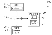
- a transport system having the following configuration. That is, the transport system includes a robot, a sensor, and a determination section.
- the robot has a hand that supports and transports the wafer to an aligner device.
- the sensor detects the position of the wafer while the wafer is supported by the hand before the robot transfers the wafer to the aligner device.
- the determination unit determines positional deviation of the wafer based on the detection value of the sensor.
- the following determination method is provided. That is, in the determination method, the positional deviation of the wafer is determined while the wafer is being transported. Using a robot hand, the wafer is supported and transported to an aligner device. Before the robot transfers the wafer to the aligner device, a sensor is used to detect the position of the edge of the wafer while the wafer is supported by the hand. Positional deviation of the wafer is determined based on the detection value of the sensor.
- the positional displacement of the wafer is detected before the wafer is placed on the aligner, so that problems that may occur in the aligner due to the positional displacement of the wafer can be prevented.
- FIG. 1 is a perspective view of a transport system according to an embodiment of the present application;
- FIG. A block diagram of a transport system. 4 is a flow chart showing a process of determining a positional deviation of a wafer using an aligner sensor;
- FIG. 4 is an explanatory view showing a situation in which a wafer misalignment is determined using an aligner sensor;
- FIG. 4 is an explanatory diagram showing a method of correcting the target position of the wafer based on the positional deviation;
- FIG. 4 is an explanatory view showing a situation in which the positional deviation of the wafer is large and is not detected by the aligner sensor;
- 4 is a flow chart showing a process of determining a positional deviation of a wafer using a protrusion detection sensor;
- FIG. 10 is an explanatory view showing a situation in which a protrusion detection sensor is used to determine a positional deviation of a wafer;
- FIG. 1 is a perspective view showing the configuration of the transport system 100. As shown in FIG. 1
- a transfer system 100 shown in FIG. 1 is a system that transfers a wafer 1, which is an object to be transferred, in a work space such as a clean room.
- the transport system 100 includes a robot 10 and a controller (determination unit) 19 .
- the robot 10 of this embodiment takes out the wafer 1 accommodated in the accommodation unit 30 and conveys it to the aligner device 20 .
- the robot 10 is realized by a SCARA type horizontal articulated robot.
- SCARA is an abbreviation for Selective Compliance Assembly Robot Arm.
- the wafer 1 carried by the robot 10 is a semiconductor wafer.
- the wafer 1 is formed in a circular thin plate shape.
- the wafer 1 may be a glass wafer instead of a semiconductor wafer.
- the robot 10 includes a base 11, an arm 12, and a hand 13, as shown in FIG.
- the base 11 is fixed to the floor of the factory or the like. However, it is not limited to this, and the base 11 may be fixed to, for example, appropriate processing equipment.
- the arm 12 is attached to the base 11 via an elevating shaft 14 that is vertically movable. Arm 12 is rotatable with respect to elevation shaft 14 .
- the arm 12 is a horizontal articulated arm.
- the arm 12 includes a first arm 12a and a second arm 12b.
- the first arm 12a is an elongated member that extends horizontally and linearly. One end in the longitudinal direction of the first arm 12 a is attached to the upper end of the elevation shaft 14 .
- the first arm 12a is rotatably supported about the axis (vertical axis) of the lifting shaft 14. As shown in FIG. A second arm 12b is attached to the other end in the longitudinal direction of the first arm 12a.
- the second arm 12b is an elongated member extending horizontally and linearly. One longitudinal end of the second arm 12b is attached to the tip of the first arm 12a.
- the second arm 12b is rotatably supported about an axis (vertical axis) parallel to the elevation shaft 14. As shown in FIG.
- the hand 13 is connected to the second arm 12b.
- the hand 13 is attached to the tip of the second arm 12b.
- the hand 13 is rotatably supported about an axis (vertical axis) parallel to the elevation shaft 14 .
- the hand 13 is rotationally driven by an appropriate actuator (not shown).
- This actuator is, for example, an electric motor.
- the hand 13 of this embodiment is a passive grip type hand having a branched structure.
- the passive grip type is a configuration in which the wafer 1 placed on the hand 13 is not fixed.
- the tip portion of the hand 13 is branched into two, and the wafer 1 is placed on the part including the branch.
- the hand 13 is not limited to the edge grip type.
- the hand 13 may be of a suction type.
- the suction type is a configuration (for example, a Bernoulli chuck) that transfers the wafer 1 by suctioning the surface of the wafer 1 with a negative pressure.
- the hand 13 may be of the edge grip type.
- the edge grip type is a configuration in which a plurality of guides provided on the hand 13 are used to sandwich and hold the wafer 1 .
- one hand 13 is provided on the arm 12.
- the arm 12 may be provided with two or more hands 13 .
- two hands 13 are provided at the tip of the second arm 12b of the arm 12 .
- the two hands 13 are independently rotatable around the vertical axis.
- the robot 10 can carry, for example, two wafers 1 at the same time.
- the elevation shaft 14, the first arm 12a and the second arm 12b are each driven by an actuator 15 shown in the block diagram of FIG.
- Actuator 15 is, for example, an electric motor.
- Arm joints positioned between the elevation shaft 14 and the first arm 12a, between the first arm 12a and the second arm 12b, and between the second arm 12b and the hand 13 include the first arm 12a, Encoders (not shown) for detecting the rotational positions of the second arm 12b and the hand 13 are attached. An encoder is also provided at an appropriate position on the robot 10 to detect a change in the position of the first arm 12a in the height direction (that is, the amount of elevation of the elevation shaft 14).
- the controller 19 includes an arithmetic device such as a CPU, and a storage device such as an HDD, SSD, or flash memory.
- the computing device controls the robot 10 by executing programs stored in the storage device. Specifically, the controller 19 transmits a command value to the actuator 15 based on pre-registered work details, encoder detection results, and the like. Thereby, the robot 10 carries out the transfer work of the wafer 1 .
- the controller 19 also controls the aligner device 20 (details will be described later).
- the controller 19 controls the robot 10 and the aligner device 20 .
- the controller that controls the aligner device 20 and the controller that controls the robot 10 may be separate.
- the aligner device 20 performs alignment by acquiring and adjusting the rotational phase of the wafer 1 .
- the rotational phase is the orientation of the wafer 1 that changes as the wafer 1 rotates.
- a notch 1 a is formed in the outer periphery of the wafer 1 . Notch 1a indicates the crystal orientation of the semiconductor. If an orientation flat is formed on the wafer 1 instead of the notch 1a, the aligner device 20 may be configured to detect the orientation flat.
- the aligner device 20 includes a turntable 21 , a motor 22 , a mounting member 23 and an aligner sensor 24 .
- the turntable 21 is disk-shaped and arranged so as to face the vertical direction.
- the wafer 1 is placed on the turntable 21 by the robot 10 .
- the shape of the turntable 21 is not limited to a disc.
- the turntable 21 rotates about the vertical direction as the center of rotation when the driving force of the motor 22 is transmitted.
- the mounting member 23 is fixed to an appropriate position in the factory, such as a member that supports the turntable 21 of the aligner device 20, a member that supports the housing section 30, or the floor of the factory. A part of the aligner sensor 24 is attached to the attachment member 23 .
- the aligner sensor 24 is a line sensor and includes a light projecting section 24a and a light receiving section 24b.
- the aligner sensor 24 of this embodiment is a transmissive light amount detection sensor. Therefore, the light projecting part 24a and the light receiving part 24b are arranged with a space therebetween in the vertical direction (thickness direction of the wafer 1) so as to sandwich the wafer 1 therebetween.
- the light projecting part 24a is on the lower side, but the light projecting part 24a may be on the upper side.
- the light projecting section 24a emits inspection light toward the light receiving section 24b.
- the light receiving portion 24b receives the inspection light partly blocked by the wafer 1.
- FIG. The light receiving unit 24b transmits to the controller 19 a current signal (or a voltage signal obtained by converting the current signal) according to the amount of the received inspection light.
- the controller 19 acquires the rotation phase of the notch 1a of the wafer 1 placed on the turntable 21 based on the current signal output by the aligner sensor 24 (light receiving portion 24b) and the rotation phase of the turntable 21. do.
- the aligner sensor 24 adjusts the rotational phase of the wafer 1 by rotating the wafer 1 (turntable 21) so that the notch 1a faces a predetermined direction under the control of the controller 19.
- the aligner sensor 24 is not limited to the light amount detection sensor, and may be a different sensor.
- a CCD (Charge Coupled Device) sensor can be used as the aligner sensor 24 .
- the CCD sensor detects the edge position of the wafer 1 and transmits it to the controller 19 .
- the edge of the wafer 1 is the radial end of the wafer 1 and its vicinity.
- the controller 19 can obtain the rotation phase of the notch 1a of the wafer 1 placed on the turntable 21, as in the case of using the light amount detection sensor as the aligner sensor 24.
- the storage unit 30 is a container that stores a plurality of wafers 1 arranged in the thickness direction.
- a housing space for housing the wafer 1 is formed in the housing portion 30 .
- a plurality of wafer support portions for placing the edge of the wafer 1 are formed in the accommodation portion 30 .
- the storage unit 30 may be a transportable container, or may be a shelf fixed to the floor surface or the like.
- a protrusion detection sensor 31 is attached to the housing portion 30 .
- the protrusion detection sensor 31 is a sensor that detects whether the wafer 1 accommodated in the accommodation portion 30 protrudes from the accommodation space (whether the wafer 1 is positioned outside the accommodation space).
- the protrusion detection sensor 31 includes a light projecting portion 31a and a light receiving portion 31b.
- the light projecting part 31a and the light receiving part 31b are arranged with a space therebetween in the vertical direction (the direction in which the wafers 1 are arranged).
- the light projecting section 31a emits inspection light toward the light receiving section 31b. When the wafer 1 is not positioned between the light projecting portion 31a and the light receiving portion 31b, the light receiving portion 31b receives the inspection light.
- the light receiving portion 31b When the wafer 1 is positioned between the light projecting portion 31a and the light receiving portion 31b, the light receiving portion 31b does not receive the inspection light.
- the light receiving unit 31b transmits to the controller 19 a signal indicating whether or not the inspection light has been received.
- the robot 10 takes out and supports the wafer 1 by positioning the hand 13 below the wafer 1 stored in the storage unit 30 and raising the hand 13 .
- the position of the wafer 1 accommodated in the accommodation unit 30 is displaced, or if the position of the wafer 1 is displaced when the hand 13 takes out the wafer 1, the position of the wafer 1 supported by the hand 13 is changed. There may be deviations. In this case, there is a possibility that the wafer 1 will not be placed in the center of the turntable 21 and the alignment will not be properly performed. Alternatively, if the positional deviation of the wafer 1 is large, the wafer 1 may collide with the mounting member 23 .
- the position of the wafer 1 is detected while the wafer 1 is supported by the hand 13 before the robot 10 delivers the wafer 1 to the aligner device 20 .
- the position of the wafer 1 can be detected using the aligner sensor 24 or protrusion detection sensor 31 . A specific description will be given below.
- the controller 19 uses the hand 13 to take out the wafer 1 stored in the storage unit 30 (S101). Next, the controller 19 moves the wafer 1 to the detection area 91 of the aligner sensor 24 by moving the arm 12 while maintaining the state where the hand 13 supports the wafer 1 (S102). As shown in FIG. 4 , the detection area 91 of the aligner sensor 24 is in the vicinity of the turntable 21 , so the controller 19 brings the center of the hand 13 closer to the center of the turntable 21 .
- the light receiving part 24b of the aligner sensor 24 transmits the above-described current signal to the controller 19 at predetermined time intervals. Therefore, when the edge of the wafer 1 enters the detection area 91, the edge of the wafer 1 is detected multiple times while the wafer 1 is moving.
- the controller 19 determines whether or not the aligner sensor 24 has detected the wafer 1 (S103). 1 is calculated (S104).
- the positional deviation of the wafer 1 is the current position of the wafer 1 with respect to the prescribed position of the wafer 1 (the position determined in the teaching of the robot 10, the position of the wafer 1 when the center of the hand 13 and the center of the wafer 1 coincide). is the difference. Specifically, the positional deviation is indicated by coordinate values in a plane coordinate system. There are various methods for calculating the positional deviation of the wafer 1. For example, the following method can be used.
- the wafer 1 when the wafer 1 is at a specified position, it is estimated how the detection value of the aligner sensor 24 changes according to the position of the hand 13, and is stored as a reference value. Then, the reference value and the detected value actually detected by the aligner sensor 24 are compared according to the position of the hand 13 .
- the position of the wafer 1 is shifted in the front-rear direction (vertical direction in FIG. 4)
- the timing at which the aligner sensor 24 starts detecting the edge of the wafer 1 differs from the reference value. For example, when the position of the wafer 1 is ahead of the specified position, the aligner sensor 24 detects the edge of the wafer 1 at a timing earlier than the reference value.
- the positional deviation of the wafer 1 in the front-rear direction can be calculated. Further, when the position of the wafer 1 is shifted in the horizontal direction (horizontal direction in FIG. 4), the minimum detection value of the aligner sensor 24 is different from the reference value. For example, when the position of the wafer 1 is to the left of the specified position, the area where the wafer 1 blocks the detection area 91 is small, so the minimum detection value of the aligner sensor 24 is large. Therefore, the positional deviation of the wafer 1 in the horizontal direction can be calculated based on the minimum detected value of the aligner sensor 24 . As described above, the controller 19 can calculate the positional deviation of the wafer 1 in the front, rear, left, and right directions.
- the position of the edge of the wafer 1 can be specifically specified based on the detection result of the edge of the wafer 1 by the CCD sensor. Therefore, even if a CCD sensor is used as the aligner sensor 24 , the positional deviation of the wafer 1 can be calculated based on the detection value of the aligner sensor 24 .
- the controller 19 determines whether or not the positional deviation of the wafer 1 calculated in step S104 is equal to or less than the allowable value (S105).
- the allowable value is set within a range in which the wafer 1 does not collide with the mounting member 23 or the like when the hand 13 places the wafer 1 on the turntable 21 .
- Allowable values may be set separately for the front-rear direction and the left-right direction. Alternatively, a tolerance may be set for the distance from the wafer 1 at the prescribed position to the actual wafer 1 .
- the controller 19 corrects the target position based on the positional deviation and places the wafer 1 on the turntable 21 of the aligner device 20 (S106). Specifically, as shown in FIG. 5, the wafer 1 is placed at the corrected target position, which is moved in the direction opposite to the positional deviation and by the same length so as to cancel the influence of the positional deviation. After that, the controller 19 repeats the processes after step S101.
- the controller 19 corrects the holding position of the wafer 1 by the hand 13 (S109). Specifically, the holding position of the wafer 1 by the hand 13 is corrected by once placing the wafer 1 in another place (for example, the storage unit 30) and then taking out the wafer 1 again. Instead of correcting the holding position of the wafer 1, an error may be notified and the work may be stopped.
- the controller 19 performs the following processing. That is, when it is determined in step S103 that the aligner sensor 24 does not detect the wafer 1, the controller 19 moves the hand 13 to move the wafer 1 (S107), and determines whether the hand 13 has reached the limit position. is determined (S108).
- the limit position is a position where collision between the wafer 1 and the mounting member 23 cannot occur. In other words, if the position of the hand 13 moves forward beyond the limit position, the wafer 1 may come into contact with the mounting member 23 .
- the controller 19 determines that the positional deviation of the wafer 1 exceeds the allowable value, and corrects the holding position of the wafer 1 as described above (S109). If there is a possibility that the wafer 1 will collide with an object other than the mounting member 23, the limit position is set further considering the position of the object.
- the protrusion detection sensor 31 is used to detect the position of the wafer 1. A process for transferring the wafer 1 will be described.
- the controller 19 uses the hand 13 to take out the wafer 1 stored in the storage unit 30 (S201). Next, the controller 19 moves the hand 13 in a direction (first direction, rearward) away from the accommodating section 30 to a position where the protrusion detection sensor 31 detects the edge of the wafer 1 (S202). Specifically, immediately after the hand 13 is moved in the first direction, the detection area 92 of the protrusion detection sensor 31 overlaps the wafer 1 (upper left in FIG. 8). By moving the hand 13 in the first direction, the detection area 92 does not overlap the wafer 1 (upper right in FIG. 8).
- the protrusion detection sensor 31 can detect the edge of the wafer 1 based on the switch from the state in which the protrusion detection sensor 31 detects the wafer 1 to the state in which the protrusion detection sensor 31 does not detect the wafer 1 .
- the position of the hand 13 at this time is called the first position.
- the controller 19 moves the hand 13 by a predetermined length in a direction different from the first direction (a second direction, a direction orthogonal to the first direction, specifically either left or right) (S203, FIG. 8 upper right to Fig. 8 lower left).
- the controller 19 moves the hand 13 in the third direction (forward, opposite to the first direction) to approach the container 30 to the position where the protrusion detection sensor 31 detects the edge of the wafer 1 again (S204, FIG. 8 bottom left to bottom right).
- the position of the hand 13 when the protrusion detection sensor 31 detects the edge of the wafer 1 again is called the second position. It is also possible to calculate the positional deviation of the wafer 1 by the above-described method using another sensor arranged outside the housing section 30 .
- the controller 19 calculates the positional deviation of the wafer 1 based on the positions (two positions in this embodiment) of the hand 13 when the protrusion detection sensor 31 detects the edge of the wafer 1 (S205). Specifically, when the wafer 1 is at a specified position, the first position and the second position are stored in advance as a first reference position and a second reference position. By comparing the first reference position with the actual first position and the second reference position with the actual second position, the positional deviation of the wafer 1 can be calculated.
- the subsequent processing is the same as when using the aligner sensor 24 as the sensor. That is, when it is determined that the positional deviation is equal to or less than the allowable value (S206), the target position is corrected based on the positional deviation and the wafer 1 is placed on the turntable 21 (S207). Further, when it is determined that the positional deviation exceeds the allowable value (S206), the holding position of the wafer 1 by the hand 13 is corrected (S208).
- the transport system 100 of this embodiment includes the robot 10, sensors (aligner sensor 24, protrusion detection sensor 31), and controller 19.
- the robot 10 has a hand 13 that supports the wafer 1 and conveys it to the aligner device 20 .
- the sensor detects the position of the wafer 1 while the wafer 1 is supported by the hand 13 before the robot 10 delivers the wafer 1 to the aligner device 20 .
- the controller 19 determines the positional deviation of the wafer 1 based on the detection value of the sensor.
- the positional displacement of the wafer 1 is detected before the wafer 1 is placed on the aligner device 20, so problems that may occur in the aligner device 20 due to the positional displacement of the wafer 1 can be prevented.
- the controller 19 determines whether the positional deviation of the wafer 1 is equal to or less than the allowable value based on the detection value of the sensor. When the controller 19 determines that the positional deviation of the wafer 1 is equal to or less than the allowable value, the robot 10 continues to transfer the wafer 1 to the aligner device 20 .
- the robot 10 when the controller 19 determines that the positional deviation of the wafer 1 is equal to or less than the allowable value, the robot 10 corrects the target position for transporting the wafer 1 based on the positional deviation of the wafer 1. Place the wafer 1 at the corrected target position.
- the robot 10 suspends transport of the wafer 1 to the aligner device 20 .
- the sensor is the aligner sensor 24 that detects the wafer 1 when the aligner device 20 aligns the wafer 1 .
- positional deviation of the wafer 1 can be detected before the wafer 1 is placed on the aligner device 20 without adding a new sensor.
- positional deviation of the wafer 1 can be detected immediately before placing it on the aligner device 20 .
- the aligner sensor 24 is a light amount detection sensor that includes a light projecting section 24a and a light receiving section 24b.
- the light projecting unit 24a emits inspection light.
- the light receiving unit 24b receives the inspection light partly blocked by the wafer 1 and outputs a value corresponding to the amount of light. While the hand 13 is moving the wafer 1, the aligner sensor 24 detects the wafer 1 multiple times.
- the aligner sensor 24 may be configured to receive the light reflected by the wafer 1 from the inspection light with the light receiving section 24b.
- positional deviation of the wafer 1 can be detected using the light amount detection sensor before the wafer 1 is placed on the aligner device 20 . Further, since the aligner sensor 24 detects the wafer 1 multiple times, the positional deviation of the wafer 1 can be detected in detail.
- the aligner sensor 24 may be a CCD sensor that detects the edge position of the wafer 1 .
- the positional deviation of the wafer 1 can be detected using the CCD sensor before the wafer 1 is placed on the aligner device 20 .
- the hand 13 takes out the wafer 1 stored in the storage unit 30 and transports the wafer 1 to the aligner device 20 .
- the sensor is a protrusion detection sensor 31 that detects whether or not the wafer 1 protrudes from the storage space of the storage section 30 .
- the positional deviation of the wafer 1 can be detected before the wafer 1 is placed on the aligner device 20 without adding a new sensor. Further, positional displacement of the wafer 1 can be detected early.
- the senor includes a light projecting portion 31a and a light receiving portion 31b. It is detected whether or not the wafer 1 exists between the portion 31a and the light receiving portion 31b.
- the controller 19 obtains a plurality of positions of the hand 13 when the wafer 1 detects the edge of the wafer 1 , and determines positional deviation of the wafer 1 based on the plurality of positions of the hand 13 .
- the positional deviation of the wafer 1 can be detected before the wafer 1 is placed on the aligner device 20 using a sensor that determines whether or not an object exists between the light projecting section 31a and the light receiving section 31b.
- the hand 13 is of a passive grip type in which the wafer 1 is placed on the hand 13 and transferred without holding the edge.
- the hand 13 may be of a suction type that transfers the wafer 1 by suctioning the surface of the wafer 1 with a negative pressure.
- the passive grip type or suction type hand 13 has a simple configuration, but is characterized in that the wafer 1 is likely to be displaced. By providing the configuration of the present embodiment, it is possible to improve the tendency of the wafer 1 to be misaligned.
- an optical sensor was used as an example of the protrusion detection sensor 31, but it is not limited to an optical sensor, and may be an image sensor, for example.
- a configuration in which the base 11 is installed on the floor surface of the factory a configuration in which the base 11 is installed on the ceiling surface (ceiling type) may be used.
- a processor is considered a processing circuit or circuit because it includes transistors and other circuits.
- a circuit, unit, or means is hardware that performs or is programmed to perform the recited functions.
- the hardware may be the hardware disclosed herein, or other known hardware programmed or configured to perform the functions recited.
- a circuit, means or unit is a combination of hardware and software, where the hardware is a processor which is considered a type of circuit, the software being used to configure the hardware and/or the processor.
Priority Applications (3)
| Application Number | Priority Date | Filing Date | Title |
|---|---|---|---|
| CN202280040528.4A CN117836923A (zh) | 2021-06-10 | 2022-06-02 | 运送系统以及判定方法 |
| JP2023527825A JPWO2022259948A1 (zh) | 2021-06-10 | 2022-06-02 | |
| KR1020247001040A KR20240041909A (ko) | 2021-06-10 | 2022-06-02 | 반송 시스템 및 판정 방법 |
Applications Claiming Priority (2)
| Application Number | Priority Date | Filing Date | Title |
|---|---|---|---|
| US17/343,765 | 2021-06-10 | ||
| US17/343,765 US20220399218A1 (en) | 2021-06-10 | 2021-06-10 | Transport system and determination method |
Publications (1)
| Publication Number | Publication Date |
|---|---|
| WO2022259948A1 true WO2022259948A1 (ja) | 2022-12-15 |
Family
ID=84390496
Family Applications (1)
| Application Number | Title | Priority Date | Filing Date |
|---|---|---|---|
| PCT/JP2022/022446 WO2022259948A1 (ja) | 2021-06-10 | 2022-06-02 | 搬送システム及び判定方法 |
Country Status (6)
| Country | Link |
|---|---|
| US (1) | US20220399218A1 (zh) |
| JP (1) | JPWO2022259948A1 (zh) |
| KR (1) | KR20240041909A (zh) |
| CN (1) | CN117836923A (zh) |
| TW (1) | TWI822103B (zh) |
| WO (1) | WO2022259948A1 (zh) |
Citations (6)
| Publication number | Priority date | Publication date | Assignee | Title |
|---|---|---|---|---|
| JPH0529441A (ja) * | 1991-07-23 | 1993-02-05 | Oki Electric Ind Co Ltd | ウエハー位置およびオリエンテーシヨンフラツト方向検出方法 |
| JP2008053552A (ja) * | 2006-08-25 | 2008-03-06 | Tokyo Electron Ltd | ウェハ搬送装置、ウェハ搬送方法及び記憶媒体 |
| JP2009054933A (ja) * | 2007-08-29 | 2009-03-12 | Ryusyo Industrial Co Ltd | ウエハ搬送システム |
| JP2011108958A (ja) * | 2009-11-20 | 2011-06-02 | Hitachi High-Tech Control Systems Corp | 半導体ウェーハ搬送装置及びこれを用いた搬送方法 |
| JP2016134526A (ja) * | 2015-01-20 | 2016-07-25 | リンテック株式会社 | 移載装置および移載方法 |
| WO2020226024A1 (ja) * | 2019-05-09 | 2020-11-12 | 川崎重工業株式会社 | 基板搬送ロボット及び基板搬送方法 |
Family Cites Families (12)
| Publication number | Priority date | Publication date | Assignee | Title |
|---|---|---|---|---|
| US3808395A (en) * | 1973-05-15 | 1974-04-30 | Gen Electric | Method of metallurgically joining a beryllium-base part and a copper-base part |
| KR100772843B1 (ko) * | 2006-02-13 | 2007-11-02 | 삼성전자주식회사 | 웨이퍼 얼라인 장치 및 방법 |
| US8600150B2 (en) * | 2006-02-13 | 2013-12-03 | Samsung Electronics Co., Ltd. | Wafer aligning apparatus and related method |
| JP5058836B2 (ja) * | 2007-05-08 | 2012-10-24 | 東京エレクトロン株式会社 | 処理装置、処理方法、被処理体の認識方法および記憶媒体 |
| JP5324231B2 (ja) * | 2009-01-08 | 2013-10-23 | 日東電工株式会社 | 半導体ウエハのアライメント装置 |
| JP5557516B2 (ja) * | 2009-12-09 | 2014-07-23 | 株式会社日立ハイテクノロジーズ | 真空処理装置 |
| JP5600703B2 (ja) | 2012-03-30 | 2014-10-01 | 東京エレクトロン株式会社 | 搬送装置及び搬送方法 |
| JP6339909B2 (ja) * | 2014-09-17 | 2018-06-06 | 株式会社Screenホールディングス | 基板処理装置および基板処理方法 |
| KR101817209B1 (ko) * | 2016-06-24 | 2018-02-22 | 세메스 주식회사 | 기판 처리 장치 및 방법 |
| JP7008573B2 (ja) * | 2018-05-16 | 2022-01-25 | 東京エレクトロン株式会社 | 搬送方法および搬送装置 |
| WO2021245956A1 (ja) * | 2020-06-05 | 2021-12-09 | ローツェ株式会社 | ウエハ搬送装置、およびウエハ搬送方法 |
| KR102624577B1 (ko) * | 2020-10-28 | 2024-01-15 | 세메스 주식회사 | 기판 처리 장치 및 기판 처리 방법 |
-
2021
- 2021-06-10 US US17/343,765 patent/US20220399218A1/en active Pending
-
2022
- 2022-06-02 CN CN202280040528.4A patent/CN117836923A/zh active Pending
- 2022-06-02 WO PCT/JP2022/022446 patent/WO2022259948A1/ja active Application Filing
- 2022-06-02 KR KR1020247001040A patent/KR20240041909A/ko unknown
- 2022-06-02 JP JP2023527825A patent/JPWO2022259948A1/ja active Pending
- 2022-06-10 TW TW111121547A patent/TWI822103B/zh active
Patent Citations (6)
| Publication number | Priority date | Publication date | Assignee | Title |
|---|---|---|---|---|
| JPH0529441A (ja) * | 1991-07-23 | 1993-02-05 | Oki Electric Ind Co Ltd | ウエハー位置およびオリエンテーシヨンフラツト方向検出方法 |
| JP2008053552A (ja) * | 2006-08-25 | 2008-03-06 | Tokyo Electron Ltd | ウェハ搬送装置、ウェハ搬送方法及び記憶媒体 |
| JP2009054933A (ja) * | 2007-08-29 | 2009-03-12 | Ryusyo Industrial Co Ltd | ウエハ搬送システム |
| JP2011108958A (ja) * | 2009-11-20 | 2011-06-02 | Hitachi High-Tech Control Systems Corp | 半導体ウェーハ搬送装置及びこれを用いた搬送方法 |
| JP2016134526A (ja) * | 2015-01-20 | 2016-07-25 | リンテック株式会社 | 移載装置および移載方法 |
| WO2020226024A1 (ja) * | 2019-05-09 | 2020-11-12 | 川崎重工業株式会社 | 基板搬送ロボット及び基板搬送方法 |
Also Published As
| Publication number | Publication date |
|---|---|
| TW202306014A (zh) | 2023-02-01 |
| TWI822103B (zh) | 2023-11-11 |
| JPWO2022259948A1 (zh) | 2022-12-15 |
| US20220399218A1 (en) | 2022-12-15 |
| KR20240041909A (ko) | 2024-04-01 |
| CN117836923A (zh) | 2024-04-05 |
Similar Documents
| Publication | Publication Date | Title |
|---|---|---|
| JP4402811B2 (ja) | 被処理体の搬送システムおよび被処理体の位置ずれ量の検出方法 | |
| CN107530877B (zh) | 机器人的示教方法及机器人 | |
| KR101817209B1 (ko) | 기판 처리 장치 및 방법 | |
| US10468284B2 (en) | Substrate processing apparatus and substrate processing method | |
| US8989901B2 (en) | Transfer system | |
| US20180218935A1 (en) | Substrate transport device, detection position calibration method and substrate processing apparatus | |
| JP2008173744A (ja) | 搬送システムの搬送位置合わせ方法 | |
| US9908236B2 (en) | Transfer system and transfer method | |
| JP5185054B2 (ja) | 基板搬送方法、制御プログラム及び記憶媒体 | |
| TW201102236A (en) | Robot, and auto-zeroing method | |
| WO2004043653A1 (ja) | 搬送機構の基準位置の補正装置および補正方法 | |
| JP2013149902A (ja) | ウエハ搬送装置 | |
| JP2009081267A (ja) | 基板搬送位置の位置合わせ方法、基板処理システムおよびコンピュータ読み取り可能な記憶媒体 | |
| JPWO2005004227A1 (ja) | 薄板状物の変位量検出方法及び変位量修正方法 | |
| JPH106262A (ja) | ロボットの教示方法及びその装置 | |
| JP2011108958A (ja) | 半導体ウェーハ搬送装置及びこれを用いた搬送方法 | |
| WO2022259948A1 (ja) | 搬送システム及び判定方法 | |
| CN115039214A (zh) | 基板搬运装置以及基板位置偏移测定方法 | |
| JP2006185960A (ja) | 基板処理装置及びその搬送位置合わせ方法 | |
| TWI823237B (zh) | 對準裝置及對準方法 | |
| KR102462619B1 (ko) | 기판 처리 장치, 기판 처리 장치의 운전 방법 및 기억 매체 | |
| KR20110056841A (ko) | 웨이퍼 정렬장치 및 이를 포함하는 로드락 챔버 | |
| JP7129788B2 (ja) | 産業用ロボットの補正値算出方法 | |
| JP2009184069A (ja) | ウエハ搬送装置及びその調整方法 | |
| US20240058952A1 (en) | Controller for substrate transfer robot and control method for joint motor |
Legal Events
| Date | Code | Title | Description |
|---|---|---|---|
| 121 | Ep: the epo has been informed by wipo that ep was designated in this application |
Ref document number: 22820130 Country of ref document: EP Kind code of ref document: A1 |
|
| WWE | Wipo information: entry into national phase |
Ref document number: 2023527825 Country of ref document: JP |
|
| WWE | Wipo information: entry into national phase |
Ref document number: 1020247001040 Country of ref document: KR |
|
| NENP | Non-entry into the national phase |
Ref country code: DE |