WO2022259948A1 - 搬送システム及び判定方法 - Google Patents
搬送システム及び判定方法 Download PDFInfo
- Publication number
- WO2022259948A1 WO2022259948A1 PCT/JP2022/022446 JP2022022446W WO2022259948A1 WO 2022259948 A1 WO2022259948 A1 WO 2022259948A1 JP 2022022446 W JP2022022446 W JP 2022022446W WO 2022259948 A1 WO2022259948 A1 WO 2022259948A1
- Authority
- WO
- WIPO (PCT)
- Prior art keywords
- wafer
- sensor
- aligner
- hand
- positional deviation
- Prior art date
Links
- 238000000034 method Methods 0.000 title claims description 17
- 238000001514 detection method Methods 0.000 claims abstract description 49
- 235000012431 wafers Nutrition 0.000 claims description 249
- 230000032258 transport Effects 0.000 claims description 34
- 238000007689 inspection Methods 0.000 claims description 15
- 230000004308 accommodation Effects 0.000 claims description 7
- 239000000758 substrate Substances 0.000 description 12
- 238000006073 displacement reaction Methods 0.000 description 7
- 238000010586 diagram Methods 0.000 description 3
- 239000004065 semiconductor Substances 0.000 description 3
- 230000006870 function Effects 0.000 description 2
- 230000003287 optical effect Effects 0.000 description 2
- 239000013078 crystal Substances 0.000 description 1
- 230000000694 effects Effects 0.000 description 1
- 230000003028 elevating effect Effects 0.000 description 1
- 239000011521 glass Substances 0.000 description 1
Images


Classifications
-
- H—ELECTRICITY
- H01—ELECTRIC ELEMENTS
- H01L—SEMICONDUCTOR DEVICES NOT COVERED BY CLASS H10
- H01L21/00—Processes or apparatus adapted for the manufacture or treatment of semiconductor or solid state devices or of parts thereof
- H01L21/67—Apparatus specially adapted for handling semiconductor or electric solid state devices during manufacture or treatment thereof; Apparatus specially adapted for handling wafers during manufacture or treatment of semiconductor or electric solid state devices or components ; Apparatus not specifically provided for elsewhere
- H01L21/67005—Apparatus not specifically provided for elsewhere
- H01L21/67242—Apparatus for monitoring, sorting or marking
- H01L21/67259—Position monitoring, e.g. misposition detection or presence detection
- H01L21/67265—Position monitoring, e.g. misposition detection or presence detection of substrates stored in a container, a magazine, a carrier, a boat or the like
-
- H—ELECTRICITY
- H01—ELECTRIC ELEMENTS
- H01L—SEMICONDUCTOR DEVICES NOT COVERED BY CLASS H10
- H01L21/00—Processes or apparatus adapted for the manufacture or treatment of semiconductor or solid state devices or of parts thereof
- H01L21/67—Apparatus specially adapted for handling semiconductor or electric solid state devices during manufacture or treatment thereof; Apparatus specially adapted for handling wafers during manufacture or treatment of semiconductor or electric solid state devices or components ; Apparatus not specifically provided for elsewhere
- H01L21/68—Apparatus specially adapted for handling semiconductor or electric solid state devices during manufacture or treatment thereof; Apparatus specially adapted for handling wafers during manufacture or treatment of semiconductor or electric solid state devices or components ; Apparatus not specifically provided for elsewhere for positioning, orientation or alignment
- H01L21/681—Apparatus specially adapted for handling semiconductor or electric solid state devices during manufacture or treatment thereof; Apparatus specially adapted for handling wafers during manufacture or treatment of semiconductor or electric solid state devices or components ; Apparatus not specifically provided for elsewhere for positioning, orientation or alignment using optical controlling means
-
- H—ELECTRICITY
- H01—ELECTRIC ELEMENTS
- H01L—SEMICONDUCTOR DEVICES NOT COVERED BY CLASS H10
- H01L21/00—Processes or apparatus adapted for the manufacture or treatment of semiconductor or solid state devices or of parts thereof
- H01L21/67—Apparatus specially adapted for handling semiconductor or electric solid state devices during manufacture or treatment thereof; Apparatus specially adapted for handling wafers during manufacture or treatment of semiconductor or electric solid state devices or components ; Apparatus not specifically provided for elsewhere
- H01L21/677—Apparatus specially adapted for handling semiconductor or electric solid state devices during manufacture or treatment thereof; Apparatus specially adapted for handling wafers during manufacture or treatment of semiconductor or electric solid state devices or components ; Apparatus not specifically provided for elsewhere for conveying, e.g. between different workstations
- H01L21/67763—Apparatus specially adapted for handling semiconductor or electric solid state devices during manufacture or treatment thereof; Apparatus specially adapted for handling wafers during manufacture or treatment of semiconductor or electric solid state devices or components ; Apparatus not specifically provided for elsewhere for conveying, e.g. between different workstations the wafers being stored in a carrier, involving loading and unloading
- H01L21/67766—Mechanical parts of transfer devices
-
- H—ELECTRICITY
- H01—ELECTRIC ELEMENTS
- H01L—SEMICONDUCTOR DEVICES NOT COVERED BY CLASS H10
- H01L21/00—Processes or apparatus adapted for the manufacture or treatment of semiconductor or solid state devices or of parts thereof
- H01L21/67—Apparatus specially adapted for handling semiconductor or electric solid state devices during manufacture or treatment thereof; Apparatus specially adapted for handling wafers during manufacture or treatment of semiconductor or electric solid state devices or components ; Apparatus not specifically provided for elsewhere
- H01L21/677—Apparatus specially adapted for handling semiconductor or electric solid state devices during manufacture or treatment thereof; Apparatus specially adapted for handling wafers during manufacture or treatment of semiconductor or electric solid state devices or components ; Apparatus not specifically provided for elsewhere for conveying, e.g. between different workstations
- H01L21/67763—Apparatus specially adapted for handling semiconductor or electric solid state devices during manufacture or treatment thereof; Apparatus specially adapted for handling wafers during manufacture or treatment of semiconductor or electric solid state devices or components ; Apparatus not specifically provided for elsewhere for conveying, e.g. between different workstations the wafers being stored in a carrier, involving loading and unloading
- H01L21/67769—Storage means
-
- H—ELECTRICITY
- H01—ELECTRIC ELEMENTS
- H01L—SEMICONDUCTOR DEVICES NOT COVERED BY CLASS H10
- H01L21/00—Processes or apparatus adapted for the manufacture or treatment of semiconductor or solid state devices or of parts thereof
- H01L21/67—Apparatus specially adapted for handling semiconductor or electric solid state devices during manufacture or treatment thereof; Apparatus specially adapted for handling wafers during manufacture or treatment of semiconductor or electric solid state devices or components ; Apparatus not specifically provided for elsewhere
- H01L21/677—Apparatus specially adapted for handling semiconductor or electric solid state devices during manufacture or treatment thereof; Apparatus specially adapted for handling wafers during manufacture or treatment of semiconductor or electric solid state devices or components ; Apparatus not specifically provided for elsewhere for conveying, e.g. between different workstations
- H01L21/67763—Apparatus specially adapted for handling semiconductor or electric solid state devices during manufacture or treatment thereof; Apparatus specially adapted for handling wafers during manufacture or treatment of semiconductor or electric solid state devices or components ; Apparatus not specifically provided for elsewhere for conveying, e.g. between different workstations the wafers being stored in a carrier, involving loading and unloading
- H01L21/67778—Apparatus specially adapted for handling semiconductor or electric solid state devices during manufacture or treatment thereof; Apparatus specially adapted for handling wafers during manufacture or treatment of semiconductor or electric solid state devices or components ; Apparatus not specifically provided for elsewhere for conveying, e.g. between different workstations the wafers being stored in a carrier, involving loading and unloading involving loading and unloading of wafers
-
- H—ELECTRICITY
- H01—ELECTRIC ELEMENTS
- H01L—SEMICONDUCTOR DEVICES NOT COVERED BY CLASS H10
- H01L21/00—Processes or apparatus adapted for the manufacture or treatment of semiconductor or solid state devices or of parts thereof
- H01L21/67—Apparatus specially adapted for handling semiconductor or electric solid state devices during manufacture or treatment thereof; Apparatus specially adapted for handling wafers during manufacture or treatment of semiconductor or electric solid state devices or components ; Apparatus not specifically provided for elsewhere
- H01L21/683—Apparatus specially adapted for handling semiconductor or electric solid state devices during manufacture or treatment thereof; Apparatus specially adapted for handling wafers during manufacture or treatment of semiconductor or electric solid state devices or components ; Apparatus not specifically provided for elsewhere for supporting or gripping
- H01L21/6838—Apparatus specially adapted for handling semiconductor or electric solid state devices during manufacture or treatment thereof; Apparatus specially adapted for handling wafers during manufacture or treatment of semiconductor or electric solid state devices or components ; Apparatus not specifically provided for elsewhere for supporting or gripping with gripping and holding devices using a vacuum; Bernoulli devices
-
- H—ELECTRICITY
- H01—ELECTRIC ELEMENTS
- H01L—SEMICONDUCTOR DEVICES NOT COVERED BY CLASS H10
- H01L21/00—Processes or apparatus adapted for the manufacture or treatment of semiconductor or solid state devices or of parts thereof
- H01L21/67—Apparatus specially adapted for handling semiconductor or electric solid state devices during manufacture or treatment thereof; Apparatus specially adapted for handling wafers during manufacture or treatment of semiconductor or electric solid state devices or components ; Apparatus not specifically provided for elsewhere
- H01L21/683—Apparatus specially adapted for handling semiconductor or electric solid state devices during manufacture or treatment thereof; Apparatus specially adapted for handling wafers during manufacture or treatment of semiconductor or electric solid state devices or components ; Apparatus not specifically provided for elsewhere for supporting or gripping
- H01L21/687—Apparatus specially adapted for handling semiconductor or electric solid state devices during manufacture or treatment thereof; Apparatus specially adapted for handling wafers during manufacture or treatment of semiconductor or electric solid state devices or components ; Apparatus not specifically provided for elsewhere for supporting or gripping using mechanical means, e.g. chucks, clamps or pinches
- H01L21/68707—Apparatus specially adapted for handling semiconductor or electric solid state devices during manufacture or treatment thereof; Apparatus specially adapted for handling wafers during manufacture or treatment of semiconductor or electric solid state devices or components ; Apparatus not specifically provided for elsewhere for supporting or gripping using mechanical means, e.g. chucks, clamps or pinches the wafers being placed on a robot blade, or gripped by a gripper for conveyance
Definitions
- This application mainly relates to a transfer system that transfers wafers using a robot. More specifically, the present invention relates to a configuration for detecting positional deviation of a wafer during wafer transfer.
- Patent Document 1 Japanese Patent Application Laid-Open No. 2013-2113157 discloses a transfer device that transfers a substrate (wafer).
- the transport device of Patent Literature 1 includes a container, a transport unit, and an alignment unit.
- the transport unit takes out the substrate stored in the storage container and transports it to the alignment unit.
- the alignment unit the position of the substrate placed on the turntable is grasped by placing the substrate on the turntable and rotating it and detecting the outer edge of the substrate with a sensor.
- the present application has been made in view of the above circumstances, and its main object is to provide a transfer system that can prevent problems that may occur in an aligner apparatus due to positional displacement of wafers. .
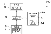
- a transport system having the following configuration. That is, the transport system includes a robot, a sensor, and a determination section.
- the robot has a hand that supports and transports the wafer to an aligner device.
- the sensor detects the position of the wafer while the wafer is supported by the hand before the robot transfers the wafer to the aligner device.
- the determination unit determines positional deviation of the wafer based on the detection value of the sensor.
- the following determination method is provided. That is, in the determination method, the positional deviation of the wafer is determined while the wafer is being transported. Using a robot hand, the wafer is supported and transported to an aligner device. Before the robot transfers the wafer to the aligner device, a sensor is used to detect the position of the edge of the wafer while the wafer is supported by the hand. Positional deviation of the wafer is determined based on the detection value of the sensor.
- the positional displacement of the wafer is detected before the wafer is placed on the aligner, so that problems that may occur in the aligner due to the positional displacement of the wafer can be prevented.
- FIG. 1 is a perspective view of a transport system according to an embodiment of the present application;
- FIG. A block diagram of a transport system. 4 is a flow chart showing a process of determining a positional deviation of a wafer using an aligner sensor;
- FIG. 4 is an explanatory view showing a situation in which a wafer misalignment is determined using an aligner sensor;
- FIG. 4 is an explanatory diagram showing a method of correcting the target position of the wafer based on the positional deviation;
- FIG. 4 is an explanatory view showing a situation in which the positional deviation of the wafer is large and is not detected by the aligner sensor;
- 4 is a flow chart showing a process of determining a positional deviation of a wafer using a protrusion detection sensor;
- FIG. 10 is an explanatory view showing a situation in which a protrusion detection sensor is used to determine a positional deviation of a wafer;
- FIG. 1 is a perspective view showing the configuration of the transport system 100. As shown in FIG. 1
- a transfer system 100 shown in FIG. 1 is a system that transfers a wafer 1, which is an object to be transferred, in a work space such as a clean room.
- the transport system 100 includes a robot 10 and a controller (determination unit) 19 .
- the robot 10 of this embodiment takes out the wafer 1 accommodated in the accommodation unit 30 and conveys it to the aligner device 20 .
- the robot 10 is realized by a SCARA type horizontal articulated robot.
- SCARA is an abbreviation for Selective Compliance Assembly Robot Arm.
- the wafer 1 carried by the robot 10 is a semiconductor wafer.
- the wafer 1 is formed in a circular thin plate shape.
- the wafer 1 may be a glass wafer instead of a semiconductor wafer.
- the robot 10 includes a base 11, an arm 12, and a hand 13, as shown in FIG.
- the base 11 is fixed to the floor of the factory or the like. However, it is not limited to this, and the base 11 may be fixed to, for example, appropriate processing equipment.
- the arm 12 is attached to the base 11 via an elevating shaft 14 that is vertically movable. Arm 12 is rotatable with respect to elevation shaft 14 .
- the arm 12 is a horizontal articulated arm.
- the arm 12 includes a first arm 12a and a second arm 12b.
- the first arm 12a is an elongated member that extends horizontally and linearly. One end in the longitudinal direction of the first arm 12 a is attached to the upper end of the elevation shaft 14 .
- the first arm 12a is rotatably supported about the axis (vertical axis) of the lifting shaft 14. As shown in FIG. A second arm 12b is attached to the other end in the longitudinal direction of the first arm 12a.
- the second arm 12b is an elongated member extending horizontally and linearly. One longitudinal end of the second arm 12b is attached to the tip of the first arm 12a.
- the second arm 12b is rotatably supported about an axis (vertical axis) parallel to the elevation shaft 14. As shown in FIG.
- the hand 13 is connected to the second arm 12b.
- the hand 13 is attached to the tip of the second arm 12b.
- the hand 13 is rotatably supported about an axis (vertical axis) parallel to the elevation shaft 14 .
- the hand 13 is rotationally driven by an appropriate actuator (not shown).
- This actuator is, for example, an electric motor.
- the hand 13 of this embodiment is a passive grip type hand having a branched structure.
- the passive grip type is a configuration in which the wafer 1 placed on the hand 13 is not fixed.
- the tip portion of the hand 13 is branched into two, and the wafer 1 is placed on the part including the branch.
- the hand 13 is not limited to the edge grip type.
- the hand 13 may be of a suction type.
- the suction type is a configuration (for example, a Bernoulli chuck) that transfers the wafer 1 by suctioning the surface of the wafer 1 with a negative pressure.
- the hand 13 may be of the edge grip type.
- the edge grip type is a configuration in which a plurality of guides provided on the hand 13 are used to sandwich and hold the wafer 1 .
- one hand 13 is provided on the arm 12.
- the arm 12 may be provided with two or more hands 13 .
- two hands 13 are provided at the tip of the second arm 12b of the arm 12 .
- the two hands 13 are independently rotatable around the vertical axis.
- the robot 10 can carry, for example, two wafers 1 at the same time.
- the elevation shaft 14, the first arm 12a and the second arm 12b are each driven by an actuator 15 shown in the block diagram of FIG.
- Actuator 15 is, for example, an electric motor.
- Arm joints positioned between the elevation shaft 14 and the first arm 12a, between the first arm 12a and the second arm 12b, and between the second arm 12b and the hand 13 include the first arm 12a, Encoders (not shown) for detecting the rotational positions of the second arm 12b and the hand 13 are attached. An encoder is also provided at an appropriate position on the robot 10 to detect a change in the position of the first arm 12a in the height direction (that is, the amount of elevation of the elevation shaft 14).
- the controller 19 includes an arithmetic device such as a CPU, and a storage device such as an HDD, SSD, or flash memory.
- the computing device controls the robot 10 by executing programs stored in the storage device. Specifically, the controller 19 transmits a command value to the actuator 15 based on pre-registered work details, encoder detection results, and the like. Thereby, the robot 10 carries out the transfer work of the wafer 1 .
- the controller 19 also controls the aligner device 20 (details will be described later).
- the controller 19 controls the robot 10 and the aligner device 20 .
- the controller that controls the aligner device 20 and the controller that controls the robot 10 may be separate.
- the aligner device 20 performs alignment by acquiring and adjusting the rotational phase of the wafer 1 .
- the rotational phase is the orientation of the wafer 1 that changes as the wafer 1 rotates.
- a notch 1 a is formed in the outer periphery of the wafer 1 . Notch 1a indicates the crystal orientation of the semiconductor. If an orientation flat is formed on the wafer 1 instead of the notch 1a, the aligner device 20 may be configured to detect the orientation flat.
- the aligner device 20 includes a turntable 21 , a motor 22 , a mounting member 23 and an aligner sensor 24 .
- the turntable 21 is disk-shaped and arranged so as to face the vertical direction.
- the wafer 1 is placed on the turntable 21 by the robot 10 .
- the shape of the turntable 21 is not limited to a disc.
- the turntable 21 rotates about the vertical direction as the center of rotation when the driving force of the motor 22 is transmitted.
- the mounting member 23 is fixed to an appropriate position in the factory, such as a member that supports the turntable 21 of the aligner device 20, a member that supports the housing section 30, or the floor of the factory. A part of the aligner sensor 24 is attached to the attachment member 23 .
- the aligner sensor 24 is a line sensor and includes a light projecting section 24a and a light receiving section 24b.
- the aligner sensor 24 of this embodiment is a transmissive light amount detection sensor. Therefore, the light projecting part 24a and the light receiving part 24b are arranged with a space therebetween in the vertical direction (thickness direction of the wafer 1) so as to sandwich the wafer 1 therebetween.
- the light projecting part 24a is on the lower side, but the light projecting part 24a may be on the upper side.
- the light projecting section 24a emits inspection light toward the light receiving section 24b.
- the light receiving portion 24b receives the inspection light partly blocked by the wafer 1.
- FIG. The light receiving unit 24b transmits to the controller 19 a current signal (or a voltage signal obtained by converting the current signal) according to the amount of the received inspection light.
- the controller 19 acquires the rotation phase of the notch 1a of the wafer 1 placed on the turntable 21 based on the current signal output by the aligner sensor 24 (light receiving portion 24b) and the rotation phase of the turntable 21. do.
- the aligner sensor 24 adjusts the rotational phase of the wafer 1 by rotating the wafer 1 (turntable 21) so that the notch 1a faces a predetermined direction under the control of the controller 19.
- the aligner sensor 24 is not limited to the light amount detection sensor, and may be a different sensor.
- a CCD (Charge Coupled Device) sensor can be used as the aligner sensor 24 .
- the CCD sensor detects the edge position of the wafer 1 and transmits it to the controller 19 .
- the edge of the wafer 1 is the radial end of the wafer 1 and its vicinity.
- the controller 19 can obtain the rotation phase of the notch 1a of the wafer 1 placed on the turntable 21, as in the case of using the light amount detection sensor as the aligner sensor 24.
- the storage unit 30 is a container that stores a plurality of wafers 1 arranged in the thickness direction.
- a housing space for housing the wafer 1 is formed in the housing portion 30 .
- a plurality of wafer support portions for placing the edge of the wafer 1 are formed in the accommodation portion 30 .
- the storage unit 30 may be a transportable container, or may be a shelf fixed to the floor surface or the like.
- a protrusion detection sensor 31 is attached to the housing portion 30 .
- the protrusion detection sensor 31 is a sensor that detects whether the wafer 1 accommodated in the accommodation portion 30 protrudes from the accommodation space (whether the wafer 1 is positioned outside the accommodation space).
- the protrusion detection sensor 31 includes a light projecting portion 31a and a light receiving portion 31b.
- the light projecting part 31a and the light receiving part 31b are arranged with a space therebetween in the vertical direction (the direction in which the wafers 1 are arranged).
- the light projecting section 31a emits inspection light toward the light receiving section 31b. When the wafer 1 is not positioned between the light projecting portion 31a and the light receiving portion 31b, the light receiving portion 31b receives the inspection light.
- the light receiving portion 31b When the wafer 1 is positioned between the light projecting portion 31a and the light receiving portion 31b, the light receiving portion 31b does not receive the inspection light.
- the light receiving unit 31b transmits to the controller 19 a signal indicating whether or not the inspection light has been received.
- the robot 10 takes out and supports the wafer 1 by positioning the hand 13 below the wafer 1 stored in the storage unit 30 and raising the hand 13 .
- the position of the wafer 1 accommodated in the accommodation unit 30 is displaced, or if the position of the wafer 1 is displaced when the hand 13 takes out the wafer 1, the position of the wafer 1 supported by the hand 13 is changed. There may be deviations. In this case, there is a possibility that the wafer 1 will not be placed in the center of the turntable 21 and the alignment will not be properly performed. Alternatively, if the positional deviation of the wafer 1 is large, the wafer 1 may collide with the mounting member 23 .
- the position of the wafer 1 is detected while the wafer 1 is supported by the hand 13 before the robot 10 delivers the wafer 1 to the aligner device 20 .
- the position of the wafer 1 can be detected using the aligner sensor 24 or protrusion detection sensor 31 . A specific description will be given below.
- the controller 19 uses the hand 13 to take out the wafer 1 stored in the storage unit 30 (S101). Next, the controller 19 moves the wafer 1 to the detection area 91 of the aligner sensor 24 by moving the arm 12 while maintaining the state where the hand 13 supports the wafer 1 (S102). As shown in FIG. 4 , the detection area 91 of the aligner sensor 24 is in the vicinity of the turntable 21 , so the controller 19 brings the center of the hand 13 closer to the center of the turntable 21 .
- the light receiving part 24b of the aligner sensor 24 transmits the above-described current signal to the controller 19 at predetermined time intervals. Therefore, when the edge of the wafer 1 enters the detection area 91, the edge of the wafer 1 is detected multiple times while the wafer 1 is moving.
- the controller 19 determines whether or not the aligner sensor 24 has detected the wafer 1 (S103). 1 is calculated (S104).
- the positional deviation of the wafer 1 is the current position of the wafer 1 with respect to the prescribed position of the wafer 1 (the position determined in the teaching of the robot 10, the position of the wafer 1 when the center of the hand 13 and the center of the wafer 1 coincide). is the difference. Specifically, the positional deviation is indicated by coordinate values in a plane coordinate system. There are various methods for calculating the positional deviation of the wafer 1. For example, the following method can be used.
- the wafer 1 when the wafer 1 is at a specified position, it is estimated how the detection value of the aligner sensor 24 changes according to the position of the hand 13, and is stored as a reference value. Then, the reference value and the detected value actually detected by the aligner sensor 24 are compared according to the position of the hand 13 .
- the position of the wafer 1 is shifted in the front-rear direction (vertical direction in FIG. 4)
- the timing at which the aligner sensor 24 starts detecting the edge of the wafer 1 differs from the reference value. For example, when the position of the wafer 1 is ahead of the specified position, the aligner sensor 24 detects the edge of the wafer 1 at a timing earlier than the reference value.
- the positional deviation of the wafer 1 in the front-rear direction can be calculated. Further, when the position of the wafer 1 is shifted in the horizontal direction (horizontal direction in FIG. 4), the minimum detection value of the aligner sensor 24 is different from the reference value. For example, when the position of the wafer 1 is to the left of the specified position, the area where the wafer 1 blocks the detection area 91 is small, so the minimum detection value of the aligner sensor 24 is large. Therefore, the positional deviation of the wafer 1 in the horizontal direction can be calculated based on the minimum detected value of the aligner sensor 24 . As described above, the controller 19 can calculate the positional deviation of the wafer 1 in the front, rear, left, and right directions.
- the position of the edge of the wafer 1 can be specifically specified based on the detection result of the edge of the wafer 1 by the CCD sensor. Therefore, even if a CCD sensor is used as the aligner sensor 24 , the positional deviation of the wafer 1 can be calculated based on the detection value of the aligner sensor 24 .
- the controller 19 determines whether or not the positional deviation of the wafer 1 calculated in step S104 is equal to or less than the allowable value (S105).
- the allowable value is set within a range in which the wafer 1 does not collide with the mounting member 23 or the like when the hand 13 places the wafer 1 on the turntable 21 .
- Allowable values may be set separately for the front-rear direction and the left-right direction. Alternatively, a tolerance may be set for the distance from the wafer 1 at the prescribed position to the actual wafer 1 .
- the controller 19 corrects the target position based on the positional deviation and places the wafer 1 on the turntable 21 of the aligner device 20 (S106). Specifically, as shown in FIG. 5, the wafer 1 is placed at the corrected target position, which is moved in the direction opposite to the positional deviation and by the same length so as to cancel the influence of the positional deviation. After that, the controller 19 repeats the processes after step S101.
- the controller 19 corrects the holding position of the wafer 1 by the hand 13 (S109). Specifically, the holding position of the wafer 1 by the hand 13 is corrected by once placing the wafer 1 in another place (for example, the storage unit 30) and then taking out the wafer 1 again. Instead of correcting the holding position of the wafer 1, an error may be notified and the work may be stopped.
- the controller 19 performs the following processing. That is, when it is determined in step S103 that the aligner sensor 24 does not detect the wafer 1, the controller 19 moves the hand 13 to move the wafer 1 (S107), and determines whether the hand 13 has reached the limit position. is determined (S108).
- the limit position is a position where collision between the wafer 1 and the mounting member 23 cannot occur. In other words, if the position of the hand 13 moves forward beyond the limit position, the wafer 1 may come into contact with the mounting member 23 .
- the controller 19 determines that the positional deviation of the wafer 1 exceeds the allowable value, and corrects the holding position of the wafer 1 as described above (S109). If there is a possibility that the wafer 1 will collide with an object other than the mounting member 23, the limit position is set further considering the position of the object.
- the protrusion detection sensor 31 is used to detect the position of the wafer 1. A process for transferring the wafer 1 will be described.
- the controller 19 uses the hand 13 to take out the wafer 1 stored in the storage unit 30 (S201). Next, the controller 19 moves the hand 13 in a direction (first direction, rearward) away from the accommodating section 30 to a position where the protrusion detection sensor 31 detects the edge of the wafer 1 (S202). Specifically, immediately after the hand 13 is moved in the first direction, the detection area 92 of the protrusion detection sensor 31 overlaps the wafer 1 (upper left in FIG. 8). By moving the hand 13 in the first direction, the detection area 92 does not overlap the wafer 1 (upper right in FIG. 8).
- the protrusion detection sensor 31 can detect the edge of the wafer 1 based on the switch from the state in which the protrusion detection sensor 31 detects the wafer 1 to the state in which the protrusion detection sensor 31 does not detect the wafer 1 .
- the position of the hand 13 at this time is called the first position.
- the controller 19 moves the hand 13 by a predetermined length in a direction different from the first direction (a second direction, a direction orthogonal to the first direction, specifically either left or right) (S203, FIG. 8 upper right to Fig. 8 lower left).
- the controller 19 moves the hand 13 in the third direction (forward, opposite to the first direction) to approach the container 30 to the position where the protrusion detection sensor 31 detects the edge of the wafer 1 again (S204, FIG. 8 bottom left to bottom right).
- the position of the hand 13 when the protrusion detection sensor 31 detects the edge of the wafer 1 again is called the second position. It is also possible to calculate the positional deviation of the wafer 1 by the above-described method using another sensor arranged outside the housing section 30 .
- the controller 19 calculates the positional deviation of the wafer 1 based on the positions (two positions in this embodiment) of the hand 13 when the protrusion detection sensor 31 detects the edge of the wafer 1 (S205). Specifically, when the wafer 1 is at a specified position, the first position and the second position are stored in advance as a first reference position and a second reference position. By comparing the first reference position with the actual first position and the second reference position with the actual second position, the positional deviation of the wafer 1 can be calculated.
- the subsequent processing is the same as when using the aligner sensor 24 as the sensor. That is, when it is determined that the positional deviation is equal to or less than the allowable value (S206), the target position is corrected based on the positional deviation and the wafer 1 is placed on the turntable 21 (S207). Further, when it is determined that the positional deviation exceeds the allowable value (S206), the holding position of the wafer 1 by the hand 13 is corrected (S208).
- the transport system 100 of this embodiment includes the robot 10, sensors (aligner sensor 24, protrusion detection sensor 31), and controller 19.
- the robot 10 has a hand 13 that supports the wafer 1 and conveys it to the aligner device 20 .
- the sensor detects the position of the wafer 1 while the wafer 1 is supported by the hand 13 before the robot 10 delivers the wafer 1 to the aligner device 20 .
- the controller 19 determines the positional deviation of the wafer 1 based on the detection value of the sensor.
- the positional displacement of the wafer 1 is detected before the wafer 1 is placed on the aligner device 20, so problems that may occur in the aligner device 20 due to the positional displacement of the wafer 1 can be prevented.
- the controller 19 determines whether the positional deviation of the wafer 1 is equal to or less than the allowable value based on the detection value of the sensor. When the controller 19 determines that the positional deviation of the wafer 1 is equal to or less than the allowable value, the robot 10 continues to transfer the wafer 1 to the aligner device 20 .
- the robot 10 when the controller 19 determines that the positional deviation of the wafer 1 is equal to or less than the allowable value, the robot 10 corrects the target position for transporting the wafer 1 based on the positional deviation of the wafer 1. Place the wafer 1 at the corrected target position.
- the robot 10 suspends transport of the wafer 1 to the aligner device 20 .
- the sensor is the aligner sensor 24 that detects the wafer 1 when the aligner device 20 aligns the wafer 1 .
- positional deviation of the wafer 1 can be detected before the wafer 1 is placed on the aligner device 20 without adding a new sensor.
- positional deviation of the wafer 1 can be detected immediately before placing it on the aligner device 20 .
- the aligner sensor 24 is a light amount detection sensor that includes a light projecting section 24a and a light receiving section 24b.
- the light projecting unit 24a emits inspection light.
- the light receiving unit 24b receives the inspection light partly blocked by the wafer 1 and outputs a value corresponding to the amount of light. While the hand 13 is moving the wafer 1, the aligner sensor 24 detects the wafer 1 multiple times.
- the aligner sensor 24 may be configured to receive the light reflected by the wafer 1 from the inspection light with the light receiving section 24b.
- positional deviation of the wafer 1 can be detected using the light amount detection sensor before the wafer 1 is placed on the aligner device 20 . Further, since the aligner sensor 24 detects the wafer 1 multiple times, the positional deviation of the wafer 1 can be detected in detail.
- the aligner sensor 24 may be a CCD sensor that detects the edge position of the wafer 1 .
- the positional deviation of the wafer 1 can be detected using the CCD sensor before the wafer 1 is placed on the aligner device 20 .
- the hand 13 takes out the wafer 1 stored in the storage unit 30 and transports the wafer 1 to the aligner device 20 .
- the sensor is a protrusion detection sensor 31 that detects whether or not the wafer 1 protrudes from the storage space of the storage section 30 .
- the positional deviation of the wafer 1 can be detected before the wafer 1 is placed on the aligner device 20 without adding a new sensor. Further, positional displacement of the wafer 1 can be detected early.
- the senor includes a light projecting portion 31a and a light receiving portion 31b. It is detected whether or not the wafer 1 exists between the portion 31a and the light receiving portion 31b.
- the controller 19 obtains a plurality of positions of the hand 13 when the wafer 1 detects the edge of the wafer 1 , and determines positional deviation of the wafer 1 based on the plurality of positions of the hand 13 .
- the positional deviation of the wafer 1 can be detected before the wafer 1 is placed on the aligner device 20 using a sensor that determines whether or not an object exists between the light projecting section 31a and the light receiving section 31b.
- the hand 13 is of a passive grip type in which the wafer 1 is placed on the hand 13 and transferred without holding the edge.
- the hand 13 may be of a suction type that transfers the wafer 1 by suctioning the surface of the wafer 1 with a negative pressure.
- the passive grip type or suction type hand 13 has a simple configuration, but is characterized in that the wafer 1 is likely to be displaced. By providing the configuration of the present embodiment, it is possible to improve the tendency of the wafer 1 to be misaligned.
- an optical sensor was used as an example of the protrusion detection sensor 31, but it is not limited to an optical sensor, and may be an image sensor, for example.
- a configuration in which the base 11 is installed on the floor surface of the factory a configuration in which the base 11 is installed on the ceiling surface (ceiling type) may be used.
- a processor is considered a processing circuit or circuit because it includes transistors and other circuits.
- a circuit, unit, or means is hardware that performs or is programmed to perform the recited functions.
- the hardware may be the hardware disclosed herein, or other known hardware programmed or configured to perform the functions recited.
- a circuit, means or unit is a combination of hardware and software, where the hardware is a processor which is considered a type of circuit, the software being used to configure the hardware and/or the processor.
Abstract
搬送システム(100)は、ロボット(10)と、センサ(アライナセンサ24、突出検出センサ31)と、コントローラ(19)と、を備える。ロボット(10)は、ウエハ(1)を支持してアライナ装置(20)まで搬送するハンド(13)を有する。センサは、ロボット(10)がウエハ(1)をアライナ装置(20)に受け渡す前に、ウエハ(1)がハンド(13)に支持されている状態で、ウエハ(1)の位置を検出する。コントローラ(19)は、センサの検出値に基づいてウエハ(1)の位置ズレを判定する。
Description
本出願は、主として、ロボットを用いてウエハを搬送する搬送システムに関する。詳細には、ウエハの搬送中にウエハの位置ズレを検出する構成に関する。
特許文献1(特開2013-211317号公報)は、基体(ウエハ)を搬送する搬送装置を開示する。特許文献1の搬送装置は、収容容器と、搬送ユニットと、アライメントユニットと、を備える。搬送ユニットは、収容容器に収容された基体を取り出してアライメントユニットまで搬送する。アライメントユニットでは、回転台に基体を載せて回転させて基体の外縁をセンサで検出することで、回転台の中心からどれだけ離れた位置に基体が載せられたかを把握する。
特許文献1において、搬送ユニットが基体を取り出した時点で、基体の位置が大きくズレていた場合、基体をアライメントユニットを適切に置くことができなかったり、基体をアライメントユニットに置く際に基体が周囲の部材に衝突したりする可能性がある。あるいは、基体をアライメントユニットに置くことができた場合でも、基体を回転させる作業に失敗したり、基体をセンサで検出できなかったりする可能性がある。
本出願は以上の事情に鑑みてされたものであり、その主要な目的は、ウエハの位置ズレに起因してアライナ装置で発生し得る問題を未然に防止可能な搬送システムを提供することにある。
本出願の解決しようとする課題は以上の如くであり、次にこの課題を解決するための手段とその効果を説明する。
本出願の第1の観点によれば、以下の構成の搬送システムが提供される。即ち、搬送システムは、ロボットと、センサと、判定部と、を備える。前記ロボットは、前記ウエハを支持してアライナ装置まで搬送するハンドを有する。前記センサは、前記ロボットが前記ウエハを前記アライナ装置に受け渡す前に、前記ウエハが前記ハンドに支持されている状態で、前記ウエハの位置を検出する。前記判定部は、前記センサの検出値に基づいて前記ウエハの位置ズレを判定する。
本出願の第2の観点によれば、以下の判定方法が提供される。即ち、判定方法では、ウエハの搬送中に前記ウエハの位置ズレを判定する。ロボットのハンドを用いて前記ウエハを支持してアライナ装置まで搬送する。前記ロボットが前記ウエハを前記アライナ装置に受け渡す前に、前記ウエハが前記ハンドに支持されている状態で、センサを用いて前記ウエハのエッジの位置を検出する。前記センサの検出値に基づいて前記ウエハの位置ズレを判定する。
これにより、ウエハをアライナ装置に置く前にウエハの位置ズレを検出するので、ウエハの位置ズレに起因してアライナ装置で発生し得る問題を未然に防止可能である。
本出願によれば、ウエハの位置ズレに起因してアライナ装置で発生し得る問題を未然に防止可能な搬送システムを提供できる。
次に、図面を参照して本出願の実施の形態を説明する。図1は、搬送システム100の構成を示す斜視図である。
図1に示す搬送システム100は、クリーンルーム等の作業空間内で搬送対象物であるウエハ1を搬送するシステムである。具体的には、搬送システム100は、ロボット10と、コントローラ(判定部)19と、を備える。本実施形態のロボット10は、収容部30に収容されたウエハ1を取り出してアライナ装置20まで搬送する。
本実施形態では、ロボット10は、SCARA(スカラ)型の水平多関節ロボットによって実現される。SCARAは、Selective Compliance Assembly Robot Armの略称である。
ロボット10が搬送するウエハ1は、半導体ウエハである。ウエハ1は、円形の薄い板状に形成されている。ウエハ1は半導体ウエハに代えてガラスウエハであってもよい。
ロボット10は、図1に示すように、基台11と、アーム12と、ハンド13と、を備える。
基台11は、工場の床面等に固定される。しかし、これに限定されず、基台11は、例えば、適宜の処理設備に固定されても良い。
アーム12は、図1に示すように、上下方向に移動可能な昇降軸14を介して基台11に取り付けられている。アーム12は、昇降軸14に対して回転可能である。
アーム12は、水平多関節型のアームである。アーム12は、第1アーム12aと、第2アーム12bと、を備える。
第1アーム12aは、水平な直線状に延びる細長い部材である。第1アーム12aの長手方向の一端が、昇降軸14の上端部に取り付けられている。第1アーム12aは、昇降軸14の軸線(鉛直軸)を中心として回転可能に支持されている。第1アーム12aの長手方向の他端には、第2アーム12bが取り付けられている。
第2アーム12bは、水平な直線状に延びる細長い部材である。第2アーム12bの長手方向の一端が、第1アーム12aの先端に取り付けられている。第2アーム12bは、昇降軸14と平行な軸線(鉛直軸)を中心として回転可能に支持されている。
ハンド13は第2アーム12bに接続されている。ハンド13は、第2アーム12bの先端に取り付けられている。ハンド13は、昇降軸14と平行な軸線(鉛直軸)を中心として回転可能に支持されている。ハンド13は、図示しない適宜のアクチュエータにより回転駆動される。このアクチュエータは、例えば電動モータである。
本実施形態のハンド13は、分岐構造を有するパッシブグリップ型のハンドである。パッシブグリップ型とは、ハンド13に載せたウエハ1を固定しない構成である。ハンド13の先端部分は2つに分岐されており、分岐を含む箇所にウエハ1が載せられる。
ハンド13は、エッジグリップ型に限られない。ハンド13は、吸着型であってもよい。吸着型とは、ウエハ1の表面を負圧で吸着して搬送する構成(例えばベルヌーイチャック)である。あるいは、ハンド13は、エッジグリップ型であってもよい。エッジグリップ型とは、ハンド13に設けられた複数のガイドを用いてウエハ1を挟んで保持する構成である。
本実施形態では、アーム12に1つのハンド13が設けられている。この構成に代えて、アーム12に2以上のハンド13が設けられていてもよい。例えば、アーム12の第2アーム12bの先端に2つのハンド13を設ける。2つのハンド13は、鉛直軸を回転中心として独立して回転可能である。これにより、ロボット10は、例えば2つのウエハ1を同時に搬送できる。
昇降軸14、第1アーム12a及び第2アーム12bのそれぞれは、図2のブロック図に示すアクチュエータ15により駆動される。アクチュエータ15は、例えば電動モータである。
昇降軸14と第1アーム12aとの間、第1アーム12aと第2アーム12bとの間、及び第2アーム12bとハンド13との間に位置するアーム関節部には、第1アーム12a、第2アーム12b、及びハンド13のそれぞれの回転位置を検出する図略のエンコーダが取り付けられている。また、ロボット10の適宜の位置には、高さ方向における第1アーム12aの位置変化(即ち昇降軸14の昇降量)を検出するエンコーダも設けられている。
コントローラ19は、CPU等の演算装置と、HDD、SSD、又はフラッシュメモリ等の記憶装置と、を備える。演算装置は、記憶装置に記憶されたプログラムを実行することにより、ロボット10を制御する。具体的には、コントローラ19は、予め登録された作業内容及びエンコーダの検出結果等に基づいて、アクチュエータ15に指令値を送信する。これにより、ロボット10がウエハ1の搬送作業を行う。コントローラ19は、更に、アライナ装置20を制御する(詳細は後述)。
本実施形態では、コントローラ19がロボット10及びアライナ装置20の制御を行う。これに代えて、アライナ装置20を制御するコントローラと、ロボット10を制御するコントローラと、が別であってもよい。
アライナ装置20は、ウエハ1の回転位相を取得して調整するアライメントを行う。回転位相とは、ウエハ1の回転に伴って変化するウエハ1の向きである。ウエハ1の外周には、ノッチ1aが形成されている。ノッチ1aは、半導体の結晶方位を示す。ウエハ1にノッチ1aに代えてオリエンテーションフラットが形成されている場合、アライナ装置20はオリエンテーションフラットを検出する構成であってもよい。
アライナ装置20は、回転台21と、モータ22と、取付部材23と、アライナセンサ24と、を備える。
回転台21は円板状であり、鉛直方向を向くように配置されている。回転台21には、ロボット10によってウエハ1が載せられる。回転台21の形状は、円板に限られない。回転台21は、モータ22の駆動力が伝達されることにより、鉛直方向を回転中心として回転する。
取付部材23は、工場内の適宜の位置、例えばアライナ装置20の回転台21を支持する部材、収容部30を支持する部材、又は工場の床面等に固定されている。取付部材23にはアライナセンサ24の一部が取り付けられている。
アライナセンサ24は、ラインセンサであり、投光部24aと、受光部24bと、を備える。本実施形態のアライナセンサ24は、透過型の光量検出センサである。従って、投光部24aと受光部24bは、ウエハ1を挟むようにして、上下方向(ウエハ1の厚み方向)に間隔を空けて配置されている。本実施形態では投光部24aが下側であるが、投光部24aが上側であってもよい。
投光部24aは、受光部24bに向けて検査光を照射する。投光部24aと受光部24bの間にウエハ1が位置している場合は、受光部24bはウエハ1によって一部が遮られた検査光を受光する。受光部24bは、受光した検査光の光量に応じた電流信号(又はそれを変換した電圧信号)をコントローラ19へ送信する。アライナセンサ24の検出範囲にノッチ1aが位置している間は、検査光の受光量が多くなる。従って、アライナセンサ24(受光部24b)が出力する電流信号と、回転台21の回転位相と、に基づいて、コントローラ19は、回転台21に載せられたウエハ1のノッチ1aの回転位相を取得する。その後、アライナセンサ24は、コントローラ19に制御により、ノッチ1aが所定の方向を向くようにウエハ1(回転台21)を回転させることによりウエハ1の回転位相を調整する。
アライナセンサ24は、光量検出センサに限られず、異なるセンサであってもよい。例えば、アライナセンサ24として、CCD(Charge Coupled Device)センサを用いることができる。CCDセンサは、ウエハ1のエッジの位置を検出してコントローラ19へ送信する。ウエハ1のエッジとは、ウエハ1の径方向の端部及びその近傍の部分である。CCDセンサによるウエハ1のエッジの検出結果を解析することにより、CCDセンサの検出範囲にノッチ1aが位置しているか否かを検出できる。従って、アライナセンサ24として光量検出センサを用いる場合と同様に、コントローラ19は、回転台21に載せられたウエハ1のノッチ1aの回転位相を取得できる。
収容部30は、複数枚のウエハ1を厚み方向で並べて収容する容器である。収容部30には、ウエハ1を収容するための収容空間が形成されている。収容部30には、ウエハ1のエッジを載せるためのウエハ支持部が複数形成されている。収容部30は、搬送可能な容器であってもよいし、床面等に固定された棚であってもよい。
収容部30には、突出検出センサ31が取り付けられている。突出検出センサ31は、収容部30に収容されたウエハ1が収容空間から突出しているか否か(収容空間の外側にウエハ1が位置しているか否か)を検出するセンサである。突出検出センサ31は、投光部31aと、受光部31bと、を備える。投光部31a及び受光部31bは、上下方向(ウエハ1の並び方向)に間隔を空けて配置されている。投光部31aは、受光部31bに向けて検査光を照射する。投光部31aと受光部31bの間にウエハ1が位置していない場合は、受光部31bは検査光を受光する。投光部31aと受光部31bの間にウエハ1が位置している場合は、受光部31bは検査光を受光しない。受光部31bは、検査光を受光したか否かを示す信号をコントローラ19へ送信する。
ロボット10は、収容部30に収容されたウエハ1の下方にハンド13を位置させてハンド13を上昇させることにより、ウエハ1を取り出して支持する。ここで、収容部30に収容されたウエハ1の位置がズレていた場合や、ハンド13がウエハ1を取り出す際にウエハ1の位置がズレた場合、ハンド13に支持されるウエハ1の位置がズレることがある。この場合、ウエハ1が回転台21の中心に置かれなくなり、アライメントが適切に行われない可能性がある。あるいは、ウエハ1の位置ズレが大きい場合は、ウエハ1が取付部材23に衝突する可能性がある。従って、本実施形態の搬送システム100では、ロボット10がウエハ1をアライナ装置20に受け渡す前に、ウエハ1がハンド13に支持されている状態で、ウエハ1の位置を検出する。ウエハ1の位置は、アライナセンサ24又は突出検出センサ31を用いて検出することができる。以下、具体的に説明する。
初めに、図3から図6を参照して、アライナセンサ24を用いてウエハ1がハンド13に支持されている状態で、ウエハ1の位置を検出しつつ、収容部30からアライナ装置20にウエハ1を搬送する処理について説明する。
コントローラ19は、収容部30に収容されているウエハ1をハンド13を用いて取り出す(S101)。次に、コントローラ19は、ハンド13がウエハ1を支持している状態を維持しつつ、アーム12を動かすことにより、アライナセンサ24の検出領域91までウエハ1を移動させる(S102)。図4に示すように、アライナセンサ24の検出領域91は、回転台21の近傍にあるため、コントローラ19は、ハンド13の中心を回転台21の中心に近づける。
アライナセンサ24の受光部24bは、上述の電流信号をコントローラ19に所定の時間間隔で送信する。従って、ウエハ1のエッジが検出領域91に入った場合、ウエハ1の移動中においてウエハ1のエッジが複数回検出されることとなる。コントローラ19は、アライナセンサ24がウエハ1を検出したか否かを判定しており(S103)、アライナセンサ24をウエハ1を検出した場合は、アライナセンサ24の複数回の検出値に基づいてウエハ1の位置ズレを算出する(S104)。
ウエハ1の位置ズレとは、ウエハ1の規定の位置(ロボット10の教示において定めた位置、ハンド13の中心とウエハ1の中心が一致したときのウエハ1の位置)に対する現在のウエハ1の位置の差異である。具体的には、位置ズレは、平面座標系の座標値で示される。ウエハ1の位置ズレの算出方法は様々であるが、例えば以下に示す方法を用いることができる。
即ち、ウエハ1が規定の位置にある場合において、ハンド13の位置に応じて、アライナセンサ24の検出値がどのように変化するかを計測するか推定して、基準値として記憶しておく。そして、ハンド13の位置に応じて、基準値と、実際にアライナセンサ24で検出された検出値と、を比較する。ウエハ1の位置が前後方向(図4の上下方向)にズレている場合、アライナセンサ24がウエハ1のエッジを検出し始めるタイミングが基準値とは異なる。例えば、ウエハ1の位置が規定の位置よりも前方にある場合、基準値よりも早いタイミングでアライナセンサ24がウエハ1のエッジを検出する。そのため、アライナセンサ24がウエハ1のエッジを検出し始めるタイミングに基づいて、ウエハ1の前後方向の位置ズレを算出できる。また、ウエハ1の位置が左右方向(図4の左右方向)にズレている場合、アライナセンサ24の検出値の最小値が基準値とは異なる。例えば、ウエハ1の位置が規定の位置よりも左方にある場合、ウエハ1が検出領域91を遮る面積が小さくなるので、アライナセンサ24の検出値の最小値が大きくなる。そのため、アライナセンサ24の検出値の最小値に基づいて、ウエハ1の左右方向の位置ズレを算出できる。以上により、コントローラ19は、ウエハ1の前後左右の位置ズレを算出できる。
また、アライナセンサ24としてCCDセンサを用いる場合、CCDセンサによるウエハ1のエッジの検出結果に基づいてウエハ1のエッジの位置を具体的に特定できる。従って、アライナセンサ24としてCCDセンサを用いる場合であっても、アライナセンサ24の検出値に基づいて、ウエハ1の位置ズレを算出できる。
次に、コントローラ19は、ステップS104で算出したウエハ1の位置ズレが許容値以下か否かを判定する(S105)。許容値は、例えば、ハンド13が回転台21にウエハ1を置く際に、ウエハ1が取付部材23等に衝突しない範囲の値が設定される。言い換えれば、ウエハ1の位置ズレが許容値以下である場合は、ハンド13はウエハ1を回転台21に置く作業を適切に実行可能である。前後方向と左右方向で個別に許容値を設定してもよい。あるいは、規定の位置にあるウエハ1から実際のウエハ1までの距離に対して許容値を設定してもよい。
コントローラ19は、ウエハ1の位置ズレが許容値以下である場合、位置ズレに基づいて目標位置を修正してウエハ1をアライナ装置20の回転台21に載置する(S106)。具体的には、図5に示すように、位置ズレの影響を打ち消すように、位置ズレと反対向きかつ同じ長さだけ目標位置を移動させた修正目標位置にウエハ1を載置する。その後、コントローラ19は、ステップS101以降の処理を繰返し行う。
また、位置ズレが許容値を超える場合、コントローラ19は、ハンド13によるウエハ1の保持位置を修正する(S109)。具体的には、ウエハ1を別の場所(例えば収容部30)に一度置いた後に、当該ウエハ1を再度取り出すことにより、ハンド13によるウエハ1の保持位置を修正する。ウエハ1の保持位置を修正する処理に代えて、エラーを報知して作業を停止してもよい。
また、図6に示すように、ウエハ1の位置が検出領域91とは反対側に大きくズレている場合、ウエハ1が検出領域91によって検出されない可能性がある。このような状況において、ウエハ1と取付部材23の衝突を防止するために、コントローラ19は、以下の処理を行う。即ち、ステップS103において、アライナセンサ24がウエハ1を検出しないと判定した場合、コントローラ19は、ハンド13を動かしてウエハ1を移動させつつ(S107)、ハンド13が限界位置に到達したか否かを判定する(S108)。限界位置とは、ウエハ1と取付部材23との衝突が発生し得ない位置である。言い換えれば、ハンド13の位置が限界位置を超えて前方に移動すると、ウエハ1が取付部材23に接触する可能性がある。従って、コントローラ19は、ハンド13が限界位置に到達した場合は、ウエハ1の位置ズレが許容値を超えていると判定し、上述したようにウエハ1の保持位置を修正する(S109)。なお、ウエハ1が取付部材23以外の物に衝突する可能性がある場合、その物の位置を更に考慮した限界位置が設定される。
以上の処理を行うことにより、ウエハ1と取付部材23等との衝突を防止しつつ、ウエハ1の位置ズレを修正して、ウエハ1を搬送する作業を継続することができる。
次に、図7及び図8を参照して、ウエハ1がハンド13に支持されている状態で、突出検出センサ31を用いてウエハ1の位置を検出しつつ、収容部30からアライナ装置20にウエハ1を搬送する処理について説明する。
コントローラ19は、収容部30に収容されているウエハ1をハンド13を用いて取り出す(S201)。次に、コントローラ19は、突出検出センサ31がウエハ1のエッジを検出する位置まで、収容部30から離れる方向(第1方向、後方)にハンド13を移動させる(S202)。具体的に説明すると、ハンド13を第1方向に移動させた直後では、突出検出センサ31の検出領域92はウエハ1に重なっている(図8の左上)。そして、ハンド13を第1方向に移動させていくことにより、検出領域92がウエハ1に重ならなくなる(図8の右上)。つまり、突出検出センサ31がウエハ1を検出する状態から、突出検出センサ31がウエハ1を検出しなくなる状態に切り替わったことに基づいて、突出検出センサ31は、ウエハ1のエッジを検出できる。なお、このときのハンド13の位置を第1位置と称する。
次に、コントローラ19は、ハンド13を第1方向とは異なる方向(第2方向、第1方向に直交する方向、具体的には左右の何れか)に所定長さだけ移動させる(S203、図8右上から図8左下)。次に、コントローラ19は、突出検出センサ31がウエハ1のエッジを再び検出する位置まで収容部30に近づく第3方向(前方、第1方向の反対方向)にハンド13を移動させる(S204、図8左下から右下)。なお、突出検出センサ31がウエハ1のエッジを再び検出したときのハンド13の位置を第2位置と称する。なお、収容部30以外に配置された別のセンサを用いて、上述した方法でウエハ1の位置ズレを算出することもできる。
次に、コントローラ19は、突出検出センサ31がウエハ1のエッジを検出したときのハンド13の位置(本実施形態では2つの位置)に基づいて、ウエハ1の位置ズレを算出する(S205)。具体的には、ウエハ1が規定の位置にある場合において、第1位置と第2位置がどのようになるかを予め第1基準位置、第2基準位置として記憶しておく。そして、第1基準位置と実際の第1位置、及び、第2基準位置と実際の第2位置と、をそれぞれ比較することにより、ウエハ1の位置ズレを算出できる。
その後の処理は、センサとしてアライナセンサ24を用いる場合と同様である。つまり、位置ズレが許容値以下であると判定した場合は(S206)、位置ズレに基づいて目標位置を修正してウエハ1を回転台21に載置する(S207)。また、位置ズレが許容値を超えると判定した場合は(S206)、ハンド13によるウエハ1の保持位置を修正する(S208)。
以上に説明したように、本実施形態の搬送システム100は、ロボット10と、センサ(アライナセンサ24、突出検出センサ31)と、コントローラ19と、を備える。ロボット10は、ウエハ1を支持してアライナ装置20まで搬送するハンド13を有する。センサは、ロボット10がウエハ1をアライナ装置20に受け渡す前に、ウエハ1がハンド13に支持されている状態で、ウエハ1の位置を検出する。コントローラ19は、センサの検出値に基づいてウエハ1の位置ズレを判定する。
これにより、ウエハ1をアライナ装置20に置く前にウエハ1の位置ズレを検出するので、ウエハ1の位置ズレに起因してアライナ装置20で発生し得る問題を未然に防止可能である。
本実施形態の搬送システム100において、コントローラ19は、センサの検出値に基づいて、ウエハ1の位置ズレが許容値以下か否かを判定する。ウエハ1の位置ズレが許容値以下であるとコントローラ19が判定した場合、ロボット10は、アライナ装置20へのウエハ1の搬送を続行する。
これにより、ウエハ1の位置ズレがゼロ又は軽微であることを確認して、作業を続行できる。
本実施形態の搬送システム100において、ウエハ1の位置ズレが許容値以下であるとコントローラ19が判定した場合、ロボット10は、ウエハ1の搬送の目標位置をウエハ1の位置ズレに基づいて修正した修正目標位置に、ウエハ1を置く。
これにより、アライナ装置でより的確にアライメントを行うことができる。
本実施形態の搬送システム100において、コントローラ19がウエハ1の位置ズレが許容値を超えると判定した場合、ロボット10は、アライナ装置20へのウエハ1の搬送を中断する。
これにより、ウエハ1の位置ズレに起因してアライナ装置20で発生し得る問題を未然に防止可能である。
本実施形態の搬送システム100において、センサは、アライナ装置20がウエハ1のアライメントを行う際にウエハ1を検出するアライナセンサ24である。
これにより、新たなセンサを追加することなく、ウエハ1をアライナ装置20に置く前にウエハ1の位置ズレを検出できる。また、アライナ装置20に置く直前にウエハ1の位置ズレを検出できる。
本実施形態の搬送システム100において、アライナセンサ24は、投光部24aと、受光部24bと、を備える光量検出センサである。投光部24aは、検査光を照射する。受光部24bは、検査光の一部がウエハ1で遮られた光を受光して光量に応じた値を出力する。ハンド13によるウエハ1の移動中において、アライナセンサ24がウエハ1を複数回検出する。なお、アライナセンサ24は、検査光がウエハ1で反射した光を受光部24bで受光する構成であってもよい。
これにより、光量検出センサを用いてウエハ1をアライナ装置20に置く前にウエハ1の位置ズレを検出できる。また、アライナセンサ24がウエハ1を複数回検出することにより、ウエハ1の位置ズレを詳細に検出できる。
本実施形態の搬送システム100において、アライナセンサ24は、ウエハ1のエッジの位置を検出するCCDセンサであってもよい。
これにより、ウエハ1をアライナ装置20に置く前に、CCDセンサを用いてウエハ1の位置ズレを検出できる。
本実施形態の搬送システム100において、ハンド13は、収容部30に収容されたウエハ1を取り出して、ウエハ1をアライナ装置20まで搬送する。センサは、収容部30の収容空間からウエハ1が突出しているか否かを検出する突出検出センサ31である。
これにより、新たなセンサを追加することなく、ウエハ1をアライナ装置20に置く前にウエハ1の位置ズレを検出できる。また、ウエハ1の位置ズレを早期に検出できる。
本実施形態の搬送システム100において、センサは、投光部31aと受光部31bとを備え、投光部31aが投光した検査光が受光部31bが受光したか否かに基づいて、投光部31aと受光部31bの間にウエハ1が存在するか否かを検出する。コントローラ19は、ウエハ1がウエハ1のエッジを検出したときのハンド13の位置を複数求め、当該複数のハンド13の位置に基づいて、ウエハ1の位置ズレを判定する。
これにより、投光部31aと受光部31bの間に物体が存在するか否かを判定するセンサを用いて、ウエハ1をアライナ装置20に置く前にウエハ1の位置ズレを検出できる。
本実施形態の搬送システム100において、ハンド13は、ウエハ1をハンド13に載せてエッジを保持せずに搬送するパッシブグリップ型である。ハンド13は、ウエハ1の表面を負圧で吸着して搬送する吸着型であってもよい。
パッシブグリップ型又は吸着型のハンド13は構成が簡易である一方でウエハ1の位置ズレが生じ易いという特徴がある。本実施形態の構成を備えることにより、ウエハ1の位置ズレが生じ易いという点を改善できる。
以上に本出願の好適な実施の形態を説明したが、上記の構成は例えば以下のように変更することができる。
上記実施形態で示したフローチャートは一例であり、一部の処理を省略したり、一部の処理の内容を変更したり、新たな処理を追加したりしてもよい。
上記実施形態では、突出検出センサ31として光センサを例に挙げたが、光センサに限られず、例えば画像センサであってもよい。
基台11が工場の床面に設置される構成に代えて、基台11が天井面に設置される構成(天吊り式)であってもよい。
本明細書で開示する要素の機能は、開示された機能を実行するように構成又はプログラムされた汎用プロセッサ、専用プロセッサ、集積回路、ASIC(Application Specific Integrated Circuits)、従来の回路、及び/又は、それらの組み合わせ、を含む回路又は処理回路を使用して実行できる。プロセッサは、トランジスタやその他の回路を含むため、処理回路又は回路と見なされる。本開示において、回路、ユニット、又は手段は、列挙された機能を実行するハードウェアであるか、又は、列挙された機能を実行するようにプログラムされたハードウェアである。ハードウェアは、本明細書に開示されているハードウェアであっても良いし、あるいは、列挙された機能を実行するようにプログラム又は構成されているその他の既知のハードウェアであっても良い。ハードウェアが回路の一種と考えられるプロセッサである場合、回路、手段、又はユニットはハードウェアとソフトウェアの組み合わせであり、ソフトウェアはハードウェア及び/又はプロセッサの構成に使用される。
Claims (11)
- ウエハを搬送する搬送システムにおいて、
前記ウエハを支持してアライナ装置まで搬送するハンドを有するロボットと、
前記ロボットが前記ウエハを前記アライナ装置に受け渡す前に、前記ウエハが前記ハンドに支持されている状態で、前記ウエハの位置を検出するセンサと、
前記センサの検出値に基づいて前記ウエハの位置ズレを判定する判定部と、
を備えることを特徴とする搬送システム。 - 請求項1に記載の搬送システムであって、
前記判定部は、前記センサの検出値に基づいて、前記ウエハの位置ズレが許容値以下か否かを判定し、
前記ウエハの位置ズレが許容値以下であると前記判定部が判定した場合、前記ロボットは、前記アライナ装置への前記ウエハの搬送を続行することを特徴とする搬送システム。 - 請求項2に記載の搬送システムであって、
前記ウエハの位置ズレが許容値以下であると前記判定部が判定した場合、前記ロボットは、前記ウエハの搬送の目標位置を前記ウエハの位置ズレに基づいて修正した修正目標位置に、前記ウエハを置くことを特徴とする搬送システム。 - 請求項2又は3に記載の搬送システムであって、
前記判定部が前記ウエハの位置ズレが許容値を超えると判定した場合、前記ロボットは、前記アライナ装置への前記ウエハの搬送を中断することを特徴とする搬送システム。 - 請求項1から4までの何れか一項に記載の搬送システムであって、
前記センサは、前記アライナ装置が前記ウエハのアライメントを行う際に前記ウエハを検出するアライナセンサであることを特徴とする搬送システム。 - 請求項5に記載の搬送システムであって、
前記アライナセンサは、
検査光を照射する投光部と、
前記検査光が前記ウエハで反射した光、又は、前記検査光の一部が前記ウエハで遮られた光を受光して光量に応じた値を出力する受光部と、
を備える光量検出センサであり、
前記ハンドによる前記ウエハの移動中において、前記アライナセンサが前記ウエハを複数回検出することを特徴とする搬送システム。 - 請求項5に記載の搬送システムであって、
前記アライナセンサは、前記ウエハのエッジの位置を検出するCCDセンサであることを特徴とする搬送システム。 - 請求項1から7までの何れか一項に記載の搬送システムであって、
前記ハンドは、収容部に収容された前記ウエハを取り出して、前記ウエハをアライナ装置まで搬送し、
前記センサは、前記収容部の収容空間から前記ウエハが突出しているか否かを検出する突出検出センサであることを特徴とする搬送システム。 - 請求項1から5までの何れか一項に記載の搬送システムであって、
前記センサは、投光部と受光部とを備え、投光部が投光した検査光が受光部が受光したか否かに基づいて、前記投光部と前記受光部の間に前記ウエハが存在するか否かを検出し、
前記判定部は、前記センサが前記ウエハのエッジを検出したときの前記ハンドの位置を複数求め、当該複数の前記ハンドの位置に基づいて、前記ウエハの位置ズレを判定することを特徴とする搬送システム。 - 請求項1から9までの何れか一項に記載の搬送システムであって、
前記ハンドは、前記ウエハをハンドに載せてエッジを保持せずに搬送するパッシブグリップ型か、前記ウエハの表面を負圧で吸着して搬送する吸着型であることを特徴とする搬送システム。 - ウエハの搬送中に前記ウエハの位置ズレを判定する判定方法において、
ロボットのハンドを用いて前記ウエハを支持してアライナ装置まで搬送し、
前記ロボットが前記ウエハを前記アライナ装置に受け渡す前に、前記ウエハが前記ハンドに支持されている状態で、センサを用いて前記ウエハのエッジの位置を検出し、
前記センサの検出値に基づいて前記ウエハの位置ズレを判定することを特徴とする判定方法。
Priority Applications (3)
| Application Number | Priority Date | Filing Date | Title |
|---|---|---|---|
| CN202280040528.4A CN117836923A (zh) | 2021-06-10 | 2022-06-02 | 运送系统以及判定方法 |
| JP2023527825A JPWO2022259948A1 (ja) | 2021-06-10 | 2022-06-02 | |
| KR1020247001040A KR20240041909A (ko) | 2021-06-10 | 2022-06-02 | 반송 시스템 및 판정 방법 |
Applications Claiming Priority (2)
| Application Number | Priority Date | Filing Date | Title |
|---|---|---|---|
| US17/343,765 US20220399218A1 (en) | 2021-06-10 | 2021-06-10 | Transport system and determination method |
| US17/343,765 | 2021-06-10 |
Publications (1)
| Publication Number | Publication Date |
|---|---|
| WO2022259948A1 true WO2022259948A1 (ja) | 2022-12-15 |
Family
ID=84390496
Family Applications (1)
| Application Number | Title | Priority Date | Filing Date |
|---|---|---|---|
| PCT/JP2022/022446 WO2022259948A1 (ja) | 2021-06-10 | 2022-06-02 | 搬送システム及び判定方法 |
Country Status (6)
| Country | Link |
|---|---|
| US (1) | US20220399218A1 (ja) |
| JP (1) | JPWO2022259948A1 (ja) |
| KR (1) | KR20240041909A (ja) |
| CN (1) | CN117836923A (ja) |
| TW (1) | TWI822103B (ja) |
| WO (1) | WO2022259948A1 (ja) |
Citations (6)
| Publication number | Priority date | Publication date | Assignee | Title |
|---|---|---|---|---|
| JPH0529441A (ja) * | 1991-07-23 | 1993-02-05 | Oki Electric Ind Co Ltd | ウエハー位置およびオリエンテーシヨンフラツト方向検出方法 |
| JP2008053552A (ja) * | 2006-08-25 | 2008-03-06 | Tokyo Electron Ltd | ウェハ搬送装置、ウェハ搬送方法及び記憶媒体 |
| JP2009054933A (ja) * | 2007-08-29 | 2009-03-12 | Ryusyo Industrial Co Ltd | ウエハ搬送システム |
| JP2011108958A (ja) * | 2009-11-20 | 2011-06-02 | Hitachi High-Tech Control Systems Corp | 半導体ウェーハ搬送装置及びこれを用いた搬送方法 |
| JP2016134526A (ja) * | 2015-01-20 | 2016-07-25 | リンテック株式会社 | 移載装置および移載方法 |
| WO2020226024A1 (ja) * | 2019-05-09 | 2020-11-12 | 川崎重工業株式会社 | 基板搬送ロボット及び基板搬送方法 |
Family Cites Families (12)
| Publication number | Priority date | Publication date | Assignee | Title |
|---|---|---|---|---|
| US3808395A (en) * | 1973-05-15 | 1974-04-30 | Gen Electric | Method of metallurgically joining a beryllium-base part and a copper-base part |
| US8600150B2 (en) * | 2006-02-13 | 2013-12-03 | Samsung Electronics Co., Ltd. | Wafer aligning apparatus and related method |
| KR100772843B1 (ko) * | 2006-02-13 | 2007-11-02 | 삼성전자주식회사 | 웨이퍼 얼라인 장치 및 방법 |
| JP5058836B2 (ja) * | 2007-05-08 | 2012-10-24 | 東京エレクトロン株式会社 | 処理装置、処理方法、被処理体の認識方法および記憶媒体 |
| JP5324231B2 (ja) * | 2009-01-08 | 2013-10-23 | 日東電工株式会社 | 半導体ウエハのアライメント装置 |
| JP5557516B2 (ja) * | 2009-12-09 | 2014-07-23 | 株式会社日立ハイテクノロジーズ | 真空処理装置 |
| JP5600703B2 (ja) | 2012-03-30 | 2014-10-01 | 東京エレクトロン株式会社 | 搬送装置及び搬送方法 |
| JP6339909B2 (ja) * | 2014-09-17 | 2018-06-06 | 株式会社Screenホールディングス | 基板処理装置および基板処理方法 |
| KR101817209B1 (ko) * | 2016-06-24 | 2018-02-22 | 세메스 주식회사 | 기판 처리 장치 및 방법 |
| JP7008573B2 (ja) * | 2018-05-16 | 2022-01-25 | 東京エレクトロン株式会社 | 搬送方法および搬送装置 |
| JP7474325B2 (ja) * | 2020-06-05 | 2024-04-24 | ローツェ株式会社 | ウエハ搬送装置、およびウエハ搬送方法 |
| KR102624577B1 (ko) * | 2020-10-28 | 2024-01-15 | 세메스 주식회사 | 기판 처리 장치 및 기판 처리 방법 |
-
2021
- 2021-06-10 US US17/343,765 patent/US20220399218A1/en active Pending
-
2022
- 2022-06-02 WO PCT/JP2022/022446 patent/WO2022259948A1/ja active Application Filing
- 2022-06-02 KR KR1020247001040A patent/KR20240041909A/ko unknown
- 2022-06-02 CN CN202280040528.4A patent/CN117836923A/zh active Pending
- 2022-06-02 JP JP2023527825A patent/JPWO2022259948A1/ja active Pending
- 2022-06-10 TW TW111121547A patent/TWI822103B/zh active
Patent Citations (6)
| Publication number | Priority date | Publication date | Assignee | Title |
|---|---|---|---|---|
| JPH0529441A (ja) * | 1991-07-23 | 1993-02-05 | Oki Electric Ind Co Ltd | ウエハー位置およびオリエンテーシヨンフラツト方向検出方法 |
| JP2008053552A (ja) * | 2006-08-25 | 2008-03-06 | Tokyo Electron Ltd | ウェハ搬送装置、ウェハ搬送方法及び記憶媒体 |
| JP2009054933A (ja) * | 2007-08-29 | 2009-03-12 | Ryusyo Industrial Co Ltd | ウエハ搬送システム |
| JP2011108958A (ja) * | 2009-11-20 | 2011-06-02 | Hitachi High-Tech Control Systems Corp | 半導体ウェーハ搬送装置及びこれを用いた搬送方法 |
| JP2016134526A (ja) * | 2015-01-20 | 2016-07-25 | リンテック株式会社 | 移載装置および移載方法 |
| WO2020226024A1 (ja) * | 2019-05-09 | 2020-11-12 | 川崎重工業株式会社 | 基板搬送ロボット及び基板搬送方法 |
Also Published As
| Publication number | Publication date |
|---|---|
| TWI822103B (zh) | 2023-11-11 |
| KR20240041909A (ko) | 2024-04-01 |
| CN117836923A (zh) | 2024-04-05 |
| US20220399218A1 (en) | 2022-12-15 |
| JPWO2022259948A1 (ja) | 2022-12-15 |
| TW202306014A (zh) | 2023-02-01 |
Similar Documents
| Publication | Publication Date | Title |
|---|---|---|
| JP4402811B2 (ja) | 被処理体の搬送システムおよび被処理体の位置ずれ量の検出方法 | |
| CN107530877B (zh) | 机器人的示教方法及机器人 | |
| KR101817209B1 (ko) | 기판 처리 장치 및 방법 | |
| US10468284B2 (en) | Substrate processing apparatus and substrate processing method | |
| JP2008173744A (ja) | 搬送システムの搬送位置合わせ方法 | |
| US9908236B2 (en) | Transfer system and transfer method | |
| US20180218935A1 (en) | Substrate transport device, detection position calibration method and substrate processing apparatus | |
| US20130218337A1 (en) | Transfer system | |
| TW201102236A (en) | Robot, and auto-zeroing method | |
| WO2004043653A1 (ja) | 搬送機構の基準位置の補正装置および補正方法 | |
| JP2010093169A (ja) | 基板搬送方法、制御プログラム及び記憶媒体 | |
| JP2013149902A (ja) | ウエハ搬送装置 | |
| JP2009081267A (ja) | 基板搬送位置の位置合わせ方法、基板処理システムおよびコンピュータ読み取り可能な記憶媒体 | |
| JPWO2005004227A1 (ja) | 薄板状物の変位量検出方法及び変位量修正方法 | |
| JPH106262A (ja) | ロボットの教示方法及びその装置 | |
| JP2011108958A (ja) | 半導体ウェーハ搬送装置及びこれを用いた搬送方法 | |
| WO2022259948A1 (ja) | 搬送システム及び判定方法 | |
| CN115039214A (zh) | 基板搬运装置以及基板位置偏移测定方法 | |
| JP2006185960A (ja) | 基板処理装置及びその搬送位置合わせ方法 | |
| TWI823237B (zh) | 對準裝置及對準方法 | |
| KR20110056841A (ko) | 웨이퍼 정렬장치 및 이를 포함하는 로드락 챔버 | |
| JP7129788B2 (ja) | 産業用ロボットの補正値算出方法 | |
| JP2009184069A (ja) | ウエハ搬送装置及びその調整方法 | |
| KR20220106734A (ko) | 기판 처리 장치, 기판 처리 장치의 운전 방법 및 기억 매체 | |
| US20240058952A1 (en) | Controller for substrate transfer robot and control method for joint motor |
Legal Events
| Date | Code | Title | Description |
|---|---|---|---|
| 121 | Ep: the epo has been informed by wipo that ep was designated in this application |
Ref document number: 22820130 Country of ref document: EP Kind code of ref document: A1 |
|
| WWE | Wipo information: entry into national phase |
Ref document number: 2023527825 Country of ref document: JP |
|
| WWE | Wipo information: entry into national phase |
Ref document number: 1020247001040 Country of ref document: KR |
|
| NENP | Non-entry into the national phase |
Ref country code: DE |