WO2022255189A1 - 基板処理方法 - Google Patents
基板処理方法 Download PDFInfo
- Publication number
- WO2022255189A1 WO2022255189A1 PCT/JP2022/021409 JP2022021409W WO2022255189A1 WO 2022255189 A1 WO2022255189 A1 WO 2022255189A1 JP 2022021409 W JP2022021409 W JP 2022021409W WO 2022255189 A1 WO2022255189 A1 WO 2022255189A1
- Authority
- WO
- WIPO (PCT)
- Prior art keywords
- substrate
- layer
- absorption layer
- chips
- alignment mark
- Prior art date
- Legal status (The legal status is an assumption and is not a legal conclusion. Google has not performed a legal analysis and makes no representation as to the accuracy of the status listed.)
- Ceased
Links
Images


Classifications
-
- H—ELECTRICITY
- H10—SEMICONDUCTOR DEVICES; ELECTRIC SOLID-STATE DEVICES NOT OTHERWISE PROVIDED FOR
- H10P—GENERIC PROCESSES OR APPARATUS FOR THE MANUFACTURE OR TREATMENT OF DEVICES COVERED BY CLASS H10
- H10P72/00—Handling or holding of wafers, substrates or devices during manufacture or treatment thereof
- H10P72/70—Handling or holding of wafers, substrates or devices during manufacture or treatment thereof for supporting or gripping
- H10P72/74—Handling or holding of wafers, substrates or devices during manufacture or treatment thereof for supporting or gripping using temporarily an auxiliary support
-
- H—ELECTRICITY
- H10—SEMICONDUCTOR DEVICES; ELECTRIC SOLID-STATE DEVICES NOT OTHERWISE PROVIDED FOR
- H10W—GENERIC PACKAGES, INTERCONNECTIONS, CONNECTORS OR OTHER CONSTRUCTIONAL DETAILS OF DEVICES COVERED BY CLASS H10
- H10W46/00—Marks applied to devices, e.g. for alignment or identification
-
- B—PERFORMING OPERATIONS; TRANSPORTING
- B32—LAYERED PRODUCTS
- B32B—LAYERED PRODUCTS, i.e. PRODUCTS BUILT-UP OF STRATA OF FLAT OR NON-FLAT, e.g. CELLULAR OR HONEYCOMB, FORM
- B32B43/00—Operations specially adapted for layered products and not otherwise provided for, e.g. repairing; Apparatus therefor
- B32B43/006—Delaminating
-
- B—PERFORMING OPERATIONS; TRANSPORTING
- B23—MACHINE TOOLS; METAL-WORKING NOT OTHERWISE PROVIDED FOR
- B23K—SOLDERING OR UNSOLDERING; WELDING; CLADDING OR PLATING BY SOLDERING OR WELDING; CUTTING BY APPLYING HEAT LOCALLY, e.g. FLAME CUTTING; WORKING BY LASER BEAM
- B23K26/00—Working by laser beam, e.g. welding, cutting or boring
- B23K26/36—Removing material
-
- H—ELECTRICITY
- H10—SEMICONDUCTOR DEVICES; ELECTRIC SOLID-STATE DEVICES NOT OTHERWISE PROVIDED FOR
- H10P—GENERIC PROCESSES OR APPARATUS FOR THE MANUFACTURE OR TREATMENT OF DEVICES COVERED BY CLASS H10
- H10P72/00—Handling or holding of wafers, substrates or devices during manufacture or treatment thereof
- H10P72/70—Handling or holding of wafers, substrates or devices during manufacture or treatment thereof for supporting or gripping
- H10P72/74—Handling or holding of wafers, substrates or devices during manufacture or treatment thereof for supporting or gripping using temporarily an auxiliary support
- H10P72/7412—Handling or holding of wafers, substrates or devices during manufacture or treatment thereof for supporting or gripping using temporarily an auxiliary support the auxiliary support including means facilitating the separation of a device or wafer from the auxiliary support
-
- H—ELECTRICITY
- H10—SEMICONDUCTOR DEVICES; ELECTRIC SOLID-STATE DEVICES NOT OTHERWISE PROVIDED FOR
- H10P—GENERIC PROCESSES OR APPARATUS FOR THE MANUFACTURE OR TREATMENT OF DEVICES COVERED BY CLASS H10
- H10P72/00—Handling or holding of wafers, substrates or devices during manufacture or treatment thereof
- H10P72/70—Handling or holding of wafers, substrates or devices during manufacture or treatment thereof for supporting or gripping
- H10P72/74—Handling or holding of wafers, substrates or devices during manufacture or treatment thereof for supporting or gripping using temporarily an auxiliary support
- H10P72/744—Details of chemical or physical process used for separating the auxiliary support from a device or a wafer
-
- H—ELECTRICITY
- H10—SEMICONDUCTOR DEVICES; ELECTRIC SOLID-STATE DEVICES NOT OTHERWISE PROVIDED FOR
- H10P—GENERIC PROCESSES OR APPARATUS FOR THE MANUFACTURE OR TREATMENT OF DEVICES COVERED BY CLASS H10
- H10P95/00—Generic processes or apparatus for manufacture or treatments not covered by the other groups of this subclass
-
- H—ELECTRICITY
- H10—SEMICONDUCTOR DEVICES; ELECTRIC SOLID-STATE DEVICES NOT OTHERWISE PROVIDED FOR
- H10W—GENERIC PACKAGES, INTERCONNECTIONS, CONNECTORS OR OTHER CONSTRUCTIONAL DETAILS OF DEVICES COVERED BY CLASS H10
- H10W70/00—Package substrates; Interposers; Redistribution layers [RDL]
- H10W70/60—Insulating or insulated package substrates; Interposers; Redistribution layers
-
- H—ELECTRICITY
- H10—SEMICONDUCTOR DEVICES; ELECTRIC SOLID-STATE DEVICES NOT OTHERWISE PROVIDED FOR
- H10W—GENERIC PACKAGES, INTERCONNECTIONS, CONNECTORS OR OTHER CONSTRUCTIONAL DETAILS OF DEVICES COVERED BY CLASS H10
- H10W72/00—Interconnections or connectors in packages
- H10W72/01—Manufacture or treatment
- H10W72/0198—Manufacture or treatment batch processes
-
- H—ELECTRICITY
- H10—SEMICONDUCTOR DEVICES; ELECTRIC SOLID-STATE DEVICES NOT OTHERWISE PROVIDED FOR
- H10W—GENERIC PACKAGES, INTERCONNECTIONS, CONNECTORS OR OTHER CONSTRUCTIONAL DETAILS OF DEVICES COVERED BY CLASS H10
- H10W72/00—Interconnections or connectors in packages
- H10W72/071—Connecting or disconnecting
-
- H—ELECTRICITY
- H10—SEMICONDUCTOR DEVICES; ELECTRIC SOLID-STATE DEVICES NOT OTHERWISE PROVIDED FOR
- H10W—GENERIC PACKAGES, INTERCONNECTIONS, CONNECTORS OR OTHER CONSTRUCTIONAL DETAILS OF DEVICES COVERED BY CLASS H10
- H10W90/00—Package configurations
-
- H—ELECTRICITY
- H10—SEMICONDUCTOR DEVICES; ELECTRIC SOLID-STATE DEVICES NOT OTHERWISE PROVIDED FOR
- H10W—GENERIC PACKAGES, INTERCONNECTIONS, CONNECTORS OR OTHER CONSTRUCTIONAL DETAILS OF DEVICES COVERED BY CLASS H10
- H10W46/00—Marks applied to devices, e.g. for alignment or identification
- H10W46/301—Marks applied to devices, e.g. for alignment or identification for alignment
Definitions
- the present disclosure relates to a substrate processing method.
- the peeling method described in Patent Document 1 includes steps of forming a separation layer, which is a laminate of a light absorption layer made of, for example, amorphous silicon and a reflection layer made of a metal thin film, on a translucent substrate; A step of forming a layer to be transferred directly or via a predetermined intermediate layer thereon, and a step of bonding a transfer member to the opposite side of the layer to be transferred from the substrate via an adhesive layer.
- irradiation light such as laser light is applied to the separation layer from the back side of the substrate to cause ablation of the light absorption layer to cause peeling within and/or at the interface of the separation layer. and detaching the transfer layer from the substrate and transferring it to the transfer body.
- the peeling method described in Patent Document 2 is a peeling method for peeling a support attached to a wafer via an adhesive layer from the wafer, and the adhesive layer is swollen to reduce the adhesiveness of the surface. Applying a degrading solvent to the adhesive layer and stripping the swollen adhesive layer from the wafer. Further provided between the support and the adhesive layer is a separation layer that changes in quality by absorbing light irradiated through the support.
- the separation layer contains a light absorbing agent that is decomposed by light or the like.
- Graphite powder, black titanium oxide powder, or the like is used as the light absorber.
- the composite laminate described in Patent Document 3 includes a light-transmitting support, a latent peeling layer disposed on the light-transmitting support, and a bonding layer disposed on the latent peeling layer. and a thermoplastic primer layer disposed over the bonding layer.
- the latent release layer includes a photothermal conversion layer.
- the photothermal conversion layer includes an absorbent and a thermally decomposable resin disposed adjacent to the bonding layer. Absorbents include carbon black.
- One aspect of the present disclosure provides a technique for suppressing damage to device layers caused by laser light.
- a substrate processing method includes the following (A) to (D).
- damage to device layers due to laser light can be suppressed.
- FIG. 1 is a flow chart showing a substrate processing method according to one embodiment.
- FIG. 2 is a cross-sectional view of step S1 according to the first embodiment.
- FIG. 3 is a cross-sectional view of step S4 according to the first embodiment.
- FIG. 4 is a cross-sectional view of step S5 according to the first embodiment.
- FIG. 5 is a cross-sectional view of step S6 according to the first embodiment.
- FIG. 6 is a cross-sectional view of step S7 according to the first embodiment.
- FIG. 7 is a cross-sectional view of step S8 according to the first embodiment.
- FIG. 8 is a cross-sectional view of step S1 according to the second embodiment.
- FIG. 9 is a cross-sectional view of step S4 according to the second embodiment.
- FIG. 1 is a flow chart showing a substrate processing method according to one embodiment.
- FIG. 2 is a cross-sectional view of step S1 according to the first embodiment.
- FIG. 3 is
- FIG. 10 is a cross-sectional view of step S5 according to the second embodiment.
- FIG. 11 is a cross-sectional view of step S6 according to the second embodiment.
- FIG. 12 is a cross-sectional view of step S7 according to the second embodiment.
- FIG. 13 is a cross-sectional view showing the second substrate after separating the first and second substrates according to the third embodiment.
- FIG. 14 is a cross-sectional view showing the second substrate after removing the second absorption layer according to the third embodiment.
- FIG. 15 is a cross-sectional view showing alignment mark detection according to the third embodiment.
- FIG. 16 is a cross-sectional view showing alignment mark detection according to the fourth embodiment.
- FIG. 17A is a diagram showing an example of transmittance of a cold filter consisting of 40 layers.
- FIG. 17B is a diagram showing an example of transmittance of a cold filter consisting of 20 layers.
- FIG. 17C is a diagram showing an example of transmittance of a cold filter consisting of 10 layers.
- FIG. 18A is a diagram showing an example of total transmittance of a silicon substrate and a cold filter.
- FIG. 18B is an enlarged view of part of FIG. 18A.
- FIG. 19 is a TEM image of the silicon substrate and cold filter used for the transmittance measurements of FIGS. 18A and 18B.
- a substrate processing method will be described with reference to FIG.
- the substrate processing method has steps S1 to S8, for example.
- the substrate processing method may have steps other than steps S1 to S8. Also, the substrate processing method may not include all steps S1 to S8.
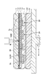
- step S1 the first substrate 11 and the chips 2A and 2B are bonded to obtain a laminated substrate.
- a first absorption layer 12 that absorbs a laser beam LB2, which will be described later
- a second absorption layer 13 that has a higher absorption coefficient with respect to the laser beam LB2 than the first absorption layer 12.
- the bonding layer 14 are formed in this order.
- the first substrate 11 is a silicon wafer.
- the first substrate 11 may be a compound semiconductor wafer.
- Compound semiconductor wafers are not particularly limited, but are, for example, GaAs wafers, SiC wafers, GaN wafers, InP wafers, or AlN wafers.
- the first absorption layer 12 is arranged between the first substrate 11 and the chips 2A, 2B. Although the details will be described later, as shown in FIG. 5 , the laser beam LB2 passes through the first substrate 11 and irradiates the first absorption layer 12 .
- the laser beam LB ⁇ b>2 is absorbed by the first absorption layer 12 to form a modified layer M in the first absorption layer 12 .
- the first absorption layer 12 is, for example, a silicon oxide layer, and is formed by a thermal oxidation method, a CVD (Chemical Vapor Deposition) method, or the like.
- the first absorption layer 12 may be a silicon nitride layer, a silicon carbonitride layer, or the like as long as it can absorb the laser beam LB2 to the extent that the modified layer M can be formed.
- the silicon nitride layer is formed by thermal nitridation, CVD, or the like.
- the silicon carbonitride layer is formed by a CVD method or the like.
- the second absorption layer 13 absorbs the laser beam LB2 that was not completely absorbed by the first absorption layer 12. Since the chips 2A and 2B are hardly irradiated with the laser beam LB2, damage to the chips 2A and 2B, especially the device layers 22A and 22B can be suppressed.
- the second absorption layer 13 has a higher absorption coefficient with respect to the laser beam LB2 than the first absorption layer 12 . Therefore, compared to the case where the first absorption layer 12 alone absorbs the laser beam LB2 to the same extent, the thickness of the entire layer can be reduced.
- the second absorption layer 13 transmits the detection light LB1.
- the detection light LB1 is used to detect the alignment mark 15.
- the alignment marks 15 are used for alignment during bonding between the first substrate 11 and the chips 2A and 2B, or for measuring misalignment after bonding. Alignment marks 15 may be used for both alignment and misalignment measurement.
- the measurement result of the misalignment after bonding is used, for example, for alignment when bonding the first substrate 11 and the chip on and after the next time.
- the measurement result of the positional deviation after bonding may be used for quality control such as discrimination of defective products.
- the alignment mark 15 is formed, for example, between the first substrate 11 and the first absorption layer 12 . As will be described later, after the first substrate 11 and the chips 2A and 2B are separated from the modified layer M formed in the first absorption layer 12, the alignment mark 15 remains attached to the first substrate 11. (see FIG. 6). Therefore, when the first substrate 11 is reused, the alignment mark 15 can be reused without having to re-form the alignment mark 15 .
- the alignment mark 15 is detected using the detection light LB1.
- the detection light LB1 is applied to the alignment mark 15 in a direction opposite to that of the laser light LB2, and is applied to the alignment mark 15 from the side opposite to the first substrate 11, for example.
- the detection light LB ⁇ b>1 passes through the bonding layer 14 , the second absorption layer 13 , and the first absorption layer 12 and irradiates the alignment mark 15 .
- the detection light LB1 is, for example, infrared.
- the alignment mark 15 is captured by, for example, an infrared camera.
- the wavelength of the detection light LB1 is, for example, 1000 nm to 2000 nm, preferably 1000 nm to 1200 nm, different from the wavelength of the laser light LB2.
- the alignment mark 15 absorbs the detection light LB1, for example.
- the light source of the detection light LB1 and the infrared camera are arranged with the alignment mark 15 interposed therebetween.
- the alignment mark 15 may reflect the detection light LB1.
- the light source of the detection light LB1 and the infrared camera are arranged on one side (same side) of the alignment mark 15 .
- the alignment mark 15 transmits the laser beam LB2, as shown in FIG.
- the laser beam LB2 is transmitted through the first substrate 11 and the alignment marks 15 to form the modified layer M in the first absorption layer 12 .
- a plurality of modified layers M are formed on the dividing surface D. As shown in FIG.
- the dividing plane D may be set inside the first absorption layer 12 or may be set at the interface between the first absorption layer 12 and the first substrate 11 .
- the wavelength of the laser beam LB2 is, for example, 8800 nm to 11000 nm.
- the alignment mark 15 has a transmittance of the laser beam LB2 of, for example, 45% or more and 100% or less, preferably 50% or more and 100% or less, and more preferably 60% or more and 100% or less.
- the alignment mark 15 may absorb the detection light LB1 and transmit the laser light LB2.
- the alignment mark 15 is composed of, for example, a Ge film, a SiGe film, a metal silicide film, or an AlN film.
- the alignment mark 15 may reflect the detection light LB1 and transmit the laser light LB2.
- the second absorption layer 13 transmits the detection light LB1 and absorbs the laser light LB2.
- the second absorption layer 13 is a so-called cold filter or the like.
- the material of the high refractive index layer is, for example, titanium oxide or ruthenium oxide.
- the material of the low refractive index layer is silicon oxide, for example.
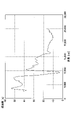
- FIG. 17A shows an example of the transmittance of a cold filter in which the total number of titanium oxide layers and silicon oxide layers is 40 and the total thickness is 3.5 ⁇ m.
- FIG. 17B shows an example of the transmittance of a cold filter having 20 titanium oxide layers and 20 silicon oxide layers and a total thickness of 1.56 ⁇ m.
- FIG. 17C shows an example of the transmittance of a cold filter having a total thickness of 0.82 ⁇ m with a total of 10 titanium oxide layers and silicon oxide layers.
- the total number of titanium oxide layers and silicon oxide layers is preferably set in the range of 10 to 20.
- 17A to 17C show the results obtained by simulating the transmittance of the cold filter alone (without the silicon substrate).
- FIGS. 18A and 18B show.
- FIG. 18B is a partially enlarged view of FIG. 18A.
- the transmittance was 40% or less when the wavelength was 8800 nm to 11000 nm.
- the transmittance was 5% or less.
- FIG. 19 shows TEM images of the silicon substrate and the cold filter used to measure the transmittance of FIGS. 18A and 18B.
- Si SiO 2
- TiO 2 are the materials of each layer, and the numbers in parentheses are the thickness of each layer.
- the bonding layer 14 is arranged between the second absorption layer 13 and the chips 2A, 2B as shown in FIG. 2, and contacts the chips 2A, 2B.
- the bonding layer 14 is, for example, an insulating layer such as a silicon oxide layer.
- the bonding layer 14 may be made of a material different from that of the first absorption layer 12, or may be made of the same material.
- the bonding surface of the bonding layer 14 facing the chips 2A and 2B may be surface-modified with plasma or the like before bonding, and may be made hydrophilic with pure water or the like.
- Surface modification breaks SiO 2 bonds on the joint surface, forms dangling bonds of Si, and makes it possible to hydrophilize the joint surface.
- oxygen gas which is a processing gas
- the bonding surface is irradiated with oxygen ions to modify the bonding surface.
- the processing gas is not limited to oxygen gas, and may be, for example, nitrogen gas.
- hydrophilization for example, pure water such as DIW (deionized water) is supplied to the joint surface rotated by the spin chuck.
- DIW deionized water
- An OH group is attached to a dangling bond of Si on the joint surface, and the joint surface is hydrophilized.
- the chip 2A has a second substrate 21A and a device layer 22A.
- the device layer 22A is formed on the surface of the second substrate 21A.
- the second substrate 21A is, for example, a silicon wafer, but may be a compound semiconductor wafer.
- the device layer 22A includes semiconductor elements, circuits, terminals, or the like.
- the device layer 22A may include at least one of transistors, element isolation, and wiring. After forming the device layer 22A, the second substrate 21A is singulated into a plurality of chips 2A.
- the chip 2B like the chip 2A, has a second substrate 21B and a device layer 22B.
- the second substrate 21B is, for example, a silicon wafer, but may be a compound semiconductor wafer.
- the device layer 22B has a function different from that of the device layer 22A, and has a thickness different from that of the chip 2A and chip 2B.
- the device layer 22B may include at least one of transistors, element isolation, and wiring. After forming the device layer 22B, the second substrate 21B is separated into a plurality of chips 2B.
- the bonding surfaces of the chips 2A and 2B facing the bonding layer 14 may be surface-modified with plasma or the like before bonding, and may be made hydrophilic with pure water or the like.
- step S1 the chips 2A and 2B are temporarily bonded to the first substrate 11 one by one.
- Chips 2A and 2B are bonded to first substrate 11 with device layers 22A and 22B facing first substrate 11 .
- the chips 2A and 2B and the first substrate 11 are bonded by van der Waals forces (intermolecular forces) and hydrogen bonds between OH groups without using a liquid adhesive. After that, heat treatment may be performed in order to increase the bonding strength.
- the chips 2A, 2B are temporarily bonded to the first substrate 11 and separated from the first substrate 11 later. Therefore, even if the chips 2A, 2B and the first substrate 11 are joined together, even if air bubbles get into the chips, there is no problem. Therefore, in step S1, the chips 2A and 2B can be bonded to the first substrate 11 while being held flat. Since the chips 2A and 2B are not deformed, the accuracy of the position control of the chips 2A and 2B can be improved, and the chips 2A and 2B can be accurately placed at the target positions.
- the chips 2A and 2B are temporarily bonded to the first substrate 11 and separated from the first substrate 11 later. Therefore, even if particles are caught when the chips 2A, 2B and the first substrate 11 are joined, no problem occurs. Therefore, the bonding surface of the bonding layer 14 and the bonding surfaces of the chips 2A and 2B may be dirty to the extent that bonding is not hindered. Requires less cleanliness.
- step S2 although not shown, the chips 2A and 2B are thinned to make the thicknesses of the chips 2A and 2B uniform.
- the second substrates 21A, 21B are thinned, and the device layers 22A, 22B are not thinned.
- Thinning includes grinding or laser processing.
- the bonding layer 3 is formed on the surfaces of the chips 2A and 2B.
- the bonding layer 3 is an insulating layer such as a silicon oxide layer, and is formed by the CVD method or the like.
- the chips 2A, 2B are spaced apart to form an uneven surface. Since the bonding layer 3 is formed on the uneven surface, the surface of the bonding layer 3 also has unevenness.
- step S4 as shown in FIG. 3, the surface of the bonding layer 3 is flattened.
- the planarization of the surface of the bonding layer 3 includes, for example, laser processing and CMP (Chemical Mechanical Polishing) in this order.
- the CMP time can be shortened by removing the protrusions by laser processing.
- step S4 may include only one of laser processing and CMP.
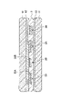
- step S5 the chips 2A and 2B and the third substrate 51 are bonded as shown in FIG.
- a bonding layer 52 is formed on the bonding surface of the third substrate 51 facing the chips 2A and 2B.
- the third substrate 51 is, for example, a silicon wafer, but may be a compound semiconductor wafer.
- the bonding layer 52 is an insulating layer such as a silicon oxide layer, and is formed by a CVD method or the like.
- the chips 2A and 2B and the third substrate 51 are bonded by van der Waals forces (intermolecular forces) and hydrogen bonds between OH groups without using a liquid adhesive.
- the third substrate 51 is deformed into a downwardly convex curved surface in order to prevent air bubbles from entering, and is gradually bonded from the center toward the periphery, and finally returns to a flat surface.
- the deformation of the third substrate 51 can be achieved by fixing the periphery of the third substrate 51 and pressing the center of the third substrate 51 .
- the deformation is easy. The reason why the deformation is easy is that the substrates are bonded to each other.
- the arrangement of the third substrate 51 and the first substrate 11 may be reversed, and the third substrate 51 may be arranged below the first substrate 11 .
- the third substrate 51 is deformed into an upwardly convex curved surface in order to prevent entrapment of air bubbles.
- the third substrate 51 is first bent and deformed, but the first substrate 11 is first bent and deformed. good too.
- step S6 the first substrate 11 is irradiated with a laser beam LB2 from the side opposite to the second substrates 21A and 21B, and the laser beam LB2 transmitted through the first substrate 11 is
- the first absorption layer 12 is irradiated to form a modified layer M in the first absorption layer 12 .
- a plurality of modified layers M are formed on the dividing surface D.
- the modified layer M is formed in a dot shape, and is formed, for example, at a condensing point or above the condensing point.
- the laser beam LB2 passes through the first substrate 11 and irradiates the first absorption layer 12 to form a modified layer M in the first absorption layer 12 .
- the first absorption layer 12 is arranged between the first substrate 11 and the chips 2A and 2B and absorbs the laser beam LB2.
- the second absorption layer 13 is arranged between the first absorption layer 12 and the chips 2A and 2B, and absorbs the laser beam LB2 that has not been completely absorbed by the first absorption layer 12 . Since the chips 2A and 2B are hardly irradiated with the laser beam LB2, damage to the chips 2A and 2B, especially the device layers 22A and 22B can be suppressed.
- the laser beam LB2 has a wavelength of 8800 nm to 11000 nm, for example, so that it can pass through the first substrate 11 and the alignment marks 15 and be absorbed by the first absorption layer 12 .
- a light source of the laser beam LB2 is, for example, a CO 2 laser.
- the wavelength of CO2 laser is about 9300 nm.
- the laser beam LB2 is pulse-oscillated.
- the formation position of the modified layer M is moved by a galvanometer scanner or an XY ⁇ stage.
- the galvanometer scanner moves laser beam LB2.
- the XY ⁇ stage moves the first substrate 11 in the horizontal direction (X-axis direction and Y-axis direction) and rotates it around the vertical axis.
- An XYZ ⁇ stage may be used instead of the XY ⁇ stage.
- a plurality of modified layers M are formed at intervals in the circumferential direction and radial direction of the first substrate 11 .
- cracks CR connecting the modified layers M are also formed.
- step S7 starting from the modified layer M, the first substrate 11 and the second substrates 21A and 21B are separated, and the chips 2A and 2B and the first substrate 11 are separated, as shown in FIG.
- the upper chuck 131 holds the first substrate 11 and the lower chuck 132 holds the third substrate 51 .
- the first substrate 11 and the third substrate 51 may be arranged upside down, and the upper chuck 131 may hold the third substrate 51 and the lower chuck 132 may hold the first substrate 11 .
- the crack CR spreads planarly starting from the modified layer M, and the chips 2A and 2B and the first substrate 11 are separated at the dividing surface D.
- the upper chuck 131 may be rotated around the vertical axis as the upper chuck 131 is lifted.
- the first substrate 11 and the second substrates 21A and 21B can be threaded at the dividing plane D.
- the downward movement of the lower chuck 132 may be performed.
- rotation of the lower chuck 132 about the vertical axis may be performed.
- a part of the first absorption layer 12, the second absorption layer 13, and the bonding layer 14 remaining on the chips 2A and 2B may be removed by CMP or the like. good. This exposes the device layers 22A, 22B of the chips 2A, 2B again.
- the device layers 22A and 22B are semiconductor memories, for example.
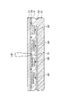
- step S8 the chips 2A and 2B are bonded to the device layer 62 formed on the fourth substrate 61 while being bonded to the third substrate 51, as shown in FIG.
- the fourth substrate 61 is, for example, a silicon wafer, but may be a compound semiconductor wafer.
- the device layer 62 includes semiconductor elements, circuits, terminals, or the like, and is electrically connected to the device layers 22A, 22B of the chips 2A, 2B.
- the device layer 62 is, for example, a semiconductor memory peripheral circuit (also called “peripheral”) or a semiconductor memory input/output circuit (also called “IO”).
- the chips 2A and 2B and the fourth substrate 61 are bonded by van der Waals forces (intermolecular forces) and hydrogen bonds between OH groups without using a liquid adhesive.
- the fourth substrate 61 is deformed into a downward convex curved surface in order to prevent air bubbles from entering, and is gradually bonded from the center toward the periphery, and finally returns to a flat surface.
- the deformation of the fourth substrate 61 can be realized by fixing the periphery of the fourth substrate 61 and pressing down the center of the fourth substrate 61 .
- the deformation is easy. The reason why the deformation is easy is that the substrates are bonded to each other.
- the arrangement of the fourth substrate 61 and the third substrate 51 may be reversed, and the fourth substrate 61 may be arranged below the third substrate 51 .
- the fourth substrate 61 is deformed into an upwardly convex curved surface in order to prevent air bubbles from entering.
- the fourth substrate 61 is first bent and deformed, but the third substrate 51 is first bent and deformed. good too.
- a substrate with a chip is obtained by the above step S8.
- the substrate with chips includes a fourth substrate 61 and a plurality of chips 2A and 2B.
- the chip-equipped substrate further includes a third substrate 51 . Note that the third substrate 51 may be separated from the chips 2A and 2B, and the chip-attached substrate may include the fourth substrate 61 and the chips 2A and 2B.
- the chips 2A and 2B in order to obtain a substrate with chips, instead of bonding the plurality of chips 2A and 2B one by one to one side of the fourth substrate 61, first the first substrate 11 is formed. temporarily bonded to one side of the Since entrapment of air bubbles at this stage does not pose a problem, the chips 2A and 2B can be bonded to the first substrate 11 while being held flat. Since the chips 2A and 2B do not have to be forcibly deformed, the accuracy of the position control of the chips 2A and 2B can be improved, and the chips 2A and 2B can be accurately placed at the target positions.
- the plurality of chips 2A and 2B bonded to the first substrate 11 are bonded to the third substrate 51.
- the chips 2A and 2B and the first substrate 11 are separated.
- the plurality of chips 2A and 2B are bonded to the device layer 62 formed on the fourth substrate 61 while being bonded to the third substrate 51 .
- the fourth substrate 61 is deformed into a curved surface in order to prevent air bubbles from entering, and is gradually bonded from the center toward the periphery, and finally returns to a flat surface.
- Deforming the fourth substrate 61 is easier than deforming the chips 2A and 2B one by one. This is because substrates are bonded together. Therefore, compared to the case of permanently bonding the chips 2A and 2B to the fourth substrate 61 without going through the step of temporarily bonding the chips 2A and 2B to the first substrate 11, there is no entrapment of air bubbles. , a chip-attached substrate with good positional accuracy can be obtained.
- alignment marks 15 are attached to the first substrate 11 after the chips 2A and 2B and the first substrate 11 are separated. Therefore, when the first substrate 11 is reused, the alignment mark 15 can be reused without having to re-form the alignment mark 15 .
- FIG. 8 a second embodiment of the substrate processing method shown in FIG. 1 will be described with reference to FIGS. 8 to 12.
- FIG. 8 alignment marks 15 are arranged between the second absorption layer 13 and the chips 2A, 2B.
- differences between the second embodiment and the first embodiment will be mainly described.
- step S1 the first substrate 11 and the chips 2A and 2B are bonded to obtain a laminated substrate.
- a first absorption layer 12 that absorbs a laser beam LB2, which will be described later, and an absorption coefficient for the laser beam LB2 that is higher than that of the first absorption layer 12 are formed.
- the tall second absorption layer 13 and the bonding layer 14 may be formed in this order.
- the alignment mark 15 is detected using the detection light LB1 as in the first embodiment.
- the detection light LB1 is applied to the alignment mark 15 in a direction opposite to that of the laser light LB2, and is applied to the alignment mark 15 from the side opposite to the first substrate 11, for example.
- the detection light LB1 passes, for example, between the adjacent chips 2A and 2B and irradiates the alignment mark 15. As shown in FIG.
- the alignment mark 15 reflects the detection light LB1, for example.
- the reflectance can be adjusted with a refractive index difference.
- the alignment mark 15 reflects the detection light LB ⁇ b>1
- the light source of the detection light LB ⁇ b>1 and the infrared camera are arranged on one side (the same side) of the alignment mark 15 .
- the second absorption layer 13 absorbs the detection light LB1
- the second absorption layer 13 of the first embodiment transmits the detection light LB1 as described above. This is because the detection light LB1 of the first embodiment is applied to the alignment mark 15 through the second absorption layer 13 as shown in FIG.
- the alignment marks 15 are arranged between the second absorption layer 13 and the chips 2A and 2B, unlike the first embodiment, and are formed, for example, on the bonding surface of the bonding layer 14 facing the chips 2A and 2B. As will be described later, after the first substrate 11 and the chips 2A and 2B are separated from the modified layer M formed in the first absorption layer 12, the alignment marks 15 remain attached to the chips 2A and 2B. (see FIG. 12). Therefore, the alignment marks 15 can be used in post-processing of the chips 2A and 2B.
- the alignment mark 15 is not formed between the first substrate 11 and the first absorption layer 12. Therefore, the alignment mark 15 does not have to transmit the laser beam LB2, and even if it absorbs the laser beam LB2, the alignment mark 15 does not have to pass therethrough. good. As shown in FIG. 11 , the laser beam LB2 passes through the first substrate 11 and irradiates the first absorption layer 12 to form a modified layer M in the first absorption layer 12 .
- the second absorption layer 13 absorbs the laser beam LB2 that was not completely absorbed by the first absorption layer 12, as in the first embodiment. Since the chips 2A and 2B are hardly irradiated with the laser beam LB2, damage to the chips 2A and 2B, especially the device layers 22A and 22B can be suppressed.
- the second absorption layer 13 has a higher absorption coefficient with respect to the laser beam LB2 than the first absorption layer 12 . Therefore, compared to the case where the first absorption layer 12 alone absorbs the laser beam LB2 to the same extent, the thickness of the entire layer can be reduced.
- the second absorption layer 13 absorbs the detection light LB1 unlike the first embodiment. In the image captured by the infrared camera, there is a large difference in brightness between the alignment mark 15 and its surroundings, and the detection accuracy of the alignment mark 15 is high.
- the second absorbent layer 13 contains, for example, a black absorbent.
- a black absorber contains black titanium or black carbon, for example.
- step S2 although not shown, the chips 2A and 2B are thinned to make the thicknesses of the chips 2A and 2B uniform.
- step S3 although not shown, the bonding layer 3 is formed on the surfaces of the chips 2A and 2B.
- step S4 as shown in FIG. 9, the surface of the bonding layer 3 is flattened.
- step S5 as shown in FIG. 10, the chips 2A and 2B and the third substrate 51 are bonded.
- step S6 the first substrate 11 is irradiated with a laser beam LB2 from the side opposite to the second substrates 21A and 21B, and the laser beam LB2 transmitted through the first substrate 11 is
- the first absorption layer 12 is irradiated to form a modified layer M in the first absorption layer 12 .
- a plurality of modified layers are formed on the dividing surface D.
- the first absorption layer 12 is arranged between the first substrate 11 and the chips 2A and 2B and absorbs the laser beam LB2.
- the second absorption layer 13 is arranged between the first absorption layer 12 and the chips 2A and 2B, and absorbs the laser beam LB2 that has not been completely absorbed by the first absorption layer 12 . Since the chips 2A and 2B are hardly irradiated with the laser beam LB2, damage to the chips 2A and 2B, especially the device layers 22A and 22B can be suppressed.
- step S7 starting from the modified layer M, the first substrate 11 and the second substrates 21A and 21B are separated, and the chips 2A and 2B and the first substrate 11 are separated, as shown in FIG.
- the crack CR spreads planarly, and the chips 2A and 2B and the first substrate 11 are separated at the dividing surface D.
- a part of the first absorption layer 12, the second absorption layer 13, and the bonding layer 14 remaining on the chips 2A and 2B may be removed by CMP or the like. good. This exposes the device layers 22A, 22B of the chips 2A, 2B again.
- the device layers 22A and 22B are semiconductor memories, for example.
- step S8 as shown in FIG. 7, the chips 2A and 2B are bonded to the third substrate 51, and the device layer 62 formed on the fourth substrate 61 and the device layer 62 are bonded together as shown in FIG. Join.
- the device layer 62 is electrically connected to the device layers 22A, 22B of the chips 2A, 2B.
- the device layer 62 is, for example, a semiconductor memory peripheral circuit or an input/output circuit.
- a substrate with a chip is obtained by the step S8.
- FIG. 13 After the first absorption layer 12 is irradiated with the laser beam LB2, the alignment mark 15 is irradiated with the detection beam LB1. Further, in the third embodiment, the alignment mark 15 is irradiated with the detection light LB1 in the same direction as the laser light LB2.
- the third embodiment differences between the third embodiment and the second embodiment will be mainly described.
- the first substrate 11 is irradiated with the laser beam LB2 from the side opposite to the second substrates 21A and 21B.
- a modified layer M is formed in the first absorption layer 12 by irradiating the first absorption layer 12 with the laser beam LB2 that has passed through the first substrate 11 .
- a plurality of modified layers are formed on the dividing surface D. As shown in FIG.
- the first substrate 11 and the second substrates 21A and 21B are separated from the modified layer M as shown in FIG. Chips 2A and 2B and first substrate 11 are separated.
- alignment marks 15 remain on the chips 2A and 2B.
- a part of the first absorption layer 12 and the second absorption layer 13 also remain on the chips 2A, 2B.
- part of the first absorption layer 12 and the second absorption layer 13 are removed by CMP or the like.
- the bonding layer 14 may be removed or not removed as shown in FIG.
- Alignment marks 15 remain on chips 2A and 2B without being removed. Therefore, as will be described later, the alignment marks 15 can be used in the post-processing of the chips 2A and 2B.
- an insulating layer 81 is formed on the chips 2A and 2B.
- the insulating layer 81 is, for example, a silicon oxide layer.
- Alignment marks 15 are used for adjusting the positions of vias formed in insulating layer 81 . Alignment mark 15 is detected using detection light LB1.
- the detection light LB1 is irradiated onto the alignment mark 15 in the same direction as the laser light LB2, for example.
- the detection light LB ⁇ b>1 passes through the insulating layer 81 and the bonding layer 14 and irradiates the alignment mark 15 .
- the alignment mark 15 may absorb or reflect the detection light LB1.
- the detection light LB1 is, for example, infrared light, and the alignment mark 15 is imaged by, for example, an infrared camera.
- the detection light LB1 is irradiated onto the alignment mark 15 in the same direction as the laser light LB2, as described above. It is not necessary to turn the chips 2A and 2B upside down between irradiation with the laser light LB2 and irradiation with the detection light LB1. Therefore, a mechanism for vertically inverting the chips 2A and 2B is not required, and the structure of the substrate processing apparatus can be simplified.
- the second absorption layer 13 since the second absorption layer 13 is removed before the irradiation of the detection light LB1, the second absorption layer 13 does not have to transmit the detection light LB1. Therefore, the second absorption layer 13 may be made of a material that absorbs the laser light LB2 and the detection light LB1. The structure of the second absorption layer 13 can be simplified.
- the second absorbent layer 13 contains, for example, a black absorbent.
- the fourth embodiment unlike the third embodiment, the second absorption layer 13 is left without removing the second absorption layer 13 by CMP or the like after the chips 2A and 2B and the first substrate 11 are separated. Differences between the fourth embodiment and the third embodiment will be mainly described below.
- the insulating layer 81 is formed on the second absorption layer 13 when forming the insulating layer 81 on the chips 2A and 2B.
- the insulating layer 81 is, for example, a silicon oxide layer.
- Alignment marks 15 are used for adjusting the positions of vias formed in insulating layer 81 . Alignment mark 15 is detected using detection light LB1.
- the detection light LB1 is irradiated onto the alignment mark 15 in the same direction as the laser light LB2, for example.
- the detection light LB ⁇ b>1 passes through the insulating layer 81 , the second absorption layer 13 and the bonding layer 14 and irradiates the alignment mark 15 .
- the alignment mark 15 may absorb or reflect the detection light LB1.
- the detection light LB1 is, for example, infrared light, and the alignment mark 15 is imaged by, for example, an infrared camera.
- the detection light LB1 is irradiated onto the alignment mark 15 in the same direction as the laser light LB2, as described above. It is not necessary to turn the chips 2A and 2B upside down between irradiation with the laser light LB2 and irradiation with the detection light LB1. Therefore, a mechanism for vertically inverting the chips 2A and 2B is not required, and the structure of the substrate processing apparatus can be simplified.
- the detection light LB1 passes through the second absorption layer 13.
- the second absorption layer 13 absorbs the laser beam LB2 and transmits the detection beam LB1.
- the second absorption layer 13 is a so-called cold filter or the like.
- the chips 2A and 2B including the device layers 22A and 22B and the second substrates 21A and 21B are spaced apart.
- the technology of the present disclosure is not limited to C2W (Chip to Wafer), and may be applied to W2W (Wafer to Wafer).
- the second substrate on which the device layer is formed may be bonded to the first substrate having the same size as the second substrate.
- the first substrate and the second substrate may have bonding surfaces of the same size, for example.
- the device layer formed on the second substrate and the first substrate are separated by separating the first substrate and the second substrate from the modified layer M as a starting point.
Landscapes
- Engineering & Computer Science (AREA)
- Physics & Mathematics (AREA)
- Optics & Photonics (AREA)
- Plasma & Fusion (AREA)
- Mechanical Engineering (AREA)
- Laser Beam Processing (AREA)
- Manufacturing & Machinery (AREA)
Priority Applications (4)
| Application Number | Priority Date | Filing Date | Title |
|---|---|---|---|
| CN202280037723.1A CN117397001A (zh) | 2021-06-03 | 2022-05-25 | 基板处理方法 |
| JP2023525756A JP7636087B2 (ja) | 2021-06-03 | 2022-05-25 | 基板処理方法 |
| KR1020237044085A KR20240016994A (ko) | 2021-06-03 | 2022-05-25 | 기판 처리 방법 |
| US18/562,502 US20240250064A1 (en) | 2021-06-03 | 2022-05-25 | Substrate processing method |
Applications Claiming Priority (2)
| Application Number | Priority Date | Filing Date | Title |
|---|---|---|---|
| JP2021-093400 | 2021-06-03 | ||
| JP2021093400 | 2021-06-03 |
Publications (1)
| Publication Number | Publication Date |
|---|---|
| WO2022255189A1 true WO2022255189A1 (ja) | 2022-12-08 |
Family
ID=84323136
Family Applications (1)
| Application Number | Title | Priority Date | Filing Date |
|---|---|---|---|
| PCT/JP2022/021409 Ceased WO2022255189A1 (ja) | 2021-06-03 | 2022-05-25 | 基板処理方法 |
Country Status (5)
| Country | Link |
|---|---|
| US (1) | US20240250064A1 (https=) |
| JP (1) | JP7636087B2 (https=) |
| KR (1) | KR20240016994A (https=) |
| CN (1) | CN117397001A (https=) |
| WO (1) | WO2022255189A1 (https=) |
Citations (3)
| Publication number | Priority date | Publication date | Assignee | Title |
|---|---|---|---|---|
| JPH10125929A (ja) * | 1996-08-27 | 1998-05-15 | Seiko Epson Corp | 剥離方法 |
| WO2020111146A1 (ja) * | 2018-11-29 | 2020-06-04 | 日立化成株式会社 | 半導体装置の製造方法及び仮固定材用積層フィルム |
| WO2021084902A1 (ja) * | 2019-10-29 | 2021-05-06 | 東京エレクトロン株式会社 | チップ付き基板の製造方法、及び基板処理装置 |
Family Cites Families (9)
| Publication number | Priority date | Publication date | Assignee | Title |
|---|---|---|---|---|
| US7534498B2 (en) * | 2002-06-03 | 2009-05-19 | 3M Innovative Properties Company | Laminate body, method, and apparatus for manufacturing ultrathin substrate using the laminate body |
| US7195813B2 (en) * | 2004-05-21 | 2007-03-27 | Eastman Kodak Company | Mixed absorber layer for displays |
| JP6149277B2 (ja) * | 2011-03-30 | 2017-06-21 | ボンドテック株式会社 | 電子部品実装方法、電子部品実装システムおよび基板 |
| EP2810300A4 (en) | 2012-01-30 | 2016-05-11 | 3M Innovative Properties Co | DEVICE, HYBRID LAMINATED BODY, METHOD AND MATERIALS FOR TEMPORARY SUBSTRATE CARRIER |
| JP6034625B2 (ja) | 2012-09-03 | 2016-11-30 | 東京応化工業株式会社 | 剥離方法 |
| KR20250102102A (ko) * | 2016-12-23 | 2025-07-04 | 더 보드 오브 리젠츠 오브 더 유니버시티 오브 텍사스 시스템 | 무아레 기반 측정법과 진공 기반 취출 및 거치법을 사용하는 콤팩트 디바이스들 상의 구성소자들의 혼종 집적 |
| US10217637B1 (en) * | 2017-09-20 | 2019-02-26 | International Business Machines Corporation | Chip handling and electronic component integration |
| CN110824599B (zh) * | 2018-08-14 | 2021-09-03 | 白金科技股份有限公司 | 一种红外带通滤波器 |
| JP7281545B2 (ja) * | 2019-07-02 | 2023-05-25 | 旭化成株式会社 | バイオアッセイ用微細ウェルフィルム、バイオアッセイ用微細ウェルフィルム形成用感光性樹脂組成物、及び、バイオアッセイ用微細ウェルフィルムの製造方法 |
-
2022
- 2022-05-25 US US18/562,502 patent/US20240250064A1/en active Pending
- 2022-05-25 CN CN202280037723.1A patent/CN117397001A/zh active Pending
- 2022-05-25 WO PCT/JP2022/021409 patent/WO2022255189A1/ja not_active Ceased
- 2022-05-25 JP JP2023525756A patent/JP7636087B2/ja active Active
- 2022-05-25 KR KR1020237044085A patent/KR20240016994A/ko active Pending
Patent Citations (3)
| Publication number | Priority date | Publication date | Assignee | Title |
|---|---|---|---|---|
| JPH10125929A (ja) * | 1996-08-27 | 1998-05-15 | Seiko Epson Corp | 剥離方法 |
| WO2020111146A1 (ja) * | 2018-11-29 | 2020-06-04 | 日立化成株式会社 | 半導体装置の製造方法及び仮固定材用積層フィルム |
| WO2021084902A1 (ja) * | 2019-10-29 | 2021-05-06 | 東京エレクトロン株式会社 | チップ付き基板の製造方法、及び基板処理装置 |
Also Published As
| Publication number | Publication date |
|---|---|
| JPWO2022255189A1 (https=) | 2022-12-08 |
| US20240250064A1 (en) | 2024-07-25 |
| KR20240016994A (ko) | 2024-02-06 |
| JP7636087B2 (ja) | 2025-02-26 |
| CN117397001A (zh) | 2024-01-12 |
Similar Documents
| Publication | Publication Date | Title |
|---|---|---|
| JP7330284B2 (ja) | チップ付き基板の製造方法、及び基板処理装置 | |
| US8642444B2 (en) | Method of manufacturing bonded substrate, bonded substrate, method of manufacturing solid-state imaging apparatus, solid-state imaging apparatus, and camera | |
| TWI404196B (zh) | 固體攝像元件模組之製造方法 | |
| JP6395600B2 (ja) | 撮像装置の製造方法および半導体装置の製造方法 | |
| US7851880B2 (en) | Solid-state imaging device | |
| US8980671B2 (en) | Semiconductor device and manufacturing method of semiconductor device | |
| TW200804172A (en) | Semiconductor apparatus and method for manufacturing the same | |
| JP2005340423A (ja) | 半導体装置の製造方法 | |
| JP2017103478A (ja) | 撮像装置、半導体装置および撮像ユニット | |
| KR20140138898A (ko) | 초박막 웨이퍼의 임시 본딩을 위한 방법 및 장치 | |
| WO2016127645A1 (zh) | 封装方法及封装结构 | |
| WO2013179764A1 (ja) | 撮像装置の製造方法および半導体装置の製造方法 | |
| WO2013179767A1 (ja) | 撮像装置の製造方法および半導体装置の製造方法 | |
| US7105381B2 (en) | Wafer alignment method | |
| JPWO2020022015A1 (ja) | 接合方法および接合装置 | |
| CN115579374B (zh) | 背照式图像传感器的制备方法及背照式图像传感器 | |
| JP7636087B2 (ja) | 基板処理方法 | |
| CN118737958A (zh) | 半导体器件及其制作方法 | |
| KR20230135615A (ko) | 칩 포함 기판 제조 방법 및 기판 처리 장치 | |
| CN114975501A (zh) | 晶圆键合方法以及背照式图像传感器的形成方法 | |
| TWI917180B (zh) | 附有晶片之基板的製造方法 | |
| JP4926630B2 (ja) | 固体撮像装置の製造方法および製造装置、並びに貼付装置 | |
| CN204497233U (zh) | 封装结构 | |
| CN121398602A (zh) | 用于晶圆键合的半导体结构及其改善晶圆键合对准的方法 | |
| CN117096165A (zh) | 图像传感器封装结构及相关方法 |
Legal Events
| Date | Code | Title | Description |
|---|---|---|---|
| 121 | Ep: the epo has been informed by wipo that ep was designated in this application |
Ref document number: 22815939 Country of ref document: EP Kind code of ref document: A1 |
|
| WWE | Wipo information: entry into national phase |
Ref document number: 18562502 Country of ref document: US Ref document number: 2023525756 Country of ref document: JP |
|
| WWE | Wipo information: entry into national phase |
Ref document number: 202280037723.1 Country of ref document: CN |
|
| ENP | Entry into the national phase |
Ref document number: 20237044085 Country of ref document: KR Kind code of ref document: A |
|
| NENP | Non-entry into the national phase |
Ref country code: DE |
|
| 122 | Ep: pct application non-entry in european phase |
Ref document number: 22815939 Country of ref document: EP Kind code of ref document: A1 |