WO2022239102A1 - 半導体素子を用いたメモリ装置 - Google Patents
半導体素子を用いたメモリ装置 Download PDFInfo
- Publication number
- WO2022239102A1 WO2022239102A1 PCT/JP2021/017858 JP2021017858W WO2022239102A1 WO 2022239102 A1 WO2022239102 A1 WO 2022239102A1 JP 2021017858 W JP2021017858 W JP 2021017858W WO 2022239102 A1 WO2022239102 A1 WO 2022239102A1
- Authority
- WO
- WIPO (PCT)
- Prior art keywords
- layer
- conductor layer
- gate
- impurity
- semiconductor
- Prior art date
- Legal status (The legal status is an assumption and is not a legal conclusion. Google has not performed a legal analysis and makes no representation as to the accuracy of the status listed.)
- Ceased
Links
Images







Classifications
-
- H—ELECTRICITY
- H10—SEMICONDUCTOR DEVICES; ELECTRIC SOLID-STATE DEVICES NOT OTHERWISE PROVIDED FOR
- H10B—ELECTRONIC MEMORY DEVICES
- H10B12/00—Dynamic random access memory [DRAM] devices
- H10B12/20—DRAM devices comprising floating-body transistors, e.g. floating-body cells
-
- G—PHYSICS
- G11—INFORMATION STORAGE
- G11C—STATIC STORES
- G11C11/00—Digital stores characterised by the use of particular electric or magnetic storage elements; Storage elements therefor
- G11C11/21—Digital stores characterised by the use of particular electric or magnetic storage elements; Storage elements therefor using electric elements
- G11C11/34—Digital stores characterised by the use of particular electric or magnetic storage elements; Storage elements therefor using electric elements using semiconductor devices
- G11C11/40—Digital stores characterised by the use of particular electric or magnetic storage elements; Storage elements therefor using electric elements using semiconductor devices using transistors
- G11C11/401—Digital stores characterised by the use of particular electric or magnetic storage elements; Storage elements therefor using electric elements using semiconductor devices using transistors forming cells needing refreshing or charge regeneration, i.e. dynamic cells
- G11C11/403—Digital stores characterised by the use of particular electric or magnetic storage elements; Storage elements therefor using electric elements using semiconductor devices using transistors forming cells needing refreshing or charge regeneration, i.e. dynamic cells with charge regeneration common to a multiplicity of memory cells, i.e. external refresh
- G11C11/404—Digital stores characterised by the use of particular electric or magnetic storage elements; Storage elements therefor using electric elements using semiconductor devices using transistors forming cells needing refreshing or charge regeneration, i.e. dynamic cells with charge regeneration common to a multiplicity of memory cells, i.e. external refresh with one charge-transfer gate, e.g. MOS transistor, per cell
-
- G—PHYSICS
- G11—INFORMATION STORAGE
- G11C—STATIC STORES
- G11C11/00—Digital stores characterised by the use of particular electric or magnetic storage elements; Storage elements therefor
- G11C11/21—Digital stores characterised by the use of particular electric or magnetic storage elements; Storage elements therefor using electric elements
- G11C11/34—Digital stores characterised by the use of particular electric or magnetic storage elements; Storage elements therefor using electric elements using semiconductor devices
- G11C11/40—Digital stores characterised by the use of particular electric or magnetic storage elements; Storage elements therefor using electric elements using semiconductor devices using transistors
- G11C11/401—Digital stores characterised by the use of particular electric or magnetic storage elements; Storage elements therefor using electric elements using semiconductor devices using transistors forming cells needing refreshing or charge regeneration, i.e. dynamic cells
- G11C11/4063—Auxiliary circuits, e.g. for addressing, decoding, driving, writing, sensing or timing
- G11C11/407—Auxiliary circuits, e.g. for addressing, decoding, driving, writing, sensing or timing for memory cells of the field-effect type
- G11C11/409—Read-write [R-W] circuits
- G11C11/4097—Bit-line organisation, e.g. bit-line layout, folded bit lines
-
- H—ELECTRICITY
- H10—SEMICONDUCTOR DEVICES; ELECTRIC SOLID-STATE DEVICES NOT OTHERWISE PROVIDED FOR
- H10B—ELECTRONIC MEMORY DEVICES
- H10B12/00—Dynamic random access memory [DRAM] devices
- H10B12/01—Manufacture or treatment
- H10B12/02—Manufacture or treatment for one transistor one-capacitor [1T-1C] memory cells
- H10B12/03—Making the capacitor or connections thereto
- H10B12/036—Making the capacitor or connections thereto the capacitor extending under the transistor
-
- H—ELECTRICITY
- H10—SEMICONDUCTOR DEVICES; ELECTRIC SOLID-STATE DEVICES NOT OTHERWISE PROVIDED FOR
- H10B—ELECTRONIC MEMORY DEVICES
- H10B12/00—Dynamic random access memory [DRAM] devices
- H10B12/01—Manufacture or treatment
- H10B12/02—Manufacture or treatment for one transistor one-capacitor [1T-1C] memory cells
- H10B12/05—Making the transistor
-
- H—ELECTRICITY
- H10—SEMICONDUCTOR DEVICES; ELECTRIC SOLID-STATE DEVICES NOT OTHERWISE PROVIDED FOR
- H10B—ELECTRONIC MEMORY DEVICES
- H10B12/00—Dynamic random access memory [DRAM] devices
- H10B12/30—DRAM devices comprising one-transistor - one-capacitor [1T-1C] memory cells
- H10B12/33—DRAM devices comprising one-transistor - one-capacitor [1T-1C] memory cells the capacitor extending under the transistor
-
- G—PHYSICS
- G11—INFORMATION STORAGE
- G11C—STATIC STORES
- G11C2211/00—Indexing scheme relating to digital stores characterized by the use of particular electric or magnetic storage elements; Storage elements therefor
- G11C2211/401—Indexing scheme relating to cells needing refreshing or charge regeneration, i.e. dynamic cells
- G11C2211/4016—Memory devices with silicon-on-insulator cells
Definitions
- the present invention is a memory device using semiconductor elements.
- the channel In a normal planar MOS transistor, the channel extends horizontally along the upper surface of the semiconductor substrate. In contrast, the SGT channel extends in a direction perpendicular to the upper surface of the semiconductor substrate (see Patent Document 1 and Non-Patent Document 1, for example). For this reason, the SGT enables a higher density semiconductor device compared to a planar MOS transistor.
- a DRAM Dynamic Random Access Memory
- a PCM Phase Change Memory
- Non-Patent Document 4 RRAM (Resistive Random Access Memory, see, for example, Non-Patent Document 4), MRAM (Magneto-resistive Random Access Memory, see, for example, Non-Patent Document 5) that changes the resistance by changing the direction of the magnetic spin by current ) can be highly integrated.
- DRAM memory cell see Non-Patent Document 6
- the present application relates to a dynamic flash memory that does not have resistance change elements or capacitors and can be configured only with MOS transistors.
- FIG. 7 shows the write operation of a DRAM memory cell composed of a single MOS transistor without the capacitor described above
- FIG. 8 shows problems in operation
- FIG. 7 shows the write operation of the DRAM memory cell.
- FIG. 7(a) shows a "1" write state.
- the memory cell is formed on the SOI substrate 101 and includes a source N + layer 103 (hereinafter, a semiconductor region containing a high concentration of donor impurities is referred to as an “N + layer”) to which a source line SL is connected.
- the drain N + layer 104 connected to the line BL, the gate conductive layer 105 connected to the word line WL, and the floating body 102 of the MOS transistor 110a.
- a memory cell of the DRAM is composed of these pieces.
- the SiO 2 layer 101 of the SOI substrate is in contact directly below the floating body 102 .
- the MOS transistor 110a When "1" is written to the memory cell composed of one MOS transistor 110a, the MOS transistor 110a is operated in the linear region. That is, the electron channel 107 extending from the source N + layer 103 has a pinch-off point 108 and does not reach the drain N + layer 104 connected to the bit line. In this way, both the bit line BL connected to the drain N + layer 104 and the word line WL connected to the gate conductive layer 105 are set at a high voltage, and the gate voltage is set to about 1/2 of the drain voltage. , the electric field strength is maximized at the pinch-off point 108 near the drain N + layer 104 .
- the holes 106 generated at the same time charge the floating body 102 . In this case, the generated holes contribute as increments of majority carriers because the floating body 102 is P-type Si.
- the floating body 102 is filled with the generated holes 106, and when the voltage of the floating body 102 becomes higher than that of the source N + layer 103 by Vb or more, the generated holes are discharged to the source N + layer 103.
- Vb is the built-in voltage of the PN junction between the source N + layer 103 and the floating body 102 of the P layer, which is about 0.7V.
- FIG. 7B shows the floating body 102 saturated with the generated holes 106 .
- FIG. 7(c) shows how the "1" write state is rewritten to the "0" write state.
- the voltage of the bit line BL is negatively biased, and the PN junction between the drain N + layer 104 and the floating body 102 of the P layer is forward biased.
- the holes 106 previously generated in the floating body 102 in the previous cycle flow to the drain N + layer 104 connected to the bit line BL.
- FIG. 7(b) filled with the generated holes 106 and 110b (FIG. 7(c)) from which the generated holes are ejected are stored.
- the state of the memory cell is obtained.
- the floating body 102 potential of the memory cell 110a filled with holes 106 will be higher than the floating body 102 without the generated holes. Therefore, the threshold voltage of memory cell 110a is lower than that of memory cell 110b. This state is shown in FIG. 7(d).
- the capacitance CFB of the floating body 102 is composed of the capacitance CWL between the gate connected to the word line and the floating body 102, and the source N + layer 103 connected to the source line.
- FIG. 9(a) shows the "1" write state
- FIG. 9(b) shows the "0" write state.
- Vb is written to the floating body 102 by writing "1”
- the floating body 102 is pulled down to a negative bias when the word line returns to 0 V at the end of writing.
- the negative bias becomes even deeper. Therefore, as shown in FIG. do not have.
- This small operating margin is a major problem of the present DRAM memory cell.
- Critoloveanu “A Compact Capacitor-Less High-Speed DRAM Using Field Effect-Controlled Charge Regeneration,” Electron Device Letters, Vol. 35, No.2, pp. 179-181 (2012) T. Ohsawa, K. Fujita, T. Higashi, Y. Iwata, T. Kajiyama, Y. Asao, and K. Sunouchi: “Memory design using a one-transistor gain cell on SOI,” IEEE JSSC, vol.37, No.11, pp1510-1522 (2002). T. Shino, N. Kusunoki, T. Higashi, T. Ohsawa, K. Fujita, K. Hatsuda, N. Ikumi, F.
- the memory device includes: a semiconductor body on a substrate, standing vertically or extending horizontally with respect to the substrate; a first gate insulating layer surrounding part or all of a side surface on one end side of the semiconductor base; a second gate insulating layer connected to the first gate insulating layer and surrounding part or all of the side surface of the semiconductor base on the other end side; a first gate conductor layer covering the first gate insulating layer; a second gate conductor layer covering the second gate insulating layer; a first impurity layer outside one end of the first gate conductor layer and a second impurity layer outside one end of the second gate conductor layer in the direction in which the semiconductor matrix extends; a second impurity layer which is between one or both of the first impurity layer and the second impurity layer and the semiconductor base body and has the same conductivity type as the first impurity layer and the second impurity layer; 3 impurity layer; a first wiring conductor layer connected to the first impurity
- the first impurity layer is formed by controlling the voltage applied to the first wiring conductor layer, the second wiring conductor layer, the third wiring conductor layer, and the fourth wiring conductor layer. and extracting either the electron group or the hole group, which are majority carriers remaining in the semiconductor matrix, from one or both of the second impurity layers to perform a memory erasing operation. (first invention).
- the impurity concentration of the third impurity layer is lower than the impurity concentrations of the first impurity layer and the second impurity layer and higher than the impurity concentration of the semiconductor matrix. (second invention).
- the wiring connected to the first impurity layer is a source line
- the wiring connected to the second impurity layer is a bit line
- the wiring connected to the first gate conductor layer is:
- a wiring connected to the second gate conductor layer, which is a first drive control line, is a word line, and is applied to the source line, the bit line, the first drive control line, and the word line.
- the memory erasing operation and the memory writing operation are performed according to the voltage applied to the memory (a third invention).
- the above second invention is characterized in that the third impurity layer is formed at a position connected to the second impurity layer connected to the bit line (fourth invention).
- the above second invention is characterized in that the third impurity layer is formed at a position connected to the first impurity layer connected to the source line (fifth invention).
- the third impurity layer is formed at both a position connected to the first impurity layer connected to the source line and a position connected to the bit line.
- the first gate capacitance between the first gate conductor layer and the semiconductor base is greater than the second gate capacitance between the second gate conductor layer and the semiconductor base. is large (seventh invention).
- the semiconductor matrix stands in a direction perpendicular to the substrate, and in plan view, the first impurity layer and the third impurity layer connected to the semiconductor matrix It is characterized in that it extends outside the semiconductor base body (eighth invention).
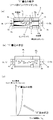
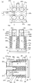
- FIG. 1 is a structural diagram of a memory device having SGTs according to the first embodiment
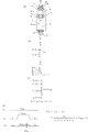
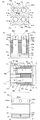
- FIG. FIG. 3 is a diagram for explaining an erase operation mechanism of a memory device having SGTs according to the first embodiment
- FIG. 4 is a diagram for explaining a write operation mechanism of a memory device having SGTs according to the first embodiment
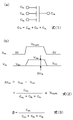
- FIG. 2 is a diagram for explaining a read operation mechanism of a memory device having SGTs according to the first embodiment
- FIG. 2 is a diagram for explaining a read operation mechanism of a memory device having SGTs according to the first embodiment
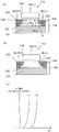
- FIG. 4 is a diagram for explaining a method of manufacturing a memory device having SGTs according to the first embodiment
- FIG. 1 is a structural diagram of a memory device having SGTs according to the first embodiment
- FIG. 3 is a diagram for explaining an erase operation mechanism of a memory device having SGTs according to the first embodiment
- FIG. 4 is a diagram for explaining a write operation mechanism of a memory device having SGTs according to the first
- FIG. 4 is a diagram for explaining a method of manufacturing a memory device having SGTs according to the first embodiment;
- FIG. 4 is a diagram for explaining a method of manufacturing a memory device having SGTs according to the first embodiment;
- FIG. 4 is a diagram for explaining a method of manufacturing a memory device having SGTs according to the first embodiment;
- FIG. 4 is a diagram for explaining a method of manufacturing a memory device having SGTs according to the first embodiment;
- FIG. 4 is a diagram for explaining a method of manufacturing a memory device having SGTs according to the first embodiment;
- FIG. 4 is a diagram for explaining a method of manufacturing a memory device having SGTs according to the first embodiment;
- FIG. 4 is a diagram for explaining a method of manufacturing a memory device having SGTs according to the first embodiment;
- FIG. 4 is a diagram for explaining a method of manufacturing a memory device having SGTs according to the first embodiment;
- FIG. 4 is a diagram for explaining a method of manufacturing
- FIG. 4 is a diagram for explaining a method of manufacturing a memory device having SGTs according to the first embodiment
- FIG. 10 is a diagram for explaining a method of manufacturing a memory device having SGTs according to the second embodiment
- FIG. 4 is a diagram for explaining operational problems of a conventional DRAM memory cell that does not have a capacitor
- FIG. 4 is a diagram for explaining operational problems of a conventional DRAM memory cell that does not have a capacitor
- FIG. 2 illustrates a read operation of a DRAM memory cell without a conventional capacitor
- dynamic flash memory a memory device using semiconductor elements
- FIG. 1 The structure, operation mechanism, and manufacturing method of the dynamic flash memory cell according to the first embodiment of the present invention will be described with reference to FIGS. 1 to 5.
- FIG. 1 The structure of a dynamic flash memory cell will be described with reference to FIG. Then, a data erasing mechanism will be described with reference to FIG. 2, a data writing mechanism will be described with reference to FIG. 3, and a data writing mechanism will be described with reference to FIG. A method of manufacturing a dynamic flash memory will be described with reference to FIG.
- FIG. 1 shows the structure of a dynamic flash memory cell according to a first embodiment of the invention.
- An N + layer 3a (which is an example of the "first impurity layer” in the claims) is provided on a substrate 1 (which is an example of the “substrate” in the claims).
- a silicon semiconductor pillar 2 having a conductivity type of P-type or i-type (intrinsic type) containing acceptor impurities (an example of a “semiconductor base” in the claims) (hereinafter referred to as silicon A semiconductor pillar is called a “Si pillar”.).
- N layer 8a (an example of the "third impurity layer” in the scope of claims) at the bottom of the Si pillar 2, N layer 8b (an example of the "third impurity layer” in the scope of claims) There is).
- N + layer 3b (which is an example of the "second impurity layer” in the scope of claims) on the N layer 8b.
- the donor impurity concentration of the N layers 8a, 8b is lower than that of the N + layers 3a, 3b.
- a portion of the Si pillar 2 between the N layers 8a and 8b becomes the channel region 7. As shown in FIG.
- a first gate insulating layer 4a (which is an example of the "first gate insulating layer” in the claims) and a second gate insulating layer 4b (the which is an example of the “second gate insulating layer” in the range).
- the first gate insulating layer 4a and the second gate insulating layer 4b are in contact with or close to the N layers 8a and 8b, respectively.
- Surrounding the first gate insulating layer 4a is a first gate conductor layer 5a (which is an example of the "first gate conductor layer” in the claims), and surrounding the second gate insulating layer 4b , and a second gate conductor layer 5b (which is an example of the "second gate conductor layer” in the claims).
- the first gate conductor layer 5 a and the second gate conductor layer 5 b are separated by an insulating layer 6 .
- N + layers 3a and 3b, N layer layers 8a and 8b, channel region 7, first gate insulating layer 4a, second gate insulating layer 4b, first gate conductor layer 5a, and second gate conductor layer are formed.
- a dynamic flash memory cell consisting of 5b is formed.
- the N + layer 3a serves as a source line SL (an example of a "source line” in the scope of claims), and the N + layer 3b serves as a bit line BL (an example of a "bit line” in the scope of claims).
- the first gate conductor layer 5a is connected to the plate line PL (an example of the "first drive control line” in the claims), and the second gate conductor layer 5b is connected to the word lines WL (claimed , which is an example of a "word line” of the
- the N layers 8a and 8b are composed of an N + layer 3a in which unwanted electrons are connected to the source line SL by voltages applied to the source line SL, the plate line PL, the word line WL, and the bit line BL of the dynamic flash memory, and the bit line SL.
- the structure is such that the gate capacitance of the first gate conductor layer 5a connected to the plate line PL is larger than the gate capacitance of the second gate conductor layer 5b connected to the word line WL. is desirable.
- a plurality of dynamic flash memory cells as described above are two-dimensionally arranged on the substrate 1 .
- the gate capacitance of the first gate conductor layer 5a connected to the plate line PL is made larger than the gate capacitance of the second gate conductor layer 5b connected to the word line WL.
- the gate length of the first gate conductor layer 5a is made longer than the gate length of the second gate conductor layer 5b.
- the gate length of the first gate conductor layer 5a is not made longer than the gate length of the second gate conductor layer 5b, and the thickness of the gate insulation film of the first gate insulation layer 4a is increased. , may be thinner than the thickness of the gate insulating film of the second gate insulating layer 4b.
- the dielectric constant of the first gate insulating layer 4a may be higher than that of the second gate insulating layer 4b.
- the gate capacitance of the first gate conductor layer 5a is determined by combining any one of the length of the gate conductor layers 5a and 5b, the film thickness of the gate insulating layers 4a and 4b, and the dielectric constant of the second gate conductor layer 5b. may be larger than the gate capacitance of
- the upper end position of the N layer 8a may be above or below the lower end position of the first gate conductor layer 5a.
- the lower end position of N layer 8b may be above or below the upper end position of second gate conductor layer 5b.
- first gate conductor layer 5a may be divided into two or more, each of which may be operated synchronously or asynchronously as a conductor electrode of a plate line.
- second gate conductor layer 5b may be divided into two or more, each of which may be operated synchronously or asynchronously as a conductor electrode of a word line. This also provides dynamic flash memory operation.
- the dynamic flash memory operation is also performed in a structure in which the conductivity polarities of the N + layers 3a and 3b, the N layers 8a and 8b, and the P-type Si pillar 2 are reversed.
- the N-type Si pillar majority carriers become electrons. Therefore, the electron group generated by impact ionization is stored in the channel region 7, and the "1" state is set.
- FIG. 2 illustrates the erase operation mechanism.
- Channel region 7 between N layers 8a and 8b is electrically isolated from the substrate and serves as a floating body.
- FIG. 2(a) shows a state in which the hole groups 11 generated by impact ionization in the previous cycle are stored in the channel region 7 before the erasing operation. and.
- the voltage of the bit line BL is set to the negative voltage VERA during the erase operation.
- VERA is, for example, -3V.
- V FB V ERA +Vb.
- the threshold voltage of the second gate conductor layer 5b connected to this word line WL is increased.
- the erased state of this channel region 7 is logical storage data "0".
- the voltage conditions applied to the bit line BL, the source line SL, the word line WL, and the plate line PL are only examples for performing the erase operation, and other operating conditions that enable the erase operation may be used.
- FIG. 3 shows the write operation of the dynamic flash memory cell according to the first embodiment of the invention.
- 0 V for example, is input to the N + layer 3a connected to the source line SL
- 3 V for example, is input to the N + layer 3b connected to the bit line BL
- the plate line PL 2 V for example, is input to the connected first gate conductor layer 5a
- 5 V for example, is input to the second gate conductor layer 5b connected to the word line WL.
- an annular inversion layer 12a is formed in the first channel region 7a inside the first gate conductor layer 5a connected to the plate line PL.
- the first N-channel MOS transistor with one gate conductor layer 5a is operated in the linear region.
- a pinch-off point 13 exists in the inversion layer 12a inside the first gate conductor layer 5a to which the plate line PL is connected.
- the second N-channel MOS transistor having the second gate conductor layer 5b connected to the word line WL is operated in the saturation region.
- the inversion layer 12b is formed on the entire surface of the second channel region 7b inside the second gate conductor layer 5b connected to the word line WL without any pinch-off point.
- the inversion layer 12b formed entirely inside the second gate conductor layer 5b connected to the word line WL serves as a substantial drain of the second N-channel MOS transistor having the second gate conductor layer 5b. work.
- the channel region 7 between the first N-channel MOS transistor having the first gate conductor layer 5a and the second N-channel MOS transistor having the second gate conductor layer 5b, which are connected in series has a second
- the electric field is maximum at the boundary region of 1 and the impact ionization phenomenon occurs in this region. Since this region is the region on the source side viewed from the second N-channel MOS transistor having the second gate conductor layer 5b connected to the word line WL, this phenomenon is called the source-side impact ionization phenomenon.
- the generated hole group 11 is majority carriers in the channel region 7 and charges the channel region 7 with a positive bias. Since the N + layer 3a connected to the source line SL is at 0 V, the channel region 7 is at the built-in voltage of the PN junction between the N + layer 3a connected to the source line SL, the N layer 8a and the channel region 7. It is charged to Vb (approximately 0.7V). When channel region 7 is positively biased, the threshold voltages of the first N-channel MOS transistor and the second N-channel MOS transistor are lowered due to the substrate bias effect. Thereby, as shown in FIG. 3(c), the threshold voltage of the N-channel MOS transistor in the second channel region 7b connected to the word line WL is lowered. The write state of this channel area 7 is assigned to logical storage data "1".
- a second boundary region between the N layer 8a and the first channel semiconductor layer 7a, or between the N layer 8b and the second channel semiconductor layer. 7b electron-hole pairs may be generated by impact ionization or GIDL current, and the channel region 7 may be charged with the generated hole groups 11.
- FIG. 1 The voltage conditions applied to the bit line BL, the source line SL, the word line WL, and the plate line PL are examples for performing the write operation, and other operating conditions that allow the write operation may be used.
- FIGS. 4A and 4B A read operation of the dynamic flash memory cell according to the first embodiment of the present invention will be described with reference to FIGS. 4A and 4B.
- the read operation of the dynamic flash memory cell will be described with reference to FIGS. 4A(a) to 4A(c).
- FIG. 4A(a) when channel region 7 is charged to built-in voltage Vb (approximately 0.7 V), the threshold voltage of the N-channel MOS transistor is lowered due to the substrate bias effect. This state is assigned to logical storage data "1".
- FIG. 4A(b) if the memory block selected before writing is in the erased state "0" in advance, the floating voltage V FB of the channel region 7 is V ERA +Vb.
- a write operation randomly stores a write state of "1". As a result, logical storage data of logical "0" and “1" are created for the word line WL.
- FIG. 4A(c) reading is performed by the sense amplifier using the level difference between the two threshold voltages
- the gate capacitance of the second gate conductor layer 5b connected to the word line WL is preferably designed to be smaller than the gate capacitance of the first gate conductor layer 5a connected to the plate line PL. As shown in FIG. 4B(a), the length in the vertical direction of the first gate conductor layer 5a connected to the plate line PL is equal to the length in the central axis direction of the second gate conductor layer 5b connected to the word line WL.
- FIG. 4B(b) shows an equivalent circuit of one cell of the dynamic flash memory of FIG. 4B(a).
- FIG. 4B(c) shows the coupling capacity relationship of the dynamic flash memory.
- CWL is the capacitance of the second gate conductor layer 5b
- CPL is the capacitance of the first gate conductor layer 5a
- CBL is the capacitance of the N layer 8b serving as the drain and the second channel region 7b
- C SL is the capacitance of the PN junction between the N layer 8a serving as the source and the first channel region 7a.
- V ReadWL is the amplitude potential at the time of reading the word line WL.
- ⁇ V FB can be reduced by reducing the contribution of C WL compared to the overall capacitance C PL +C WL +C BL +C SL of the channel region 7 .
- C BL +C SL is the capacity of the PN junction, and in order to increase it, for example, the diameter of the Si pillar 2 is increased.
- the length of the first gate conductor layer 5a connected to the plate PL in the central axis direction may be made longer than the length of the first gate conductor layer 5b connected to the word line WL in the central axis direction, .DELTA.V.sub.FB may be further reduced without lowering the degree of integration of memory cells in plan view.
- the voltage conditions applied to the bit line BL, the source line SL, the word line WL, and the plate line PL are examples for performing the read operation, and other operating conditions that enable the read operation may be used.
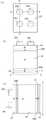
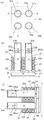
- FIGS. 5A to 5H A method of manufacturing the dynamic flash memory of this embodiment is shown using FIGS. 5A to 5H.
- (a) is a plan view
- (b) is a cross-sectional view along the XX' line of (a)
- (c) is a cross-sectional view along the YY' line of (a).
- 5F, and 5G (d) shows a cross-sectional view along line X1-X1'. Note that in an actual memory device, more than four dynamic flash memory cells are arranged in rows and columns on the substrate 10 .
- an N + layer 21, an N layer 25A, a P layer 22 made of Si, an N layer 25B, and an N + layer 23 are formed on a substrate 20 from the bottom. Then, mask material layers 24a, 24b, 24c, and 24d that are circular in plan view are formed.
- the substrate 20 may be formed of SOI (Silicon On Insulator), single-layered or multi-layered Si, or other semiconductor material. Also, the substrate 20 may be a well layer composed of a single layer of N layers or P layers, or a plurality of layers.
- the N layers 25A, 25B have a donor impurity concentration lower than that of the N + layers 21, 23 and higher than the acceptor impurity concentration of the P layer.
- the N + layer 23, the N layer 25B, the P layer 22, and the upper portion of the N layer 25A are etched to form the N + layer 21.
- the bottoms of the outer peripheral portions of the Si pillars 22a to 22d may be inside the N + layer 21.
- a SiO 2 layer 26 is formed on the N layer 25a around the Si pillars 22a to 22d.
- a gate insulating layer HfO 2 layer 27 is formed covering the entire surface by using ALD (Atomic Layer Deposition), for example.
- a TiN layer (not shown) serving as a gate conductor layer is formed to cover the entire surface.
- CMP Chemical Mechanical Polishing
- the HfO 2 layer 27 may be a single layer or other insulating layer consisting of multiple layers as long as it functions as a gate insulating layer. Also, as long as the TiN layer 28 has the function of a gate conductor layer, another conductor layer consisting of a single layer or multiple layers may be used.
- a SiO 2 layer 33 is formed on the TiN layer 28, as shown in FIG. 5D.
- the HfO 2 layer 27 above the SiO 2 layer 33 is etched to form an HfO 2 layer 27a.
- an HfO 2 layer 27b is formed over the entire surface.
- the entire surface is coated with a TiN layer (not shown) by the CVD method.
- the TiN layer is polished by the CMP method so that the upper surface position is the upper surface of the mask material layers 24a to 24d.
- etching is performed by the RIE method so that the upper surface positions are near the lower ends of the N layers 25ba to 25bd.
- a SiN layer 37a is formed to surround and connect side surfaces of the N layers 25ba and 25bb, the N + layers 23a and 23b, and the mask material layers 24a and 24b.
- a SiN layer 37b is formed surrounding and connecting the side surfaces of the N layers 25bc and 25bd, the N + layers 23c and 23d, and the mask material layers 24c and 24d.
- the TiN layer is etched to form TiN layers 36a and 36b.
- the length L1 between two intersections of the outer circumference of the HfO 2 layer 27b surrounding the Si pillars 22a and 22b and the line XX' is the length L1 of the SiN layers 37a and 37b along the line YY'.
- the length L3 between two intersections between the YY' line and the outer circumference of the HfO 2 layer 27b surrounding the Si pillars 22a and 22c is set to be larger than twice L2. .
- the SiN layer 37a can be connected between the Si pillars 22a and 22b and separated from the SiN layer 37b.
- the SiN layer 37b is connected between the Si pillars 22c and 22d and separated from the SiN layer 37a.
- holes 41aa, 41ab, 41ac, 41ba, 41bb, 41bc, 41ca, 41cb, and 41cc are formed between and around the sides of the TiN layers 36a, 36b and the SiN layers 37a, 37b. Then a SiO 2 layer 39 is formed. The upper end positions of the holes 41aa, 41ab, 41ac, 41ba, 41bb, 41bc, 41ca, 41cb, and 41cc are formed lower than the upper end positions of the TiN layers 36a and 36b indicated by dotted lines in FIG.
- the mask material layers 24a-24d are etched to form contact holes 40a, 40b, 40c and 40d.
- bit line BL1 conductor layer 42a connected to the N + layers 23a and 23c through the contact holes 40a and 40c, and the N + layer 23b through the contact holes 40b and 40d.
- a bit line BL2 conductor layer 42b connected to 23d is formed.
- a SiO 2 layer 43 containing holes 44a, 44b and 44c is formed between the bit line BL1 conductor layer 42a and the bit line BL2 conductor layer 42b and on both sides.
- a dynamic flash memory is thus formed on the substrate 20 .
- the TiN layers 36a and 36b serve as word line conductor layers WL1 and WL2, the TiN layer 28 serves as a plate line conductor layer PL also serving as a gate conductor layer, and the N + layer 21 serves as a source line conductor layer SL serving also as a source impurity layer. .
- a dynamic flash memory is thus formed on the substrate 20 .
- the dynamic flash memory device described in the description of the present embodiment satisfies the condition that the hole groups 11 generated by the impact ionization phenomenon or the gate-induced drain leakage current are retained in the channel region 7, the dynamic flash memory device has a structure that satisfies the condition. good.
- the channel region 7 may have a floating body structure separated from the substrate 1 .
- Non-Patent Document 11 GAA (Gate All Around: see, for example, Non-Patent Document 11) technology and Nanosheet technology (see, for example, Non-Patent Document 12), which is one of SGTs
- the semiconductor matrix in the channel region is formed into the substrate 1
- the dynamic flash memory operation described above is possible even if it is formed horizontally with respect to the
- it may be a device structure using SOI (Silicon On Insulator) (for example, see Non-Patent Documents 7 to 10).
- SOI Silicon On Insulator
- the bottom of the channel region is in contact with the insulating layer of the SOI substrate, and other channel regions are surrounded by a gate insulating layer and an element isolation insulating layer.
- the channel region has a floating body structure.
- the dynamic flash memory device provided by the present embodiment only needs to satisfy the condition that the channel region has a floating body structure. Also, even in a structure in which a Fin transistor (see, for example, Non-Patent Document 13) is formed on an SOI substrate, the dynamic flash memory operation can be performed if the channel region has a floating body structure.
- the length of the first gate conductor layer 5a connected to the plate line PL in the central axis direction is longer than the length of the first gate conductor layer 5b connected to the word line WL in the central axis direction. and C PL >C WL .
- the addition of the plate line PL alone reduces the capacitive coupling ratio (C WL /(C PL +C WL +C BL +C SL )) of the word line WL to the channel region 7 .
- the potential variation ⁇ V FB of the channel region 7 of the floating body becomes small.
- the voltage V ErasePL of the plate line PL may be a fixed voltage of 2 V, for example, regardless of each operation mode. Also, the voltage V ErasePL of the plate line PL may be applied, for example, 0 V only during erasing. Also, the voltage V ErasePL of the plate line PL may be a fixed voltage or a voltage that varies with time as long as it satisfies the conditions for dynamic flash memory operation.
- FIGS. 5A to 5H are described using the Si pillars 22a to 22d having rectangular vertical cross sections, these vertical cross sections may be trapezoidal. Further, the vertical cross sections of the Si pillars 22a to 22d in the portion surrounded by the HfO 2 layer 27a and the portion surrounded by the HfO 2 layer 27b may be rectangular or trapezoidal. These matters are the same in other embodiments according to the present invention.
- the potential distributions of the first channel region 7a and the second channel region 7b are formed to be connected. Thereby, the channel regions 7 of the first channel region 7a and the second channel region 7b are connected in the region surrounded by the insulating layer 6 in the vertical direction.
- the N + layer 21 also serves as a wiring conductor layer for the source line SL.
- a conductor layer such as a W layer formed between the N + layers 21 at the bottoms of the Si pillars 22a to 22d may be used as the source line SL.
- a conductor layer made of a metal such as a W layer or an alloy may be formed on the N + layer 11 outside the region where more Si pillars 22a to 22d are formed two-dimensionally.
- the voltage of the word line WL of the plate line PL of the dynamic flash memory cell according to the first embodiment of the present invention fluctuates up and down when the dynamic flash memory cell performs write and read operations.
- the plate line PL serves to reduce the capacitive coupling ratio between the word line WL and the channel region 7 .
- the influence of the voltage change in the channel region 7 when the voltage of the word line WL swings up and down can be significantly suppressed.
- the threshold voltage difference indicating logic "0" and "1” can be increased. This leads to increased operating margins for dynamic flash memory cells.
- the N layers 8a and 8b in FIG. 1 are affected by the voltage applied to the source line SL, the plate line PL, the word line WL, and the bit line BL, or by capacitive coupling noise with peripheral memory cells. As a result, unnecessary electrons are suppressed from flowing into the channel region 7 from one or both of the N + layer 3a connected to the word line WL and the N + layer 3b connected to the bit line BL. This allows the dynamic flash memory to operate stably, leading to higher performance.
- the N layer 25a shown in FIG. 5H has a role of suppressing the flow of unnecessary electrons from the N + layer 21 into the Si pillars 22a to 22d, and the source or drain of the SGT transistor using the Si pillars 22a to 22d as channels. perform the role of The N + layer 21 also serves as a low-resistance connection electrode for the N layer 25a, which is the source or drain.
- the N layer 25a and the N + layer 21 are located under the Si pillars 22a-22d and over the entire surface of the substrate 20.
- the N + layer 21 is connected to the metal or alloy conductor layer in the region outside the Si pillars 22a-22d. Since the N + layer 21 is present on the entire surface of the substrate 20, the source line SL voltage can be applied more uniformly to the N layer 25a under the Si pillars 22a to 22d. This allows the dynamic flash memory to operate stably, leading to higher performance.
- the N layer 8a is formed by voltages applied to the source line SL, plate line PL, word line WL, and bit line BL of the dynamic flash memory, or by capacitive coupling with peripheral memory cells. This suppresses unwanted electrons from flowing into the channel region 7 from the N + layer 3a connected to the source line SL under the influence of noise. Since N layer 8b in FIG. 1, which acts as a series resistance, is not present between N + layer 3b and channel region 7, the speed of the dynamic flash memory can be increased. In this way, the dynamic flash memory can operate stably and achieve high performance. (Feature 2) Further, even if the N layer 8a is eliminated and the N layer 8b in FIG.
- the dynamic flash memory can operate stably and improve performance.
- the Si pillars 2, 22a to 22d are formed in the above embodiment, the semiconductor pillars may be made of a semiconductor material other than Si. This also applies to other embodiments according to the present invention.
- the N + layers 3a, 3b, 21, 23 in the first embodiment may be formed of Si containing donor impurities or other semiconductor material layers.
- the N + layers 3a, 3b, 21, 23 may be formed from different semiconductor material layers.
- the N + layer may be formed by an epitaxial crystal growth method or another method.
- the N layers 25a, 25ba, 25bb, 25bc, and 25bd may also be formed of Si containing donor impurities or other semiconductor material layers.
- the N layer may be formed by an epitaxial crystal growth method or another method. This also applies to other embodiments according to the present invention.
- the TiN layer 28 is used as the plate line PL and the gate conductor layer 5a connected to the plate line PL.
- a single layer or a combination of multiple conductor material layers may be used instead of the TiN layer 28 .
- TiN layers 36a and 36b were used as the word line WL and the gate conductor layer 5b connected to the word line WL.
- the gate TiN layer may be connected to a wiring metal layer such as W on the outside thereof. This also applies to other embodiments according to the present invention.
- the shape of the Si pillars 22a to 22d viewed from the central axis direction was circular, but may be circular, elliptical, or elongated in one direction.
- Si pillars having different plan view shapes can be mixed and formed in the logic circuit area according to the logic circuit design.
- the Si pillar 2 having a rectangular vertical cross section was used for the description, but the vertical cross-sectional shape may be trapezoidal.
- the vertical cross sections of the Si pillar 2 of the portion surrounded by the first gate insulating layer 4a and the portion surrounded by the second gate insulating layer 4b may be rectangular, trapezoidal, or the like. .
- the source line SL is negatively biased during the erasing operation to pull out the group of holes in the channel region 7 which is the floating body FB. may be negatively biased, or the source line SL and the bit line BL may be negatively biased to perform the erase operation. Alternatively, the erase operation may be performed under other voltage conditions. This also applies to other embodiments according to the present invention.
- the N layers 25a, 25ba-25bd were formed by epitaxial growth.
- the N layers 25a, 25ba to 25bd may be formed by ion implantation.
- the N layers 25a, 25ba to 25bd may be formed by diffusing donor impurities from the N + layers 21, 23a to 23d by heat treatment.
Landscapes
- Engineering & Computer Science (AREA)
- Microelectronics & Electronic Packaging (AREA)
- Computer Hardware Design (AREA)
- Manufacturing & Machinery (AREA)
- Semiconductor Memories (AREA)
- Non-Volatile Memory (AREA)
- Thin Film Transistor (AREA)
- Dram (AREA)
Abstract
基板1上に、垂直方向に立つSi柱2の両端にあるソース線SLに繋がるN+層3aと、ビット線BLに繋がるN+層3bと、N+層3aに繋がるN層8aと、N+層3bに繋がるN層8bと、Si柱2を囲んだ第1のゲート絶縁層4aと、第1のゲート絶縁層4aを囲みプレート線PLに繋がる第1のゲート導体層5aと、Si柱2を囲んだゲート絶縁層4bを囲んだワード線WLに繋がる第2のゲート導体層5bがあり、ソース線SL、プレート線PL、ワード線WL、ビット線BLに印加する電圧を制御して、Si柱2のチャネル領域7の内部でインパクトイオン現象、またはゲート誘起ドレインリーク電流により発生した正孔群を保持するデータ保持動作と、そして、この正孔群を、チャネル領域7内から除去するデータ消去動作を行う。
Description
本発明は、半導体素子を用いたメモリ装置。
近年、LSI(Large Scale Integration)技術開発において、メモリ素子の高集積化と高性能化が求められている。
通常のプレナー型MOSトランジスタでは、チャネルが半導体基板の上表面に沿う水平方向に延在する。これに対して、SGTのチャネルは、半導体基板の上表面に対して垂直な方向に延在する(例えば、特許文献1、非特許文献1を参照)。このため、SGTはプレナー型MOSトランジスタと比べ、半導体装置の高密度化が可能である。このSGTを選択トランジスタとして用いて、キャパシタを接続したDRAM(Dynamic Random Access Memory、例えば、非特許文献2を参照)、抵抗変化素子を接続したPCM(Phase Change Memory、例えば、非特許文献3を参照)、RRAM(Resistive Random Access Memory、例えば、非特許文献4を参照)、電流により磁気スピンの向きを変化させて抵抗を変化させるMRAM(Magneto-resistive Random Access Memory、例えば、非特許文献5を参照)などの高集積化を行うことができる。また、キャパシタを有しない、1個のMOSトランジスタで構成された、DRAMメモリセル(非特許文献6を参照)などがある。本願は、抵抗変化素子やキャパシタを有しない、MOSトランジスタのみで構成可能な、ダイナミック フラッシュ メモリに関する。
図7に、前述したキャパシタを有しない、1個のMOSトランジスタで構成された、DRAMメモリセルの書込み動作と、図8に、動作上の問題点と、図9に、読出し動作を示す(非特許文献7~10を参照)。
図7にDRAMメモリセルの書込み動作を示す。図7(a)は、“1”書込み状態を示している。ここで、メモリセルは、SOI基板101に形成され、ソース線SLが接続されるソースN+層103(以下、ドナー不純物を高濃度で含む半導体領域を「N+層」と称する。)、ビット線BLが接続されるドレインN+層104、ワード線WLが接続されるゲート導電層105、MOSトランジスタ110aのフローティングボディ(Floating Body)102により構成され、キャパシタを有さず、MOSトランジスタ110aが1個でDRAMのメモリセルが構成されている。なお、フローティングボディ102直下には、SOI基板のSiO2層101が接している。このMOSトランジスタ110a、1個で構成されたメモリセルの“1”書込みを行う際には、MOSトランジスタ110aを線形領域で動作させる。すなわち、ソースN+層103から延びる電子のチャネル107には、ピンチオフ点108があり、ビット線が接続しているドレインN+層104までには、到達していない。このようにドレインN+層104に接続されたビット線BLとゲート導電層105に接続されたワード線WLを共に高電圧にして、ゲート電圧をドレイン電圧の約1/2程度で、MOSトランジスタ110aを動作させると、ドレインN+層104近傍のピンチオフ点108において、電界強度が最大となる。この結果、ソースN+層103からドレインN+層104に向かって流れる加速された電子は、Siの格子に衝突して、その時に失う運動エネルギーによって、電子・正孔対が生成される(インパクトイオン化現象)。発生した大部分の電子(図示せず)は、ドレインN+層104に到達する。また、ごく一部のとても熱い電子は、ゲート酸化膜109を飛び越えて、ゲート導電層105に到達する。そして、同時に発生した正孔106は、フローティングボディ102を充電する。この場合、発生した正孔は、フローティングボディ102がP型Siのため、多数キャリアの増分として、寄与する。フローティングボディ102は、生成された正孔106で満たされ、フローティングボディ102の電圧がソースN+層103よりもVb以上に高くなると、さらに生成された正孔は、ソースN+層103に放電する。ここで、Vbは、ソースN+層103とP層のフローティングボディ102との間のPN接合のビルトイン電圧であり、約0.7Vである。図7(b)には、生成された正孔106でフローティングボディ102が飽和充電された様子を示している。
次に、図7(c)を用いて、メモリセル110の“0”書込み動作を説明する。共通な選択ワード線WLに対して、ランダムに“1”書込みのメモリセル110aと“0”書込みのメモリセル110bが存在する。図7(c)では、“1”書込み状態から“0”書込み状態に書き換わる様子を示している。“0”書込み時には、ビット線BLの電圧を負バイアスにして、ドレインN+層104とP層のフローティングボディ102との間のPN接合を順バイアスにする。この結果、フローティングボディ102に予め前サイクルで生成された正孔106は、ビット線BLに接続されたドレインN+層104に流れる。書込み動作が終了すると、生成された正孔106で満たされたメモリセル110a(図7(b))と、生成された正孔が吐き出されたメモリセル110b(図7(c))の2つのメモリセルの状態が得られる。正孔106で満たされたメモリセル110aのフローティングボディ102の電位は、生成された正孔がいないフローティングボディ102よりも高くなる。したがって、メモリセル110aのしきい値電圧は、メモリセル110bのしきい値電圧よりも低くなる。その様子を図7(d)に示す。
次に、この1個のMOSトランジスタで構成されたメモリセルの動作上の問題点を図8を用いて、説明する。図8(a)に示したように、フローティングボディ102の容量CFBは、ワード線の接続されたゲートとフローティングボディ102間の容量CWLと、ソース線の接続されたソースN+層103とフローティングボディ102との間のPN接合の接合容量CSLと、ビット線の接続されたドレインN+層103とフローティングボディ102との間のPN接合の接合容量CBLとの総和で、
CFB = CWL + CBL + CSL (1)
で表される。したがって、書込み時にワード線電圧VWLが振幅すると、メモリセルの記憶ノード(接点)となるフローティングボディ102の電圧も、その影響を受ける。その様子を図8(b)に示している。書込み時にワード線電圧VWLが0VからVProgWLに上昇すると、フローティングボディ102の電圧VFBは、ワード線電圧が変化する前の初期状態の電圧VFB1からVFB2へのワード線との容量結合によって上昇する。その電圧変化量ΔVFBは、
ΔVFB = VFB2 - VFB1
= CWL / (CWL + CBL + CSL) × VProgWL (2)
で表される。
ここで、
β= CWL / (CWL + CBL + CSL) (3)
で表され、βをカップリング率と呼ぶ。このようなメモリセルにおいて、CWLの寄与率が大きく、例えば、CWL:CBL:CSL=8:1:1である。この場合、β=0.8となる。ワード線が、例えば、書込み時の5Vから、書込み終了後に0Vになると、ワード線とフローティングボディ102との容量結合によって、フローティングボディ102が、5V×β=4Vも振幅ノイズを受ける。このため、書込み時のフローティングボディ“1”電位と“0”電位との電位差マージンを十分に取れない問題点があった。
CFB = CWL + CBL + CSL (1)
で表される。したがって、書込み時にワード線電圧VWLが振幅すると、メモリセルの記憶ノード(接点)となるフローティングボディ102の電圧も、その影響を受ける。その様子を図8(b)に示している。書込み時にワード線電圧VWLが0VからVProgWLに上昇すると、フローティングボディ102の電圧VFBは、ワード線電圧が変化する前の初期状態の電圧VFB1からVFB2へのワード線との容量結合によって上昇する。その電圧変化量ΔVFBは、
ΔVFB = VFB2 - VFB1
= CWL / (CWL + CBL + CSL) × VProgWL (2)
で表される。
ここで、
β= CWL / (CWL + CBL + CSL) (3)
で表され、βをカップリング率と呼ぶ。このようなメモリセルにおいて、CWLの寄与率が大きく、例えば、CWL:CBL:CSL=8:1:1である。この場合、β=0.8となる。ワード線が、例えば、書込み時の5Vから、書込み終了後に0Vになると、ワード線とフローティングボディ102との容量結合によって、フローティングボディ102が、5V×β=4Vも振幅ノイズを受ける。このため、書込み時のフローティングボディ“1”電位と“0”電位との電位差マージンを十分に取れない問題点があった。
図9に読出し動作を示す。図9(a)は、“1”書込み状態を、図9(b)は、“0”書込み状態を示している。しかし、実際には、“1”書込みでフローティングボディ102にVbが書き込まれていても、書込み終了でワード線が0Vに戻ると、フローティングボディ102は、負バイアスに引き下げられる。“0”が書かれる際には、さらに深く負バイアスになってしまうため、図9(c)に示すように、書込みの際に“1”と“0”との電位差マージンを十分に大きく出来ない。この動作マージンが小さいことが、本DRAMメモリセルの大きい問題であった。加えて、このDRAMメモリセルを高密度化する課題がある。
Hiroshi Takato, Kazumasa Sunouchi, Naoko Okabe, Akihiro Nitayama, Katsuhiko Hieda, Fumio Horiguchi, and Fujio Masuoka: IEEE Transaction on Electron Devices, Vol.38, No.3, pp.573-578 (1991)
H. Chung, H. Kim, H. Kim, K. Kim, S. Kim, K. Dong, J. Kim, Y.C. Oh, Y. Hwang, H. Hong, G. Jin, and C. Chung: "4F2 DRAM Cell with Vertical Pillar Transistor(VPT)," 2011 Proceeding of the European Solid-State Device Research Conference, (2011)
H. S. Philip Wong, S. Raoux, S. Kim, Jiale Liang, J. R. Reifenberg, B. Rajendran, M. Asheghi and K. E. Goodson: "Phase Change Memory," Proceeding of IEEE, Vol.98, No 12, December, pp.2201-2227 (2010)
T. Tsunoda, K .Kinoshita, H. Noshiro, Y. Yamazaki, T. Iizuka, Y. Ito, A. Takahashi, A. Okano, Y. Sato, T. Fukano, M. Aoki, and Y. Sugiyama : "Low Power and high Speed Switching of Ti-doped NiO ReRAM under the Unipolar Voltage Source of less than 3V," IEDM (2007)
W. Kang, L. Zhang, J. Klein, Y. Zhang, D. Ravelosona, and W. Zhao: "Reconfigurable Codesign of STT-MRAM Under Process Variations in Deeply Scaled Technology," IEEE Transaction on Electron Devices, pp.1-9 (2015)
M. G. Ertosum, K. Lim, C. Park, J. Oh, P. Kirsch, and K. C. Saraswat : "Novel Capacitorless Single-Transistor Charge-Trap DRAM (1T CT DRAM) Utilizing Electron," IEEE Electron Device Letter, Vol. 31, No.5, pp.405-407 (2010)
J. Wan, L. Rojer, A. Zaslavsky, and S. Critoloveanu: "A Compact Capacitor-Less High-Speed DRAM Using Field Effect-Controlled Charge Regeneration," Electron Device Letters, Vol. 35, No.2, pp.179-181 (2012)
T. Ohsawa, K. Fujita, T. Higashi, Y. Iwata, T. Kajiyama, Y. Asao, and K. Sunouchi: "Memory design using a one-transistor gain cell on SOI," IEEE JSSC, vol.37, No.11, pp1510-1522 (2002).
T. Shino, N. Kusunoki, T. Higashi, T. Ohsawa, K. Fujita, K. Hatsuda, N. Ikumi, F. Matsuoka, Y. Kajitani, R. Fukuda, Y. Watanabe, Y. Minami, A. Sakamoto, J. Nishimura, H. Nakajima, M. Morikado, K. Inoh, T. Hamamoto, A. Nitayama: "Floating Body RAM Technology and its Scalability to 32nm Node and Beyond," IEEE IEDM (2006).
E. Yoshida: "A Capacitorless 1T-DRAM Technology Using Gate-Induced Drain-Leakage (GIDL) Current for Low-Power and High-Speed Embedded Memory," IEEE IEDM (2006).
J. Y. Song, W. Y. Choi, J. H. Park, J. D. Lee, and B-G. Park: "Design Optimization of Gate-All-Around (GAA) MOSFETs," IEEE Trans. Electron Devices, vol. 5, no. 3, pp.186-191, May 2006.
N. Loubet, et al.: "Stacked Nanosheet Gate-All-Around Transistor to Enable Scaling Beyond FinFET," 2017 IEEE Symposium on VLSI Technology Digest of Technical Papers, T17-5, T230-T231, June 2017.
H. Jiang, N. Xu, B. Chen, L. Zeng1, Y. He, G. Du, X. Liu and X. Zhang: "Experimental investigation of self heating effect (SHE) in multiple-fin SOI FinFETs," Semicond. Sci. Technol. 29 (2014) 115021 (7pp).
E. Yoshida, and T. Tanaka: "A Capacitorless 1T-DRAM Technology Using Gate-Induced Drain-Leakage (GIDL) Current for Low-Power and High-Speed Embedded Memory," IEEE Transactions on Electron Devices, Vol. 53, No. 4, pp. 692-697,Apr. 2006.
SGTを用いたメモリ装置でキャパシタを無くした、1個のトランジス型のDRAM(ゲインセル)では、ワード線とフローティング状態のSGTのボディとの容量結合カップリングが大きく、データ読み出し時や書き込み時にワード線の電位を振幅させると、直接SGTボディへのノイズとして、伝達されてしまう問題点があった。この結果、誤読み出しや記憶データの誤った書き換えの問題を引き起こし、キャパシタを無くした1トランジス型のDRAM(ゲインセル)の実用化が困難となっていた。そして、上記問題を解決すると共に、DRAMメモリセルを高密度化する必要がある。
上記の課題を解決するために、本発明に係るメモリ装置は、
基板上に、前記基板に対して、垂直方向に立つか、または水平方向に伸延する半導体母体と、
前記半導体母体の一端側の側面の一部、または全てを囲んだ第1のゲート絶縁層と、
前記第1のゲート絶縁層に繋がり、且つ前記半導体母体の他端側の側面の一部、または全てを囲んだ第2のゲート絶縁層と、
前記第1のゲート絶縁層を覆った第1のゲート導体層と、
前記第2のゲート絶縁層を覆った第2のゲート導体層と、
前記半導体母体が伸延する方向において、前記第1のゲート導体層の一端の外側にある第1の不純物層と、前記第2のゲート導体層の一端の外側にある第2の不純物層と、
前記第1の不純物層と前記第2の不純物層の、一方または両方と、前記半導体母体との間にあり、且つ前記第1の不純物層及び前記第2の不純物層と同じ導電型を有する第3の不純物層と、
前記第1の不純物層に接続した第1の配線導体層と、
前記第2の不純物層に接続した第2の配線導体層と、
前記第1のゲート導体層に接続した第3の配線導体層と、
前記第2のゲート導体層に接続した第4の配線導体層と、を有し、
前記第1の配線導体層と、前記2の配線導体層と、前記3の配線導体層と、前記4の配線導体層と、に印加する電圧を制御して、前記第1の不純物層と前記第2の不純物層との間に流す電流でインパクトイオン化現象、またはゲート誘起ドレインリーク電流により電子群と正孔群を前記半導体母体内に発生させる動作と、発生させた前記電子群と前記正孔群の内、前記半導体母体における少数キャリアである前記電子群と前記正孔群のいずれかを除去する動作と、前記半導体母体における多数キャリアである前記電子群と前記正孔群のいずれかの一部または全てを、前記半導体母体に残存させる動作と、を行ってメモリ書き込み動作を行い、
前記第1の配線導体層と、前記第2の配線導体層と、前記第3の配線導体層と、前記第4の配線導体層とに印加する電圧を制御して、前記第1の不純物層と、前記第2の不純物層の一方もしくは両方から、残存している前記半導体母体における多数キャリアである前記電子群と前記正孔群のいずれかを抜き取り、メモリ消去動作を行う、
ことを特徴とする(第1発明)。
基板上に、前記基板に対して、垂直方向に立つか、または水平方向に伸延する半導体母体と、
前記半導体母体の一端側の側面の一部、または全てを囲んだ第1のゲート絶縁層と、
前記第1のゲート絶縁層に繋がり、且つ前記半導体母体の他端側の側面の一部、または全てを囲んだ第2のゲート絶縁層と、
前記第1のゲート絶縁層を覆った第1のゲート導体層と、
前記第2のゲート絶縁層を覆った第2のゲート導体層と、
前記半導体母体が伸延する方向において、前記第1のゲート導体層の一端の外側にある第1の不純物層と、前記第2のゲート導体層の一端の外側にある第2の不純物層と、
前記第1の不純物層と前記第2の不純物層の、一方または両方と、前記半導体母体との間にあり、且つ前記第1の不純物層及び前記第2の不純物層と同じ導電型を有する第3の不純物層と、
前記第1の不純物層に接続した第1の配線導体層と、
前記第2の不純物層に接続した第2の配線導体層と、
前記第1のゲート導体層に接続した第3の配線導体層と、
前記第2のゲート導体層に接続した第4の配線導体層と、を有し、
前記第1の配線導体層と、前記2の配線導体層と、前記3の配線導体層と、前記4の配線導体層と、に印加する電圧を制御して、前記第1の不純物層と前記第2の不純物層との間に流す電流でインパクトイオン化現象、またはゲート誘起ドレインリーク電流により電子群と正孔群を前記半導体母体内に発生させる動作と、発生させた前記電子群と前記正孔群の内、前記半導体母体における少数キャリアである前記電子群と前記正孔群のいずれかを除去する動作と、前記半導体母体における多数キャリアである前記電子群と前記正孔群のいずれかの一部または全てを、前記半導体母体に残存させる動作と、を行ってメモリ書き込み動作を行い、
前記第1の配線導体層と、前記第2の配線導体層と、前記第3の配線導体層と、前記第4の配線導体層とに印加する電圧を制御して、前記第1の不純物層と、前記第2の不純物層の一方もしくは両方から、残存している前記半導体母体における多数キャリアである前記電子群と前記正孔群のいずれかを抜き取り、メモリ消去動作を行う、
ことを特徴とする(第1発明)。
上記の第1発明において、前記第3の不純物層の不純物濃度が、前記第1の不純物層と前記第2の不純物層の不純物濃度より低く、且つ前記半導体母体の不純物濃度より大きいことを特徴とする(第2発明)。
上記の第1発明において、前記第1の不純物層に繋がる配線は、ソース線であり、前記第2の不純物層に繋がる配線はビット線であり、前記第1のゲート導体層に繋がる配線は、第1の駆動制御線であり、前記第2のゲート導体層に繋がる配線はワード線であり、前記ソース線と、前記ビット線と、前記第1の駆動制御線と、前記ワード線とに印加する電圧により、前記メモリ消去動作と、前記メモリ書き込み動作と、を行うことを特徴とする(第3発明)。
上記の第2発明において、前記ビット線に接続する前記第2の不純物層に繋がる位置に前記第3の不純物層が形成されていることを特徴とする(第4発明)。
上記の第2発明において、前記ソース線に接続する前記第1の不純物層に繋がる位置に前記第3の不純物層が形成されていることを特徴とする(第5発明)。
上記の第2発明において、前記ソース線に接続する前記第1の不純物層に繋がる位置と、前記ビット線に接続するに繋がる位置と、の両者に前記第3の不純物層が形成されていることを特徴とする(第6発明)。
上記の第1発明において、前記第1のゲート導体層と前記半導体母体との間の第1のゲート容量は、前記第2のゲート導体層と前記半導体母体との間の第2のゲート容量よりも大きいことを特徴とする(第7発明)。
上記の第1発明において、前記半導体母体が、前記基板に対し垂直方向に立ち、且つ、平面視において、前記第1の不純物層と、前記半導体母体に繋がる前記第3の不純物層とが、前記半導体母体の外側に広がっていることを特徴とする(第8発明)。
以下、本発明に係る、半導体素子を用いたメモリ装置(以後、ダイナミック フラッシュ メモリと呼ぶ)の構造、駆動方式、製造方法について、図面を参照しながら説明する。
(第1実施形態)
図1~図5を用いて、本発明の第1実施形態に係るダイナミック フラッシュ メモリセルの構造と動作メカニズムと製造方法とを説明する。図1を用いて、ダイナミック フラッシュ メモリセルの構造を説明する。そして、図2を用いてデータ消去メカニズムを、図3を用いてデータ書き込みメカニズムを、図4を用いてデータ書き込みメカニズムを説明する。図5を用いて、ダイナミック フラッシュ メモリの製造方法を説明する。
図1~図5を用いて、本発明の第1実施形態に係るダイナミック フラッシュ メモリセルの構造と動作メカニズムと製造方法とを説明する。図1を用いて、ダイナミック フラッシュ メモリセルの構造を説明する。そして、図2を用いてデータ消去メカニズムを、図3を用いてデータ書き込みメカニズムを、図4を用いてデータ書き込みメカニズムを説明する。図5を用いて、ダイナミック フラッシュ メモリの製造方法を説明する。
図1に、本発明の第1実施形態に係るダイナミック フラッシュ メモリセルの構造を示す。基板1(特許請求の範囲の「基板」の一例である)上にN+層3a(特許請求の範囲の「第1の不純物層」の一例である)がある。そして、N+層3a上に、アクセプタ不純物を含むP型又はi型(真性型)の導電型を有するシリコン半導体柱2(特許請求の範囲の「半導体母体」の一例である)(以下、シリコン半導体柱を「Si柱」と称する。)がある。このSi柱2の底部にN層8a(特許請求の範囲の「第3の不純物層」の一例である)、頂部にN層8b(特許請求の範囲の「第3の不純物層」の一例である)がある。そして、N層8bの上にN+層3b(特許請求の範囲の「第2の不純物層」の一例である)がある。N層8a、8bのドナー不純物濃度はN+層3a、3bよりも低い。N層8a、8b間のSi柱2の部分がチャネル領域7となる。このチャネル領域7を囲むように、下より第1のゲート絶縁層4a(特許請求の範囲の「第1のゲート絶縁層」の一例である)と、第2のゲート絶縁層4b(特許請求の範囲の「第2のゲート絶縁層」の一例である)とがある。この第1のゲート絶縁層4a、第2のゲート絶縁層4bは、N層8a、8bに、それぞれ接するか、または近接している。この第1のゲート絶縁層4aを囲んで第1のゲート導体層5a(特許請求の範囲の「第1のゲート導体層」の一例である)があり、第2のゲート絶縁層4bを囲んで、第2のゲート導体層5b(特許請求の範囲の「第2のゲート導体層」の一例である)がある。そして、第1のゲート導体層5a、第2のゲート導体層5bは絶縁層6により分離されている。N層8a、8b間のSi柱2の部分であるチャネル領域7は、第1のゲート絶縁層4aで囲まれた第1のチャネル領域7aと、第2のゲート絶縁層4bで囲まれた第2のチャネル領域7bと、よりなる。これによりN+層3a、3b、N層層8a、8b、チャネル領域7、第1のゲート絶縁層4a、第2のゲート絶縁層4b、第1のゲート導体層5a、第2のゲート導体層5bからなるダイナミック フラッシュ メモリセルが形成される。そして、N+層3aはソース線SL(特許請求の範囲の「ソース線」の一例である)に、N+層3bはビット線BL(特許請求の範囲の「ビット線」の一例である)に、第1のゲート導体層5aはプレート線PL(特許請求の範囲の「第1の駆動制御線」の一例である)に、第2のゲート導体層5bはワード線WL(特許請求の範囲の「ワード線」の一例である)に、それぞれ接続している。N層8a、8bは、ダイナミック フラッシュ メモリが、ソース線SL、プレート線PL、ワード線WL、ビット線BLに印加される電圧によって、不要な電子がソース線SLに繋がるN+層3aと、ビット線BLに繋がるN+層3bよりチャネル領域7に流入することを抑圧している。プレート線PLに接続している、第1のゲート導体層5aのゲート容量は、ワード線WLに接続している、第2のゲート導体層5bのゲート容量よりも、大きくなるような構造を有することが望ましい。メモリ装置では、上述の複数のダイナミック フラッシュ メモリセルが基板1上に2次元状に配置されている。
なお、図1では、プレート線PLに接続された第1のゲート導体層5aのゲート容量が、ワード線WLが接続された、第2のゲート導体層5bのゲート容量よりも、大きくなるように第1のゲート導体層5aのゲート長を、第2のゲート導体層5bのゲート長よりも長くしている。しかし、その他にも、第1のゲート導体層5aのゲート長を、第2のゲート導体層5bのゲート長よりも長くせずに、第1のゲート絶縁層4aのゲート絶縁膜の膜厚を、第2のゲート絶縁層4bのゲート絶縁膜の膜厚よりも薄くしてもよい。また、第1のゲート絶縁層4aの誘電率を、第2のゲート絶縁層4bの誘電率よりも高くしてもよい。また、ゲート導体層5a、5bの長さ、ゲート絶縁層4a、4bの膜厚、誘電率のいずれかを組み合わせて、第1のゲート導体層5aのゲート容量が、第2のゲート導体層5bのゲート容量よりも、大きくしてもよい。
また、垂直方向において、N層8aの上端位置は、第1のゲート導体層5aの下端位置より上方にあっても、また下方にあってもよい。同じく、N層8bの下端位置は、第2のゲート導体層5bの上端位置より上方にあっても、また下方にあってもよい。
また、第1のゲート導体層5aは2つ以上に分割して、それぞれをプレート線の導体電極として、同期または非同期で動作させてもよい。同様に、第2のゲート導体層5bは2つ以上に分割して、それぞれをワード線の導体電極として、同期または非同期で動作させてもよい。これによっても、ダイナミック フラッシュ メモリ動作がなされる。
また、N+層3a、3b、N層8a、8b、P型のSi柱2のそれぞれの導電性の極性を逆にした構造においても、ダイナミック フラッシュ メモリ動作がなされる。この場合、N型のSi柱では、多数キャリアは電子になる。従って、インパクトイオン化により生成された電子群がチャネル領域7に蓄えられて、“1”状態が設定される。
図2に、消去動作メカニズムを説明する。N層8a、8b間のチャネル領域7は、電気的に基板から分離され、フローティングボディとなっている。図2(a)に消去動作前に、前のサイクルでインパクトイオン化により生成された正孔群11がチャネル領域7に蓄えられている状態を示す。そして。図2(b)に示すように、消去動作時には、ビット線BLの電圧を、負電圧VERAにする。ここで、VERAは、例えば、-3Vである。その結果、チャネル領域7の初期電位の値に関係なく、ソース線SLが接続されているソースとなるN+層3a、N層8aとチャネル領域7のPN接合が順バイアスとなる。その結果、前のサイクルでインパクトイオン化により生成された、チャネル領域7に蓄えられていた、正孔群11が、ソース部のN+層3a、N層8aに吸い込まれ、チャネル領域7の電位VFBは、VFB=VERA+Vbとなる。ここで、VbはPN接合のビルトイン電圧であり、約0.7Vである。したがって、VERA=-3Vの場合、チャネル領域7の電位は、-2.3Vになる。この値が、消去状態のチャネル領域7の電位状態となる。このため、フローティングボディのチャネル領域7の電位が負の電圧になると、ダイナミック フラッシュ メモリセル9のNチャネルMOSトランジスタのしきい値電圧は、基板バイアス効果によって、高くなる。これにより、図2(c)に示すように、このワード線WLが接続された第2のゲート導体層5bのしきい値電圧は高くなる。このチャネル領域7の消去状態は論理記憶データ“0”となる。なお、上記のビット線BL、ソース線SL、ワード線WL、プレート線PLに印加する電圧条件は、消去動作を行うための一例であり、消去動作ができる他の動作条件であってもよい。
図3に、本発明の第1実施形態に係るダイナミック フラッシュ メモリセルの書込み動作を示す。図3(a)に示すように、ソース線SLの接続されたN+層3aに例えば0Vを入力し、ビット線BLの接続されたN+層3bに例えば3Vを入力し、プレート線PLの接続された第1のゲート導体層5aに、例えば、2Vを入力し、ワード線WLの接続された第2のゲート導体層5bに、例えば、5Vを入力する。その結果、図3(a)で示したように、プレート線PLの接続された第1のゲート導体層5aの内側の第1のチャネル領域7aには、環状の反転層12aが形成され、第1のゲート導体層5aを有する第1のNチャネルMOSトランジスタは線形領域で動作させる。この結果、プレート線PLの接続された第1のゲート導体層5aの内側の反転層12aには、ピンチオフ点13が存在する。一方、ワード線WLの接続された第2のゲート導体層5bを有する第2のNチャネルMOSトランジスタは飽和領域で動作させる。この結果、ワード線WLの接続された第2のゲート導体層5bの内側の第2のチャネル領域7bには、ピンチオフ点は存在せずに全面に反転層12bが形成される。このワード線WLの接続された第2のゲート導体層5bの内側に全面に形成された反転層12bは、第2のゲート導体層5bを有する第2のNチャネルMOSトランジスタの実質的なドレインとして働く。この結果、直列接続された第1のゲート導体層5aを有する第1のNチャネルMOSトランジスタと、第2のゲート導体層5bを有する第2のNチャネルMOSトランジスタとの間のチャネル領域7の第1の境界領域で電界は最大となり、この領域でインパクトイオン化現象が生じる。この領域は、ワード線WLの接続された第2のゲート導体層5bを有する第2のNチャネルMOSトランジスタから見たソース側の領域であるため、この現象をソース側インパクトイオン化現象と呼ぶ。このソース側インパクトイオン化現象により、ソース線SLの接続されたN+層3a、N層8aからビット線BLの接続されたN+層3b、N層8bに向かって電子が流れる。加速された電子が格子Si原子に衝突し、その運動エネルギーによって、電子・正孔対が生成される。生成された電子の一部は、第1のゲート導体層5aと第2のゲート導体層5bに流れるが、大半はビット線BLの接続されたN+層3bに流れる。また、“1”書込みにおいて、ゲート誘起ドレインリーク(GIDL:Gate Induced Drain Leakage)電流を用いて電子・正孔対を発生させ、生成された正孔群でフローティングボディFB内を満たしてもよい(非特許文献14を参照)。なお、インパクトイオン化現象による電子・正孔対の生成は、N層8aとチャネル領域7の境界、またはN層8bとチャネル領域7との境界でも行うことが出来る。
そして、図3(b)に示すように、生成された正孔群11は、チャネル領域7の多数キャリアであり、チャネル領域7を正バイアスに充電する。ソース線SLの接続されたN+層3aは、0Vであるため、チャネル領域7はソース線SLの接続されたN+層3a、N層8aとチャネル領域7との間のPN接合のビルトイン電圧Vb(約0.7V)まで充電される。チャネル領域7が正バイアスに充電されると、第1のNチャネルMOSトランジスタと第2のNチャネルMOSトランジスタのしきい値電圧は、基板バイアス効果によって、低くなる。これにより、図3(c)で示すように、ワード線WLの接続された第2のチャネル領域7bのNチャネルMOSトランジスタのしきい値電圧は、低くなる。このチャネル領域7の書込み状態を論理記憶データ“1”に割り当てる。
なお、書込み動作時に、上記の第1の境界領域に替えて、N層8aと第1のチャネル半導体層7aとの間の第2の境界領域、または、N層8bと第2のチャネル半導体層7bとの間の第3の境界領域で、インパクトイオン化現象、またはGIDL電流で、電子・正孔対を発生させ、発生した正孔群11でチャネル領域7を充電しても良い。なお、上記のビット線BL、ソース線SL、ワード線WL、プレート線PLに印加する電圧条件は、書き込み動作を行うための一例であり、書き込み動作ができる他の動作条件であってもよい。
図4A、図4Bを用いて、本発明の第1実施形態に係るダイナミック フラッシュ メモリセルの読出し動作を説明する。図4A(a)~図4A(c)を用いて、ダイナミック フラッシュ メモリセルの読出し動作を説明する。図4A(a)に示すように、チャネル領域7がビルトイン電圧Vb(約0.7V)まで充電されると、NチャネルMOSトランジスタのしきい値電圧が基板バイアス効果によって、低下する。この状態を論理記憶データ“1”に割り当てる。図4A(b)に示すように、書込みを行う前に選択するメモリブロックは、予め消去状態“0”にある場合は、チャネル領域7のフローティング電圧VFBはVERA+Vbとなっている。書込み動作によってランダムに書込み状態“1”が記憶される。この結果、ワード線WLに対して、論理“0”と“1”の論理記憶データが作成される。図4A(c)に示すように、このワード線WLに対する2つのしきい値電圧の高低差を利用して、センスアンプで読出しが行われる。
図4B(a)~図4B(d)を用いて、本発明の第1実施形態に係るダイナミック フラッシュ メモリセルの読出し動作時の、2つの第1のゲート導体層5aと第2のゲート導体層5bのゲート容量の大小関係と、これに関係する動作を説明する。ワード線WLの接続する第2のゲート導体層5bのゲート容量は、プレート線PLの接続する第1のゲート導体層5aのゲート容量よりも小さく設計することが望ましい。図4B(a)に示すように、プレート線PLの接続する第1のゲート導体層5aの垂直方向の長さを、ワード線WLの接続する第2のゲート導体層5bの中心軸方向の長さより長くして、ワード線WLの接続する第2のゲート導体層5bのゲート容量を、プレート線PLの接続する第1のゲート導体層5aのゲート容量よりも小さくする。図4B(b)に図4B(a)のダイナミック フラッシュ メモリの1セルの等価回路を示す。そして、図4B(c)にダイナミック フラッシュ メモリの結合容量関係を示す。ここで、CWLは第2のゲート導体層5bの容量であり、CPLは第1のゲート導体層5aの容量であり、CBLはドレインとなるN層8bと第2のチャネル領域7bとの間のPN接合の容量であり、CSLはソースとなるN層8aと第1のチャネル領域7aとの間のPN接合の容量である。図4B(d)に示すように、ワード線WL電圧が振幅すると、その動作がチャネル領域7にノイズとして影響を与える。この時のチャネル領域7の電位変動ΔVFBは、
ΔVFB = CWL/(CPL+CWL+CBL+CSL) × VReadWL (1)
となる。ここで、VReadWLはワード線WLの読出し時の振幅電位である。式(1)から明らかなようにチャネル領域7の全体の容量CPL+CWL+CBL+CSLに比べて、CWLの寄与率を小さくすれば、ΔVFBは小さくなることが分かる。CBL+CSLはPN接合の容量であり、大きくするためには、例えば、Si柱2の直径を大きくする。しかしメモリセルの微細化に対しては望ましくない。これに対して、プレートPL接続する第1のゲート導体層5aの中心軸方向の長さを、ワード線WLの接続する第1のゲート導体層5bの中心軸方向の長さより更に長くすることによって、平面視におけるメモリセルの集積度を落すことなしに、ΔVFBを更に小さくしてもよい。なお、上記のビット線BL、ソース線SL、ワード線WL、プレート線PLに印加する電圧条件は、読み出し動作を行うための一例であり、読み出し動作ができる他の動作条件であってもよい。
ΔVFB = CWL/(CPL+CWL+CBL+CSL) × VReadWL (1)
となる。ここで、VReadWLはワード線WLの読出し時の振幅電位である。式(1)から明らかなようにチャネル領域7の全体の容量CPL+CWL+CBL+CSLに比べて、CWLの寄与率を小さくすれば、ΔVFBは小さくなることが分かる。CBL+CSLはPN接合の容量であり、大きくするためには、例えば、Si柱2の直径を大きくする。しかしメモリセルの微細化に対しては望ましくない。これに対して、プレートPL接続する第1のゲート導体層5aの中心軸方向の長さを、ワード線WLの接続する第1のゲート導体層5bの中心軸方向の長さより更に長くすることによって、平面視におけるメモリセルの集積度を落すことなしに、ΔVFBを更に小さくしてもよい。なお、上記のビット線BL、ソース線SL、ワード線WL、プレート線PLに印加する電圧条件は、読み出し動作を行うための一例であり、読み出し動作ができる他の動作条件であってもよい。
図5A~図5Hを用いて、本実施形態のダイナミック フラッシュ メモリの製造方法を示す。各図において、(a)は平面図、(b)は(a)のX-X’線に沿った断面図、(c)は(a)のY-Y’線に沿った断面図を示し、図5F、図5Gにおいて(d)はX1-X1’線に沿った断面図を示す。なお、実際のメモリ装置では、4個よりも多くのダイナミック フラッシュ メモリセルが基板10上に行列状に配置されている。
図5Aに示すように、基板20上に、下からN+層21、N層25A、SiよりなるP層22、N層25B、N+層23を形成する。そして、平面視において円形状のマスク材料層24a、24b、24c、24dを形成する。なお、基板20はSOI(Silicon On Insulator)、単層または複数層よりなるSiまたは他の半導体材料より形成してもよい。また、基板20はN層、またはP層の単層、又は複数層よりなるウエル層であってもよい。なお、N層25A、25Bのドナー不純物濃度は、N+層21、23より低く、そして、P層のアクセプタ不純物濃度より高い。
次に、図5Bに示すように、マスク材料層24a~24dをマスクにして、N+層23、N層25B、P層22、そして、N層25Aの上部をエッチングして、N+層21上に、N層25a、Si柱22a、22b、22c、22d(図示せず)、N層25ba、25bb、25bc、25bd(図示せず)、N+層23a、23b、23c、23d(図示せず)を形成する。なお、上記エッチングにおいて、Si柱22a~22dの外周部の底部は、N+層21内にあってもよい。
次に、5Cに示すように、Si柱22a~22dの外周部のN層25a上に、SiO2層26を形成する。そして、全体を覆ってゲート絶縁層HfO2層27を、例えばALD(Atomic Layer Deposition)を用いて形成する。そして、全体にゲート導体層となるTiN層(図示せず)を覆って形成する。そして、CMP(Chemical Mechanical Polishing)により、上面位置がマスク材料層24a~24dの上面になるように研磨する。そして、RIE(Reactive Ion Etching)により、TiN層を垂直方向における上面位置がSi柱22a~22dの中間位置より上部付近になるようにエッチングして、TiN層28を形成する。なお、HfO2層27は、ゲート絶縁層として機能するものであれば、単層、又は複数層よりなる他の絶縁層であってもよい。また、TiN層28はゲート導体層の機能を持つものであれば、単層、または複数層よりなる他の導体層を用いてもよい。
次に、図5Dに示すように、SiO2層33を、TiN層28上に形成する。
次に、図5Eに示すように、SiO2層33より上部のHfO2層27をエッチングして、HfO2層27aを形成する。そして、全体にHfO2層27bを形成する。そして、全体にTiN層(図示せず)をCVD法により被覆する。そして、TiN層をCMP法により、上面位置がマスク材料層24a~24dの上面になるように研磨する。そして、上面位置がN層25ba~25bdの下端付近になるようにRIE法によりエッチングする。そして、N層25ba、25bb、N+層23a、23b、マスク材料層24a、24bの側面を囲み、且つ繋がったSiN層37aを形成する。同様にN層25bc、25bd、N+層23c、23d、マスク材料層24c、24dの側面を囲み、且つ繋がったSiN層37bを形成する。そして、SiN層37a、37bをマスクにして、TiN層をエッチングして、TiN層36a、36bを形成する。ここで、Si柱22a、22bを囲むHfO2層27bの外周線と、X-X’線との2つの交点の間の長さL1が、Y-Y’線でのSiN層37a、37bの幅L2の2倍より小さくし、且つSi柱22a、22cを囲むHfO2層27bの外周線と、Y-Y’線との2つの交点の間の長さL3がL2の2倍より大きくする。これにより、SiN層37aをSi柱22a、22b間で繋がり、且つSiN層37bと離して形成することができる。同様に、SiN層37bをSi柱22c、22d間で繋がり、且つSiN層37aと離して形成される。
次に、図5Fに示すように、TiN層36a、36bとSiN層37a、37bの側面間、及び周辺に、空孔41aa、41ab、41ac、41ba、41bb、41bc、41ca、41cb、41ccを含んだSiO2層39を形成する。なお、空孔41aa、41ab、41ac、41ba、41bb、41bc、41ca、41cb、41ccの上端位置は、図(d)の点線で示すTiN層36a、36bの上端位置より低く形成する。
次に、図5Gに示すように、マスク材料層24a~24dをエッチングして、コンタクトホール40a、40b、40c、40dを形成する。
次に、図5Hに示すように、コンタクトホール40a、40cを介して、N+層23a、23cに繋がったビット線BL1導体層42aと、コンタクトホール40b、40dを介して、N+層23b、23dに繋がったビット線BL2導体層42bと、を形成する。そして、ビット線BL1導体層42a、ビット線BL2導体層42b間、及び両側に空孔44a、44b、44cを含んだSiO2層43を形成する。これにより、基板20上にダイナミック フラッシュ メモリが形成される。TiN層36a、36bはワード線導体層WL1、WL2となり、TiN層28はゲート導体層を兼ね備えたプレート線導体層PLとなり、N+層21はソース不純物層を兼ね備えたソース線導体層SLとなる。これにより、基板20上にダイナミック フラッシュ メモリが形成される。
なお、本実施形態の説明で示した、本ダイナミック フラッシュ メモリ素子は、インパクトイオン化現象、またはゲート誘起ドレインリーク電流により発生した正孔群11がチャネル領域7に保持される条件を満たす構造であればよい。このためには、チャネル領域7は基板1と分離されたフローティングボディ構造であればよい。これより、例えばSGTの1つであるGAA(Gate All Around : 例えば非特許文献11を参照)技術、Nanosheet技術(例えば、非特許文献12を参照)を用いて、チャネル領域の半導体母体を基板1に対して水平に形成されていても、前述のダイナミック フラッシュ メモリ動作ができる。また、SOI(Silicon On Insulator)を用いたデバイス構造(例えば、非特許文献7~10を参照)であってもよい。このデバイス構造ではチャネル領域の底部がSOI基板の絶縁層に接しており、且つ他のチャネル領域を囲んでゲート絶縁層、及び素子分離絶縁層で囲まれている。この構造においても、チャネル領域はフローティングボディ構造となる。このように、本実施形態が提供するダイナミック・フラッシュ・メモリ素子では、チャネル領域がフローティングボディ構造である条件を満足すればよい。また、Finトランジスタ(例えば非特許文献13を参照)をSOI基板上に形成した構造であっても、チャネル領域がフローティングボディ構造であれば、本ダイナミック フラッシュ メモリ動作が出来る。
なお、図1において、プレート線PLの接続する第1のゲート導体層5aの中心軸方向の長さを、ワード線WLの接続する第1のゲート導体層5bの中心軸方向の長さより更に長くして、CPL>CWLとした。しかし、プレート線PLを付加することだけでも、ワード線WLのチャネル領域7に対する、容量結合のカップリング比(CWL/(CPL+CWL+CBL+CSL))が小さくなる。その結果、フローティングボディのチャネル領域7の電位変動ΔVFBは、小さくなる。
また、プレート線PLの電圧VErasePLは、各動作モードに関わらず、例えば、2Vの固定電圧を印加しても良い。また、プレート線PLの電圧VErasePLは、消去時のみ、例えば、0Vを印加しても良い。また、プレート線PLの電圧VErasePLは、ダイナミック フラッシュ メモリ動作ができる条件を満たす電圧であれば、固定電圧、または時間的に変化する電圧を与えてもよい。
また、図5A~図5Hでは、矩形状の垂直断面を有するSi柱22a~22dを用いて説明したが、これら垂直断面形状は台形状であってもよい。また、HfO2層27aで囲まれた部分と、HfO2層27bで囲まれた部分のSi柱22a~22dの垂直断面のそれぞれが矩形状、台形状に異なっていてもよい。これらのことは、本発明に係るその他の実施形態においても同様である。
また、図1において、垂直方向において、絶縁層6で囲まれた部分のチャネル領域7では、第1のチャネル領域7a、第2のチャネル領域7bの電位分布が繋がって形成されている。これにより、第1のチャネル領域7a、第2のチャネル領域7bのチャネル領域7が、垂直方向において、絶縁層6で囲まれた領域で繋がっている。
また、図5Hに示すように、N+層21はソース線SLの配線導体層を兼ねている。また、ソース線SLとしてSi柱22a~22dの底部のN+層21間に形成した例えばW層などの導体層を用いてもよい。また、Si柱22a~22dが更に二次元状に多く形成した領域の外側のN+層11に、例えばW層などの金属、又は合金による導体層を形成してもよい。
本実施形態は、下記の特徴を供する。
(特徴1)
本発明の第1実施形態に係るダイナミック フラッシュ メモリセルのプレート線PLはダイナミック フラッシュ メモリセルが書込み、読出し動作をする際に、ワード線WLの電圧が上下に振幅する。この際に、プレート線PLは、ワード線WLとチャネル領域7との間の容量結合比を低減させる役目を担う。この結果、ワード線WLの電圧が上下に振幅する際の、チャネル領域7の電圧変化の影響を著しく抑えることができる。これにより、論理“0”と“1”を示すしきい値電圧差を大きくすることが出来る。これは、ダイナミック フラッシュ メモリセルの動作マージンの拡大に繋がる。
(特徴1)
本発明の第1実施形態に係るダイナミック フラッシュ メモリセルのプレート線PLはダイナミック フラッシュ メモリセルが書込み、読出し動作をする際に、ワード線WLの電圧が上下に振幅する。この際に、プレート線PLは、ワード線WLとチャネル領域7との間の容量結合比を低減させる役目を担う。この結果、ワード線WLの電圧が上下に振幅する際の、チャネル領域7の電圧変化の影響を著しく抑えることができる。これにより、論理“0”と“1”を示すしきい値電圧差を大きくすることが出来る。これは、ダイナミック フラッシュ メモリセルの動作マージンの拡大に繋がる。
(特徴2)
図1におけるN層8a、8bは、ダイナミック フラッシュ メモリが、ソース線SL、プレート線PL、ワード線WL、ビット線BLに印加される電圧によって、または、周辺メモリセルとの容量カップリングノイズの影響を受けて、不要な電子がワード線WLに繋がるN+層3aと、ビット線BLに繋がるN+層3bとの片方、または両方よりチャネル領域7に流入することを抑圧している。これにより、ダイナミック フラッシュ メモリは安定した動作が出来、高性能化に繋がる。
図1におけるN層8a、8bは、ダイナミック フラッシュ メモリが、ソース線SL、プレート線PL、ワード線WL、ビット線BLに印加される電圧によって、または、周辺メモリセルとの容量カップリングノイズの影響を受けて、不要な電子がワード線WLに繋がるN+層3aと、ビット線BLに繋がるN+層3bとの片方、または両方よりチャネル領域7に流入することを抑圧している。これにより、ダイナミック フラッシュ メモリは安定した動作が出来、高性能化に繋がる。
(特徴3)
図5Hに示す、N層25aは、不要な電子がN+層21からSi柱22a~22d内に流入するのを抑圧する役割と、Si柱22a~22dをチャネルとするSGTトランジスタのソースまたはドレインの役割を行う。そして、N+層21は、ソースまたはドレインであるN層25aの低抵抗の接続電極の役割をも行う。図5Hに示すように、N層25a、N+層21は、Si柱22a~22dの下にあり、且つ基板20上の全面にある。そして、N+層21はSi柱22a~22dの外側の領域にある金属または合金導体層に繋がっている。N+層21が、基板20上の全面にあることにより、Si柱22a~22d下のN層25aにより均一にソース線SL電圧を印加させることができる。これにより、ダイナミック フラッシュ メモリは安定した動作が出来、高性能化に繋がる。
図5Hに示す、N層25aは、不要な電子がN+層21からSi柱22a~22d内に流入するのを抑圧する役割と、Si柱22a~22dをチャネルとするSGTトランジスタのソースまたはドレインの役割を行う。そして、N+層21は、ソースまたはドレインであるN層25aの低抵抗の接続電極の役割をも行う。図5Hに示すように、N層25a、N+層21は、Si柱22a~22dの下にあり、且つ基板20上の全面にある。そして、N+層21はSi柱22a~22dの外側の領域にある金属または合金導体層に繋がっている。N+層21が、基板20上の全面にあることにより、Si柱22a~22d下のN層25aにより均一にソース線SL電圧を印加させることができる。これにより、ダイナミック フラッシュ メモリは安定した動作が出来、高性能化に繋がる。
(第2実施形態)
図6を用いて、第2実施形態のダイナミック フラッシュ メモリについて説明する。図6において、図1と同一又は類似の構成部分には同一の符号を付してある。
図6を用いて、第2実施形態のダイナミック フラッシュ メモリについて説明する。図6において、図1と同一又は類似の構成部分には同一の符号を付してある。
図6に示すように、図1におけるSi柱2の頂部のN+層3bとチャネル領域7の間には、図1におけるN層8bがない。他は、図1と同じである。
本実施形態は、下記の特徴を供する。
(特徴1)
N層8aは、第1実施形態と同様に、ダイナミック フラッシュ メモリが、ソース線SL、プレート線PL、ワード線WL、ビット線BLに印加される電圧によって、または、周辺メモリセルとの容量カップリングノイズの影響を受けて、不要な電子がソース線SLに繋がるN+層3aよりチャネル領域7に流入することを抑圧している。そして、N+層3bとチャネル領域7の間に直列抵抗となる図1におけるN層8bがないことにより、ダイナミック フラッシュ メモリの高速化が図れる。このように、ダイナミック フラッシュ メモリは安定した動作が出来、且つ高性能化ができる。
(特徴2)
また、N層8aをなくして、チャネル領域7とN+層3bの間に図1におけるN層8bを設けても、上記と同様な効果を得ることができる。このように、N+層3a、3bのどちらかに接して、N層8a、またはN層8bのいずれかを設けることにより、ダイナミック フラッシュ メモリは安定した動作が出来、且つ高性能化ができる。
(特徴1)
N層8aは、第1実施形態と同様に、ダイナミック フラッシュ メモリが、ソース線SL、プレート線PL、ワード線WL、ビット線BLに印加される電圧によって、または、周辺メモリセルとの容量カップリングノイズの影響を受けて、不要な電子がソース線SLに繋がるN+層3aよりチャネル領域7に流入することを抑圧している。そして、N+層3bとチャネル領域7の間に直列抵抗となる図1におけるN層8bがないことにより、ダイナミック フラッシュ メモリの高速化が図れる。このように、ダイナミック フラッシュ メモリは安定した動作が出来、且つ高性能化ができる。
(特徴2)
また、N層8aをなくして、チャネル領域7とN+層3bの間に図1におけるN層8bを設けても、上記と同様な効果を得ることができる。このように、N+層3a、3bのどちらかに接して、N層8a、またはN層8bのいずれかを設けることにより、ダイナミック フラッシュ メモリは安定した動作が出来、且つ高性能化ができる。
(その他の実施形態)
なお、上記実施形態では、Si柱2、22a~22dを形成したが、Si以外の半導体材料よりなる半導体柱であってもよい。このことは、本発明に係るその他の実施形態においても同様である。
なお、上記実施形態では、Si柱2、22a~22dを形成したが、Si以外の半導体材料よりなる半導体柱であってもよい。このことは、本発明に係るその他の実施形態においても同様である。
また、第1実施形態における、N+層3a、3b、21、23は、ドナー不純物を含んだSi、または他の半導体材料層より形成されてもよい。また、N+層3a、3b、21、23は異なる半導体材料層より形成されてもよい。また、それらの形成方法はエピタキシャル結晶成長法、または、他の方法でN+層を形成してもよい。また、N層25a、25ba、25bb、25bc、25bdもドナー不純物を含んだSi、または他の半導体材料層より形成されてもよい。また、それらの形成方法はエピタキシャル結晶成長法、または、他の方法でN層を形成してもよい。このことは、本発明に係るその他の実施形態においても同様である。
また、第1実施形態では、プレート線PLと、このプレート線PLに繋がるゲート導体層5aとしてTiN層28を用いた。これに対して、TiN層28に替えて、単層または複数の導体材料層を組み合わせて用いてもよい。同じく、ワード線WLと、このワード線WLに繋がるゲート導体層5bとしてTiN層36a、36bを用いた。これに対して、TiN層28、36a、36bに替えて、単層または複数の導体材料層を組み合わせて用いてもよい。また、ゲートTiN層は、その外側が、例えばWなどの配線金属層に繋がっていてもよい。このことは、本発明に係るその他の実施形態においても同様である。
また、第1実施形態では、Si柱22a~22dの中心軸方向から見た形状は、円形状であったが、円形、楕円、一方方向に長く伸びた形状などであってもよい。そして、ダイナミック フラッシュ メモリセル領域から離れて形成されるロジック回路領域においても、ロジック回路設計に応じて、ロジック回路領域に、平面視形状の異なるSi柱が混在して形成することができる。これらのこのことは、本発明に係るその他の実施形態においても同様である。
また、図1では、矩形状の垂直断面を有するSi柱2を用いて説明したが、これら垂直断面形状は台形状であってもよい。また、第1のゲート絶縁層4aで囲まれた部分と第2のゲート絶縁層4bで囲まれた部分のSi柱2の垂直断面は、それぞれが矩形状、台形状などと異なっていてもよい。これらのことは、本発明に係るその他の実施形態においても同様である。
また、第1実施形態の説明では、消去動作時にソース線SLを負バイアスにして、フローティングボディFBであるチャネル領域7内の正孔群を引き抜いていたが、ソース線SLに代わり、ビット線BLを負バイアスにして、あるいは、ソース線SLとビット線BLを負バイアスにして、消去動作を行ってもよい。または、他の電圧条件により、消去動作を行ってもよい。このことは、本発明に係るその他の実施形態においても同様である。
また、図5A~5Hに示した工程では、N層25a、25ba~25bdは、エピタキシャル成長法により形成した。これに対し、N層25a、25ba~25bdをイオン注入法で形成してもよい。また、熱処理によりN+層21、23a~23dからドナー不純物を拡散させて、N層25a、25ba~25bdを形成してもよい。
また、本発明は、本発明の広義の精神と範囲を逸脱することなく、様々な実施形態及び変形が可能とされるものである。また、上述した各実施形態は、本発明の一実施例を説明するためのものであり、本発明の範囲を限定するものではない。上記実施例及び変形例は任意に組み合わせることができる。さらに、必要に応じて上記実施形態の構成要件の一部を除いても本発明の技術思想の範囲内となる。
本発明に係る、半導体素子を用いたメモリ装置によれば、高密度で、かつ高性能のダイナミック フラッシュ メモリが得られる。
1、10 基板
2、22a、22b、22c、22d Si柱
3a、3b、21、23、23a、23b、23c、23d N+層
25A、25a、25B、25ba、25bb、25cb、25db N層
4a 第1のゲート絶縁層
4b 第2のゲート絶縁層
5a 第1のゲート導体層
5b 第2のゲート導体層
6 絶縁層
7 チャネル領域
7a 第1のチャネル領域
7b 第2のチャネル領域
SL ソース線
PL プレート線
WL、WL1、WL2 ワード線
BL、BL1、BL2 ビット線
22 P層
24a、24b、24c、24d マスク材料層
27、27a、27b HfO2層
28、36a、36b TiN層
26、33、39 SiO2層
37a、37b、 SiN層
40a、40b、40c、40d コンタクトホール
42a、42b ビット線導体層
41aa、41ab、41ac、41ba、41bb、41bc、41ca、41cb、41cc、44a、44b、44c 空孔
2、22a、22b、22c、22d Si柱
3a、3b、21、23、23a、23b、23c、23d N+層
25A、25a、25B、25ba、25bb、25cb、25db N層
4a 第1のゲート絶縁層
4b 第2のゲート絶縁層
5a 第1のゲート導体層
5b 第2のゲート導体層
6 絶縁層
7 チャネル領域
7a 第1のチャネル領域
7b 第2のチャネル領域
SL ソース線
PL プレート線
WL、WL1、WL2 ワード線
BL、BL1、BL2 ビット線
22 P層
24a、24b、24c、24d マスク材料層
27、27a、27b HfO2層
28、36a、36b TiN層
26、33、39 SiO2層
37a、37b、 SiN層
40a、40b、40c、40d コンタクトホール
42a、42b ビット線導体層
41aa、41ab、41ac、41ba、41bb、41bc、41ca、41cb、41cc、44a、44b、44c 空孔
Claims (8)
- 基板上に、前記基板に対して、垂直方向に立つか、または水平方向に伸延する半導体母体と、
前記半導体母体の一端側の側面の一部、または全てを囲んだ第1のゲート絶縁層と、
前記第1のゲート絶縁層に繋がり、且つ前記半導体母体の他端側の側面の一部、または全てを囲んだ第2のゲート絶縁層と、
前記第1のゲート絶縁層を覆った第1のゲート導体層と、
前記第2のゲート絶縁層を覆った第2のゲート導体層と、
前記半導体母体が伸延する方向において、前記第1のゲート導体層の一端の外側にある第1の不純物層と、前記第2のゲート導体層の一端の外側にある第2の不純物層と、
前記第1の不純物層と前記第2の不純物層の、一方または両方と、前記半導体母体との間にあり、且つ前記第1の不純物層及び前記第2の不純物層と同じ導電型を有する第3の不純物層と、
前記第1の不純物層に接続した第1の配線導体層と、
前記第2の不純物層に接続した第2の配線導体層と、
前記第1のゲート導体層に接続した第3の配線導体層と、
前記第2のゲート導体層に接続した第4の配線導体層と、を有し、
前記第1の配線導体層と、前記2の配線導体層と、前記3の配線導体層と、前記4の配線導体層と、に印加する電圧を制御して、前記第1の不純物層と前記第2の不純物層との間に流す電流でインパクトイオン化現象、またはゲート誘起ドレインリーク電流により電子群と正孔群を前記半導体母体内に発生させる動作と、発生させた前記電子群と前記正孔群の内、前記半導体母体における少数キャリアである前記電子群と前記正孔群のいずれかを除去する動作と、前記半導体母体における多数キャリアである前記電子群と前記正孔群のいずれかの一部または全てを、前記半導体母体に残存させる動作と、を行ってメモリ書き込み動作を行い、
前記第1の配線導体層と、前記第2の配線導体層と、前記第3の配線導体層と、前記第4の配線導体層とに印加する電圧を制御して、前記第1の不純物層と、前記第2の不純物層の一方もしくは両方から、残存している前記半導体母体における多数キャリアである前記電子群と前記正孔群のいずれかを抜き取り、メモリ消去動作を行う、
ことを特徴とする半導体素子を用いたメモリ装置。 - 前記第3の不純物層の不純物濃度が、前記第1の不純物層と前記第2の不純物層の不純物濃度より低く、且つ前記半導体母体の不純物濃度より大きい、
ことを特徴とする請求項1に記載の半導体素子を用いたメモリ装置。 - 前記第1の不純物層に繋がる配線は、ソース線であり、前記第2の不純物層に繋がる配線はビット線であり、前記第1のゲート導体層に繋がる配線は、第1の駆動制御線であり、前記第2のゲート導体層に繋がる配線はワード線であり、
前記ソース線と、前記ビット線と、前記第1の駆動制御線と、前記ワード線とに印加する電圧により、前記メモリ消去動作と、前記メモリ書き込み動作と、を行う、
ことを特徴とする請求項1に記載の半導体素子を用いたメモリ装置。 - 前記ビット線に接続する前記第2の不純物層に繋がる位置に前記第3の不純物層が形成されている、
ことを特徴とする請求項2に記載の半導体素子を用いたメモリ装置。 - 前記ソース線に接続する前記第1の不純物層に繋がる位置に前記第3の不純物層が形成されている、
ことを特徴とする請求項2に記載の半導体素子を用いたメモリ装置。 - 前記ソース線に接続する前記第1の不純物層に繋がる位置と、前記ビット線に接続するに繋がる位置と、の両者に前記第3の不純物層が形成されている、
ことを特徴とする請求項2に記載の半導体素子を用いたメモリ装置。 - 前記第1のゲート導体層と前記半導体母体との間の第1のゲート容量は、前記第2のゲート導体層と前記半導体母体との間の第2のゲート容量よりも大きい、
ことを特徴とする請求項1に記載の半導体素子を用いたメモリ装置。 - 前記半導体母体が、前記基板に対し垂直方向に立ち、且つ、平面視において、前記第1の不純物層と、前記半導体母体に繋がる前記第3の不純物層とが、前記半導体母体の外側に広がっている、
ことを特徴とする請求項1に記載の半導体素子を用いたメモリ装置。
Priority Applications (3)
| Application Number | Priority Date | Filing Date | Title |
|---|---|---|---|
| PCT/JP2021/017858 WO2022239102A1 (ja) | 2021-05-11 | 2021-05-11 | 半導体素子を用いたメモリ装置 |
| US17/739,849 US12101925B2 (en) | 2021-05-11 | 2022-05-09 | Memory device using semiconductor elements |
| TW111117504A TWI838745B (zh) | 2021-05-11 | 2022-05-10 | 使用半導體元件的記憶裝置 |
Applications Claiming Priority (1)
| Application Number | Priority Date | Filing Date | Title |
|---|---|---|---|
| PCT/JP2021/017858 WO2022239102A1 (ja) | 2021-05-11 | 2021-05-11 | 半導体素子を用いたメモリ装置 |
Publications (1)
| Publication Number | Publication Date |
|---|---|
| WO2022239102A1 true WO2022239102A1 (ja) | 2022-11-17 |
Family
ID=83998036
Family Applications (1)
| Application Number | Title | Priority Date | Filing Date |
|---|---|---|---|
| PCT/JP2021/017858 Ceased WO2022239102A1 (ja) | 2021-05-11 | 2021-05-11 | 半導体素子を用いたメモリ装置 |
Country Status (3)
| Country | Link |
|---|---|
| US (1) | US12101925B2 (ja) |
| TW (1) | TWI838745B (ja) |
| WO (1) | WO2022239102A1 (ja) |
Families Citing this family (1)
| Publication number | Priority date | Publication date | Assignee | Title |
|---|---|---|---|---|
| WO2024042609A1 (ja) * | 2022-08-23 | 2024-02-29 | ユニサンティス エレクトロニクス シンガポール プライベート リミテッド | 半導体素子を用いたメモリ装置 |
Citations (2)
| Publication number | Priority date | Publication date | Assignee | Title |
|---|---|---|---|---|
| JP2006080280A (ja) * | 2004-09-09 | 2006-03-23 | Toshiba Corp | 半導体装置およびその製造方法 |
| JP2008218556A (ja) * | 2007-03-01 | 2008-09-18 | Toshiba Corp | 半導体記憶装置 |
Family Cites Families (6)
| Publication number | Priority date | Publication date | Assignee | Title |
|---|---|---|---|---|
| JP2703970B2 (ja) | 1989-01-17 | 1998-01-26 | 株式会社東芝 | Mos型半導体装置 |
| JPH03171768A (ja) | 1989-11-30 | 1991-07-25 | Toshiba Corp | 半導体記憶装置 |
| JP3957774B2 (ja) | 1995-06-23 | 2007-08-15 | 株式会社東芝 | 半導体装置 |
| JP3808763B2 (ja) | 2001-12-14 | 2006-08-16 | 株式会社東芝 | 半導体メモリ装置およびその製造方法 |
| JP5078338B2 (ja) | 2006-12-12 | 2012-11-21 | ルネサスエレクトロニクス株式会社 | 半導体記憶装置 |
| JP2013197551A (ja) * | 2012-03-22 | 2013-09-30 | Toshiba Corp | 半導体装置及びその製造方法 |
-
2021
- 2021-05-11 WO PCT/JP2021/017858 patent/WO2022239102A1/ja not_active Ceased
-
2022
- 2022-05-09 US US17/739,849 patent/US12101925B2/en active Active
- 2022-05-10 TW TW111117504A patent/TWI838745B/zh active
Patent Citations (2)
| Publication number | Priority date | Publication date | Assignee | Title |
|---|---|---|---|---|
| JP2006080280A (ja) * | 2004-09-09 | 2006-03-23 | Toshiba Corp | 半導体装置およびその製造方法 |
| JP2008218556A (ja) * | 2007-03-01 | 2008-09-18 | Toshiba Corp | 半導体記憶装置 |
Also Published As
| Publication number | Publication date |
|---|---|
| US20220367468A1 (en) | 2022-11-17 |
| TWI838745B (zh) | 2024-04-11 |
| TW202301688A (zh) | 2023-01-01 |
| US12101925B2 (en) | 2024-09-24 |
Similar Documents
| Publication | Publication Date | Title |
|---|---|---|
| JP7335661B2 (ja) | 半導体素子を用いたメモリ装置の製造方法 | |
| TWI823289B (zh) | 具有記憶元件的半導體裝置 | |
| TWI800309B (zh) | 具有記憶元件的半導體裝置 | |
| JP7381145B2 (ja) | メモリ素子を有する半導体装置 | |
| WO2022168158A1 (ja) | 半導体メモリ装置 | |
| TWI823432B (zh) | 使用半導體元件的記憶裝置的製造方法 | |
| WO2023281728A1 (ja) | 半導体素子を用いたメモリ装置 | |
| TWI808752B (zh) | 使用柱狀半導體元件的記憶裝置 | |
| WO2022239237A1 (ja) | 半導体素子を用いたメモリ装置 | |
| JPWO2022215157A5 (ja) | ||
| WO2023017561A1 (ja) | メモリ素子を有する半導体装置の製造方法 | |
| WO2022234656A1 (ja) | 半導体素子を有するメモリ装置 | |
| WO2023135631A1 (ja) | 半導体メモリ装置 | |
| WO2022239192A1 (ja) | 半導体素子を用いたメモリ装置 | |
| WO2022239198A1 (ja) | 半導体素子を用いたメモリ装置の製造方法 | |
| TWI800198B (zh) | 使用柱狀半導體元件的記憶體裝置的製造方法 | |
| TWI807553B (zh) | 包含半導體元件之記憶裝置的製造方法 | |
| WO2023162036A1 (ja) | 半導体メモリ装置 | |
| WO2022219762A1 (ja) | メモリ素子を有する半導体装置 | |
| WO2022219694A1 (ja) | 半導体素子を用いたメモリ装置 | |
| WO2022168147A1 (ja) | 半導体メモリ装置 | |
| TWI838745B (zh) | 使用半導體元件的記憶裝置 | |
| TWI800228B (zh) | 使用半導體元件的記憶裝置 | |
| TWI793974B (zh) | 使用柱狀半導體元件的記憶裝置 | |
| WO2022208587A1 (ja) | 半導体素子を用いたメモリ装置と、その製造方法 |
Legal Events
| Date | Code | Title | Description |
|---|---|---|---|
| 121 | Ep: the epo has been informed by wipo that ep was designated in this application |
Ref document number: 21941836 Country of ref document: EP Kind code of ref document: A1 |
|
| NENP | Non-entry into the national phase |
Ref country code: DE |
|
| 122 | Ep: pct application non-entry in european phase |
Ref document number: 21941836 Country of ref document: EP Kind code of ref document: A1 |