WO2022230577A1 - 積層構造体、半導体装置及び積層構造体の製造方法 - Google Patents
積層構造体、半導体装置及び積層構造体の製造方法 Download PDFInfo
- Publication number
- WO2022230577A1 WO2022230577A1 PCT/JP2022/015911 JP2022015911W WO2022230577A1 WO 2022230577 A1 WO2022230577 A1 WO 2022230577A1 JP 2022015911 W JP2022015911 W JP 2022015911W WO 2022230577 A1 WO2022230577 A1 WO 2022230577A1
- Authority
- WO
- WIPO (PCT)
- Prior art keywords
- laminated structure
- film
- substrate
- base substrate
- mist
- Prior art date
Links
- 238000004519 manufacturing process Methods 0.000 title claims abstract description 40
- 239000004065 semiconductor Substances 0.000 title claims description 46
- 239000000758 substrate Substances 0.000 claims abstract description 155
- 229910001195 gallium oxide Inorganic materials 0.000 claims abstract description 19
- AJNVQOSZGJRYEI-UHFFFAOYSA-N digallium;oxygen(2-) Chemical compound [O-2].[O-2].[O-2].[Ga+3].[Ga+3] AJNVQOSZGJRYEI-UHFFFAOYSA-N 0.000 claims abstract description 18
- 239000003595 mist Substances 0.000 claims description 79
- 239000012159 carrier gas Substances 0.000 claims description 61
- 238000000034 method Methods 0.000 claims description 50
- 230000015572 biosynthetic process Effects 0.000 claims description 47
- 239000002994 raw material Substances 0.000 claims description 42
- GYHNNYVSQQEPJS-UHFFFAOYSA-N Gallium Chemical compound [Ga] GYHNNYVSQQEPJS-UHFFFAOYSA-N 0.000 claims description 36
- 229910052733 gallium Inorganic materials 0.000 claims description 36
- 239000013078 crystal Substances 0.000 claims description 23
- 230000003746 surface roughness Effects 0.000 claims description 13
- 229910052594 sapphire Inorganic materials 0.000 claims description 10
- 239000010980 sapphire Substances 0.000 claims description 10
- WSMQKESQZFQMFW-UHFFFAOYSA-N 5-methyl-pyrazole-3-carboxylic acid Chemical compound CC1=CC(C(O)=O)=NN1 WSMQKESQZFQMFW-UHFFFAOYSA-N 0.000 claims description 6
- GQYHUHYESMUTHG-UHFFFAOYSA-N lithium niobate Chemical compound [Li+].[O-][Nb](=O)=O GQYHUHYESMUTHG-UHFFFAOYSA-N 0.000 claims description 6
- 239000010408 film Substances 0.000 description 188
- 239000000243 solution Substances 0.000 description 33
- 241000960387 Torque teno virus Species 0.000 description 27
- 229910052751 metal Inorganic materials 0.000 description 19
- 239000002184 metal Substances 0.000 description 19
- 239000012298 atmosphere Substances 0.000 description 15
- 239000010409 thin film Substances 0.000 description 14
- XLYOFNOQVPJJNP-UHFFFAOYSA-N water Substances O XLYOFNOQVPJJNP-UHFFFAOYSA-N 0.000 description 12
- XEEYBQQBJWHFJM-UHFFFAOYSA-N Iron Chemical compound [Fe] XEEYBQQBJWHFJM-UHFFFAOYSA-N 0.000 description 11
- 238000010790 dilution Methods 0.000 description 11
- 239000012895 dilution Substances 0.000 description 11
- 238000010438 heat treatment Methods 0.000 description 11
- VEXZGXHMUGYJMC-UHFFFAOYSA-N Hydrochloric acid Chemical compound Cl VEXZGXHMUGYJMC-UHFFFAOYSA-N 0.000 description 10
- 238000011156 evaluation Methods 0.000 description 9
- 239000007789 gas Substances 0.000 description 9
- IJGRMHOSHXDMSA-UHFFFAOYSA-N Atomic nitrogen Chemical compound N#N IJGRMHOSHXDMSA-UHFFFAOYSA-N 0.000 description 8
- QVGXLLKOCUKJST-UHFFFAOYSA-N atomic oxygen Chemical compound [O] QVGXLLKOCUKJST-UHFFFAOYSA-N 0.000 description 8
- 239000002019 doping agent Substances 0.000 description 8
- 239000001301 oxygen Substances 0.000 description 8
- 229910052760 oxygen Inorganic materials 0.000 description 8
- 239000000463 material Substances 0.000 description 7
- 239000010948 rhodium Substances 0.000 description 7
- 239000010936 titanium Substances 0.000 description 7
- XKRFYHLGVUSROY-UHFFFAOYSA-N Argon Chemical compound [Ar] XKRFYHLGVUSROY-UHFFFAOYSA-N 0.000 description 6
- RYGMFSIKBFXOCR-UHFFFAOYSA-N Copper Chemical compound [Cu] RYGMFSIKBFXOCR-UHFFFAOYSA-N 0.000 description 6
- PXHVJJICTQNCMI-UHFFFAOYSA-N Nickel Chemical compound [Ni] PXHVJJICTQNCMI-UHFFFAOYSA-N 0.000 description 6
- RTAQQCXQSZGOHL-UHFFFAOYSA-N Titanium Chemical compound [Ti] RTAQQCXQSZGOHL-UHFFFAOYSA-N 0.000 description 6
- 238000005229 chemical vapour deposition Methods 0.000 description 6
- 229910052802 copper Inorganic materials 0.000 description 6
- 239000010949 copper Substances 0.000 description 6
- -1 halide salts Chemical class 0.000 description 6
- 150000002739 metals Chemical class 0.000 description 6
- 229910052703 rhodium Inorganic materials 0.000 description 6
- MHOVAHRLVXNVSD-UHFFFAOYSA-N rhodium atom Chemical compound [Rh] MHOVAHRLVXNVSD-UHFFFAOYSA-N 0.000 description 6
- 150000003839 salts Chemical class 0.000 description 6
- 229910052719 titanium Inorganic materials 0.000 description 6
- 229910052720 vanadium Inorganic materials 0.000 description 6
- GPPXJZIENCGNKB-UHFFFAOYSA-N vanadium Chemical compound [V]#[V] GPPXJZIENCGNKB-UHFFFAOYSA-N 0.000 description 6
- BMYNFMYTOJXKLE-UHFFFAOYSA-N 3-azaniumyl-2-hydroxypropanoate Chemical compound NCC(O)C(O)=O BMYNFMYTOJXKLE-UHFFFAOYSA-N 0.000 description 5
- 229910052782 aluminium Inorganic materials 0.000 description 5
- XAGFODPZIPBFFR-UHFFFAOYSA-N aluminium Chemical compound [Al] XAGFODPZIPBFFR-UHFFFAOYSA-N 0.000 description 5
- 239000011651 chromium Substances 0.000 description 5
- 238000000151 deposition Methods 0.000 description 5
- 230000008021 deposition Effects 0.000 description 5
- XMBWDFGMSWQBCA-UHFFFAOYSA-N hydrogen iodide Chemical compound I XMBWDFGMSWQBCA-UHFFFAOYSA-N 0.000 description 5
- 229940071870 hydroiodic acid Drugs 0.000 description 5
- 229910052741 iridium Inorganic materials 0.000 description 5
- GKOZUEZYRPOHIO-UHFFFAOYSA-N iridium atom Chemical compound [Ir] GKOZUEZYRPOHIO-UHFFFAOYSA-N 0.000 description 5
- 229910052742 iron Inorganic materials 0.000 description 5
- POILWHVDKZOXJZ-ARJAWSKDSA-M (z)-4-oxopent-2-en-2-olate Chemical class C\C([O-])=C\C(C)=O POILWHVDKZOXJZ-ARJAWSKDSA-M 0.000 description 4
- VYZAMTAEIAYCRO-UHFFFAOYSA-N Chromium Chemical compound [Cr] VYZAMTAEIAYCRO-UHFFFAOYSA-N 0.000 description 4
- 229910052804 chromium Inorganic materials 0.000 description 4
- 238000010586 diagram Methods 0.000 description 4
- 229910052738 indium Inorganic materials 0.000 description 4
- APFVFJFRJDLVQX-UHFFFAOYSA-N indium atom Chemical compound [In] APFVFJFRJDLVQX-UHFFFAOYSA-N 0.000 description 4
- 239000007788 liquid Substances 0.000 description 4
- 238000005259 measurement Methods 0.000 description 4
- 229910052757 nitrogen Inorganic materials 0.000 description 4
- 239000012266 salt solution Substances 0.000 description 4
- 238000012546 transfer Methods 0.000 description 4
- 229910005191 Ga 2 O 3 Inorganic materials 0.000 description 3
- KFSLWBXXFJQRDL-UHFFFAOYSA-N Peracetic acid Chemical compound CC(=O)OO KFSLWBXXFJQRDL-UHFFFAOYSA-N 0.000 description 3
- ATJFFYVFTNAWJD-UHFFFAOYSA-N Tin Chemical compound [Sn] ATJFFYVFTNAWJD-UHFFFAOYSA-N 0.000 description 3
- 239000002253 acid Substances 0.000 description 3
- 229910052786 argon Inorganic materials 0.000 description 3
- 150000003842 bromide salts Chemical class 0.000 description 3
- 125000002915 carbonyl group Chemical class [*:2]C([*:1])=O 0.000 description 3
- 150000003841 chloride salts Chemical class 0.000 description 3
- 239000010941 cobalt Substances 0.000 description 3
- 229910017052 cobalt Inorganic materials 0.000 description 3
- GUTLYIVDDKVIGB-UHFFFAOYSA-N cobalt atom Chemical compound [Co] GUTLYIVDDKVIGB-UHFFFAOYSA-N 0.000 description 3
- 230000000052 comparative effect Effects 0.000 description 3
- 238000005530 etching Methods 0.000 description 3
- 150000004678 hydrides Chemical class 0.000 description 3
- 239000011261 inert gas Substances 0.000 description 3
- 150000004694 iodide salts Chemical class 0.000 description 3
- 230000007246 mechanism Effects 0.000 description 3
- 229910001509 metal bromide Inorganic materials 0.000 description 3
- 229910001510 metal chloride Inorganic materials 0.000 description 3
- 229910001511 metal iodide Inorganic materials 0.000 description 3
- 229910052759 nickel Inorganic materials 0.000 description 3
- 239000002245 particle Substances 0.000 description 3
- 230000000644 propagated effect Effects 0.000 description 3
- 239000010453 quartz Substances 0.000 description 3
- 229910052710 silicon Inorganic materials 0.000 description 3
- 239000010703 silicon Substances 0.000 description 3
- VYPSYNLAJGMNEJ-UHFFFAOYSA-N silicon dioxide Inorganic materials O=[Si]=O VYPSYNLAJGMNEJ-UHFFFAOYSA-N 0.000 description 3
- 229910052718 tin Inorganic materials 0.000 description 3
- VTYYLEPIZMXCLO-UHFFFAOYSA-L Calcium carbonate Chemical compound [Ca+2].[O-]C([O-])=O VTYYLEPIZMXCLO-UHFFFAOYSA-L 0.000 description 2
- UQSXHKLRYXJYBZ-UHFFFAOYSA-N Iron oxide Chemical compound [Fe]=O UQSXHKLRYXJYBZ-UHFFFAOYSA-N 0.000 description 2
- FYYHWMGAXLPEAU-UHFFFAOYSA-N Magnesium Chemical compound [Mg] FYYHWMGAXLPEAU-UHFFFAOYSA-N 0.000 description 2
- CBENFWSGALASAD-UHFFFAOYSA-N Ozone Chemical compound [O-][O+]=O CBENFWSGALASAD-UHFFFAOYSA-N 0.000 description 2
- XUIMIQQOPSSXEZ-UHFFFAOYSA-N Silicon Chemical compound [Si] XUIMIQQOPSSXEZ-UHFFFAOYSA-N 0.000 description 2
- BQCADISMDOOEFD-UHFFFAOYSA-N Silver Chemical compound [Ag] BQCADISMDOOEFD-UHFFFAOYSA-N 0.000 description 2
- 238000002441 X-ray diffraction Methods 0.000 description 2
- XLOMVQKBTHCTTD-UHFFFAOYSA-N Zinc monoxide Chemical compound [Zn]=O XLOMVQKBTHCTTD-UHFFFAOYSA-N 0.000 description 2
- QCWXUUIWCKQGHC-UHFFFAOYSA-N Zirconium Chemical compound [Zr] QCWXUUIWCKQGHC-UHFFFAOYSA-N 0.000 description 2
- 230000002159 abnormal effect Effects 0.000 description 2
- YRKCREAYFQTBPV-UHFFFAOYSA-N acetylacetone Chemical compound CC(=O)CC(C)=O YRKCREAYFQTBPV-UHFFFAOYSA-N 0.000 description 2
- 239000007864 aqueous solution Substances 0.000 description 2
- 230000006866 deterioration Effects 0.000 description 2
- 238000004090 dissolution Methods 0.000 description 2
- 239000000428 dust Substances 0.000 description 2
- 238000010894 electron beam technology Methods 0.000 description 2
- 239000010419 fine particle Substances 0.000 description 2
- 229910052732 germanium Inorganic materials 0.000 description 2
- GNPVGFCGXDBREM-UHFFFAOYSA-N germanium atom Chemical compound [Ge] GNPVGFCGXDBREM-UHFFFAOYSA-N 0.000 description 2
- 239000011521 glass Substances 0.000 description 2
- QWPPOHNGKGFGJK-UHFFFAOYSA-N hypochlorous acid Chemical compound ClO QWPPOHNGKGFGJK-UHFFFAOYSA-N 0.000 description 2
- 239000012535 impurity Substances 0.000 description 2
- 229910010272 inorganic material Inorganic materials 0.000 description 2
- 229910052749 magnesium Inorganic materials 0.000 description 2
- 239000011777 magnesium Substances 0.000 description 2
- 229910052758 niobium Inorganic materials 0.000 description 2
- 239000010955 niobium Substances 0.000 description 2
- GUCVJGMIXFAOAE-UHFFFAOYSA-N niobium atom Chemical compound [Nb] GUCVJGMIXFAOAE-UHFFFAOYSA-N 0.000 description 2
- LQNUZADURLCDLV-UHFFFAOYSA-N nitrobenzene Chemical compound [O-][N+](=O)C1=CC=CC=C1 LQNUZADURLCDLV-UHFFFAOYSA-N 0.000 description 2
- 230000003287 optical effect Effects 0.000 description 2
- 239000007800 oxidant agent Substances 0.000 description 2
- VLTRZXGMWDSKGL-UHFFFAOYSA-N perchloric acid Chemical compound OCl(=O)(=O)=O VLTRZXGMWDSKGL-UHFFFAOYSA-N 0.000 description 2
- 229910052709 silver Inorganic materials 0.000 description 2
- 239000004332 silver Substances 0.000 description 2
- 241000894007 species Species 0.000 description 2
- 238000004544 sputter deposition Methods 0.000 description 2
- 230000008646 thermal stress Effects 0.000 description 2
- 238000007740 vapor deposition Methods 0.000 description 2
- 229910052726 zirconium Inorganic materials 0.000 description 2
- ZVYYAYJIGYODSD-LNTINUHCSA-K (z)-4-bis[[(z)-4-oxopent-2-en-2-yl]oxy]gallanyloxypent-3-en-2-one Chemical compound [Ga+3].C\C([O-])=C\C(C)=O.C\C([O-])=C\C(C)=O.C\C([O-])=C\C(C)=O ZVYYAYJIGYODSD-LNTINUHCSA-K 0.000 description 1
- 229910018072 Al 2 O 3 Inorganic materials 0.000 description 1
- 239000004342 Benzoyl peroxide Substances 0.000 description 1
- OMPJBNCRMGITSC-UHFFFAOYSA-N Benzoylperoxide Chemical compound C=1C=CC=CC=1C(=O)OOC(=O)C1=CC=CC=C1 OMPJBNCRMGITSC-UHFFFAOYSA-N 0.000 description 1
- 229910002601 GaN Inorganic materials 0.000 description 1
- UFHFLCQGNIYNRP-UHFFFAOYSA-N Hydrogen Chemical compound [H][H] UFHFLCQGNIYNRP-UHFFFAOYSA-N 0.000 description 1
- MHAJPDPJQMAIIY-UHFFFAOYSA-N Hydrogen peroxide Chemical compound OO MHAJPDPJQMAIIY-UHFFFAOYSA-N 0.000 description 1
- GRYLNZFGIOXLOG-UHFFFAOYSA-N Nitric acid Chemical compound O[N+]([O-])=O GRYLNZFGIOXLOG-UHFFFAOYSA-N 0.000 description 1
- 239000004696 Poly ether ether ketone Substances 0.000 description 1
- 239000004695 Polyether sulfone Substances 0.000 description 1
- 239000004697 Polyetherimide Substances 0.000 description 1
- 239000004642 Polyimide Substances 0.000 description 1
- 239000004734 Polyphenylene sulfide Substances 0.000 description 1
- WGLPBDUCMAPZCE-UHFFFAOYSA-N Trioxochromium Chemical compound O=[Cr](=O)=O WGLPBDUCMAPZCE-UHFFFAOYSA-N 0.000 description 1
- 239000000654 additive Substances 0.000 description 1
- ZJRXSAYFZMGQFP-UHFFFAOYSA-N barium peroxide Chemical compound [Ba+2].[O-][O-] ZJRXSAYFZMGQFP-UHFFFAOYSA-N 0.000 description 1
- 230000004888 barrier function Effects 0.000 description 1
- 235000019400 benzoyl peroxide Nutrition 0.000 description 1
- 229910000019 calcium carbonate Inorganic materials 0.000 description 1
- 229910000423 chromium oxide Inorganic materials 0.000 description 1
- 239000010431 corundum Substances 0.000 description 1
- 229910052593 corundum Inorganic materials 0.000 description 1
- 238000007865 diluting Methods 0.000 description 1
- 239000003085 diluting agent Substances 0.000 description 1
- 230000000694 effects Effects 0.000 description 1
- 230000001747 exhibiting effect Effects 0.000 description 1
- 150000002259 gallium compounds Chemical class 0.000 description 1
- QZQVBEXLDFYHSR-UHFFFAOYSA-N gallium(III) oxide Inorganic materials O=[Ga]O[Ga]=O QZQVBEXLDFYHSR-UHFFFAOYSA-N 0.000 description 1
- SRVXDMYFQIODQI-UHFFFAOYSA-K gallium(iii) bromide Chemical compound Br[Ga](Br)Br SRVXDMYFQIODQI-UHFFFAOYSA-K 0.000 description 1
- PCHJSUWPFVWCPO-UHFFFAOYSA-N gold Chemical compound [Au] PCHJSUWPFVWCPO-UHFFFAOYSA-N 0.000 description 1
- 229910052737 gold Inorganic materials 0.000 description 1
- 239000010931 gold Substances 0.000 description 1
- 229910000039 hydrogen halide Inorganic materials 0.000 description 1
- 239000012433 hydrogen halide Substances 0.000 description 1
- 150000002484 inorganic compounds Chemical class 0.000 description 1
- 239000011147 inorganic material Substances 0.000 description 1
- 238000005305 interferometry Methods 0.000 description 1
- 238000011835 investigation Methods 0.000 description 1
- 238000000691 measurement method Methods 0.000 description 1
- 150000002736 metal compounds Chemical class 0.000 description 1
- 239000000203 mixture Substances 0.000 description 1
- 229910003465 moissanite Inorganic materials 0.000 description 1
- 229910017604 nitric acid Inorganic materials 0.000 description 1
- 150000002894 organic compounds Chemical class 0.000 description 1
- 239000011368 organic material Substances 0.000 description 1
- 150000001451 organic peroxides Chemical class 0.000 description 1
- 239000003960 organic solvent Substances 0.000 description 1
- 150000002978 peroxides Chemical class 0.000 description 1
- 229920002492 poly(sulfone) Polymers 0.000 description 1
- 229920006393 polyether sulfone Polymers 0.000 description 1
- 229920002530 polyetherether ketone Polymers 0.000 description 1
- 229920001601 polyetherimide Polymers 0.000 description 1
- 229920001721 polyimide Polymers 0.000 description 1
- 229920000069 polyphenylene sulfide Polymers 0.000 description 1
- 239000011347 resin Substances 0.000 description 1
- 229920005989 resin Polymers 0.000 description 1
- HBMJWWWQQXIZIP-UHFFFAOYSA-N silicon carbide Chemical compound [Si+]#[C-] HBMJWWWQQXIZIP-UHFFFAOYSA-N 0.000 description 1
- 229910010271 silicon carbide Inorganic materials 0.000 description 1
- 239000011734 sodium Substances 0.000 description 1
- PFUVRDFDKPNGAV-UHFFFAOYSA-N sodium peroxide Chemical compound [Na+].[Na+].[O-][O-] PFUVRDFDKPNGAV-UHFFFAOYSA-N 0.000 description 1
- 239000002904 solvent Substances 0.000 description 1
- 229910001220 stainless steel Inorganic materials 0.000 description 1
- 239000010935 stainless steel Substances 0.000 description 1
- 238000004381 surface treatment Methods 0.000 description 1
- 230000002194 synthesizing effect Effects 0.000 description 1
- 239000011135 tin Substances 0.000 description 1
- 230000007723 transport mechanism Effects 0.000 description 1
- 229910021642 ultra pure water Inorganic materials 0.000 description 1
- 239000012498 ultrapure water Substances 0.000 description 1
Images


Classifications
-
- C—CHEMISTRY; METALLURGY
- C23—COATING METALLIC MATERIAL; COATING MATERIAL WITH METALLIC MATERIAL; CHEMICAL SURFACE TREATMENT; DIFFUSION TREATMENT OF METALLIC MATERIAL; COATING BY VACUUM EVAPORATION, BY SPUTTERING, BY ION IMPLANTATION OR BY CHEMICAL VAPOUR DEPOSITION, IN GENERAL; INHIBITING CORROSION OF METALLIC MATERIAL OR INCRUSTATION IN GENERAL
- C23C—COATING METALLIC MATERIAL; COATING MATERIAL WITH METALLIC MATERIAL; SURFACE TREATMENT OF METALLIC MATERIAL BY DIFFUSION INTO THE SURFACE, BY CHEMICAL CONVERSION OR SUBSTITUTION; COATING BY VACUUM EVAPORATION, BY SPUTTERING, BY ION IMPLANTATION OR BY CHEMICAL VAPOUR DEPOSITION, IN GENERAL
- C23C16/00—Chemical coating by decomposition of gaseous compounds, without leaving reaction products of surface material in the coating, i.e. chemical vapour deposition [CVD] processes
- C23C16/22—Chemical coating by decomposition of gaseous compounds, without leaving reaction products of surface material in the coating, i.e. chemical vapour deposition [CVD] processes characterised by the deposition of inorganic material, other than metallic material
- C23C16/30—Deposition of compounds, mixtures or solid solutions, e.g. borides, carbides, nitrides
- C23C16/40—Oxides
-
- C—CHEMISTRY; METALLURGY
- C23—COATING METALLIC MATERIAL; COATING MATERIAL WITH METALLIC MATERIAL; CHEMICAL SURFACE TREATMENT; DIFFUSION TREATMENT OF METALLIC MATERIAL; COATING BY VACUUM EVAPORATION, BY SPUTTERING, BY ION IMPLANTATION OR BY CHEMICAL VAPOUR DEPOSITION, IN GENERAL; INHIBITING CORROSION OF METALLIC MATERIAL OR INCRUSTATION IN GENERAL
- C23C—COATING METALLIC MATERIAL; COATING MATERIAL WITH METALLIC MATERIAL; SURFACE TREATMENT OF METALLIC MATERIAL BY DIFFUSION INTO THE SURFACE, BY CHEMICAL CONVERSION OR SUBSTITUTION; COATING BY VACUUM EVAPORATION, BY SPUTTERING, BY ION IMPLANTATION OR BY CHEMICAL VAPOUR DEPOSITION, IN GENERAL
- C23C16/00—Chemical coating by decomposition of gaseous compounds, without leaving reaction products of surface material in the coating, i.e. chemical vapour deposition [CVD] processes
- C23C16/44—Chemical coating by decomposition of gaseous compounds, without leaving reaction products of surface material in the coating, i.e. chemical vapour deposition [CVD] processes characterised by the method of coating
- C23C16/448—Chemical coating by decomposition of gaseous compounds, without leaving reaction products of surface material in the coating, i.e. chemical vapour deposition [CVD] processes characterised by the method of coating characterised by the method used for generating reactive gas streams, e.g. by evaporation or sublimation of precursor materials
- C23C16/4486—Chemical coating by decomposition of gaseous compounds, without leaving reaction products of surface material in the coating, i.e. chemical vapour deposition [CVD] processes characterised by the method of coating characterised by the method used for generating reactive gas streams, e.g. by evaporation or sublimation of precursor materials by producing an aerosol and subsequent evaporation of the droplets or particles
-
- C—CHEMISTRY; METALLURGY
- C30—CRYSTAL GROWTH
- C30B—SINGLE-CRYSTAL GROWTH; UNIDIRECTIONAL SOLIDIFICATION OF EUTECTIC MATERIAL OR UNIDIRECTIONAL DEMIXING OF EUTECTOID MATERIAL; REFINING BY ZONE-MELTING OF MATERIAL; PRODUCTION OF A HOMOGENEOUS POLYCRYSTALLINE MATERIAL WITH DEFINED STRUCTURE; SINGLE CRYSTALS OR HOMOGENEOUS POLYCRYSTALLINE MATERIAL WITH DEFINED STRUCTURE; AFTER-TREATMENT OF SINGLE CRYSTALS OR A HOMOGENEOUS POLYCRYSTALLINE MATERIAL WITH DEFINED STRUCTURE; APPARATUS THEREFOR
- C30B25/00—Single-crystal growth by chemical reaction of reactive gases, e.g. chemical vapour-deposition growth
- C30B25/02—Epitaxial-layer growth
- C30B25/18—Epitaxial-layer growth characterised by the substrate
-
- C—CHEMISTRY; METALLURGY
- C30—CRYSTAL GROWTH
- C30B—SINGLE-CRYSTAL GROWTH; UNIDIRECTIONAL SOLIDIFICATION OF EUTECTIC MATERIAL OR UNIDIRECTIONAL DEMIXING OF EUTECTOID MATERIAL; REFINING BY ZONE-MELTING OF MATERIAL; PRODUCTION OF A HOMOGENEOUS POLYCRYSTALLINE MATERIAL WITH DEFINED STRUCTURE; SINGLE CRYSTALS OR HOMOGENEOUS POLYCRYSTALLINE MATERIAL WITH DEFINED STRUCTURE; AFTER-TREATMENT OF SINGLE CRYSTALS OR A HOMOGENEOUS POLYCRYSTALLINE MATERIAL WITH DEFINED STRUCTURE; APPARATUS THEREFOR
- C30B29/00—Single crystals or homogeneous polycrystalline material with defined structure characterised by the material or by their shape
- C30B29/10—Inorganic compounds or compositions
- C30B29/16—Oxides
-
- H—ELECTRICITY
- H01—ELECTRIC ELEMENTS
- H01L—SEMICONDUCTOR DEVICES NOT COVERED BY CLASS H10
- H01L21/00—Processes or apparatus adapted for the manufacture or treatment of semiconductor or solid state devices or of parts thereof
- H01L21/02—Manufacture or treatment of semiconductor devices or of parts thereof
- H01L21/02104—Forming layers
- H01L21/02365—Forming inorganic semiconducting materials on a substrate
- H01L21/02367—Substrates
- H01L21/0237—Materials
- H01L21/0242—Crystalline insulating materials
-
- H—ELECTRICITY
- H01—ELECTRIC ELEMENTS
- H01L—SEMICONDUCTOR DEVICES NOT COVERED BY CLASS H10
- H01L21/00—Processes or apparatus adapted for the manufacture or treatment of semiconductor or solid state devices or of parts thereof
- H01L21/02—Manufacture or treatment of semiconductor devices or of parts thereof
- H01L21/02104—Forming layers
- H01L21/02365—Forming inorganic semiconducting materials on a substrate
- H01L21/02367—Substrates
- H01L21/02428—Structure
- H01L21/0243—Surface structure
-
- H—ELECTRICITY
- H01—ELECTRIC ELEMENTS
- H01L—SEMICONDUCTOR DEVICES NOT COVERED BY CLASS H10
- H01L21/00—Processes or apparatus adapted for the manufacture or treatment of semiconductor or solid state devices or of parts thereof
- H01L21/02—Manufacture or treatment of semiconductor devices or of parts thereof
- H01L21/02104—Forming layers
- H01L21/02365—Forming inorganic semiconducting materials on a substrate
- H01L21/02436—Intermediate layers between substrates and deposited layers
- H01L21/02439—Materials
- H01L21/02483—Oxide semiconducting materials not being Group 12/16 materials, e.g. ternary compounds
-
- H—ELECTRICITY
- H01—ELECTRIC ELEMENTS
- H01L—SEMICONDUCTOR DEVICES NOT COVERED BY CLASS H10
- H01L21/00—Processes or apparatus adapted for the manufacture or treatment of semiconductor or solid state devices or of parts thereof
- H01L21/02—Manufacture or treatment of semiconductor devices or of parts thereof
- H01L21/02104—Forming layers
- H01L21/02365—Forming inorganic semiconducting materials on a substrate
- H01L21/02436—Intermediate layers between substrates and deposited layers
- H01L21/02439—Materials
- H01L21/02488—Insulating materials
-
- H—ELECTRICITY
- H01—ELECTRIC ELEMENTS
- H01L—SEMICONDUCTOR DEVICES NOT COVERED BY CLASS H10
- H01L21/00—Processes or apparatus adapted for the manufacture or treatment of semiconductor or solid state devices or of parts thereof
- H01L21/02—Manufacture or treatment of semiconductor devices or of parts thereof
- H01L21/02104—Forming layers
- H01L21/02365—Forming inorganic semiconducting materials on a substrate
- H01L21/02518—Deposited layers
- H01L21/02521—Materials
- H01L21/02565—Oxide semiconducting materials not being Group 12/16 materials, e.g. ternary compounds
-
- H—ELECTRICITY
- H01—ELECTRIC ELEMENTS
- H01L—SEMICONDUCTOR DEVICES NOT COVERED BY CLASS H10
- H01L21/00—Processes or apparatus adapted for the manufacture or treatment of semiconductor or solid state devices or of parts thereof
- H01L21/02—Manufacture or treatment of semiconductor devices or of parts thereof
- H01L21/02104—Forming layers
- H01L21/02365—Forming inorganic semiconducting materials on a substrate
- H01L21/02518—Deposited layers
- H01L21/02587—Structure
-
- H—ELECTRICITY
- H01—ELECTRIC ELEMENTS
- H01L—SEMICONDUCTOR DEVICES NOT COVERED BY CLASS H10
- H01L21/00—Processes or apparatus adapted for the manufacture or treatment of semiconductor or solid state devices or of parts thereof
- H01L21/02—Manufacture or treatment of semiconductor devices or of parts thereof
- H01L21/02104—Forming layers
- H01L21/02365—Forming inorganic semiconducting materials on a substrate
- H01L21/02612—Formation types
- H01L21/02617—Deposition types
- H01L21/0262—Reduction or decomposition of gaseous compounds, e.g. CVD
-
- H—ELECTRICITY
- H01—ELECTRIC ELEMENTS
- H01L—SEMICONDUCTOR DEVICES NOT COVERED BY CLASS H10
- H01L21/00—Processes or apparatus adapted for the manufacture or treatment of semiconductor or solid state devices or of parts thereof
- H01L21/02—Manufacture or treatment of semiconductor devices or of parts thereof
- H01L21/02104—Forming layers
- H01L21/02365—Forming inorganic semiconducting materials on a substrate
- H01L21/02612—Formation types
- H01L21/02617—Deposition types
- H01L21/02623—Liquid deposition
- H01L21/02628—Liquid deposition using solutions
-
- H—ELECTRICITY
- H01—ELECTRIC ELEMENTS
- H01L—SEMICONDUCTOR DEVICES NOT COVERED BY CLASS H10
- H01L21/00—Processes or apparatus adapted for the manufacture or treatment of semiconductor or solid state devices or of parts thereof
- H01L21/02—Manufacture or treatment of semiconductor devices or of parts thereof
- H01L21/02104—Forming layers
- H01L21/02365—Forming inorganic semiconducting materials on a substrate
- H01L21/02367—Substrates
- H01L21/02433—Crystal orientation
Definitions
- the present invention relates to a laminated structure, a semiconductor device, and a method for manufacturing a laminated structure.
- Patent Document 1 As a method for forming a highly crystalline gallium oxide-based thin film on a film-forming sample, a film-forming method using water particles such as the mist CVD method is known (Patent Document 1).
- a raw material solution is prepared by dissolving a gallium compound such as gallium acetylacetonate in an acid such as hydrochloric acid.
- a highly crystalline gallium oxide-based thin film is formed on the film-forming sample by supplying it to the film-forming surface of the film-forming sample and reacting the raw material fine particles to form a thin film on the film-forming surface.
- ⁇ -Ga 2 O 3 a highly conductive ⁇ -gallium oxide (hereinafter sometimes referred to as “ ⁇ -Ga 2 O 3 ”) thin film.
- ⁇ -Ga 2 O 3 a highly conductive ⁇ -gallium oxide
- it has a unique problem that it is not smooth, and it is still not satisfactory for use in semiconductor devices.
- a surface treatment such as etching.
- Patent Document 2 discloses a method of reducing the average roughness (Ra).
- Ra average roughness
- the present invention has been made to solve the above problems, and provides a laminated structure including a crystalline oxide film having a smooth surface, and a method for producing the laminated structure. aim.
- the present invention has been made to achieve the above object, and provides a laminated structure comprising a base substrate and a crystalline oxide film containing gallium oxide as a main component, wherein the crystalline oxide A layered structure is provided in which the film surface has a root-mean-square roughness of 0.2 ⁇ m or less, the base substrate has a diameter of 50 mm or more, and the TTV of the base substrate is 30 ⁇ m or less.
- Such a laminated structure has a crystalline oxide film with a smooth surface, and has excellent semiconductor properties when applied to a semiconductor device.
- the crystalline oxide film may be a single crystal or a uniaxially oriented film.
- the underlying substrate has a thickness of 100 to 5000 ⁇ m.
- the surface becomes smoother, and when applied to a semiconductor device, it is possible to obtain a laminated structure with superior semiconductor characteristics.
- the thickness of the crystalline oxide film may be 1 to 100 ⁇ m.
- the underlying substrate is a single crystal.
- the underlying substrate is preferably a sapphire substrate, a lithium tantalate substrate, or a lithium niobate substrate.
- the surface roughness Ra of the surface opposite to the surface having the crystalline oxide film of the laminated structure may be 0.5 ⁇ m or less.
- Such a laminated structure is a laminated structure of high quality and suitable for manufacturing semiconductor film devices.
- the waviness Wa of the surface opposite to the surface having the crystalline oxide film of the laminated structure may be 50 ⁇ m or less.
- Such a laminated structure is of higher quality and suitable for manufacturing semiconductor film devices.
- the present invention provides a semiconductor device including the laminated structure described above.
- a method for manufacturing a laminated structure a mist generation step of misting a gallium-containing raw material solution to generate a mist in the mist generating unit; a carrier gas supplying step of supplying a carrier gas for transporting the mist to the misting section; a conveying step of conveying the mist from the mist generating unit to the film forming chamber in which the base substrate is installed by the carrier gas via a supply pipe connecting the mist generating unit and the film forming chamber; a film formation step of heat-treating the conveyed mist to form a film on the underlying substrate;
- a laminated structure including a crystalline oxide film having a smooth surface can be produced.
- a substrate having a thickness of 100 to 5000 ⁇ m can be used as the underlying substrate.
- the surface becomes smoother, and when applied to a semiconductor device, it is possible to manufacture a laminated structure with superior semiconductor characteristics.
- a single crystal can be used as the underlying substrate.
- any one of a sapphire substrate, a lithium tantalate substrate, and a lithium niobate substrate can be used as the underlying substrate.
- the surface roughness Ra of the surface opposite to the film formation surface of the base substrate may be 0.5 ⁇ m or less.
- the waviness Wa of the surface opposite to the film formation surface of the base substrate may be 50 ⁇ m or less.
- the base substrate may be placed on a stage in the film formation step, and the surface roughness Ra of the contact surface of the stage with the base substrate may be 0.5 ⁇ m or less.
- a laminate containing a semiconductor film having a high-quality corundum-type crystal structure can be manufactured more stably and inexpensively.
- the base substrate in the film formation step, may be placed on a stage, and the waviness Wa of the contact surface of the stage with the base substrate may be 50 ⁇ m or less.
- the laminated structure of the present invention has a crystalline oxide film with a smooth surface and exhibits excellent semiconductor characteristics when applied to a semiconductor device. Further, according to the method for manufacturing a laminated structure of the present invention, it is possible to manufacture a laminated structure having a crystalline oxide film with a smooth surface and having excellent semiconductor characteristics when applied to a semiconductor device. Become.
- FIG. 1 is a schematic configuration diagram showing an example of a semiconductor device according to the present invention
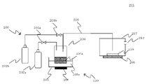
- FIG. 1 is a schematic configuration diagram showing an example of a film forming apparatus used in a film forming method according to the present invention
- FIG. 4 is a diagram showing the relationship between the TTV of the underlying substrate and the root-mean-square roughness of the surface of the crystalline oxide film according to the present invention
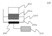
- It is a schematic block diagram which shows an example of the misting part used for this invention.
- the inventors of the present invention have found a laminated structure having a base substrate and a crystalline oxide film containing gallium oxide as a main component, wherein the surface of the crystalline oxide film is The root-mean-square roughness of the surface is 0.2 ⁇ m or less, the diameter of the base substrate is 50 mm (2 inches) or more, and the TTV of the base substrate is 30 ⁇ m or less. has a smooth crystalline oxide film, and when applied to a semiconductor device, it becomes a laminated structure with excellent semiconductor characteristics, and completed the present invention.
- the present inventors provide a method for manufacturing a laminated structure, a mist generation step of misting a gallium-containing raw material solution to generate a mist in the mist generating unit; a carrier gas supplying step of supplying a carrier gas for transporting the mist to the misting section; a conveying step of conveying the mist from the mist generating unit to the film forming chamber in which the base substrate is installed by the carrier gas via a supply pipe connecting the mist generating unit and the film forming chamber; a film formation step of heat-treating the conveyed mist to form a film on the underlying substrate;
- a method for manufacturing a laminated structure characterized in that a base substrate having a diameter of 50 mm or more and a TTV of 30 ⁇ m or less is used as the base substrate, and has a crystalline oxide film with a smooth surface, and when applied to a semiconductor device.
- the inventors have found that it is possible to manufacture a laminated structure having excellent semiconductor characteristics, and have completed the present
- the term "mist” as used in the present invention refers to a general term for fine particles of liquid dispersed in gas, and includes what is called fog, liquid droplets, and the like. Description will be made below with reference to the drawings.
- FIG. 1 shows a semiconductor device 100 having a laminated structure 110 of the present invention.
- a laminated structure 110 of the present invention has a base substrate 101 and a crystalline oxide film 103 containing gallium oxide as a main component.
- the root-mean-square roughness is 0.2 ⁇ m or less
- the diameter of the base substrate 101 is 50 mm (2 inches) or more
- the TTV of the base substrate 101 is 30 ⁇ m or less.
- the inventors of the present invention conducted extensive investigations, and found that the RMS of the surface of the crystalline oxide film sharply increased when the TTV of the underlying substrate exceeded 30 ⁇ m, as shown in FIG. As will be described later, the cause is considered to be deterioration of thermal contact with the heater and an increase in thermal resistance. Therefore, in the present invention, the TTV is set to 30 ⁇ m or less.
- the root mean square of the surface 103c of the crystalline oxide film 103 can be reduced.
- the square root roughness is 0.2 ⁇ m or less.
- the base substrate for the laminated structure of the present invention has a diameter of 50 mm (2 inches) or more and a TTV of 30 ⁇ m or less.
- the upper limit of the diameter is not particularly limited, it can be, for example, 300 mm or less.
- the lower limit of TTV is not particularly limited, but can be set to 0.1 ⁇ m or more, for example.
- TTV is an abbreviation for total thickness variation, and is the difference between the maximum value and the minimum value of the height measured in the thickness direction with the back surface of the wafer as the reference plane, over the entire surface of the wafer.
- the TTV of the base substrate is 30 ⁇ m or less.
- the TTV of the laminated structure obtained at this time is also 30 ⁇ m or less.
- TTV can be measured by a micrometer, a capacitance method, an optical interference method, a laser confocal method, or the like.
- the Ra of the surface opposite to the surface 103c having the crystalline oxide film of the laminated structure may be 0.5 ⁇ m or less.
- the waviness Wa of the surface opposite to the surface 103c having the crystalline oxide film of the laminated structure may be 50 ⁇ m or less.
- the waviness Wa is defined as "the amount of deviation of the planar shape from the geometrically correct plane".
- the waviness Wa may be measured on one or more arbitrary straight lines on the mounting surface that are appropriately determined according to the shape of the mounting surface. For example, when the placement surface is circular, the diameter of the circle on two straight lines perpendicular to each other at the center of the circle can be used as the measurement length.
- Waviness Wa is measured by a non-contact measurement method using a laser microscope or a confocal microscope, such as a stylus method, an atomic force microscope (AFM) method, or an optical interferometry method, a confocal method, or an image synthesizing method using focal point movement. Refers to the value obtained by calculating based on JIS B 0601 using the shape measurement results.
- the thickness of the base substrate is preferably 100-5000 ⁇ m. Within this range, good handling is achieved, thermal resistance is reduced during film formation, and a good quality film can be obtained.
- the base substrate is not particularly limited as long as it serves as a support for the crystalline oxide film.
- the material is not particularly limited, and a known substrate can be used, and it may be an organic compound or an inorganic compound.
- a known substrate can be used, and it may be an organic compound or an inorganic compound.
- polysulfone, polyethersulfone, polyphenylene sulfide, polyetheretherketone, polyimide, polyetherimide, fluororesin, metals such as iron, aluminum, stainless steel, and gold, quartz, glass, calcium carbonate, gallium oxide, ZnO, etc. is mentioned.
- single crystal substrates such as silicon, sapphire, ⁇ -type gallium oxide, lithium tantalate, lithium niobate, SiC, GaN, iron oxide, and chromium oxide can be used.
- a single crystal substrate as described above is desirable for the underlying substrate of the laminated structure of the present invention. With these, a crystalline oxide film of better quality can be obtained.
- sapphire substrates, lithium tantalate substrates, and lithium niobate substrates are relatively inexpensive and industrially advantageous.
- the RMS of the underlying substrate surface is preferably 0.1 ⁇ m or less. By using such a substrate, it becomes easier to obtain a crystalline oxide film having an RMS of 0.2 ⁇ m or less.
- the density of particles of 0.5 ⁇ m or more on the base substrate is preferably 50/cm 2 or less, and the metal impurity density is preferably 1 ⁇ 10 11 /cm 2 or less. By using such a base substrate, it becomes easier to obtain a crystalline oxide film with good crystallinity.
- the crystalline oxide film according to the laminated structure of the present invention is a crystalline oxide film containing gallium oxide as a main component, and the root mean square of the surface of the crystalline oxide film containing gallium oxide as a main component is Roughness is 0.2 ⁇ m or less.
- the lower limit of the root-mean-square roughness is not particularly limited, it can be, for example, 0.0001 ⁇ m or more.
- a crystalline oxide film is generally composed of metal and oxygen, but in the crystalline oxide film according to the laminated structure of the present invention, gallium may be used as the main component of the metal.
- gallium in the present invention, "mainly containing gallium” means that 50 to 100% of the metal component is gallium.
- Metal components other than gallium may include, for example, one or more metals selected from iron, indium, aluminum, vanadium, titanium, chromium, rhodium, iridium, nickel and cobalt.
- a dopant element may be contained in the crystalline oxide film.
- Examples include n-type dopants such as tin, germanium, silicon, titanium, zirconium, vanadium, or niobium, or p-type dopants such as copper, silver, nickel, tin, iridium, rhodium, cobalt, and magnesium, but are not particularly limited.
- the dopant concentration may be, for example, about 1 ⁇ 10 16 /cm 3 to 1 ⁇ 10 22 /cm 3 , and a low concentration of about 1 ⁇ 10 17 /cm 3 or less may be about 1 ⁇ 10 20 /cm 3 .
- the concentration may be as high as cm 3 or more.
- the crystal structure of the crystalline oxide film is not particularly limited, and may be a ⁇ -gallia structure, a corundum structure, or a cubic crystal. Although a plurality of crystal structures may be mixed or may be polycrystalline, it is preferably a single crystal or uniaxially oriented film. Whether it is a single crystal or uniaxially oriented film can be confirmed by an X-ray diffraction device, an electron beam diffraction device, or the like. When the film is irradiated with X-rays or electron beams, a diffraction image corresponding to the crystal structure is obtained, but only specific peaks appear when the film is uniaxially oriented. From this, it can be determined that the film is uniaxially oriented.
- the root mean square roughness (RMS) is not particularly limited as long as it is 0.2 ⁇ m or less.
- the root-mean-square roughness (RMS) is calculated based on JIS B 0601 (corresponding to Rq in the same standard) using surface shape measurement results for a 10 ⁇ m square region with an atomic force microscope (AFM). Say the value obtained.
- Arithmetic mean roughness (Ra) is a value calculated according to JIS B 0601 using the results of surface shape measurement of a 10 ⁇ m square region with an atomic force microscope (AFM).
- the film thickness of the crystalline oxide film is not particularly limited, it is preferably 1 ⁇ m or more.
- the upper limit is not particularly limited. For example, it may be 100 ⁇ m or less, preferably 50 ⁇ m or less, more preferably 20 ⁇ m or less. With such a film thickness, when applied to a semiconductor device, the semiconductor characteristics such as improved withstand voltage can be obtained.
- the separate layer is a layer having a composition different from that of the underlying substrate and the outermost crystalline oxide film, and is also called a buffer layer.
- the buffer layer may be an oxide semiconductor film, an insulating film, a metal film, or the like, and examples of materials include Al 2 O 3 , Ga 2 O 3 , Cr 2 O 3 , Fe 2 O 3 , and In 2 O. 3 , Rh 2 O 3 , V 2 O 3 , Ti 2 O 3 , Ir 2 O 3 and the like are preferably used.
- the thickness of the buffer layer is preferably 0.1 ⁇ m to 2 ⁇ m.
- FIG. 2 shows an example of a film forming apparatus 201 according to the method for manufacturing a laminated structure of the present invention.
- the film formation apparatus 201 includes a mist formation section 220 that forms a mist from a raw material solution 204a containing gallium to generate mist, a carrier gas supply section 230 that supplies a carrier gas for conveying the mist, a mist formation section 220, and a film formation chamber.
- the raw material solution 204a containing gallium is misted to generate mist.
- the misting means is not particularly limited as long as it can mist the raw material solution 204a containing gallium, and may be a known misting means, but it is preferable to use a misting means using ultrasonic vibration. This is because mist can be made more stably.
- the mist generation unit 220 includes a mist generation source 204 containing a gallium-containing raw material solution 204a, a container 205 containing a medium capable of transmitting ultrasonic vibrations, such as water 205a, and an ultrasonic transducer attached to the bottom surface of the container 205.
- a sonic transducer 206 may be included.
- mist generation source 204 which is a container containing raw material solution 204a containing gallium, can be housed in container 205 containing water 205a using a support (not shown). can.
- An ultrasonic transducer 206 may be provided at the bottom of the container 205, and the ultrasonic transducer 206 and the oscillator 216 may be connected. When the oscillator 216 is operated, the ultrasonic vibrator 206 vibrates, ultrasonic waves propagate through the water 205a into the mist generation source 204, and the raw material solution 204a containing gallium becomes mist. can be done.
- the raw material solution 204a containing gallium can be misted, and the material contained in the solution is not particularly limited as long as it contains gallium, and may be an inorganic material or an organic material.
- Metals or metal compounds are preferably used, for example, those containing one or more metals selected from gallium, iron, indium, aluminum, vanadium, titanium, chromium, rhodium, nickel and cobalt may be used. I don't mind.
- a solution obtained by dissolving or dispersing a metal in the form of a complex or a salt in an organic solvent or water can be suitably used.
- Salt forms include, for example, halide salts such as metal chloride salts, metal bromide salts, and metal iodide salts. Further, a solution obtained by dissolving the above metal in a hydrogen halide such as hydrobromic acid, hydrochloric acid or hydroiodic acid can also be used as a salt solution. Examples of forms of the complex include acetylacetonate complexes, carbonyl complexes, ammine complexes, hydride complexes, and the like. Acetylacetonate complexes can also be formed by mixing acetylacetone with the aforementioned salt solutions.
- the metal concentration in the raw material solution 204a containing gallium is not particularly limited, and can be 0.005 to 1 mol/L.
- the raw material solution 204a containing gallium may be mixed with additives such as hydrohalic acid and oxidizing agents.
- the hydrohalic acid includes, for example, hydrobromic acid, hydrochloric acid, hydroiodic acid, etc. Among them, hydrobromic acid and hydroiodic acid are preferable.
- the oxidizing agent include hydrogen peroxide (H 2 O 2 ), sodium peroxide (Na 2 O 2 ), barium peroxide (BaO 2 ), benzoyl peroxide (C 6 H 5 CO) 2 O 2 and the like.
- the raw material solution 204a containing gallium may contain a dopant.
- a dopant is not specifically limited. Examples include n-type dopants such as tin, germanium, silicon, titanium, zirconium, vanadium or niobium, or p-type dopants such as copper, silver, iridium, rhodium and magnesium.
- the carrier gas supply section 230 has a carrier gas source 202a for supplying carrier gas.
- a flow control valve 203a for adjusting the flow rate of the carrier gas sent from the carrier gas source 202a may be provided.
- a carrier gas source 202b for dilution that supplies a carrier gas for dilution and a flow control valve 203b for adjusting the flow rate of the carrier gas for dilution sent out from the carrier gas source 202b for dilution can also be provided as necessary. .
- the type of carrier gas is not particularly limited, and can be appropriately selected according to the film to be deposited. Examples thereof include oxygen, ozone, inert gases such as nitrogen and argon, and reducing gases such as hydrogen gas and forming gas. Also, the number of carrier gases may be one, or two or more. For example, as the second carrier gas, a diluent gas obtained by diluting the same gas as the first carrier gas with another gas (for example, diluted 10 times) may be used, or air may be used.
- the flow rate of carrier gas is not particularly limited. For example, when forming a film on a base substrate of 50 mm (2 inches), the flow rate of the carrier gas is preferably 0.05 to 50 L/min, more preferably 5 to 20 L/min.
- the film forming apparatus 201 has a supply pipe 209 that connects the misting section 220 and the film forming chamber 207 .
- the mist is carried by the carrier gas from the mist generation source 204 of the misting section 220 through the supply pipe 209 and supplied into the film forming chamber 207 .
- a quartz tube, a glass tube, a resin tube, or the like can be used for the supply tube 209, for example.
- a base substrate 210 is installed in the deposition chamber 207, and a heater 208 for heating the base substrate 210 can be provided.
- the heater 208 may be provided outside the film formation chamber 207 as shown in FIG. 2, or may be provided inside the film formation chamber 207 .
- the deposition chamber 207 may be provided with an exhaust port 212 for exhaust gas at a position that does not affect the supply of mist to the base substrate 210 .
- the base substrate 210 may be placed on the upper surface of the film formation chamber 207 to face down, or the base substrate 210 may be placed on the bottom surface of the film formation chamber 207 to face up.
- a stage for placing the underlying substrate 210 may be installed in the film formation chamber 207 .
- the surface roughness Ra of the stage may be 0.5 ⁇ m or less.
- the surface roughness Ra is 0.5 ⁇ m or less, the contact area with the base substrate 210 does not decrease, so the heat conduction does not deteriorate, and the temperature of the substrate surface during film formation does not decrease due to the film-forming raw material mist.
- the crystal orientation of the film does not deteriorate.
- the waviness Wa may be 50 ⁇ m or less. The smaller the waviness Wa, the better, and although the lower limit is not particularly limited, it can be, for example, 0.5 ⁇ m or more.
- Wa is 50 ⁇ m or less, the contact area with the underlying substrate 210 increases, thereby improving heat conduction, preventing a significant decrease in the temperature of the substrate surface during film formation due to the film-forming raw material mist, and crystal orientation of the semiconductor film. does not reduce sexuality.
- the present invention is characterized in that the diameter of the substrate is set to 50 mm or more and the TTV is set to 30 ⁇ m or less in the mist CVD.
- the mist CVD method requires the raw material to reach the substrate surface in a liquid state. Therefore, the temperature of the substrate surface is greatly lowered. At this time, if the TTV of the substrate is larger than 30 ⁇ m, thermal contact between the substrate and the heater deteriorates. At the same time, the portion where the substrate thickness is thick has a relatively large thermal resistance. Due to these influences, the decrease in the substrate surface temperature is further increased. This is particularly noticeable when the diameter is 50 mm or more. If the film is formed in this state, abnormal growth occurs on the film surface, and the surface roughness of the obtained film becomes extremely large exceeding 0.2 ⁇ m.
- the root mean square roughness of the film surface in the as-grown state is 0.0.
- a laminated structure of 2 ⁇ m or less can be obtained.
- the raw material solution 204a containing gallium mixed by the method described above is placed in the mist generation source 204, the underlying substrate 210 is placed in the film forming chamber 207, and the heater 208 is activated.
- the flow control valves 203a and 203b are opened to supply the carrier gas from the carrier gas sources 202a and 202b into the film forming chamber 207.
- the carrier gas is supplied. Adjust the flow rate and the flow rate of the carrier gas for dilution.
- the ultrasonic oscillator 206 is vibrated, and the vibration is propagated through the water 205a to the gallium-containing raw material solution 204a, thereby misting the gallium-containing raw material solution 204a to generate mist. .
- a carrier gas for transporting mist is supplied to the misting section 220 .
- the mist is transported from the mist generating unit 220 to the film forming chamber 207 via the supply pipe 209 that connects the mist generating unit 220 and the film forming chamber 207 using a carrier gas.
- the mist transported to the film forming chamber 207 is heated to cause a thermal reaction, thereby forming a film on part or all of the surface of the underlying substrate 210 .
- the mist reacts by heating it is sufficient that the mist reacts by heating, and the reaction conditions are not particularly limited. It can be appropriately set according to the raw material and the film-formed material.
- the heating temperature can be in the range of 120-600°C, preferably in the range of 200-600°C, more preferably in the range of 300-550°C.
- the thermal reaction may be carried out under vacuum, under a non-oxygen atmosphere, under a reducing gas atmosphere, under an air atmosphere, or under an oxygen atmosphere, and may be appropriately set according to the film to be deposited.
- the reaction pressure may be under atmospheric pressure, under increased pressure or under reduced pressure, but film formation under atmospheric pressure is preferable because the apparatus configuration can be simplified.
- a buffer layer may be appropriately provided between the base substrate and the film.
- the method for forming the buffer layer is not particularly limited, and it can be formed by a known method such as a sputtering method or a vapor deposition method. It is simple and easy to form. Specifically, one or more metals selected from aluminum, gallium, chromium, iron, indium, rhodium, vanadium, titanium, and iridium are dissolved or dispersed in water in the form of complexes or salts. can be suitably used as the raw material aqueous solution.
- Examples of forms of the complex include acetylacetonate complexes, carbonyl complexes, ammine complexes, hydride complexes, and the like.
- Salt forms include, for example, metal chloride salts, metal bromide salts, and metal iodide salts.
- a solution obtained by dissolving the above metal in hydrobromic acid, hydrochloric acid, hydroiodic acid, or the like can also be used as an aqueous salt solution.
- the solute concentration is preferably 0.005 to 1 mol/L, and the dissolution temperature is 20° C. or higher.
- the buffer layer can also be formed under the same conditions as above. After forming a buffer layer with a predetermined thickness, a crystalline oxide film is formed.
- the film obtained by the film formation method according to the method for manufacturing the laminated structure of the present invention may be heat-treated at 200 to 600.degree. As a result, unreacted species and the like in the film are removed, and a higher quality laminated structure can be obtained.
- the heat treatment may be performed in air, in an oxygen atmosphere, or in an inert gas atmosphere such as nitrogen or argon.
- the heat treatment time is appropriately determined, and can be, for example, 5 to 240 minutes.
- the crystalline oxide film may be separated from the base substrate.
- the peeling means is not particularly limited, and known means may be used. Examples of peeling means include means for applying mechanical impact to peel, means for applying heat and utilizing thermal stress for peeling, means for peeling by applying vibration such as ultrasonic waves, and means for peeling by etching. etc. By the peeling, the crystalline oxide film can be obtained as a self-supporting film.
- FIG. 1 shows a preferred example of a semiconductor device 100 using the laminated structure of the present invention.
- a crystalline oxide film 103 is formed on an underlying substrate 101 .
- the crystalline oxide film 103 is formed by stacking an insulating thin film 103a and a conductive thin film 103b in order from the base substrate 101 side.
- a gate insulating film 105 is formed on the conductive thin film 103b.
- a gate electrode 107 is formed on the gate insulating film 105 .
- Source/drain electrodes 109 are formed on the conductive thin film 103b so as to sandwich the gate electrode 107 therebetween. According to such a configuration, the depletion layer formed in the conductive thin film 103b can be controlled by the gate voltage applied to the gate electrode 107, enabling transistor operation (FET device).
- FET device transistor operation
- Semiconductor devices formed using the laminated structure of the present invention include transistors such as MIS, HEMT, IGBT and TFT, Schottky barrier diodes utilizing semiconductor-metal junction, PN or PIN diodes and light emitting/receiving elements are included.
- the laminated structure of the present invention is useful for improving the characteristics of these devices.
- the present invention is characterized in that the diameter of the substrate is set to 50 mm or more and the TTV is set to 30 ⁇ m or less in the mist CVD.
- the mist CVD method requires the raw material to reach the substrate surface in a liquid state. Therefore, the temperature of the substrate surface is greatly lowered. At this time, if the TTV of the substrate is larger than 30 ⁇ m, thermal contact between the substrate and the heater deteriorates. At the same time, the portion where the substrate thickness is thick has a relatively large thermal resistance. Due to these influences, the decrease in the substrate surface temperature is further increased. This is particularly noticeable when the diameter is 50 mm or more. If the film is formed in this state, abnormal growth occurs on the film surface, and the surface roughness of the obtained film becomes extremely large exceeding 0.2 ⁇ m.
- the root mean square roughness of the film surface in the as-grown state is 0.0.
- a laminated structure of 2 ⁇ m or less can be obtained.
- the raw material solution 204a containing gallium mixed by the method described above is placed in the mist generation source 204, the underlying substrate 210 is placed in the film forming chamber 207, and the heater 208 is activated.
- the flow control valves 203a and 203b are opened to supply the carrier gas from the carrier gas sources 202a and 202b into the film forming chamber 207.
- the carrier gas is supplied. Adjust the flow rate and the flow rate of the carrier gas for dilution.
- the ultrasonic oscillator 206 is vibrated, and the vibration is propagated through the water 205a to the raw material solution 204a containing gallium, thereby misting the raw material solution 204a containing gallium to generate mist. .
- a carrier gas for transporting mist is supplied to the misting section 220 .
- the mist is transported from the mist generating unit 220 to the film forming chamber 207 via the supply pipe 209 that connects the mist generating unit 220 and the film forming chamber 207 with a carrier gas.
- the mist transported to the film forming chamber 207 is heated to cause a thermal reaction, thereby forming a film on part or all of the surface of the underlying substrate 210 .
- the mist reacts by heating it is sufficient that the mist reacts by heating, and the reaction conditions are not particularly limited. It can be appropriately set according to the raw material and the film-formed material.
- the heating temperature can be in the range of 120-600°C, preferably in the range of 200-600°C, more preferably in the range of 300-550°C.
- the thermal reaction may be carried out under vacuum, under a non-oxygen atmosphere, under a reducing gas atmosphere, under an air atmosphere, or under an oxygen atmosphere, and may be appropriately set according to the film to be deposited.
- the reaction pressure may be under atmospheric pressure, under increased pressure or under reduced pressure, but film formation under atmospheric pressure is preferable because the apparatus configuration can be simplified.
- a buffer layer may be appropriately provided between the base substrate and the film.
- the method for forming the buffer layer is not particularly limited, and it can be formed by a known method such as a sputtering method or a vapor deposition method. It is simple and easy to form. Specifically, one or more metals selected from aluminum, gallium, chromium, iron, indium, rhodium, vanadium, titanium, and iridium are dissolved or dispersed in water in the form of complexes or salts. can be suitably used as the raw material aqueous solution.
- Examples of forms of the complex include acetylacetonate complexes, carbonyl complexes, ammine complexes, hydride complexes, and the like.
- Salt forms include, for example, metal chloride salts, metal bromide salts, and metal iodide salts.
- a solution obtained by dissolving the above metal in hydrobromic acid, hydrochloric acid, hydroiodic acid, or the like can also be used as an aqueous salt solution.
- the solute concentration is preferably 0.005 to 1 mol/L, and the dissolution temperature is 20° C. or higher.
- the buffer layer can also be formed under the same conditions as above. After forming a buffer layer with a predetermined thickness, a crystalline oxide film is formed.
- the film obtained by the film forming system according to the manufacturing system of the laminated structure of the present invention may be heat-treated at 200 to 600.degree. As a result, unreacted species and the like in the film are removed, and a higher quality laminated structure can be obtained.
- the heat treatment may be performed in air, in an oxygen atmosphere, or in an inert gas atmosphere such as nitrogen or argon.
- the heat treatment time is appropriately determined, and can be, for example, 5 to 240 minutes.
- the crystalline oxide film may be separated from the base substrate.
- the peeling means is not particularly limited, and known means may be used. Examples of peeling means include means for applying mechanical impact to peel, means for applying heat and utilizing thermal stress for peeling, means for peeling by applying vibration such as ultrasonic waves, and means for peeling by etching. etc. By the peeling, the crystalline oxide film can be obtained as a self-supporting film.
- the laminated structure manufacturing system confirms that the TTV is 30 ⁇ m or less when the diameter of the base substrate is 50 mm or more, prior to placing the base substrate in the film formation chamber. is preferred.
- the film forming apparatus 201 includes a carrier gas source 202a that supplies a carrier gas, a flow control valve 203a that adjusts the flow rate of the carrier gas sent from the carrier gas source 202a, and a dilution carrier gas that supplies a dilution carrier gas.
- source 202b a flow control valve 203b for adjusting the flow rate of the carrier gas for dilution sent from the carrier gas source 202b for dilution, a mist generation source 204 containing a raw material solution 204a containing gallium, and water 205a.
- a container 205 an ultrasonic transducer 206 attached to the bottom surface of the container 205, a film formation chamber 207 having a heater 208, and a supply pipe 209 made of quartz connecting the mist generation source 204 to the film formation chamber 207. and have.
- a c-plane sapphire substrate with a diameter of 100 mm (4 inches) was prepared as the base substrate 210 .
- TTV was measured by a light interference type flatness tester, it was 16 ⁇ m.
- the substrate was placed in the film formation chamber 207, and the heater 208 was operated to raise the temperature to 500.degree.
- raw material solution containing gallium a raw material solution containing gallium was prepared.
- the solvent was ultrapure water and the solute was gallium bromide.
- the gallium concentration was set to 0.1 mol/L, and this was used as the raw material solution 204a containing gallium.
- the raw material solution 204 a containing gallium obtained as described above was placed in the mist generation source 204 . Subsequently, the flow control valves 203a and 203b are opened to supply the carrier gas from the carrier gas sources 202a and 202b into the film forming chamber 207. After sufficiently replacing the atmosphere in the film forming chamber 207 with the carrier gas, the carrier gas is supplied. The flow rate was adjusted to 2 L/min, and the flow rate of the carrier gas for dilution was adjusted to 6 L/min. Nitrogen was used as the carrier gas.
- the ultrasonic oscillator 206 was vibrated at 2.4 MHz, and the vibration was propagated through the water 205a to the gallium-containing raw material solution 204a, thereby misting the gallium-containing raw material solution 204a to generate mist.
- This mist was introduced into the film formation chamber 207 through the supply pipe 209 by the carrier gas.
- a thin film of gallium oxide was formed on the base substrate 210 by thermally reacting the mist in the film forming chamber 207 under the conditions of 500° C. under atmospheric pressure.
- the film formation time was 30 minutes.
- Example 2 and 3 A c-plane sapphire substrate having a diameter of 100 mm (4 inches) with different TTVs was prepared as the base substrate 210 . Specifically, substrates with a TTV of 3 and 26 ⁇ m were prepared, and film formation and evaluation were performed under the same conditions as in Example 1 except for this. As a result, the RMS was 2 and 8 nm, respectively. Also, the film thicknesses were 0.49 and 0.51 ⁇ m, respectively.
- Example 4 Film formation and evaluation were performed under the same conditions as in Example 1, except that the film formation time was 60 minutes. As a result, the film thickness was 1.1 ⁇ m and the RMS was 11 nm.
- Example 5 Film formation and evaluation were performed under the same conditions as in Example 1, except that the film formation time was 480 minutes. As a result, the film thickness was 8.5 ⁇ m and the RMS was 15 nm.
- Example 6 Film formation and evaluation were performed under the same conditions as in Example 1, except that the Ra of the non-film-forming surface of the substrate was set to 0.41 ⁇ m. As a result, RMS was 7 nm. Moreover, the film thickness was 0.51 ⁇ m.
- Example 7 Film formation and evaluation were carried out under the same conditions as in Example 1, except that Wa on the non-film-forming surface of the substrate was 47.7 ⁇ m. As a result, RMS was 10 nm. Moreover, the film thickness was 0.53 ⁇ m.
- Example 8 Film formation and evaluation were performed under the same conditions as in Example 1, except that a copper plate (stage) was placed on the heater and Ra of the copper plate was set to 0.45 ⁇ m. As a result, RMS was 5 nm. Moreover, the film thickness was 0.48 ⁇ m.
- Example 9 Film formation and evaluation were performed under the same conditions as in Example 1, except that a copper plate (stage) was placed on the heater and Wa of the copper plate was set to 48.2 ⁇ m. As a result, the RMS was 6 nm. Moreover, the film thickness was 0.50 ⁇ m.
- FIG. 1 A graph summarizing Examples 1, 2 and 3 and Comparative Examples 1 and 2 is shown in FIG. It can be seen that when the TTV of the underlying substrate exceeds 30 ⁇ m, the RMS of the surface of the crystalline oxide film increases sharply. As mentioned above, the deterioration of thermal contact with the heater and the increase in thermal resistance are thought to be the causes.
- the present invention is not limited to the above embodiments.
- the above-described embodiment is an example, and any device having substantially the same configuration as the technical idea described in the claims of the present invention and exhibiting the same effect is the present invention. included in the technical scope of
Landscapes
- Engineering & Computer Science (AREA)
- Chemical & Material Sciences (AREA)
- Physics & Mathematics (AREA)
- Power Engineering (AREA)
- Microelectronics & Electronic Packaging (AREA)
- Computer Hardware Design (AREA)
- Manufacturing & Machinery (AREA)
- General Physics & Mathematics (AREA)
- Condensed Matter Physics & Semiconductors (AREA)
- Materials Engineering (AREA)
- Crystallography & Structural Chemistry (AREA)
- Organic Chemistry (AREA)
- Metallurgy (AREA)
- General Chemical & Material Sciences (AREA)
- Chemical Kinetics & Catalysis (AREA)
- Inorganic Chemistry (AREA)
- Mechanical Engineering (AREA)
- Dispersion Chemistry (AREA)
- Crystals, And After-Treatments Of Crystals (AREA)
- Laminated Bodies (AREA)
- Recrystallisation Techniques (AREA)
- Control Of Motors That Do Not Use Commutators (AREA)
- Metal-Oxide And Bipolar Metal-Oxide Semiconductor Integrated Circuits (AREA)
- Internal Circuitry In Semiconductor Integrated Circuit Devices (AREA)
Priority Applications (4)
| Application Number | Priority Date | Filing Date | Title |
|---|---|---|---|
| EP22795493.0A EP4332279A1 (en) | 2021-04-28 | 2022-03-30 | Multilayer structure, semiconductor device and method for producing multilayer structure |
| KR1020237036427A KR20240000497A (ko) | 2021-04-28 | 2022-03-30 | 적층구조체, 반도체장치 및 적층구조체의 제조방법 |
| JP2023517200A JPWO2022230577A1 (zh) | 2021-04-28 | 2022-03-30 | |
| CN202280030633.XA CN117321256A (zh) | 2021-04-28 | 2022-03-30 | 层叠结构体、半导体装置以及层叠结构体的制造方法 |
Applications Claiming Priority (2)
| Application Number | Priority Date | Filing Date | Title |
|---|---|---|---|
| JP2021-076657 | 2021-04-28 | ||
| JP2021076657 | 2021-04-28 |
Publications (1)
| Publication Number | Publication Date |
|---|---|
| WO2022230577A1 true WO2022230577A1 (ja) | 2022-11-03 |
Family
ID=83847408
Family Applications (1)
| Application Number | Title | Priority Date | Filing Date |
|---|---|---|---|
| PCT/JP2022/015911 WO2022230577A1 (ja) | 2021-04-28 | 2022-03-30 | 積層構造体、半導体装置及び積層構造体の製造方法 |
Country Status (6)
| Country | Link |
|---|---|
| EP (1) | EP4332279A1 (zh) |
| JP (1) | JPWO2022230577A1 (zh) |
| KR (1) | KR20240000497A (zh) |
| CN (1) | CN117321256A (zh) |
| TW (2) | TWM633282U (zh) |
| WO (1) | WO2022230577A1 (zh) |
Citations (4)
| Publication number | Priority date | Publication date | Assignee | Title |
|---|---|---|---|---|
| JP2013028480A (ja) | 2011-07-27 | 2013-02-07 | Kochi Univ Of Technology | ドーパントを添加した結晶性の高い導電性α型酸化ガリウム薄膜およびその生成方法 |
| JP2015039033A (ja) * | 2006-12-28 | 2015-02-26 | サン−ゴバン セラミックス アンド プラスティクス,インコーポレイティド | サファイア基板 |
| JP2015199649A (ja) | 2014-03-31 | 2015-11-12 | 株式会社Flosfia | 結晶性積層構造体、半導体装置 |
| JP2021024184A (ja) * | 2019-08-02 | 2021-02-22 | 信越化学工業株式会社 | 積層体、半導体膜、半導体装置、半導体システム及び積層体の製造方法 |
-
2022
- 2022-03-22 TW TW111202820U patent/TWM633282U/zh unknown
- 2022-03-22 TW TW111110480A patent/TW202242209A/zh unknown
- 2022-03-30 KR KR1020237036427A patent/KR20240000497A/ko unknown
- 2022-03-30 WO PCT/JP2022/015911 patent/WO2022230577A1/ja active Application Filing
- 2022-03-30 EP EP22795493.0A patent/EP4332279A1/en active Pending
- 2022-03-30 JP JP2023517200A patent/JPWO2022230577A1/ja active Pending
- 2022-03-30 CN CN202280030633.XA patent/CN117321256A/zh active Pending
Patent Citations (4)
| Publication number | Priority date | Publication date | Assignee | Title |
|---|---|---|---|---|
| JP2015039033A (ja) * | 2006-12-28 | 2015-02-26 | サン−ゴバン セラミックス アンド プラスティクス,インコーポレイティド | サファイア基板 |
| JP2013028480A (ja) | 2011-07-27 | 2013-02-07 | Kochi Univ Of Technology | ドーパントを添加した結晶性の高い導電性α型酸化ガリウム薄膜およびその生成方法 |
| JP2015199649A (ja) | 2014-03-31 | 2015-11-12 | 株式会社Flosfia | 結晶性積層構造体、半導体装置 |
| JP2021024184A (ja) * | 2019-08-02 | 2021-02-22 | 信越化学工業株式会社 | 積層体、半導体膜、半導体装置、半導体システム及び積層体の製造方法 |
Non-Patent Citations (1)
| Title |
|---|
| "Electrical Conductive Corundum-Structured a-Ga O Thin Films on Sapphire with Tin-Doping Grown by Spray-Assisted Mist Chemical Vapor Deposition", JAPANESE JOURNAL OF APPLIED PHYSICS, vol. 51, 2012, pages 070203 |
Also Published As
| Publication number | Publication date |
|---|---|
| EP4332279A1 (en) | 2024-03-06 |
| TWM633282U (zh) | 2022-10-21 |
| TW202242209A (zh) | 2022-11-01 |
| KR20240000497A (ko) | 2024-01-02 |
| JPWO2022230577A1 (zh) | 2022-11-03 |
| CN117321256A (zh) | 2023-12-29 |
Similar Documents
| Publication | Publication Date | Title |
|---|---|---|
| JP7223515B2 (ja) | 成膜装置及び成膜方法 | |
| JP2024023981A (ja) | 結晶性酸化物薄膜、積層体及び結晶性酸化物薄膜の製造方法 | |
| WO2022230577A1 (ja) | 積層構造体、半導体装置及び積層構造体の製造方法 | |
| WO2022215621A1 (ja) | 積層体の製造方法、積層体の製造装置、積層体及び半導体装置 | |
| WO2023047895A1 (ja) | 成膜方法、成膜装置及び結晶性酸化物膜 | |
| WO2023149180A1 (ja) | 結晶性酸化物膜、積層構造体、半導体装置、及び結晶性酸化物膜の製造方法 | |
| WO2023053817A1 (ja) | 積層構造体、半導体装置及び結晶性酸化物膜の成膜方法 | |
| JP7313530B2 (ja) | 成膜方法 | |
| WO2024043049A1 (ja) | 成膜方法、成膜装置、及びα-Ga2O3膜 | |
| WO2023238587A1 (ja) | 成膜方法、及び成膜装置 | |
| JP7348777B2 (ja) | 積層構造体の製造方法及び半導体装置の製造方法 | |
| JP7078581B2 (ja) | 積層構造体及び半導体装置並びに積層構造体の製造方法 | |
| JP7161457B2 (ja) | 積層構造体及び半導体装置並びに積層構造体の製造方法 | |
| JP7436333B2 (ja) | 成膜方法及び成膜装置 | |
| WO2023021815A1 (ja) | 半導体膜及び複合基板 | |
| JP7492621B2 (ja) | 成膜装置 | |
| JP2023156732A (ja) | 結晶性積層構造体、半導体装置及び結晶性積層構造体の製造方法 | |
| JP7097861B2 (ja) | 積層構造体、半導体装置及び半導体システム | |
| JP2021038112A (ja) | 積層構造体、半導体装置及び半導体システム | |
| TW202235664A (zh) | 氧化物半導體膜及其成膜方法、半導體裝置 | |
| JP2021031375A (ja) | 積層構造体、半導体装置及び結晶性酸化膜の成膜方法 | |
| CN114302982A (zh) | 层叠结构体及层叠结构体的制造方法 | |
| JP2021038116A (ja) | 積層構造体及び半導体装置並びに積層構造体の製造方法 |
Legal Events
| Date | Code | Title | Description |
|---|---|---|---|
| 121 | Ep: the epo has been informed by wipo that ep was designated in this application |
Ref document number: 22795493 Country of ref document: EP Kind code of ref document: A1 |
|
| WWE | Wipo information: entry into national phase |
Ref document number: 2023517200 Country of ref document: JP |
|
| WWE | Wipo information: entry into national phase |
Ref document number: 202280030633.X Country of ref document: CN |
|
| WWE | Wipo information: entry into national phase |
Ref document number: 2022795493 Country of ref document: EP |
|
| NENP | Non-entry into the national phase |
Ref country code: DE |
|
| ENP | Entry into the national phase |
Ref document number: 2022795493 Country of ref document: EP Effective date: 20231128 |