WO2022219790A1 - 荷電粒子線装置 - Google Patents
荷電粒子線装置 Download PDFInfo
- Publication number
- WO2022219790A1 WO2022219790A1 PCT/JP2021/015638 JP2021015638W WO2022219790A1 WO 2022219790 A1 WO2022219790 A1 WO 2022219790A1 JP 2021015638 W JP2021015638 W JP 2021015638W WO 2022219790 A1 WO2022219790 A1 WO 2022219790A1
- Authority
- WO
- WIPO (PCT)
- Prior art keywords
- charged particle
- particle beam
- shield
- bushing
- beam device
- Prior art date
- Legal status (The legal status is an assumption and is not a legal conclusion. Google has not performed a legal analysis and makes no representation as to the accuracy of the status listed.)
- Ceased
Links
Images


Classifications
-
- H—ELECTRICITY
- H01—ELECTRIC ELEMENTS
- H01J—ELECTRIC DISCHARGE TUBES OR DISCHARGE LAMPS
- H01J37/00—Discharge tubes with provision for introducing objects or material to be exposed to the discharge, e.g. for the purpose of examination or processing thereof
- H01J37/02—Details
- H01J37/16—Vessels; Containers
-
- H—ELECTRICITY
- H01—ELECTRIC ELEMENTS
- H01J—ELECTRIC DISCHARGE TUBES OR DISCHARGE LAMPS
- H01J37/00—Discharge tubes with provision for introducing objects or material to be exposed to the discharge, e.g. for the purpose of examination or processing thereof
- H01J37/02—Details
- H01J37/04—Arrangements of electrodes and associated parts for generating or controlling the discharge, e.g. electron-optical arrangement or ion-optical arrangement
- H01J37/06—Electron sources; Electron guns
- H01J37/07—Eliminating deleterious effects due to thermal effects or electric or magnetic fields
-
- H—ELECTRICITY
- H01—ELECTRIC ELEMENTS
- H01J—ELECTRIC DISCHARGE TUBES OR DISCHARGE LAMPS
- H01J37/00—Discharge tubes with provision for introducing objects or material to be exposed to the discharge, e.g. for the purpose of examination or processing thereof
- H01J37/02—Details
- H01J37/04—Arrangements of electrodes and associated parts for generating or controlling the discharge, e.g. electron-optical arrangement or ion-optical arrangement
- H01J37/09—Diaphragms; Shields associated with electron or ion-optical arrangements; Compensation of disturbing fields
-
- H—ELECTRICITY
- H01—ELECTRIC ELEMENTS
- H01J—ELECTRIC DISCHARGE TUBES OR DISCHARGE LAMPS
- H01J37/00—Discharge tubes with provision for introducing objects or material to be exposed to the discharge, e.g. for the purpose of examination or processing thereof
- H01J37/02—Details
- H01J37/24—Circuit arrangements not adapted to a particular application of the tube and not otherwise provided for
- H01J37/241—High voltage power supply or regulation circuits
-
- H—ELECTRICITY
- H01—ELECTRIC ELEMENTS
- H01J—ELECTRIC DISCHARGE TUBES OR DISCHARGE LAMPS
- H01J37/00—Discharge tubes with provision for introducing objects or material to be exposed to the discharge, e.g. for the purpose of examination or processing thereof
- H01J37/26—Electron or ion microscopes; Electron or ion diffraction tubes
- H01J37/28—Electron or ion microscopes; Electron or ion diffraction tubes with scanning beams
-
- H—ELECTRICITY
- H01—ELECTRIC ELEMENTS
- H01J—ELECTRIC DISCHARGE TUBES OR DISCHARGE LAMPS
- H01J37/00—Discharge tubes with provision for introducing objects or material to be exposed to the discharge, e.g. for the purpose of examination or processing thereof
- H01J37/26—Electron or ion microscopes; Electron or ion diffraction tubes
- H01J37/295—Electron or ion diffraction tubes
- H01J37/2955—Electron or ion diffraction tubes using scanning ray
-
- H—ELECTRICITY
- H01—ELECTRIC ELEMENTS
- H01J—ELECTRIC DISCHARGE TUBES OR DISCHARGE LAMPS
- H01J2237/00—Discharge tubes exposing object to beam, e.g. for analysis treatment, etching, imaging
- H01J2237/04—Means for controlling the discharge
- H01J2237/047—Changing particle velocity
- H01J2237/0473—Changing particle velocity accelerating
Definitions
- the present invention relates to a charged particle beam device, and more particularly to a charged particle beam device having a highly reliable charged particle beam generator.
- electron beam generators for electron microscopes are largely divided into those that irradiate the specimen with an electron beam generated from an electron gun, and those that irradiate the specimen with an electron beam generated from the electron gun that is further accelerated by an accelerating tube. can be separated.
- the former is mainly applied to scanning electron microscopes that do not require large electron energy, and the latter is mainly applied to transmission electron microscopes that require large electron energy. Since a transmission electron microscope uses a high voltage of 100 kV or higher, a highly reliable insulating structure that does not cause dielectric breakdown is required.
- An electron gun described in Patent Document 1 is an example of an electron beam generator using an accelerating tube.
- cooling of the electron gun is achieved by circulating insulating gas in a highly reliable insulating structure having a shield in an insulating gas space.
- the electron gun has projections, and since the tip of the projection is in a high electric field, there is a possibility that dielectric breakdown may occur due to discharge.
- the electric field at the tip of the projection can be relaxed, and dielectric breakdown due to discharge can be suppressed.
- Each electrode or acceleration electrode of the electron gun must be set to a different potential.
- a multi-core bushing called a cable head introduces a current from the air into the insulating gas, A voltage is applied to each by .
- the present invention provides a charged particle beam device capable of realizing a highly reliable insulating structure.
- a charged particle beam apparatus irradiates a sample with a charged particle beam from a charged particle beam generator, detects the charged particles generated from the sample, and generates a sample image or processes the sample.
- the charged particle beam generator comprises a charged particle source and a shield arranged inside a metal housing filled with an insulating gas, and an accelerator arranged below the charged particle source. and an electrode, and power is supplied to the acceleration electrode through the shield.
- a charged particle beam apparatus according to the present invention irradiates a sample with a charged particle beam from a charged particle beam generator, detects charged particles generated from the sample, and generates a sample image or processes the sample.
- the charged particle beam generator comprises a charged particle source and a shield arranged inside a metal housing filled with an insulating gas, and an accelerating electrode arranged below the charged particle source.
- a potential of the shield is set to be the same as that of any part of the charged particle source, and power is supplied to the acceleration electrode by wiring for power supply to the accelerating tube arranged inside the shield.
- FIG. 1 is a longitudinal sectional view of an electron beam generator of Example 1 according to one embodiment of the present invention
- FIG. 1 is an overall configuration diagram of a charged particle beam device according to an embodiment of the present invention
- FIG. 5 is a vertical cross-sectional view of an electron beam generator of Example 2 according to another example of the present invention
- FIG. 10 is a vertical cross-sectional view of an electron beam generator of Example 3 according to another example of the present invention
- FIG. 10 is a vertical cross-sectional view of an electron beam generator of Example 4 according to another example of the present invention
- FIG. 11 is a vertical cross-sectional view of an electron beam generator of Example 5 according to another example of the present invention
- the charged particle beam device of the present invention is a scanning electron microscope (SEM) that detects and forms an image of secondary electrons generated from a sample by irradiating a primary electron beam onto the sample and scanning it two-dimensionally.
- SEM scanning electron microscope
- the charged particle beam device of the present invention is not limited to a scanning electron microscope, but a transmission electron microscope (TEM: Transmission Electron Microscope), a scanning ion microscope (SIM: Scanning Ion Microscope), or a focused ion beam (FIB: Focused Ion Beam) ) processing equipment, etc. are also included.
- TEM Transmission Electron Microscope
- SIM scanning ion microscope
- FIB Focused Ion Beam
- FIG. 2 is an overall configuration diagram of a charged particle beam device according to one embodiment of the present invention.
- a scanning electron microscope (SEM) 1 as a charged particle beam device in this embodiment includes an electron beam generator 21 that emits primary electrons, an electron beam A focusing lens 22 that focuses the primary electrons emitted from the generator 21 onto the surface of the sample 25 on the sample holder 26, a deflector 23 that deflects the focused primary electron beam 28 so that the sample 25 can be scanned two-dimensionally, An objective lens 24 and a secondary electron detector 6 for detecting secondary electrons 27 generated from a sample 25 by irradiation with a primary electron beam 28 are provided.
- SEM scanning electron microscope
- a focusing lens control unit 3 for controlling the voltage applied to the focusing lens 22, a deflection control unit 4 for controlling the deflector 23 based on the deflection amount of the primary electron beam 28 supplied as a command value from the control device 7, a secondary A detection signal processing unit 5 for generating image data based on the signal from the electron detector 6 is provided.
- the secondary electron detector 6 is composed of a phosphor that emits light upon collision with secondary electrons 27 generated from the sample 25, and a photomultiplier tube that converts an optical signal into an electrical signal and amplifies the electrical signal.
- a semiconductor detector or the like may be used as the secondary electron detector 6 .
- the detection signal processing unit 5 also includes an amplifier that amplifies an electric signal from a photomultiplier tube (not shown), an A/D converter that converts the amplified electric signal into a digital signal, and a digital signal from the A/D converter. and an image forming section that calculates the brightness of each pixel based on the deflection amount and scanning timing output from the deflection control section 4 to the deflector 23 and generates image data.
- the scanning electron microscope 1 includes a control device 7 and a display device 8 which are connected via a bus 11 to the focusing lens control section 3, the deflection control section 4, the detection signal processing section 5, and the external storage medium 9. .
- the external storage medium 9 can store image data or pattern shape information (CAD data, etc.) generated by the detection signal processing unit 5 .
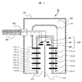
- FIG. 1 is a longitudinal sectional view of an electron beam generator of Example 1 according to one embodiment of the present invention.
- the electron beam generator 21 includes a metal housing 101 filled with an insulating gas 102, an electron gun 103 and a shield 112 disposed inside the metal housing 101, and a shield 112 disposed below the electron gun 103.
- accelerating electrodes 111-1 to n insulating materials 112-1 to n for insulating between them, resistors 113 to n electrically connecting between the accelerating electrodes, multicore cable 109 and bushing 108 Consists of
- the metal housing 101 may partially use a non-metallic member, but the inner surface is desirably made of metal or a conductive material.
- the insulating gas 102 may include sulfur hexafluoride, nitrogen, carbon dioxide, air, or various compounds containing carbon and fluorine.
- An electron source 104 , a suppressor electrode 105 and an extraction electrode 106 are arranged in a vacuum 107 in the electron gun 103 that constitutes the electron beam generator 21 .
- Below the electron gun 103 there are n acceleration electrodes 111-1 to n, insulating materials 112-1 to n for insulating between them, and resistors 113 to n for electrically connecting between the acceleration electrodes. .
- a high voltage is introduced into the metal housing 101 via a multi-core cable 109 and a bushing 108 connected to an external high voltage generator (not shown), and is applied to the electron gun 103 via wires in the insulating gas 102 .
- Electron source 104 , suppressor electrode 105 , extraction electrode 106 and shield 110 are powered.
- the shield 110 is made of a conductive member such as a metal material.
- Shield 110 is electrically connected to acceleration electrode 111-1, and power is supplied through shield 110 to acceleration electrode 111-1.
- the electron beam 114 can be generated by setting the potentials of the respective parts as follows: electron source 104 ⁇ leading electrode 106 ⁇ acceleration electrode 111-1 . . . acceleration electrode 111-n.
- An insulating paint may be applied to the inner surface of the shield 110 and/or the metal housing 101 .
- the insulating coating preferably has a volume resistivity of 10 12 ⁇ cm or more.
- non-linear resistance materials such as zinc oxide, silicon carbide, barium titanate, etc., whose resistivity depends on the electric field, can be added to the paint to improve insulation reliability due to the effect of relaxing the electric field when foreign matter adheres. is also desirable.
- An electron microscope is configured using the electron beam generator 21 having the above configuration. With the above configuration, by using the shield 110 for power supply from the bushing 108 to the acceleration electrode 111-1, dedicated high-potential wiring is not required, and insulation reliability is not lowered due to electric field concentration in the wiring. Furthermore, the effect of the insulating paint improves the insulation reliability, making it possible to realize a highly reliable insulation structure that does not cause dielectric breakdown.
- a charged particle beam device capable of realizing a highly reliable insulating structure.
- a shield having the same electric potential as that of the accelerating electrode is provided in the insulating gas space between the electron gun and the housing, and the shield is used for power supply from the bushing to the accelerating electrode, thereby providing a dedicated high electric potential. Therefore, it is possible to realize a highly reliable insulating structure that does not cause dielectric breakdown because it does not require wiring and does not cause deterioration in insulation reliability due to electric field concentration in wiring.
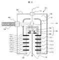
- FIG. 3 is a longitudinal sectional view of an electron beam generator of Example 2 according to another example of the present invention.
- the electron beam generator 21a according to this embodiment is characterized in that an electron gun shield 115 is provided between the shield 110 and the electron gun 103 in addition to the configuration of the first embodiment.
- the rest of the configuration is the same as that of the above-described first embodiment, and the same reference numerals are given to the same components as those of the first embodiment, and the description overlapping with that of the first embodiment will be omitted below.
- the electron gun shield 115 shown in FIG. 3 is electrically connected to any part of the electron gun 103 and has the same potential.
- FIG. 3 shows a configuration in which the potential is the same as that of the electron source 104, the configuration is not limited to this.
- the electron gun shield 115 may be electrically connected to the suppressor electrode 105, the extractor electrode 106, or other electrodes provided in the electron gun so as to have the same potential.
- Insulating paint may be applied to the inner surfaces of the shield 110, the metal housing 101 and/or the electron gun shield 115, as in the first embodiment described above.
- the insulating paint shown in the first embodiment may be applied.
- An electron microscope is configured using the electron beam generator 21a having the above configuration.
- the electron gun shield 115 having the same potential as any part of the electron gun 103 is provided between the electron gun 103 and the shield 110 having the same potential as that of the acceleration electrode 111-1. Therefore, it is possible to realize a highly reliable insulating structure that does not cause dielectric breakdown between the electron gun, the acceleration electrode, and the shield having the same potential.
- the shield having the same potential as any part of the electron gun is provided between the shield having the same potential as the acceleration electrode and the electron gun, thereby reducing wiring and terminals. It is possible to provide a charged particle beam device that can realize a highly reliable insulation structure that does not cause insulation breakdown between the electron gun, the acceleration electrode, and the shield of the same potential, because the insulation reliability does not deteriorate due to electric field concentration. becomes.
- FIG. 4 is a longitudinal sectional view of an electron beam generator of Example 3 according to another example of the present invention.
- the electron beam generator 21b according to the present embodiment differs from the first embodiment in that a plurality of bushings 108 and multicore cables 109 are provided.
- the rest of the configuration is the same as that of the above-described first embodiment, and the same reference numerals are given to the same components as those of the first embodiment, and the description overlapping with that of the first embodiment will be omitted below.
- the electron beam generator 21b is different from the electron beam generator 21 of the first embodiment described above in that the bushing 108-1 and the multicore cable 109-1, and the bushing 108-2 and the multicore cable 109 It has -2.
- bushing 108-1 and multicore cable 109-1, and bushing 108-2 and multicore cable 109-2 are arranged on opposite sides of the central axis.
- the bushing 108-1 and the multicore cable 109-1, and the bushing 108-2 and the multicore cable 109-2 are arranged to face each other.
- the arrangement of the bushing 108-1 and the multicore cable 109-1, and the arrangement of the bushing 108-2 and the multicore cable 109-2 are not limited to this.
- bushing 108-1 and multi-core cable 109-1, and bushing 108-2 and multi-core cable 109-2 may be arranged on top of metal housing 101.
- the electron beam generator 21 of the first embodiment the configuration including the bushing 108-1 and the multicore cable 109-1, and the bushing 108-2 and the multicore cable 109-2 has been described.
- the electron beam generator 21a of the second embodiment may be configured to include the bushing 108-1 and the multicore cable 109-1, and the bushing 108-2 and the multicore cable 109-2.
- An electron microscope is configured using the electron beam generator 21b having the above configuration.
- it is possible to realize a highly reliable insulation structure as in Embodiments 1 and 2, and it is possible to use a multi-core cable 109 with a small number of cores and a bushing 108, so that high-potential wiring can be separated by a sufficient distance. It becomes possible to hold and dispose, and a highly reliable insulating structure can be realized.
- Embodiments 1 and 2 in addition to the effects of Embodiments 1 and 2, it is possible to use a multi-core cable and bushing with a small number of cores, and it is possible to arrange high-potential wiring with a sufficient distance, Furthermore, it becomes possible to provide a charged particle beam device capable of realizing a highly reliable insulating structure.
- FIG. 5 is a longitudinal sectional view of an electron beam generator of Example 4 according to another example of the present invention.
- the electron beam generator 21c according to the present embodiment is different from that of the first embodiment in that a control wiring 117, a current introduction terminal 116, and an electron gun controller 118 are provided.
- the rest of the configuration is the same as that of the above-described first embodiment, and the same reference numerals are given to the same components as those of the first embodiment, and the description overlapping with that of the first embodiment will be omitted below.
- the electron beam generator 21c further includes a control wiring 117, a current introduction terminal 116, and an electron gun controller 118 in addition to the electron beam generator 21 of the first embodiment. It is preferable that one or more control wirings 117 and one or more current introduction terminals 116 are provided.
- the control wiring 117 may be an electric wire or an optical cable.
- the control wiring 117 is connected to the electron gun control device 118 through an opening provided in the shield 110, and transmits signals for controlling ON/OFF of the voltage and/or current of the electron gun 103.
- the electron beam generator 21 of the first embodiment is further provided with the control wiring 117, the current introduction terminal 116, and the electron gun control device 118, but the configuration is not limited to this.
- the electron beam generator 21a of the second embodiment or the electron beam generator 21b of the third embodiment may further include the control wiring 117, the current introduction terminal 116, and the electron gun controller 118.
- An electron microscope is configured using the electron beam generator 21c having the above configuration. With the above configuration, it is possible to realize a highly reliable insulating structure as in Embodiments 1, 2, and 3, and to realize ON/OFF control of the voltage and/or current of the electron gun 103. is.
- FIG. 6 is a longitudinal sectional view of an electron beam generator of Example 5 according to another example of the present invention.
- the potential of the shield 110 is not the same as that of the acceleration electrode 111-1, but is the same as that of any one of the electron guns 113. different from 1.
- the rest of the configuration is the same as that of the above-described first embodiment, and the same reference numerals are given to the same components as those of the first embodiment, and the description overlapping with that of the first embodiment will be omitted below.
- the potential of the shield 110 is not the same potential as that of the acceleration electrode 111-1, but is set to any potential of the electron gun 113. Therefore, the shield 110 is It is not electrically connected to the accelerating electrode 111-1, but is electrically connected to one of the electron guns 113 instead. Electric power is supplied to the acceleration electrode 111-1 through the multicore cable 109 and the bushing 108 by the acceleration tube power supply wiring 119 arranged inside the shield 110.
- the wiring 119 for power supply to the accelerating tube is insulated by keeping a sufficient distance from the shield 110 or by arranging an insulating material.
- the wiring 119 for power supply to the accelerating tube may be routed inside the vacuum 107 .
- the potential of the shield 110 shown in FIG. 5 is not the same as that of the acceleration electrode 111-1, but is the potential of one of the electron guns 113. Therefore, the shield 110 is electrically connected to the acceleration electrode 111-1. Instead, the configuration of electrically connecting to any one of the electron guns 113 and the configuration of supplying power to the acceleration electrode 111-1 through the acceleration tube power supply wiring 119 are similar to the electron beam generator 21a of the above-described second embodiment, It can also be applied to the electron beam generator 21b of the third embodiment and the electron beam generator 21c of the fourth embodiment.
- An electron microscope is configured using the electron beam generator 21d having the above configuration. With the above configuration, it is possible to realize a highly reliable insulation structure as in the second, third, or fourth embodiment. According to the present embodiment, it is possible to provide a charged particle beam apparatus capable of realizing a highly reliable insulating structure as in the second to fourth embodiments described above.
- the present invention is not limited to the above-described embodiments, and includes various modifications.
- the above-described embodiments have been described in detail in order to explain the present invention in an easy-to-understand manner, and are not necessarily limited to those having all the described configurations.
- SYMBOLS 1 Charged particle beam apparatus, 2... Housing, 3... Focusing lens control part, 4... Deflection control part, 5... Detection signal processing part, 6... Secondary electron detector, 7... Control device, 8... Display device, 9 external storage medium 10 recipe creating unit 12 image memory 21, 21a, 21b, 21c, 21d electron beam generator 22 focusing lens 23 deflector 24 objective lens 25 sample , 26... Sample holding unit 31... Write address control unit 32... Read address control unit 33... Display control unit 101... Metal housing 102... Insulating gas 103... Electron gun 104... Electron source 105...
- Suppressor electrode 106 Extraction electrode 107 Vacuum 108 Bushing 109 Multicore cable 110 Shield 111 Acceleration electrode 112 Insulator 113 Resistor 114 Electron beam 115 Electron gun Shield 116 Current introduction terminal 117 Control wiring 118 Electron gun control device 119 Accelerating tube power supply wiring
Landscapes
- Chemical & Material Sciences (AREA)
- Analytical Chemistry (AREA)
- Electron Sources, Ion Sources (AREA)
Priority Applications (3)
| Application Number | Priority Date | Filing Date | Title |
|---|---|---|---|
| US18/285,457 US12283452B2 (en) | 2021-04-15 | 2021-04-15 | Charged particle beam apparatus |
| JP2023514287A JP7494386B2 (ja) | 2021-04-15 | 2021-04-15 | 荷電粒子線装置 |
| PCT/JP2021/015638 WO2022219790A1 (ja) | 2021-04-15 | 2021-04-15 | 荷電粒子線装置 |
Applications Claiming Priority (1)
| Application Number | Priority Date | Filing Date | Title |
|---|---|---|---|
| PCT/JP2021/015638 WO2022219790A1 (ja) | 2021-04-15 | 2021-04-15 | 荷電粒子線装置 |
Publications (1)
| Publication Number | Publication Date |
|---|---|
| WO2022219790A1 true WO2022219790A1 (ja) | 2022-10-20 |
Family
ID=83640272
Family Applications (1)
| Application Number | Title | Priority Date | Filing Date |
|---|---|---|---|
| PCT/JP2021/015638 Ceased WO2022219790A1 (ja) | 2021-04-15 | 2021-04-15 | 荷電粒子線装置 |
Country Status (3)
| Country | Link |
|---|---|
| US (1) | US12283452B2 (https=) |
| JP (1) | JP7494386B2 (https=) |
| WO (1) | WO2022219790A1 (https=) |
Cited By (1)
| Publication number | Priority date | Publication date | Assignee | Title |
|---|---|---|---|---|
| WO2024247022A1 (ja) * | 2023-05-29 | 2024-12-05 | 株式会社日立ハイテク | 荷電粒子線装置 |
Citations (4)
| Publication number | Priority date | Publication date | Assignee | Title |
|---|---|---|---|---|
| JPS5568096A (en) * | 1978-11-16 | 1980-05-22 | Nippon Electron Optics Lab | Electron beam generator |
| JPS5948738U (ja) * | 1982-09-18 | 1984-03-31 | 日本電子株式会社 | イオン源 |
| JPS6199958U (https=) * | 1984-12-06 | 1986-06-26 | ||
| JPS61153999A (ja) * | 1984-12-26 | 1986-07-12 | 株式会社日立製作所 | 荷電粒子加速装置 |
Family Cites Families (3)
| Publication number | Priority date | Publication date | Assignee | Title |
|---|---|---|---|---|
| JPS5279758A (en) | 1975-12-26 | 1977-07-05 | Hitachi Ltd | Electronic gun |
| JP2014127296A (ja) | 2012-12-26 | 2014-07-07 | Nissin Electric Co Ltd | 電子線照射装置 |
| US20240170248A1 (en) * | 2022-11-22 | 2024-05-23 | Kamil Podhola | Particle beam system |
-
2021
- 2021-04-15 JP JP2023514287A patent/JP7494386B2/ja active Active
- 2021-04-15 US US18/285,457 patent/US12283452B2/en active Active
- 2021-04-15 WO PCT/JP2021/015638 patent/WO2022219790A1/ja not_active Ceased
Patent Citations (4)
| Publication number | Priority date | Publication date | Assignee | Title |
|---|---|---|---|---|
| JPS5568096A (en) * | 1978-11-16 | 1980-05-22 | Nippon Electron Optics Lab | Electron beam generator |
| JPS5948738U (ja) * | 1982-09-18 | 1984-03-31 | 日本電子株式会社 | イオン源 |
| JPS6199958U (https=) * | 1984-12-06 | 1986-06-26 | ||
| JPS61153999A (ja) * | 1984-12-26 | 1986-07-12 | 株式会社日立製作所 | 荷電粒子加速装置 |
Cited By (1)
| Publication number | Priority date | Publication date | Assignee | Title |
|---|---|---|---|---|
| WO2024247022A1 (ja) * | 2023-05-29 | 2024-12-05 | 株式会社日立ハイテク | 荷電粒子線装置 |
Also Published As
| Publication number | Publication date |
|---|---|
| JPWO2022219790A1 (https=) | 2022-10-20 |
| JP7494386B2 (ja) | 2024-06-03 |
| US20250079112A1 (en) | 2025-03-06 |
| US12283452B2 (en) | 2025-04-22 |
Similar Documents
| Publication | Publication Date | Title |
|---|---|---|
| JP6420444B1 (ja) | 電子集束改善用x線管 | |
| KR100496496B1 (ko) | 하전 입자 빔 장치용 광 컬럼 | |
| US4274035A (en) | Field emission electron gun | |
| JP2007109675A (ja) | 単色分光計用の固定ダイヤフラムからなる粒子光学装置 | |
| JP7494386B2 (ja) | 荷電粒子線装置 | |
| US6693282B1 (en) | Particle-optical apparatus including a particle source that can be switched between high brightness and large beam current | |
| JP2019003863A (ja) | 電子ビーム装置、ならびに、これを備えるx線発生装置および走査電子顕微鏡 | |
| WO2010001953A1 (ja) | 電子源装置、イオン源装置、及び荷電粒子源装置 | |
| US6657193B2 (en) | Scanning electron microscope | |
| US20090295269A1 (en) | Electron beam generator | |
| JPH04233146A (ja) | 帯電粒子ビーム装置 | |
| JP4246372B2 (ja) | 電子ビーム生成装置及び電子ビーム露光装置 | |
| US11139139B2 (en) | Charged particle beam generator and charged particle beam apparatus | |
| JP3485888B2 (ja) | 電子ビーム描画装置及びそれを用いて作製された半導体デバイス | |
| JP2002270125A (ja) | 高電圧電気機器 | |
| US3303345A (en) | Image amplifier with magnification grid | |
| US6740888B2 (en) | Electron beam apparatus | |
| WO2002045123A1 (fr) | Dispositif de production de faisceau d'electrons, et dispositif de test | |
| US3938001A (en) | Protection circuit for electron gun | |
| WO2020213109A1 (ja) | 電子源、及び荷電粒子線装置 | |
| WO2024247022A1 (ja) | 荷電粒子線装置 | |
| JPS6340017B2 (https=) | ||
| US3358173A (en) | Beam generating system for electron tubes with a high breakdown strength | |
| KR830000415B1 (ko) | 전계방사형 전자총 | |
| JP2930701B2 (ja) | 電界放出型電子銃 |
Legal Events
| Date | Code | Title | Description |
|---|---|---|---|
| 121 | Ep: the epo has been informed by wipo that ep was designated in this application |
Ref document number: 21936986 Country of ref document: EP Kind code of ref document: A1 |
|
| ENP | Entry into the national phase |
Ref document number: 2023514287 Country of ref document: JP Kind code of ref document: A |
|
| WWE | Wipo information: entry into national phase |
Ref document number: 18285457 Country of ref document: US |
|
| NENP | Non-entry into the national phase |
Ref country code: DE |
|
| 122 | Ep: pct application non-entry in european phase |
Ref document number: 21936986 Country of ref document: EP Kind code of ref document: A1 |
|
| WWP | Wipo information: published in national office |
Ref document number: 18285457 Country of ref document: US |
|
| WWG | Wipo information: grant in national office |
Ref document number: 18285457 Country of ref document: US |