WO2022202015A1 - 半導体装置、半導体装置製造方法 - Google Patents
半導体装置、半導体装置製造方法 Download PDFInfo
- Publication number
- WO2022202015A1 WO2022202015A1 PCT/JP2022/006670 JP2022006670W WO2022202015A1 WO 2022202015 A1 WO2022202015 A1 WO 2022202015A1 JP 2022006670 W JP2022006670 W JP 2022006670W WO 2022202015 A1 WO2022202015 A1 WO 2022202015A1
- Authority
- WO
- WIPO (PCT)
- Prior art keywords
- wirings
- wiring
- semiconductor device
- semiconductor substrate
- rewiring layer
- Prior art date
- Legal status (The legal status is an assumption and is not a legal conclusion. Google has not performed a legal analysis and makes no representation as to the accuracy of the status listed.)
- Ceased
Links
Images









Classifications
-
- H—ELECTRICITY
- H10—SEMICONDUCTOR DEVICES; ELECTRIC SOLID-STATE DEVICES NOT OTHERWISE PROVIDED FOR
- H10W—GENERIC PACKAGES, INTERCONNECTIONS, CONNECTORS OR OTHER CONSTRUCTIONAL DETAILS OF DEVICES COVERED BY CLASS H10
- H10W72/00—Interconnections or connectors in packages
- H10W72/20—Bump connectors, e.g. solder bumps or copper pillars; Dummy bumps; Thermal bumps
-
- H—ELECTRICITY
- H10—SEMICONDUCTOR DEVICES; ELECTRIC SOLID-STATE DEVICES NOT OTHERWISE PROVIDED FOR
- H10W—GENERIC PACKAGES, INTERCONNECTIONS, CONNECTORS OR OTHER CONSTRUCTIONAL DETAILS OF DEVICES COVERED BY CLASS H10
- H10W20/00—Interconnections in chips, wafers or substrates
- H10W20/20—Interconnections within wafers or substrates, e.g. through-silicon vias [TSV]
-
- H—ELECTRICITY
- H10—SEMICONDUCTOR DEVICES; ELECTRIC SOLID-STATE DEVICES NOT OTHERWISE PROVIDED FOR
- H10W—GENERIC PACKAGES, INTERCONNECTIONS, CONNECTORS OR OTHER CONSTRUCTIONAL DETAILS OF DEVICES COVERED BY CLASS H10
- H10W20/00—Interconnections in chips, wafers or substrates
- H10W20/40—Interconnections external to wafers or substrates, e.g. back-end-of-line [BEOL] metallisations or vias connecting to gate electrodes
- H10W20/41—Interconnections external to wafers or substrates, e.g. back-end-of-line [BEOL] metallisations or vias connecting to gate electrodes characterised by their conductive parts
- H10W20/43—Layouts of interconnections
-
- H—ELECTRICITY
- H10—SEMICONDUCTOR DEVICES; ELECTRIC SOLID-STATE DEVICES NOT OTHERWISE PROVIDED FOR
- H10W—GENERIC PACKAGES, INTERCONNECTIONS, CONNECTORS OR OTHER CONSTRUCTIONAL DETAILS OF DEVICES COVERED BY CLASS H10
- H10W72/00—Interconnections or connectors in packages
- H10W72/90—Bond pads, in general
-
- H—ELECTRICITY
- H10—SEMICONDUCTOR DEVICES; ELECTRIC SOLID-STATE DEVICES NOT OTHERWISE PROVIDED FOR
- H10W—GENERIC PACKAGES, INTERCONNECTIONS, CONNECTORS OR OTHER CONSTRUCTIONAL DETAILS OF DEVICES COVERED BY CLASS H10
- H10W70/00—Package substrates; Interposers; Redistribution layers [RDL]
- H10W70/60—Insulating or insulated package substrates; Interposers; Redistribution layers
-
- H—ELECTRICITY
- H10—SEMICONDUCTOR DEVICES; ELECTRIC SOLID-STATE DEVICES NOT OTHERWISE PROVIDED FOR
- H10W—GENERIC PACKAGES, INTERCONNECTIONS, CONNECTORS OR OTHER CONSTRUCTIONAL DETAILS OF DEVICES COVERED BY CLASS H10
- H10W70/00—Package substrates; Interposers; Redistribution layers [RDL]
- H10W70/60—Insulating or insulated package substrates; Interposers; Redistribution layers
- H10W70/62—Insulating or insulated package substrates; Interposers; Redistribution layers characterised by their interconnections
- H10W70/65—Shapes or dispositions of interconnections
-
- H—ELECTRICITY
- H10—SEMICONDUCTOR DEVICES; ELECTRIC SOLID-STATE DEVICES NOT OTHERWISE PROVIDED FOR
- H10W—GENERIC PACKAGES, INTERCONNECTIONS, CONNECTORS OR OTHER CONSTRUCTIONAL DETAILS OF DEVICES COVERED BY CLASS H10
- H10W70/00—Package substrates; Interposers; Redistribution layers [RDL]
- H10W70/60—Insulating or insulated package substrates; Interposers; Redistribution layers
- H10W70/67—Insulating or insulated package substrates; Interposers; Redistribution layers characterised by their insulating layers or insulating parts
- H10W70/68—Shapes or dispositions thereof
-
- H—ELECTRICITY
- H10—SEMICONDUCTOR DEVICES; ELECTRIC SOLID-STATE DEVICES NOT OTHERWISE PROVIDED FOR
- H10W—GENERIC PACKAGES, INTERCONNECTIONS, CONNECTORS OR OTHER CONSTRUCTIONAL DETAILS OF DEVICES COVERED BY CLASS H10
- H10W90/00—Package configurations
- H10W90/701—Package configurations characterised by the relative positions of pads or connectors relative to package parts
- H10W90/721—Package configurations characterised by the relative positions of pads or connectors relative to package parts of bump connectors
- H10W90/722—Package configurations characterised by the relative positions of pads or connectors relative to package parts of bump connectors between stacked chips
Definitions
- the present technology relates to a semiconductor device having a rewiring layer and a semiconductor device manufacturing method.
- RDL redistribution layer
- Patent Document 1 discloses a technique for reducing the capacitance by providing a gap between wirings.
- This technology was created in view of such problems, and aims to reliably form gaps between wiring.
- a semiconductor device includes a semiconductor substrate, a wiring layer having electrode pads and formed on a first surface of the semiconductor substrate, and wiring electrically connected to the electrode pads through vias.
- a rewiring layer formed on a second surface opposite to the first surface of the semiconductor substrate; a protective film formed on a surface of the rewiring layer opposite to the semiconductor substrate; a partition formed of a material and arranged between the wirings in the rewiring layer, wherein the partitions and the gaps are alternately formed between the wirings in the direction in which the wirings extend. Thereby, a gap is formed by the two wirings and the two partitions.
- a wiring layer having electrode pads is formed on a first surface, and a rewiring layer having wiring electrically connected to the electrode pads through vias is formed on the first surface.
- partitions and gaps are alternately formed between the wirings in the rewiring layer in the direction in which the wirings extend.
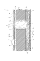
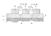
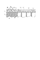
- FIG. 1 is a cross-sectional view showing an example of a semiconductor device
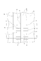
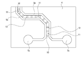
- FIG. FIG. 3 is a diagram showing an example of a rewiring layer together with FIG. 3, and this diagram is a plan view of the back side.
- FIG. 4 is a cross-sectional view of an example of a rewiring layer;
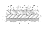
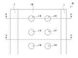
- FIG. 4 is a plan view of the rear surface side showing a state in which a partition portion and a gap are formed between wirings of parallel wirings;
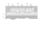
- FIG. 5 is a cross-sectional view taken along line BB of FIG. 4;
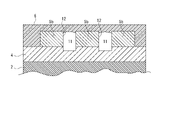
- FIG. 5 is a cross-sectional view taken along line CC of FIG. 4; It is sectional drawing which expands and shows parallel wiring, a partition part, and a space
- FIG. 4 is a cross-sectional view showing a state in which a rewiring layer is formed;
- FIG. 4 is a cross-sectional view showing a state in which a recessed groove is formed;
- FIG. 4 is a cross-sectional view showing a state in which an insulating film is formed;
- FIG. 4 is a cross-sectional view showing a state in which parallel wirings are exposed by CMP processing;
- FIG. 4 is a plan view of the back side showing a state in which a resist is applied;
- FIG. 13 is a cross-sectional view taken along line DD of FIG. 12;
- FIG. 4 is a plan view of the back side showing a state in which an insulating film is removed;
- FIG. 15 is a cross-sectional view taken along line EE of FIG.
- FIG. 14 is a cross-sectional view taken along line FF of FIG. 14;
- FIG. 4 is a plan view of the back side showing a state where the resist is removed;
- FIG. 18 is a cross-sectional view taken along line GG of FIG. 17;
- FIG. 18 is a cross-sectional view taken along line HH of FIG. 17;
- FIG. 11 is a plan view of the back side showing a state in which a resist is applied in the first modified example;
- FIG. 21 is a cross-sectional view taken along line JJ of FIG. 20;
- FIG. 11 is a plan view of the rear surface side showing a state in which the insulating film is removed in the first modified example;
- FIG. 23 is a cross-sectional view taken along line KK of FIG. 22;
- FIG. 11 is a plan view of the back surface side showing a state in which the resist is removed in the first modified example;
- FIG. 11 is a plan view of the back side showing a state in which a resist is applied in a second modified example;
- FIG. 26 is a cross-sectional view taken along line PP of FIG. 25;
- FIG. 11 is a plan view of the rear surface side showing a state in which the insulating film is removed in the second modified example;
- FIG. 28 is a cross-sectional view taken along line RR of FIG. 27;
- FIG. 12 is a plan view of the back surface side showing a state in which the resist is removed in the second modified example;
- FIG. 11B is a diagram for explaining a third modification, and is a plan view of the back side showing a state in which the arrangement interval of the partitions is changed according to the distance between the wirings.
- FIG. 12B is a diagram for explaining a fourth modification, and is a plan view of the back side showing a state in which a partition portion is formed between wirings of parallel wirings formed on a non-straight line.
- FIG. 10 is a cross-sectional view showing a state in which the present technology is applied to a semiconductor device as an image sensor;
- the semiconductor device 1 is manufactured by, for example, WCSP (Wafer level Chip Size Package) technology.
- WCSP Wafer level Chip Size Package
- a cross section of an example of the configuration of a semiconductor device 1 is shown in FIG.
- the semiconductor device 1 includes a semiconductor substrate 2, a wiring layer 3 laminated on the front surface 2a of the semiconductor substrate 2, an insulating resin film 4 laminated on the back surface 2b of the semiconductor substrate 2, and a redistribution layer (RDL). 5 and a protective film 6 .
- RDL redistribution layer
- the semiconductor substrate 2 is, for example, a silicon layer, and is formed with a certain thickness to improve the strength of the semiconductor wafer.
- Various semiconductor elements EL such as transistors are formed on the surface 2 a of the semiconductor substrate 2 .
- a through hole 2c is formed at a predetermined position in the semiconductor substrate 2. As shown in FIG.
- the wiring layer 3 is formed of a plurality of layers covering the surface 2a of the semiconductor substrate 2 on which the transistors are formed.
- the wiring layer 3 is formed by alternately laminating a first layer 3a made of an insulating material and a second layer 3b having a wiring pattern formed thereon.
- the simplest structure of the wiring layer 3 is a three-layer structure consisting of two first layers 3a and a second layer 3b formed therebetween.
- the wiring layer 3 in the example shown in FIG. 1 has a seven-layer structure consisting of four first layers 3a and three second layers 3b.
- vias (not shown) for electrically connecting the second layers 3b are formed in the stacking direction.
- the second layer 3b included in the wiring layer 3 is formed with electrode pads 7 for electrical connection with an external device.
- the electrode pads 7 are formed on the second layer 3b closest to the semiconductor substrate 2 among the three second layers 3b.
- the wiring layer 3 is formed with a recess 3c that is continuous with the through hole 2c of the semiconductor substrate 2. As shown in FIG. Recess 3c is formed so that at least part of electrode pad 7 is exposed.
- the through holes 2c and the recesses 3c are holes 8 that are bored in the semiconductor substrate 2 and the wiring layers 3 in the stacking direction.
- the electrode pads 7 and the hole portions 8 are provided at the same position when viewed from the stacking direction of each layer. That is, the electrode pads 7 are partially exposed on the bottom surface of the hole 8 .
- the insulating resin film 4 is a layer provided to avoid unnecessary electrical connection between the semiconductor substrate 2 and the rewiring layer 5, and is made of an organic material such as polyimide, silicon, acrylic, epoxy, SOC (Spin-on Carbon), or the like. Membrane.
- the insulating resin film 4 is formed not only on the back surface 2 b of the semiconductor substrate 2 but also on the inner peripheral surface of the hole 8 .
- the rewiring layer 5 is formed on the inner peripheral surface of the insulating resin film 4 formed over the inner peripheral surface of the hole 8 and at predetermined positions on the surface of the insulating resin film 4 formed on the surface 2 a of the semiconductor substrate 2 . It is a layer electrically connected to the electrode pad 7 by being formed in the second layer.
- the portion formed on the inner peripheral surface of the insulating resin film 4 formed over the inner peripheral surface of the hole 8 serves as a through electrode TSV.
- the rewiring layer 5 formed at a predetermined position on the surface of the insulating resin film 4 is composed of a single wiring 5a, a parallel wiring 5b, a connection pad 5c, and the like.
- connection pads 5c on which metal bumps 9 such as solder are formed are formed at predetermined positions.
- the parallel wirings 5b are two or more wirings extending in substantially the same direction with an inter-wiring distance of less than a certain value.
- the wiring may meander. In order for the semiconductor device 1 to operate at high speed, the inter-wiring capacitance of the parallel wiring 5b becomes a problem.
- a single wire is one in which there are no other wires arranged in parallel.
- the rewiring layer 5 is made of titanium (Ti), copper (Cu), tantalum (Ta), nickel (Ni), tungsten (W), or the like.
- partitions 10 and gaps 11 are alternately formed between the wirings of the parallel wirings 5b.
- the protective film 6 is a layer formed on the back side of the rewiring layer 5 .
- the protective film 6 is made of an insulating resin material or the like, and is formed by a spin coating method.
- FIG. 2 shows the rewiring layer 5 with a dashed line and is a view seen from the back side.
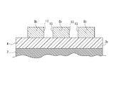
- FIG. 3 is a longitudinal sectional view taken along line AA in FIG. 2.
- connection pad 5c As shown in FIG. 2, part of the connection pad 5c is exposed on the back side, but the single wiring 5a and the parallel wiring 5b are covered with the protective film 6 and cannot be visually recognized.
- a gap 11 is formed between the wirings of the parallel wirings 5b.
- the gap 11 is formed by preventing the protective film 6 from entering between the wirings of the parallel wirings 5b. Further, the gap 11 is formed by scraping not only between the wirings of the parallel wirings 5b but also the back side of the insulating resin film 4. As shown in FIG. 3,
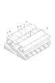
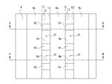
- FIG. 4 shows the partition portion 10 forming the gap 11 .
- FIG. 4 is a diagram in which the protective film 6 formed on the rear surface side of the rewiring layer 5 is not shown. Partitions 10 and gaps 11 are alternately formed between the wirings of the parallel wirings 5b along the direction in which the parallel wirings 5b extend.
- the material of the partition part 10 may be organic or inorganic.
- the partition part 10 is made of SiO 2 , SiON, an organic resin material, or the like.
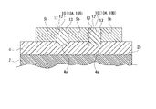
- FIG. 5 shows a cross-sectional view taken along the line BB in FIG. 4 and a cross-sectional view of a portion where the partition portion 10 is formed.
- the partition part 10 has a substantially rectangular parallelepiped shape and is arranged on the bottom surface of the groove part 12 between the wirings of the parallel wirings 5b.
- a gap 11 is formed by forming the partitions 10 at regular intervals in the grooves 12 between the wirings of the parallel wirings 5b.
- FIG. 6 shows a cross-sectional view taken along the line CC of FIG. 4 and a cross-sectional view of the portion where the void 11 is formed.
- the gap 11 is formed by preventing the protective film 6 from entering the groove 12 .
- Inter-wiring capacitance > Inter-wiring capacitance of the parallel wiring 5b will be described.
- Inter-wiring capacitance Q can be expressed by the following equation (1) using capacitance C and voltage V.
- the capacitance C can be expressed by the following equation (2) using the dielectric constant ⁇ , the side area S, and the distance d between the wirings.
- the side area S is the area of the side surface 13 of the parallel wiring 5b.
- the inter-wiring distance d is the distance between the facing surfaces of the parallel wiring 5b (see FIG. 7).
- the dielectric constant ⁇ differs depending on the material. Specifically, it can be represented by the following formula (3).
- ⁇ 0 represents the permittivity of vacuum
- ⁇ r represents the relative permittivity, which is the ratio of permittivity to vacuum.
- the protective film 6 enters the groove portion 12 , so that the side surfaces 13 come into contact with the protective film 6 over the entire surface.
- the dielectric constant ⁇ r of the material forming the protective film 6 is higher than the dielectric constant of vacuum or air. Therefore, since the dielectric constant ⁇ is higher than that of vacuum or air, the electrostatic capacitance C is increased and the inter-wiring capacitance Q is also increased.
- This effect increases as the contact area between the side surface 13 and the gap 11 increases, that is, as the contact area between the side surface 13 and the partition 10 decreases.
- FIG. 8 shows a state in which the insulating resin film 4 is formed on the rear surface 2b of the semiconductor substrate 2, and parallel wiring 5b of the rewiring layer 5 is formed on the rear surface side. That is, when the state shown in FIG. 8 is viewed from the back side, the wiring pattern as the rewiring layer 5 is formed on the surface of the insulating resin film 4 . Also, in this example, three parallel wirings 5b are taken as an example.
- wiring layer 3 formed on the surface 2a of the semiconductor substrate 2 is not shown in each figure after FIG.
- recessed grooves 4a are formed in the insulating resin film 4 so as to open to the rear surface side and sideways.
- the concave groove 4a is formed so as to be continuous with the side surface 13 of the parallel wiring 5b. Further, the side surface 13 of the parallel wiring 5b and the concave groove 4a of the insulating resin film 4 are formed as a groove portion 12. As shown in FIG. This process is realized by, for example, an etching process.
- a film forming process is performed to form an insulating film 14 such as SiO 2 , SiON, or an organic resin material.
- the insulating film 14 is formed so as to enter the trench 12 between the side surfaces 13 of the parallel wiring 5b.
- a CMP (Chemical Mechanical Polishing) process is performed on the back side of the insulating film 14 to expose the parallel wiring 5b.
- the height position of the back side of the insulating film 14 with respect to the semiconductor substrate 2 and the height position of the back side of the parallel wiring 5b with respect to the semiconductor substrate 2 are matched.
- FIG. 12 shows a plan view from the rear surface side with the resist 15 applied
- FIG. 13 shows a cross-sectional view taken along line DD of FIG.
- strip-shaped resists 15 whose longitudinal direction is the direction orthogonal to the parallel wirings 5b are applied at regular intervals along the extending direction of the parallel wirings 5b.
- FIG. 14 shows a plan view from the back side with the insulating film 14 removed.
- 15 is a sectional view taken along line EE in FIG. 14, and a sectional view taken along line FF in FIG. 14 is shown in FIG.
- the insulating film 14 protected by the resist 15 remains as the partition 10 in the trench 12 .
- the insulating film 14 not protected by the resist 15 is removed to form the void 11 .
- FIG. 17 is a plan view of the back side of the state after the resist 15 is removed
- FIG. 18 is a cross-sectional view taken along line GG in FIG. 17
- FIG. 19 is a cross-sectional view taken along line HH in FIG. show.
- the partitions 10 are formed in the grooves 12 at regular intervals in the direction in which the parallel wirings 5b extend. Further, as shown in FIGS. 17 and 19 , gaps 11 are formed between the partitions 10 in the grooves 12 .
- a protective film 6 is formed on the rear surface side of the rewiring layer 5 by spin coating in a state in which the partitions 10 and the gaps 11 are alternately formed in the grooves 12 in the direction in which the parallel wirings 5b extend.
- the chemical solution enters the groove portion 12 when the flowing direction of the chemical solution forming the protective film 6 and the extending direction of the parallel wiring 5b match. Therefore, a gap may not be formed between the parallel wirings 5b, and the inter-wiring capacitance Q of the parallel wirings 5b cannot be reduced.
- the partition 10 and the gap 11 are both rectangular parallelepipeds.
- the gap 11 is not a simple groove but has a rectangular parallelepiped shape, it is difficult for the chemical solution to enter the gap 11 regardless of the flow direction of the chemical solution used in the spin coating method, and as shown in FIG.
- the air gap 11 can be stably formed at . Thereby, the inter-wiring capacitance Q of the parallel wiring 5b can be reduced.
- dynamic coating is more advantageous than static coating.
- dynamic application it is possible to make it difficult for the medicine to enter the void 11, to ensure the state in which the void 11 is formed, and to increase the volume of the void 11 that can be formed. Therefore, the inter-wiring capacitance Q of the parallel wiring 5b can be efficiently reduced.
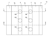
- a first modification is an example in which a columnar partition 10A is formed with the thickness direction of the semiconductor substrate 2 being the axial direction in the groove 12 formed between the parallel wirings 5b.
- the lithography process is performed.
- circular resists 15A are applied on the rear surface side of the insulating film 14 that has entered the groove 12 and are spaced apart at regular intervals in the direction in which the parallel wirings 5b extend.
- FIG. 20 shows a plan view of the back side with the resist 15A applied
- FIG. 21 shows a cross-sectional view taken along line JJ in FIG.
- FIG. 22 shows a plan view of the back side of the semiconductor device 1A after etching
- FIG. 23 shows a cross-sectional view taken along line KK of FIG.
- cylindrical partitions 10A are formed at regular intervals in the direction in which the parallel wirings 5b extend in the groove 12. As shown in FIG. 1
- FIG. 24 shows a plan view of the back side of the state where the resist 15A is removed. 24 is the same as the previous FIG. 18, and the sectional view along the MM line of FIG. 24 is the same as the previous FIG.
- a gap 11A is formed between the cylindrical partitions 10A arranged in the groove 12. As shown in FIGS. 24 and 19, a gap 11A is formed between the cylindrical partitions 10A arranged in the groove 12. As shown in FIGS. 24 and 19, a gap 11A is formed between the cylindrical partitions 10A arranged in the groove 12. As shown in FIGS. 24 and 19, a gap 11A is formed between the cylindrical partitions 10A arranged in the groove 12. As shown in FIGS.
- the cylindrical partition 10A is in contact with the side surface 13 of the parallel wiring 5b. Therefore, since most of the side surface 13 of the parallel wiring 5b is adjacent to the air gap 11A, the inter-wiring capacitance Q can be further reduced.
- Second modification> is an example in which a cylindrical hole formed in the groove portion 12 is used as the void 11 .
- the steps up to formation of the resist 15 are the same. 8 to 11 are the same steps, and description thereof will be omitted.
- the lithography process is performed.
- the resist 15B is applied to the rear surface of the insulating film 14 that has entered the groove 12 so that the insulating film 14 is removed in a columnar shape at regular intervals in the direction in which the parallel wiring 5b extends.
- FIG. 25 shows a plan view of the back side of the semiconductor device 1B coated with the resist 15B. Note that the cross-sectional view taken along line NN in FIG. 25 is the same as in FIG. FIG. 26 shows a cross-sectional view taken along line PP of FIG.
- FIG. 27 shows a plan view of the back side of the semiconductor device 1B after etching. 27 is the same as FIG. 15 above. Also, FIG. 28 shows a cross-sectional view taken along line RR of FIG.
- cylindrical hole portions 16 are formed at regular intervals in the direction in which the parallel wiring 5b extends in the groove portion 12 .
- FIG. 29 shows a plan view of the back side of the state where the resist 15B is removed. 29 is the same as the previous FIG. 18, and the TT line of FIG. 29 is the same as the previous FIG.
- columnar holes 16 are formed as gaps 11B at regular intervals in the grooves 12, and the insulating film 14 remains as partitions 10B in the gaps.
- the chemical solution may enter the gaps 11A and disappear in the first modification and the like.
- the opening of the gap 11B is made small, so that the gap 11B can be stably formed.
- a third modification is an example in which the distance between the partitions 10, that is, the length of the gap 11 in the direction in which the parallel wirings 5b extend is changed according to the length of the distance d between the wirings of the parallel wirings 5b.
- FIG. 30 is a plan view on the back side. Note that the protective film 6 is not shown in FIG.
- a first parallel wiring 5b1 with an inter-wiring distance d1 and a second parallel wiring 5b2 with an inter-wiring distance d2 are formed on the back surface side of the insulating resin film 4.
- FIG. The distance d1 between wires is set shorter than the distance d2 between wires. That is, the first parallel wiring 5b1 is formed as a relatively finer wiring pattern than the second parallel wiring 5b2.
- the capacitance C of the first parallel wiring 5b1 is larger than that of the second parallel wiring 5b2 because the variable d in the above equation (2) is smaller than that of the second parallel wiring 5b2. Therefore, in order to reduce the capacitance C, the air gap 11 having a small relative dielectric constant ⁇ r and the side surface 13 of the first parallel wiring 5b1 are arranged so that the average relative dielectric constant ⁇ r of the first parallel wiring 5b1 becomes small. so that the contact area of
- the finer first parallel wiring 5b1 is more fine than the second parallel wiring 5b2. It is preferable to widen the arrangement interval of the partitions 10 .
- miniaturization of the parallel wirings 5b is synonymous with shortening the distance d between the wirings, so that the liquid agent is less likely to enter the gaps 11.
- FIG. Therefore, even if the arrangement interval of the partition part 10 is widened in consideration of that amount, the protective film 6 can be formed in a state where the gap 11 is formed without any problem without the liquid agent entering the gap 11. ⁇
- a fourth modified example is an example in which adjacent partition portions 10 in the groove portion 12 of the parallel wiring 5b are non-parallel. A specific description will be given with reference to FIG.
- the illustrated parallel wiring 5b is formed in a non-linear shape when viewed as a whole by connecting straight lines extending in different directions.
- the parallel wirings 5b formed by curved lines and the parallel wirings 5b formed by two or more straight lines are configured such that the partitions 10 formed in the grooves 12 are non-parallel. That is, the partition portion 10 is formed so that the longitudinal direction is perpendicular to the direction in which the adjacent parallel wirings 5b extend.
- the partitions 10 when the partitions 10 are arranged so as to be spaced apart at a predetermined interval, the partitions 10 may be formed so as to be adjacent to the parallel wiring 5b on the inner circumference side at a predetermined interval, The partition part 10 may be formed so as to be adjacent to the parallel wiring 5b on the outer peripheral side at a predetermined interval.
- FIG. 32 An image sensor device is shown in FIG. 32 as an example. 32, illustration of the wiring layer 3 formed on the surface 2a side of the semiconductor substrate 2 is omitted.
- photoelectric conversion elements 17 are provided in a two-dimensional array in the central portion of the semiconductor substrate 2, and an insulating resin film 4 and a protective film 6 are formed on the back side thereof.
- a photoelectric conversion element 17 is not formed on the outer peripheral portion of the semiconductor substrate 2 , and an insulating resin film 4 , a rewiring layer 5 and a protective film 6 are formed on the back side of the semiconductor substrate 2 .
- the partitions 10 and the gaps 11 as described above are alternately formed.
- the rewiring layer 5 by forming the rewiring layer 5, the partition portion 10, and the gap 11 in the portion of the semiconductor substrate 2 where the photoelectric conversion element 17 is not formed, the incidence of light to the photoelectric conversion element 17 is not hindered. , the inter-wiring capacitance Q of the parallel wiring 5b can be reduced.
- the semiconductor device 1 (1A, 1B) includes the semiconductor substrate 2 and the wiring layer 3 having the electrode pads 7 and formed on the first surface (surface 2a) of the semiconductor substrate 2. and a wiring electrically connected to the electrode pad 7 via a via (through electrode TSV) and formed on the second surface (back surface 2b) opposite to the first surface of the semiconductor substrate 2
- the protective film 6 can be formed while the gap 11 is secured.
- the inter-wiring capacitance Q between the two wirings can be reduced.
- it is effective when forming the protective film 6 using the spin coating method. That is, it is possible to inevitably form the gap 11 between the wirings simply by forming the protective film 6 by the spin coating method as usual. Further, by reducing the inter-wiring capacitance Q, it becomes possible to manufacture the semiconductor device 1 capable of high-speed operation.
- the insulating material used to form the partitions 10 (10A, 10B) may be any one of SiOx, SiOxNy, and insulating organic resin.
- x and y are variables representing natural numbers.
- two wirings two and two wirings (two second parallel wirings 5b2) having a second inter-wiring distance d2 are formed, and the first inter-wiring distance d1 is the second
- the distance between the partitions 10 arranged between the two wires having the first inter-wiring distance d1 which is shorter than the inter-wiring distance d2 and adjacent to each other in the direction in which the wires extend is equal to the second inter-wiring distance. It may be larger than the interval between the partitions 10 arranged between two wirings of d2 and adjacent to each other in the direction in which the wirings extend.
- the interval between the partitions 10 (10A, 10B) arranged and adjacent to each other in the direction in which the wiring extends may be increased.
- the contact area with the partitioning portion 10 is made smaller for the two wirings whose inter-wiring capacitance Q is large due to the short inter-wiring distance d. Therefore, the effect of reducing the inter-wiring capacitance Q can be maintained.
- the stacking direction of the rewiring layer 5 with respect to the semiconductor substrate 2 is the axial direction of the partition portion 10A. It may be cylindrical in shape. That is, the side surface of the cylindrical partition 10A is in contact with the side surface 13 of the parallel wiring 5b. As a result, the contact area between the wiring and the partition portion 10A is further reduced, and the inter-wiring capacitance Q can be further reduced.
- the partition portion 10 may have a rectangular parallelepiped shape.
- the space 11 adjacent to the partition portion 10 is also a rectangular parallelepiped space. Therefore, the area where the wiring (parallel wiring 5b) is adjacent to the air gap 11 is increased, and the inter-wiring capacitance Q can be reduced.
- the gap 11B of the semiconductor device 1B is the hole 16 formed in the insulating material between the wirings (between the parallel wirings 5b). may As a result, hole-like gaps 11B are formed between the partitions 10B. Therefore, it is possible to reduce the inter-wiring capacitance Q for the two wirings arranged on both sides of the air gap 11B.
- the insulating resin film 4 is formed between the semiconductor substrate 2 and the rewiring layer 5, and the gap 11 (11A, 11B) may be formed as a space reaching the inside of the insulating resin film 4, that is, as a space including a recess (recess groove 4a) formed in the insulating resin film 4.
- FIG. Thereby, a gap 11 deeper than the height of the wiring (parallel wiring 5b) is formed. Therefore, since the side surfaces 13 of the two wirings can be reliably placed adjacent to the gap, the inter-wiring capacitance Q can be reliably reduced.
- ion migration can be reduced.
- the photoelectric conversion elements 17 that perform photoelectric conversion may be formed in a two-dimensional array on the semiconductor substrate 2 .
- a gap 11 is formed between the wirings of the rewiring layer 5 in the semiconductor device 1 such as an image sensor. Therefore, the inter-wiring capacitance Q can be reduced, which is suitable for high-speed driving of the image sensor.
- the method for manufacturing a semiconductor device includes a semiconductor substrate 2, a wiring layer 3 having an electrode pad 7 and formed on a first surface (surface 2a) of the semiconductor substrate 2, and vias (through electrodes TSV). a rewiring layer 5 having a wiring electrically connected to the electrode pad 7 and formed on the second surface (back surface 2b) of the semiconductor substrate 2 opposite to the first surface; A semiconductor device 1 comprising a protective film 6 formed on a surface opposite to a semiconductor substrate 2, and a partition portion 10 formed of an insulating material and arranged between wirings (between parallel wirings 5b) in a rewiring layer 5.
- partitions 10 and gaps 11 are alternately formed between wirings in the direction in which the wirings extend.
- the wiring layer 3 having the electrode pads 7 is formed on the first surface (surface 2a) and has wiring electrically connected to the electrode pads 7 via vias (through electrodes TSV).
- the partition portion 10 and the gap are provided between the wirings in the rewiring layer 5 in the direction in which the wirings extend. 11 are alternately formed.
- the gaps 11 may be formed by forming the protective film 6 by spin coating.
- the voids 11 can be easily formed by forming the protective film 6 by flowing the chemical solution on the back side of the rewiring layer 5 by spin coating.
- the present technology can also adopt the following configuration.
- an insulating resin film is formed between the semiconductor substrate and the rewiring layer;
- a wiring layer having electrode pads is formed on the first surface, and a rewiring layer having wirings electrically connected to the electrode pads through vias is formed on the second surface opposite to the first surface.
- a method of manufacturing a semiconductor device comprising: forming partitions and gaps alternately between wirings in the rewiring layer in a direction in which the wirings extend in a semiconductor substrate formed on the semiconductor substrate.
- (11) The method for manufacturing a semiconductor device according to (10) above, wherein the gap is formed by forming a protective film by a spin coating method.
Landscapes
- Internal Circuitry In Semiconductor Integrated Circuit Devices (AREA)
- Physics & Mathematics (AREA)
- Geometry (AREA)
Abstract
Description
半導体装置の高速動作のために再配線層に形成される配線の微細化が進んできている。
このような問題を鑑み、下記特許文献1においては、配線間に空隙を設けることで静電容量の低減を図る技術が開示されている。
これにより、二本の配線と二つの仕切り部によって空隙が形成される。
<1.半導体装置の構成>
<2.配線間容量>
<3.製造方法>
<4.変形例>
<4-1.第1の変形例>
<4-2.第2の変形例>
<4-3.第3の変形例>
<4-4.第4の変形例>
<4-5.その他の変形例>
<5.まとめ>
<6.本技術>
本技術における半導体装置1は、例えば、WCSP(Wafer level Chip Size Package)技術によって製造される。半導体装置1の構成の一例について断面を図1に示す。
半導体装置1は、半導体基板2と、半導体基板2の表面2aに積層される配線層3と、半導体基板2の裏面2bにおいて積層される絶縁樹脂膜4と、再配線層(RDL:Redistribution Layer)5と、保護膜6とを備えている。
貫通孔2cと凹部3cは、半導体基板2と配線層3に対して積層方向に穿たれた孔部8とされている。
絶縁樹脂膜4は、半導体基板2の裏面2bだけでなく孔部8の内周面に亘って形成されている。
再配線層5において、孔部8の内周面に亘って形成された絶縁樹脂膜4の内周面に形成された部分は、貫通電極TSVとされている。
半導体装置1が高速動作するためには、並走配線5bの配線間容量が問題となる。
また、空隙11は、並走配線5bの配線間だけでなく絶縁樹脂膜4の裏面側まで削られることにより形成されている。
並走配線5bの配線間には、並走配線5bが延びる方向に沿って仕切り部10と空隙11が交互に形成されている。
並走配線5bの配線間容量について説明する。
配線間容量Qは、静電容量Cと電圧Vを用いて以下の式(1)で表すことができる。
真空や空気の比誘電率よりも保護膜6を形成する材質の比誘電率εrの方が高い。
従って、誘電率εが真空や空気よりも高い値となるため、静電容量Cが大きくなり、配線間容量Qも大きくされる。
この場合には、空気の比誘電率εrが保護膜6の比誘電率εrよりも低くされるため、側面13の静電容量が小さくなり、配線間容量Qを低減させることができる。
半導体装置1の製造方法について具体的に添付図を参照して説明する。
図8は、半導体基板2の裏面2bに絶縁樹脂膜4が形成され、更にその裏面側に再配線層5の並走配線5bが形成されている状態を示している。即ち、図8に示す状態を裏面側から見ると、絶縁樹脂膜4の表面に再配線層5としての配線パターンが形成された状態とされている。
また、本例では、3本の並走配線5bを例に挙げる。
この処理は、例えばエッチング処理などによって実現される。
レジスト15が塗布された状態の裏面側からの平面図を図12に示し、図12のD-D線における断面図を図13に示す。
一方、図16に示すように、レジスト15によって保護されていなかった絶縁膜14は除去され、空隙11が形成される。
また、図17及び図19に示すように、溝部12における仕切り部10間には空隙11が形成される。
<4-1.第1の変形例>
第1の変形例は、並走配線5bの配線間に形成された溝部12において、半導体基板2の厚み方向が軸方向とされた円柱形状の仕切り部10Aを形成する例である。
第2の変形例は、溝部12において形成した円柱形状の孔を空隙11とする例である。なお、レジスト15を形成するまでの工程は同じである。即ち、図8から図11までは同様の工程であり説明を省略する。
第3の変形例は、並走配線5bの配線間距離dの長さによって仕切り部10間の距離、即ち、並走配線5bが延びる方向における空隙11の長さを変える例である。
配線間距離d1は配線間距離d2よりも短くされている。即ち、第1並走配線5b1の方が第2並走配線5b2よりも相対的に微細な配線パターンとして形成されている。
第4の変形例は、並走配線5bの溝部12において隣り合う仕切り部10が非平行とされた例である。
具体的に図31を参照して説明する。
即ち、隣接する並走配線5bが延びる方向に対して直角方向が長手方向となるように仕切り部10が形成される。
その他の変形例では、半導体装置1(1A、1B)の適用態様について説明する。
半導体装置1は、ロジック回路装置、イメージセンサ装置、メモリ装置、インターポーザなど各種の例が考えられる。
上述した各例で説明したように、半導体装置1(1A、1B)は、半導体基板2と、電極パッド7を有し半導体基板2における第1の面(表面2a)に形成された配線層3と、ビア(貫通電極TSV)を介して電極パッド7と電気的に接続された配線を有し半導体基板2における第1の面とは反対の第2の面(裏面2b)側に形成された再配線層5と、再配線層5における半導体基板2と反対側の面(裏面側)に形成された保護膜6と、絶縁材料で形成され再配線層5における配線間(並走配線5b、第1並走配線5b1、第2並走配線5b2の配線間)に配置される仕切り部10(10A、10B)と、を備え、配線間において該配線が延びる方向に仕切り部10と空隙11(11A、11B)が交互に形成されたものである。
これにより、保護膜6を形成する前の段階において、二本の配線(二本の並走配線5b)と二つの仕切り部10によって囲まれた空隙11が形成される。
従って、該空隙11を確保したまま保護膜6を形成することができる。そして、二本の配線と仕切り部10の接触面積が小さくされることにより二本の配線についての配線間容量Qを低減させることができる。特に、スピンコート法を用いて保護膜6を形成する場合に有効である。即ち、スピンコート法によって保護膜6を通常通り形成するだけで配線間に空隙11を必然的に形成することができる。
また、配線間容量Qを小さくすることにより、高速動作可能な半導体装置1を製造することが可能となる。
これにより、仕切り部10において一定の絶縁性が確保される。
従って、仕切り部10の誘電率が低くされ、二本の配線についての配線間容量をより低減させることができる。
また、半導体装置1(1A、1B)においては、再配線層5に配線された二本の配線(二本の並走配線5b)についての配線間距離dが短いほど、二本の配線間に配置され配線が延びる方向に隣り合う仕切り部10(10A、10B)の間隔は大きくされてもよい。
これにより、配線間距離dが近いことにより配線間容量Qが大きくなってしまう二本の配線について、仕切り部10との接触面積がより小さくされる。
従って、配線間容量Qを低減させる効果を減少させずに済む。
即ち、並走配線5bの側面13に対して円柱形状の仕切り部10Aの側面が接する。
これにより、配線と仕切り部10Aの接触面積が更に小さくされ、配線間容量Qをより低減させることができる。
これにより、仕切り部10に隣接する空隙11も直方体形状の空隙とされる。
従って、配線(並走配線5b)が空隙11と隣接する面積が大きくされ、配線間容量Qを低減させることができる。
これにより、仕切り部10B間に孔状の空隙11Bが形成される。
従って、空隙11Bの両側に配置された二本の配線についての配線間容量Qを低減させることができる。
これにより、配線(並走配線5b)の高さよりも深い空隙11が形成される。
従って、二本の配線の側面13を確実に空隙に隣接させることができるため、配線間容量Qを確実に低減させることができる。また、絶縁樹脂膜4まで掘り下げられて空隙11が形成されることにより、イオンマイグレーションの低減を図ることができる。
これにより、イメージセンサなどとされた半導体装置1において再配線層5の配線間に空隙11が形成される。
従って、配線間容量Qを削減することができるため、イメージセンサの高速駆動に好適である。
また、この製造方法は、電極パッド7を有した配線層3が第1の面(表面2a)に形成されビア(貫通電極TSV)を介して電極パッド7と電気的に接続された配線を有する再配線層5が第1の面とは反対の第2の面(裏面2b)側に形成された半導体基板2において、再配線層5における配線間において該配線が延びる方向に仕切り部10と空隙11とを交互に形成するものである。
このような製造方法によって、上述した各種の作用及び効果を有する半導体装置1(1A、1B)を製造することができる。
スピンコート法によって薬液が再配線層5の裏面側を流れることで保護膜6が形成されることにより、空隙11を簡便に形成することができる。
本技術は以下のような構成を採ることもできる。
(1)
半導体基板と、
電極パッドを有し前記半導体基板における第1の面に形成された配線層と、
ビアを介して前記電極パッドと電気的に接続された配線を有し前記半導体基板における前記第1の面とは反対の第2の面側に形成された再配線層と、
前記再配線層における前記半導体基板と反対側の面に形成された保護膜と、
絶縁材料で形成され前記再配線層における配線間に配置される仕切り部と、を備え、
前記配線間において該配線が延びる方向に前記仕切り部と空隙が交互に形成された
半導体装置。
(2)
前記絶縁材料は、SiOx、SiOxNy、絶縁性有機樹脂の何れかとされた
上記(1)に記載の半導体装置。
(3)
前記再配線層において第1の配線間距離とされた二本の配線と、第2の配線間距離とされた二本の配線が形成され、
前記第1の配線間距離は第2の配線間距離よりも短くされ、
前記第1の配線間距離とされた二本の配線の配線間に配置され該配線が延びる方向に隣り合う前記仕切り部の間隔は、前記第2の配線間距離とされた二本の配線の配線間に配置され該配線が延びる方向に隣り合う前記仕切り部の間隔よりも大きくされた
上記(1)から上記(2)の何れかに記載の半導体装置。
(4)
前記再配線層に配線された二本の配線についての配線間距離が短いほど、前記二本の配線間に配置され前記配線が延びる方向に隣り合う前記仕切り部の間隔は大きくされた
上記(3)に記載の半導体装置。
(5)
前記仕切り部は、前記半導体基板に対する前記再配線層の積層方向が軸方向とされた円柱形状とされた
上記(1)から上記(4)の何れかに記載の半導体装置。
(6)
前記仕切り部は、直方体形状とされた
上記(1)から上記(4)の何れかに記載の半導体装置。
(7)
前記空隙は、前記配線間に入り込んだ絶縁材料に形成された孔部とされた
上記(1)から上記(6)の何れかに記載の半導体装置。
(8)
前記半導体基板と前記再配線層の間に絶縁樹脂膜が形成され、
前記空隙は前記絶縁樹脂膜の膜内まで達する空間として形成された
上記(1)から上記(7)の何れかに記載の半導体装置。
(9)
前記半導体基板に光電変換を行う光電変換素子が二次元配列状に形成された
上記(1)から上記(8)の何れかに記載の半導体装置。
(10)
電極パッドを有した配線層が第1の面に形成されビアを介して前記電極パッドと電気的に接続された配線を有する再配線層が前記第1の面とは反対の第2の面側に形成された半導体基板において、前記再配線層における配線間において該配線が延びる方向に仕切り部と空隙とを交互に形成する
半導体装置製造方法。
(11)
スピンコート法によって保護膜を形成することにより前記空隙が形成される
上記(10)に記載の半導体装置製造方法。
2 半導体基板
2a 表面(第1の面)
2b 裏面(第2の面)
3 配線層
4 絶縁樹脂膜
5 再配線層
6 保護膜
7 電極パッド
10、10A、10B 仕切り部
11、11A、11B 空隙
12 溝部
16 孔部
17 光電変換素子
TSV 貫通電極(ビア)
Claims (11)
- 半導体基板と、
電極パッドを有し前記半導体基板における第1の面に形成された配線層と、
ビアを介して前記電極パッドと電気的に接続された配線を有し前記半導体基板における前記第1の面とは反対の第2の面側に形成された再配線層と、
前記再配線層における前記半導体基板と反対側の面に形成された保護膜と、
絶縁材料で形成され前記再配線層における配線間に配置される仕切り部と、を備え、
前記配線間において該配線が延びる方向に前記仕切り部と空隙が交互に形成された
半導体装置。 - 前記絶縁材料は、SiOx、SiOxNy、絶縁性有機樹脂の何れかとされた
請求項1に記載の半導体装置。 - 前記再配線層において第1の配線間距離とされた二本の配線と、第2の配線間距離とされた二本の配線が形成され、
前記第1の配線間距離は第2の配線間距離よりも短くされ、
前記第1の配線間距離とされた二本の配線の配線間に配置され該配線が延びる方向に隣り合う前記仕切り部の間隔は、前記第2の配線間距離とされた二本の配線の配線間に配置され該配線が延びる方向に隣り合う前記仕切り部の間隔よりも大きくされた
請求項1に記載の半導体装置。 - 前記再配線層に配線された二本の配線についての配線間距離が短いほど、前記二本の配線間に配置され前記配線が延びる方向に隣り合う前記仕切り部の間隔は大きくされた
請求項3に記載の半導体装置。 - 前記仕切り部は、前記半導体基板に対する前記再配線層の積層方向が軸方向とされた円柱形状とされた
請求項1に記載の半導体装置。 - 前記仕切り部は、直方体形状とされた
請求項1に記載の半導体装置。 - 前記空隙は、前記配線間に入り込んだ絶縁材料に形成された孔部とされた
請求項1に記載の半導体装置。 - 前記半導体基板と前記再配線層の間に絶縁樹脂膜が形成され、
前記空隙は前記絶縁樹脂膜の膜内まで達する空間として形成された
請求項1に記載の半導体装置。 - 前記半導体基板に光電変換を行う光電変換素子が二次元配列状に形成された
請求項1に記載の半導体装置。 - 電極パッドを有した配線層が第1の面に形成されビアを介して前記電極パッドと電気的に接続された配線を有する再配線層が前記第1の面とは反対の第2の面側に形成された半導体基板において、前記再配線層における配線間において該配線が延びる方向に仕切り部と空隙とを交互に形成する
半導体装置製造方法。 - スピンコート法によって保護膜を形成することにより前記空隙が形成される
請求項10に記載の半導体装置製造方法。
Priority Applications (3)
| Application Number | Priority Date | Filing Date | Title |
|---|---|---|---|
| JP2023508797A JP7792949B2 (ja) | 2021-03-24 | 2022-02-18 | 半導体装置、半導体装置製造方法 |
| CN202280020754.6A CN117043927A (zh) | 2021-03-24 | 2022-02-18 | 半导体器件及半导体器件制造方法 |
| US18/550,284 US20240162173A1 (en) | 2021-03-24 | 2022-02-18 | Semiconductor device and semiconductor device manufacturing method |
Applications Claiming Priority (2)
| Application Number | Priority Date | Filing Date | Title |
|---|---|---|---|
| JP2021-049699 | 2021-03-24 | ||
| JP2021049699 | 2021-03-24 |
Publications (1)
| Publication Number | Publication Date |
|---|---|
| WO2022202015A1 true WO2022202015A1 (ja) | 2022-09-29 |
Family
ID=83396965
Family Applications (1)
| Application Number | Title | Priority Date | Filing Date |
|---|---|---|---|
| PCT/JP2022/006670 Ceased WO2022202015A1 (ja) | 2021-03-24 | 2022-02-18 | 半導体装置、半導体装置製造方法 |
Country Status (4)
| Country | Link |
|---|---|
| US (1) | US20240162173A1 (ja) |
| JP (1) | JP7792949B2 (ja) |
| CN (1) | CN117043927A (ja) |
| WO (1) | WO2022202015A1 (ja) |
Citations (5)
| Publication number | Priority date | Publication date | Assignee | Title |
|---|---|---|---|---|
| JP2010258073A (ja) * | 2009-04-22 | 2010-11-11 | Fujitsu Semiconductor Ltd | 半導体装置の製造方法及び半導体装置 |
| JP2011029226A (ja) * | 2009-07-21 | 2011-02-10 | Fujikura Ltd | 半導体装置およびその製造方法 |
| WO2015079648A1 (ja) * | 2013-11-29 | 2015-06-04 | パナソニックIpマネジメント株式会社 | 半導体装置 |
| JP2017220642A (ja) * | 2016-06-10 | 2017-12-14 | 株式会社日立国際電気 | 半導体装置の製造方法、基板処理装置、プログラムおよび記録媒体 |
| JP2020198374A (ja) * | 2019-06-04 | 2020-12-10 | ソニーセミコンダクタソリューションズ株式会社 | 撮像装置 |
Family Cites Families (3)
| Publication number | Priority date | Publication date | Assignee | Title |
|---|---|---|---|---|
| EP2620978B1 (en) * | 2012-01-25 | 2019-07-24 | austriamicrosystems AG | Semiconductor device with internal substrate contact and method of production |
| TWI756388B (zh) * | 2017-03-24 | 2022-03-01 | 日商富士軟片股份有限公司 | 結構體、近紅外線透射濾波層形成用組成物及光感測器 |
| KR102525166B1 (ko) * | 2017-11-14 | 2023-04-24 | 삼성전자주식회사 | 이미지 센서 |
-
2022
- 2022-02-18 JP JP2023508797A patent/JP7792949B2/ja active Active
- 2022-02-18 US US18/550,284 patent/US20240162173A1/en active Pending
- 2022-02-18 WO PCT/JP2022/006670 patent/WO2022202015A1/ja not_active Ceased
- 2022-02-18 CN CN202280020754.6A patent/CN117043927A/zh active Pending
Patent Citations (5)
| Publication number | Priority date | Publication date | Assignee | Title |
|---|---|---|---|---|
| JP2010258073A (ja) * | 2009-04-22 | 2010-11-11 | Fujitsu Semiconductor Ltd | 半導体装置の製造方法及び半導体装置 |
| JP2011029226A (ja) * | 2009-07-21 | 2011-02-10 | Fujikura Ltd | 半導体装置およびその製造方法 |
| WO2015079648A1 (ja) * | 2013-11-29 | 2015-06-04 | パナソニックIpマネジメント株式会社 | 半導体装置 |
| JP2017220642A (ja) * | 2016-06-10 | 2017-12-14 | 株式会社日立国際電気 | 半導体装置の製造方法、基板処理装置、プログラムおよび記録媒体 |
| JP2020198374A (ja) * | 2019-06-04 | 2020-12-10 | ソニーセミコンダクタソリューションズ株式会社 | 撮像装置 |
Also Published As
| Publication number | Publication date |
|---|---|
| CN117043927A (zh) | 2023-11-10 |
| US20240162173A1 (en) | 2024-05-16 |
| JPWO2022202015A1 (ja) | 2022-09-29 |
| JP7792949B2 (ja) | 2025-12-26 |
Similar Documents
| Publication | Publication Date | Title |
|---|---|---|
| US20230223365A1 (en) | Semiconductor device and manufacturing method thereof | |
| JP4795677B2 (ja) | 半導体装置およびそれを用いた半導体モジュール、ならびに半導体装置の製造方法 | |
| KR102385549B1 (ko) | 반도체 패키지 및 반도체 패키지의 제조 방법 | |
| KR102593562B1 (ko) | 재배선 기판, 이의 제조 방법, 및 이를 포함하는 반도체 패키지 | |
| CN101238572B (zh) | 形成贯穿晶片互连的方法和由其形成的结构 | |
| JP4577687B2 (ja) | 半導体装置 | |
| TWI511248B (zh) | 多孔基材中之通路 | |
| US20040094841A1 (en) | Wiring structure on semiconductor substrate and method of fabricating the same | |
| JP2011258942A (ja) | 貫通電極を持つ半導体装置 | |
| JP2013247273A (ja) | 半導体装置の製造方法およびその方法により製造された半導体装置 | |
| CN114188311B (zh) | 半导体结构 | |
| CN105990263B (zh) | Mim电容器及其形成方法 | |
| US9070653B2 (en) | Microelectronic assembly having a heat spreader for a plurality of die | |
| CN106548996A (zh) | 具有锯齿形边缘的伪金属 | |
| WO2013073573A1 (ja) | 半導体装置およびその製造方法、電子部品 | |
| KR20230116650A (ko) | 적층된 웨이퍼 구조물 내의 슬롯형 본드 패드 | |
| KR20210139210A (ko) | 적층형 도체 라인 및 에어 갭을 구비한 반도체 칩 | |
| JP2015532790A (ja) | 突起を有する接点パッドを利用した電子デバイス及び組み立て方法 | |
| TWI714691B (zh) | 積體電路晶片的電容器結構 | |
| WO2022202015A1 (ja) | 半導体装置、半導体装置製造方法 | |
| JP6160901B2 (ja) | 半導体装置およびその製造方法 | |
| CN102190279A (zh) | 半导体装置 | |
| TWI431750B (zh) | 半導體裝置及其製造方法 | |
| CN115312504A (zh) | 中间结构、封装结构及中间结构的制造方法 | |
| KR20200104782A (ko) | 반도체 패키지 및 반도체 패키지 제조 방법 |
Legal Events
| Date | Code | Title | Description |
|---|---|---|---|
| 121 | Ep: the epo has been informed by wipo that ep was designated in this application |
Ref document number: 22774815 Country of ref document: EP Kind code of ref document: A1 |
|
| WWE | Wipo information: entry into national phase |
Ref document number: 2023508797 Country of ref document: JP |
|
| WWE | Wipo information: entry into national phase |
Ref document number: 202280020754.6 Country of ref document: CN |
|
| WWE | Wipo information: entry into national phase |
Ref document number: 18550284 Country of ref document: US |
|
| NENP | Non-entry into the national phase |
Ref country code: DE |
|
| 122 | Ep: pct application non-entry in european phase |
Ref document number: 22774815 Country of ref document: EP Kind code of ref document: A1 |