WO2022196097A1 - パッケージ - Google Patents
パッケージ Download PDFInfo
- Publication number
- WO2022196097A1 WO2022196097A1 PCT/JP2022/002211 JP2022002211W WO2022196097A1 WO 2022196097 A1 WO2022196097 A1 WO 2022196097A1 JP 2022002211 W JP2022002211 W JP 2022002211W WO 2022196097 A1 WO2022196097 A1 WO 2022196097A1
- Authority
- WO
- WIPO (PCT)
- Prior art keywords
- frame
- via electrode
- package
- electrode
- diameter
- Prior art date
- Legal status (The legal status is an assumption and is not a legal conclusion. Google has not performed a legal analysis and makes no representation as to the accuracy of the status listed.)
- Ceased
Links
Images








Classifications
-
- H—ELECTRICITY
- H10—SEMICONDUCTOR DEVICES; ELECTRIC SOLID-STATE DEVICES NOT OTHERWISE PROVIDED FOR
- H10W—GENERIC PACKAGES, INTERCONNECTIONS, CONNECTORS OR OTHER CONSTRUCTIONAL DETAILS OF DEVICES COVERED BY CLASS H10
- H10W76/00—Containers; Fillings or auxiliary members therefor; Seals
- H10W76/10—Containers or parts thereof
- H10W76/12—Containers or parts thereof characterised by their shape
-
- H—ELECTRICITY
- H10—SEMICONDUCTOR DEVICES; ELECTRIC SOLID-STATE DEVICES NOT OTHERWISE PROVIDED FOR
- H10W—GENERIC PACKAGES, INTERCONNECTIONS, CONNECTORS OR OTHER CONSTRUCTIONAL DETAILS OF DEVICES COVERED BY CLASS H10
- H10W76/00—Containers; Fillings or auxiliary members therefor; Seals
- H10W76/10—Containers or parts thereof
- H10W76/17—Containers or parts thereof characterised by their materials
- H10W76/18—Insulating materials, e.g. resins, glasses or ceramics
Definitions
- the present invention relates to a package, and more particularly to a ceramic package having a frame penetrated by via electrodes.
- a package for a crystal oscillator is known as a ceramic part manufactured using a ceramic green sheet.
- a typical crystal oscillator has a crystal blank, a package having a cavity in which the crystal blank is housed, and a lid for sealing the cavity.
- the package has a substrate forming the bottom surface of the cavity, a frame surrounding the cavity, and a metallized layer provided on the frame.
- a lid is bonded to the metallized layer using a bonding material (typically a brazing material).
- the metallized layer on the frame of the package is normally electrically shorted to the electrode pad for ground potential. This electrical path can typically be ensured through via electrodes penetrating the frame.
- the material width of the frame (the dimension between the inner wall surface and the outer wall surface of the frame) is becoming smaller, and correspondingly fine via electrodes are formed. It is becoming difficult to Specifically, it has become difficult to form fine via holes for fine via electrodes in a green sheet that becomes a frame when fired.
- a mold having a pin shape is used as a typical method of forming a via hole, if the pin shape is made finer in order to make the via hole finer, the mechanical strength of the pin tends to be insufficient. Therefore, for example, according to the technique disclosed in Japanese Patent Application Laid-Open No. 2007-27592, a castellation electrode having a substantially crescent shape is provided on the inner wall surface of the frame instead of the via electrode.
- the brazing material flows into the cavity along the castellation electrodes in the joining process using the brazing material.
- Contact between the flowed braze material and the crystal blank can adversely affect the performance of the crystal unit.
- the adverse effect on the mechanical properties due to the inflow of the brazing material is of particular concern when the element mounted in the package is a crystal blank, but it may also occur in the case of other piezoelectric elements.
- the device mounted in the package is an electrical device, there is concern about adverse effects on electrical characteristics, such as unintended short-circuiting.
- Japanese Patent Application Laid-Open No. 2009-234074 discloses a method of forming minute through holes as via holes in ceramic green sheets by laser processing technology. Specifically, a through-hole having a diameter of 30 ⁇ m to 50 ⁇ m is formed in a ceramic green sheet having a thickness of 250 ⁇ m or less using an ultraviolet laser. It has been pointed out that when a through-hole having a small diameter relative to the thickness is formed by laser processing, the through-hole tends to have a tapered shape. Further, in the above publication, the tapered shape of the through-hole is viewed as a problem because it makes it difficult to fill the through-hole with conductive paste.
- the taper rate is defined by the taper diameter ratio, and a taper rate of 100% means that the through-hole does not have a tapered shape, and a smaller taper rate means a steeper tapered shape. .
- the present invention was made to solve the above problems, and its purpose is to provide a package capable of suppressing deterioration of airtightness.
- a first aspect is a package provided with a cavity, comprising a frame made of ceramics, the frame having a first surface and a second surface opposite to the first surface in the thickness direction.
- the second surface has an inner edge surrounding the cavity and an outer edge surrounding the inner edge
- the package further includes a substrate portion made of ceramics, the substrate portion surrounding the frame portion.
- the package Having a third surface having a portion supporting the second surface and a portion facing the cavity, the package further includes an electrode layer provided on the third surface of the substrate portion. and a via electrode passing through the frame between the first surface and the second surface, the via electrode having an end surface having a diameter DA on the first surface and the electrode on the second surface.
- a bottom surface in contact with the layer and having a diameter DB smaller than the diameter DA, and the bottom surface of the via electrode in plan view has a minimum dimension LI from the inner edge of the second surface of the frame portion. , and a minimum dimension LO from the outer edge of the second surface of the frame, and LO>LI is satisfied.
- a second aspect is the package of the first aspect, wherein the diameter DA is 50 ⁇ m or less.
- a third aspect is the package of the first or second aspect, wherein the minimum dimension between the inner edge and the outer edge of the second surface of the frame is 200 ⁇ m or less.
- a fourth aspect is a package according to any one of the first to third aspects and satisfies LO ⁇ LI ⁇ 1.5.
- a fifth aspect is the package according to any one of the first to fourth aspects, wherein the via electrode has a diameter of (DA+DB)/2 or less at an intermediate position between the end surface and the bottom surface in the thickness direction. is doing.
- a sixth aspect is the package according to any one of the first to fifth aspects, wherein the via electrode has a tapered portion extending from the end face in the thickness direction.
- a seventh aspect is the package of the sixth aspect, wherein the tapered shape has a taper angle of 5 degrees or more.
- An eighth aspect is the package according to either the sixth or seventh aspect, wherein the tapered shape has a thickness of 1/2 or more of the thickness of the frame portion.
- a ninth aspect is the package according to any one of the first to eighth aspects, wherein the via electrode has a side surface connecting the end surface and the bottom surface, and the side surface extends parallel to the thickness direction. In a cross-sectional view, it has at least one bending point.
- a tenth aspect is the package of the ninth aspect, wherein the at least one bending point includes two bending points that bend in opposite directions.
- An eleventh aspect is the package according to any one of the first to tenth aspects, wherein the frame has an outer wall surface connecting the first surface and the outer edge of the second surface, and The outer wall surface has an as-fired surface connected to the first surface and a fractured surface connected to the second surface.
- a twelfth aspect is the package according to any one of the first to eleventh aspects, further comprising a metallized layer provided on the first surface of the frame and in contact with the end surface of the via electrode, wherein the metallized layer is The portion of the via electrode that is connected to the end face is locally thickened.
- a thirteenth aspect is the package according to any one of the first to eleventh aspects, further comprising: a metallized layer provided on the first surface of the frame and in contact with the end face of the via electrode;
- the first surface has a first region directly connected to the end face of the via electrode and a second region connected to the end face of the via electrode via the first region, The second region is perpendicular to the thickness direction, and the first region is inclined with respect to the second region so that the thickness of the frame portion becomes smaller toward the end surface of the via electrode.
- the interface between the second surface of the frame portion and the third surface of the substrate portion is wide around the bottom surface of the via electrode. be done.
- the lamination interface between the ceramics is widened around the bottom surface of the via electrode.
- the bottom surface of the via electrode is arranged so that LO>LI is satisfied, between the bottom surface and the outer edge of the second surface of the frame portion, the location where the lamination interface between the ceramics is arranged is greatly secured.
- the lamination interface between ceramics has higher airtightness than the lamination interface between metal and ceramics. Therefore, it is possible to suppress deterioration in airtightness due to leakage along the lamination interface.
- the diameter DA of the via electrode is a fine dimension of 50 ⁇ m or less.
- the width dimension of the frame portion can also be made finer. Leakage along the lamination interface between the substrate portion and the frame portion tends to become a problem as the miniaturization progresses, but this problem is effectively suppressed for the reasons described above.
- the minimum dimension between the inner edge and the outer edge of the second surface of the frame is 200 ⁇ m or less. Leakage along the lamination interface between the substrate portion and the frame portion tends to become a problem as miniaturization advances, but this problem can be effectively suppressed for the reasons described above.
- LO ⁇ LI ⁇ 1.5 is satisfied.
- the via electrode has a diameter of (DA+DB)/2 or less at an intermediate position between the end surface and the bottom surface in the thickness direction.
- the via electrode has a tapered portion extending from the end face in the thickness direction. This makes it easier to secure the distance between the via electrode and the outer wall surface of the frame just below the end face. Therefore, the airtightness reliability between the via electrode and the frame can be improved.
- the taper shape extending from the end surface of the via electrode has a taper angle of 5 degrees or more. This makes it easier to sufficiently secure the distance between the via electrode and the outer wall surface of the frame just below the end surface.
- the tapered shape extending from the end face of the via electrode has a thickness of 1/2 or more of the thickness of the frame. Therefore, the distance between the via electrode and the outer wall surface of the frame can be sufficiently increased by the tapered shape.
- the side surface of the via electrode has at least one bending point. As a result, peeling between the side surface of the via electrode and the frame due to sintering shrinkage during package manufacturing can be suppressed.
- the side surface of the via electrode has two bending points that bend in opposite directions. As a result, peeling between the side surface of the via electrode and the frame portion due to sintering shrinkage during package manufacture can be more sufficiently suppressed.
- the outer wall surface of the frame portion has the fired surface connecting to the first surface and the fractured surface connecting to the second surface.
- the fracture surface is formed by the breaking process, the distance between the outer edge of the second surface of the frame portion and the bottom surface of the via electrode may be reduced due to the influence of variations in the process.
- the distance is less likely to be too short. Therefore, it is possible to prevent insufficient airtightness of the frame due to the distance being too small.
- the metallized layer is locally thickened at the connection portion between the via electrode and the end face.
- the obtuse angle formed by the side surface of the via electrode and the first surface of the frame portion can be increased while maintaining the diameter DA of the end surface of the via electrode and the diameter DB of the bottom surface of the via electrode. Therefore, the thermal stress caused by the difference in thermal expansion between the via electrode and metallized layer mainly made of metal and the frame made of ceramics can be relaxed.
- the first region of the first surface of the frame is inclined such that the thickness of the frame decreases as it approaches the end surface of the via electrode.
- the obtuse angle formed by the side surface of the via electrode and the first surface of the frame portion can be increased while maintaining the diameter DA of the end surface of the via electrode and the diameter DB of the bottom surface of the via electrode. Therefore, the thermal stress caused by the difference in thermal expansion between the via electrode and metallized layer mainly made of metal and the frame made of ceramics can be relaxed.
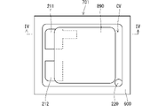
- FIG. 1 is a plan view schematically showing the configuration of a crystal oscillator according to Embodiment 1 of the present invention
- FIG. 2 is a schematic cross-sectional view along line II-II of FIG. 1
- FIG. FIG. 2 is a plan view schematically showing one step of a method for manufacturing the crystal oscillator of FIG. 1
- Figure 4 is a schematic cross-sectional view along line IV-IV of Figure 3
- 1 is a plan view schematically showing the configuration of a package according to Embodiment 1 of the present invention
- FIG. Figure 6 is a schematic cross-sectional view along line VI-VI of Figure 5
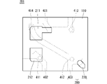
- FIG. 6 is a plan view omitting illustration of a metallized layer and a frame portion in FIG. 5 ;
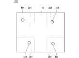
- FIG. 8 is a plan view schematically showing the substrate portion and via electrodes in FIG. 7, with package electrode pads indicated by dashed lines;
- FIG. 6 is a plan view omitting illustration of a metallized layer on the frame portion in FIG. 5 ;
- FIG. 10 is a schematic cross-sectional view along line XX of FIG. 9;
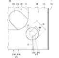
- FIG. 10 is a partially enlarged view of FIG. 9;
- FIG. 4 is a partial cross-sectional view schematically showing one step of the manufacturing method of the package according to Embodiment 1 of the present invention;
- FIG. 4 is a partial cross-sectional view schematically showing one step of the manufacturing method of the package according to Embodiment 1 of the present invention;
- FIG. 4 is a partial cross-sectional view schematically showing one step of the manufacturing method of the package according to Embodiment 1 of the present invention;
- FIG. 4 is a partial cross-sectional view schematically showing one step of the manufacturing method of the package according to Embodiment 1 of the present invention
- 11 is a diagram for explaining the details of the configuration of the via electrode shown in FIG. 10
- FIG. FIG. 16 is a diagram showing the configuration shown in FIG. 15 together with the metallized layer while considering the fine inclination of the upper surface of the frame of the frame.
- FIG. 10 is a diagram for explaining the details of the configuration of via electrodes included in the package according to the second embodiment of the present invention
- FIG. 18 is a view showing the configuration shown in FIG. 17 together with the metallization layer while considering the fine inclination of the top surface of the frame of the frame.
- FIG. 10 is a diagram for explaining the details of the configuration of via electrodes included in the package according to the third embodiment of the present invention
- FIG. 20 is a diagram showing the configuration shown in FIG. 19 together with the metallized layer while considering the fine inclination of the top surface of the frame of the frame.
- 16 is a micrograph showing an example corresponding to the configuration of FIG. 15
- 18 is a micrograph showing an example corresponding to the configuration of FIG. 17
- 20 is a micrograph showing an example corresponding to the configuration of FIG. 19;
- FIG. 1 is a plan view schematically showing the configuration of a crystal oscillator 900 (electrical component) according to the first embodiment.
- FIG. 2 is a schematic cross-sectional view along line II-II of FIG.
- FIG. 3 is a plan view schematically showing the configuration immediately after the crystal blank 890 (electrical element) is mounted in the manufacturing method of the crystal oscillator 900 (FIG. 1).
- FIG. 4 is a schematic cross-sectional view along line IV-IV of FIG.
- a crystal oscillator 900 has a package 701 , a crystal blank 890 , a brazing material 960 and a lid 980 .
- the package 701 is provided with a cavity CV.
- a crystal blank 890 is housed in the cavity CV and mounted on the device electrode pads 211 and 212 of the package 701 .
- Lid 980 is bonded to metallization layer 600 of package 701 by brazing material 960, thereby sealing cavity CV.
- Brazing material 960 is typically preferably made of an alloy containing gold, for example, an alloy containing gold and tin, in other words, an Au—Sn alloy.
- Lid 980 is made of metal, for example, an alloy containing iron and nickel. In this specification, an alloy is regarded as one type of metal.
- the metallized layer 600 is made of metal containing at least one of molybdenum and tungsten, for example.
- the surface of the metallized layer 600 (the surface facing the brazing material 960) may be provided with a plating layer, typically a gold plating layer. Also, a nickel plating layer may be provided as a base for the gold plating layer.
- the metallized layer 600 provided directly on the frame upper surface SF1 of the frame portion 120 of the package 701 and the lid 980 are joined only by the brazing material 960 .
- FIG. 5 is a plan view schematically showing the configuration of the package 701.
- FIG. FIG. 6 is a schematic cross-sectional view along line VI-VI of FIG.
- the package 701 has a ceramic portion 100, an element electrode pad 211, an element electrode pad 212, and package electrode pads 301-304. Although the details will be described later, the package 701 has a structure for electrical wiring provided in the ceramic part 100 .
- the ceramic part 100 is made of ceramic, preferably containing oxide as a main component, more preferably containing alumina as a main component, for example substantially made of alumina.
- Ceramic portion 100 includes a substrate portion 110 and a frame portion 120 .
- the material of the substrate portion 110 and the material of the frame portion 120 may be the same.
- the frame portion 120 is laminated on the substrate portion 110 in the thickness direction (vertical direction in FIG. 6).
- the frame portion 120 has a frame upper surface SF1 (first surface) and a frame lower surface SF2 (second surface opposite to the first surface in the thickness direction).
- the frame portion 120 also has an inner wall surface that connects the upper frame surface SF1 and the lower frame surface SF2, and the inner wall surface is the side wall of the cavity CV.
- the substrate portion 110 has a substrate upper surface SF3 (third surface).
- the substrate top surface SF3 has a support surface portion SF3S that supports the frame bottom surface SF2 of the frame portion 120, and a cavity surface portion SF3C that faces the cavity CV.
- Cavity surface portion SF3C forms the bottom surface of cavity CV.
- the element electrode pads 211 and 212 are arranged on the ceramic part 100 (FIG. 6) facing the cavity CV. Specifically, the element electrode pads 211 and the element electrode pads 212 are arranged on the upper surface (the surface facing the cavity CV) of the substrate section 110 (FIG. 6).
- Package electrode pads 301-304 are arranged on the ceramic part 100 (FIG. 6) outside the cavity CV. Specifically, the package electrode pads 301 to 304 are arranged on the bottom surface (the surface opposite to the surface facing the cavity CV) of the substrate section 110 (FIG. 6).
- the relay electrode 220 (FIG. 5) is provided on the substrate upper surface SF3 of the substrate portion 110 (FIG. 6).
- the relay electrode 220 is arranged at least partially on the support surface portion SF3S (FIG. 6). Therefore, the relay electrode 220 ( FIG. 5 ) is at least partially covered by the frame 120 .
- the relay electrode 220 may further have a portion that is not covered by the frame portion 120 and is arranged on the bottom surface of the cavity CV. In other words, the relay electrode 220 may be only partially covered by the frame portion 120 .
- FIG. 7 is a plan view omitting illustration of the metallized layer 600 (FIG. 5) and the frame portion 120 (FIG. 6).
- 8 is a plan view schematically showing the substrate portion 110 and the substrate via electrodes 411 to 414 in FIG. 7, with the package electrode pads 301 to 304 indicated by broken lines.
- Wiring layers 401 to 403 are embedded in the vicinity of the upper surface of the substrate portion 110 of the ceramic portion 100 .
- the wiring layer 401 is in contact with the element electrode pad 211
- the wiring layer 402 is in contact with the element electrode pad 212
- the wiring layer 403 is in contact with the relay electrode 220 .
- the wiring layers 401 to 403 may be covered with an insulating film 110i (see FIG. 10) as part of the substrate section 110 to the extent that these contacts are not hindered. are insulated by the insulating film 110i.
- the electrode layer 200 is configured by the wiring layer 403 and the relay electrode 220 .
- the package 701 has substrate via electrodes 411 to 414 embedded in the substrate portion 110 of the ceramic portion 100 .
- a substrate via electrode 411 connects the wiring layer 402 and the package electrode pad 301 to each other.
- a substrate via electrode 412 connects the wiring layer 403 and the package electrode pad 302 to each other.
- a substrate via electrode 413 connects the wiring layer 401 and the package electrode pad 303 to each other.
- a substrate via electrode 414 connects the wiring layer 403 and the package electrode pad 304 to each other.
- the element electrode pad 211 is electrically connected to the package electrode pad 303
- the element electrode pad 212 is electrically connected to the package electrode pad 301
- the relay electrode 220 is connected to the package electrode pad 302 and It is electrically connected to the package electrode pad 304 .
- FIG. 9 is a plan view in which illustration of the metallized layer 600 in FIG. 5 is omitted. 10 is a schematic cross-sectional view along line XX of FIG. 9. FIG. 11 is a partially enlarged view of FIG. 9. FIG.
- a frame lower surface SF2 of the frame portion 120 has an inner edge EI surrounding the cavity CV and an outer edge EO surrounding the inner edge EI.
- a minimum dimension WD (FIG. 11) between the inner edge EI and the outer edge EO may be 200 ⁇ m or less, typically 20 ⁇ m or more and 110 ⁇ m or less.
- the frame portion 120 has an outer wall surface SF4 that connects the upper frame surface SF1 and the outer edge EO of the lower frame surface SF2.
- the frame portion 120 has an inner wall surface that connects the upper frame surface SF1 and the inner edge EI of the lower frame surface SF2, and the inner wall surface faces the cavity CV.
- the outer wall surface SF4 has a fired surface SF4A connected to the frame upper surface SF1 and a fracture surface SF4B connected to the frame lower surface SF2.
- the fracture surface SF4B may be a plane approximately perpendicular to the top surface SF1 of the frame.
- the firing surface SF4A may be a bevel surface chamfering between the frame top surface SF1 and the fracture surface SF4B, as shown in FIG.
- the normal direction of the firing surface SF4A may be different from the normal direction of the frame upper surface SF1 and the fracture surface SF4B, and may be between them.
- the wiring layer 403 and the relay electrode 220 constitute the electrode layer 200 on the substrate upper surface SF3 of the substrate portion 110.
- the substrate section 110 has the insulating film 110i (FIG. 10) as a part thereof.
- the insulating film 110i may be omitted depending on the package design.
- the electrode layer 200 may be composed of only one of the wiring layer 403 and the relay electrode 220 .
- the electrode layer 200 may have the wiring layer 403 while omitting the relay electrode 220. In this case, the boundary position between the wiring layer 403 and the insulating film 110i (right end position of the wiring layer 403 in FIG.
- the relay electrode 220 may be shifted to the end position of the relay electrode 220 on the support surface portion SF3S (the right end position of the relay electrode 220 in FIG. 10), and the relay electrode 220 may be omitted.
- the edge of the insulating film 110i facing the cavity CV may be deformed to reach the frame 120, in which case the electrode layer 200 may be separated from the cavity CV by the insulating film 110i.
- electrode layer 200 typically spans support surface portion SF3S and cavity surface portion SF3C as shown in FIG. you can In addition, the electrode layer 200 has an end (the right end in FIG. 10) away from the outer edge EO of the frame lower surface SF2 of the frame portion 120 in the present embodiment, but this end is deformed to reach the outer edge EO. you can
- the package 701 has via electrodes 510 .
- the via electrode 510 penetrates the frame portion 120 between the frame top surface SF1 and the frame bottom surface SF2.
- the via electrode 510 has an end surface SFA on the frame top surface SF1 and a bottom surface SFB on the frame bottom surface SF2.
- the center position of the end surface SFA and the center position of the bottom surface SFB may be approximately the same.
- the bottom surface SFB is in contact with the electrode layer 200, and is in contact with the relay electrode 220 in this embodiment.
- the relay electrode 220 is in contact with the wiring layer 403, and the substrate via electrode 412 and the substrate via electrode 414 are connected to the wiring layer 403 (FIG. 7).
- substrate via electrode 412 and substrate via electrode 414 are electrically connected to via electrode 510 . Furthermore, the end surface SFA of the via electrode 510 is in contact with the metallization layer 600 (FIG. 6). Thus, the metallization layer 600 is electrically connected to the package electrode pads 302 and 304 via the substrate via electrodes 412 and 414, respectively (see FIG. 8).
- the end surface SFA of the via electrode 510 has a diameter DA (FIG. 11).
- the diameter DA is smaller than the smallest dimension WD and may be 50 ⁇ m or less.
- Bottom surface SFB of via electrode 510 has diameter DB (FIG. 11) smaller than diameter DA.
- the via electrode 510 has a diameter of (DA+DB)/2 or less at an intermediate position between the end surface SFA and the bottom surface SFB (the average position between the end surface SFA and the bottom surface SFB) in the thickness direction (vertical direction in FIG. 10). It is preferable to have
- the taper ratio (percentage of diameter DB to diameter DA) is preferably less than 60%.
- the bottom surface SFB has a minimum dimension LI from the inner edge EI of the frame bottom surface SF2 of the frame portion 120 and a minimum dimension LO from the outer edge EO of the frame bottom surface SF2 of the frame portion 120.
- LO>LI is satisfied, preferably LO ⁇ LI ⁇ 1.5.
- the shapes of the end face SFA and the bottom face SFB are approximately circular, but these shapes may differ slightly from geometrically strict circular shapes due to manufacturing errors. good.
- the diameters DA and DB may be calculated by approximating the end face SFA and the bottom face SFB with circular shapes.
- the inner edge EI of the frame lower surface SF2 (see FIG. 10) has a first linear portion (vertical linear portion in the figure) and a direction perpendicular to the first linear portion. It has a second straight portion extending (horizontal straight portion in the drawing) and a corner portion connecting them to each other.
- Minimum dimension LI may be the dimension to this corner.
- FIGS. 12 and 13 are partial cross-sectional views schematically showing one step of a manufacturing method for collectively manufacturing a plurality of packages 701.
- FIG. 12 to 14 for convenience of explanation, the illustration of the portion to be the metallized layer 600 (FIG. 6) is omitted. Since the metallized layer 600 can be formed by a well-known technique, for example, by applying a conductive paste and baking it, the explanation thereof is omitted. Note that the firing may be performed in common with the firing step described later.
- 12 and 13 show the state before the firing process for changing the state of FIG. 13 to the state of FIG.
- each structure in FIGS. 12 and 13 is made of unfired material, unlike the finished package 701, but for the sake of explanation, this difference in materials is ignored and the reference numerals representing the structure of package 701 are used. 12 and 13 also have the same reference numerals.
- a green sheet 700G (FIG. 12) includes a plurality of regions 701G, each of which eventually becomes a package 701.
- via electrodes 510 correspond to through holes filled with conductive paste.
- the through holes are formed by laser processing the green sheet 700G.
- a trench TR1 (FIG. 13) is formed in the frame upper surface SF1 of the green sheet 700G. Further, a trench TR2 (FIG. 13) is formed on the surface of the green sheet 700G opposite to the frame upper surface SF1. Trench TR1 and trench TR2 are arranged to face each other in the thickness direction. Trench TR1 and trench TR2 are formed, for example, by pressing a cutting edge against green sheet 700G. After that, a firing process for firing the green sheet 700G (FIG. 13) is performed. In addition, after the firing process, a plating process may be performed as necessary.
- a fired sheet 700F (FIG. 14) is formed by the firing process described above.
- the inner surface of trench TR1 is exposed to a firing atmosphere. Therefore, the inner surface of the trench TR1 of the firing sheet 700F becomes the firing surface.
- the fired surface becomes the fired surface SF4A of the package 701 (FIG. 10).
- a breaking step is performed in which cracks are generated from trenches TR1.
- a broken surface is formed by breaking the frame portion 120 by the breaking process.
- the fracture surface becomes the fracture surface SF4B (FIG. 10) of the package 701.
- the breaking step may be a step of generating a crack between trench TR1 and trench TR2.
- a plurality of packages 701 are cut out from the fired sheet 700F by the breaking process.
- the crack from the trench TR1 ideally extends along the thickness direction as indicated by the solid-line arrow in the drawing, but in practice, as indicated by the broken-line arrow in the drawing, the crack extends along the thickness direction.
- one via electrode 510 left via electrode 510 in the drawing
- the minimum dimension LO (FIG. 11) of the frame bottom surface SF2 of the frame portion 120 may become small. Since an excessively small minimum dimension LO is likely to lead to leaks in the package 701, it is desired that the minimum dimension LO has some margin. According to the present embodiment, it becomes easier to ensure this margin.
- FIG. 15 is a diagram for explaining the details of the configuration of via electrode 510 (FIG. 10).
- Via electrode 510 has a portion extending in a tapered shape from end surface SFA to bottom surface SFB over the entire thickness direction (vertical direction in the drawing). This tapered shape preferably has a taper angle TP AV of 5 degrees or more with respect to the thickness direction LD.
- Via electrode 520 has a side surface connecting end surface SFA and bottom surface SFB.
- a point KA and a point KB respectively indicate the positions of the side surfaces at the positions of the end surface SFA and the bottom surface SFB in the thickness direction.
- a point KV indicates the position of the side surface between the points KA and KB in the thickness direction.
- Point KW indicates the position of the side surface between point KV and point KB in the thickness direction.
- points KV and KW are substantially positioned on a straight line connecting points KA and KB.
- FIG. 16 is a diagram showing the configuration shown in FIG. 15 together with the metallized layer 600 (see FIG. 6) while taking into consideration the fine inclination of the frame upper surface SF1, which was omitted in FIG.
- the frame upper surface SF1 of the frame portion 120 includes an inclined area SF1d (first area) directly connected to the end surface SFA of the via electrode 510 and a parallel area SF1f (second area) connected to the end surface SFA of the via electrode 510 via the inclined area SF1d. area) and
- the parallel region SF1f is perpendicular to the thickness direction. Inclined region SF1d is inclined with respect to parallel region SF1f so that the thickness of frame portion 120 decreases as it approaches end surface SFA of via electrode 510 .
- the angle of this inclination is, for example, 4° or more and 20° or less.
- the sloped region SF1d may surround the end surface SFA of the via electrode 510, and the parallel region SF1f may surround the sloped region SF1d.
- the metallized layer 600 is provided on the inclined area SF1d and the parallel area SF1f of the frame top surface SF1 and is in contact with the end surface SFA of the via electrode 510 .
- the diameter DB of the bottom surface SFB is smaller than the diameter DA of the end surface SFA.
- the interface between frame bottom surface SF2 (FIG. 10) of frame portion 120 and substrate top surface SF3 (FIG. 10) of substrate portion 110 is widened.
- the lamination interface between the ceramics is widened around the bottom surface SFB of the via electrode 510 .
- the bottom surface SFB of the via electrode 510 is arranged so as to satisfy LO>LI, the bottom surface SFB and the outer edge EO of the frame bottom surface SF2 of the frame portion 120 In between, a large area is secured where the lamination interface between the ceramics is arranged.
- the lamination interface between ceramics has higher airtightness than the lamination interface between metal and ceramics. Therefore, it is possible to suppress deterioration in airtightness due to leakage along the lamination interface.
- the diameter DA of the via electrode 510 may be 50 ⁇ m or less.
- the minimum dimension WD (FIG. 11) of the frame portion 120 can also be miniaturized. Leakage along the lamination interface between the substrate portion 110 and the frame portion 120 tends to become a problem as the miniaturization progresses, but this problem is effectively suppressed for the reasons described above.
- the minimum dimension between the inner edge EI and the outer edge EO of the frame lower surface SF2 of the frame portion 120 may be 200 ⁇ m or less. Leakage along the lamination interface between the substrate portion 110 and the frame portion 120 tends to become a problem as miniaturization advances, but this problem is effectively suppressed for the reasons described above.
- the via electrode 510 may have a diameter of (DA+DB)/2 or less at an intermediate position between the end surface SFA and the bottom surface SFB in the thickness direction (vertical direction in FIG. 10), referring to FIG. Thereby, a sufficient distance can be secured between the intermediate position of the via electrode 510 and the outer wall surface SF4 of the frame portion 120 . Therefore, the airtightness reliability between the via electrode 510 and the frame portion 120 can be enhanced.
- the via electrode 510 has a tapered portion extending from the end face SFA in the thickness direction (vertical direction in FIG. 10). This makes it easier to secure a distance between the via electrode 510 and the outer wall surface SF4 of the frame portion 120 immediately below the end surface SFA. Therefore, the airtightness reliability between the via electrode 510 and the frame portion 120 can be enhanced. Especially in the present embodiment, since the entire via electrode 510 extends in a tapered shape, this effect can be obtained more sufficiently.
- the taper angle TP AV (FIG. 15) may be 5 degrees or greater. This makes it easier to sufficiently secure the distance between the via electrode 510 and the outer wall surface SF4 (FIG. 10) of the frame portion 120 immediately below the end surface SFA.
- the outer wall surface SF4 (FIG. 10) of the frame portion 120 has a fired surface SF4A connected to the frame upper surface SF1 and a fracture surface SF4B connected to the frame lower surface SF2. Since the fractured surface SF4B is formed by the breaking process, the minimum dimension LO (FIG. 11) may become smaller due to the influence of variations in the process. However, since DA>DB and LO>LI are satisfied as described above, the minimum dimension LO is unlikely to be too small. Therefore, it is possible to prevent insufficient airtightness of the frame portion 120 due to an excessively small minimum dimension LO.
- the inclined region SF1d (FIG. 16) is inclined as described above, the side surface of the via electrode 510 (FIG. 15) and the frame upper surface SF1 are formed while maintaining the diameter DA and the diameter DB of the via electrode 510 (FIG. 15).
- the obtuse angle SH can be made larger. Therefore, the thermal stress caused by the difference in thermal expansion between the via electrode 510 and the metallized layer 600 mainly made of metal and the frame portion 120 made of ceramics can be relaxed. Therefore, cracks or peeling between the via electrode 510 and the frame portion 120 due to thermal stress can be prevented.
- the obtuse angle SH increases as the diameter DA (Fig. 15) increases.
- the diameter DA has a design upper limit.
- the obtuse angle SH increases as the diameter DB (FIG. 15) decreases.
- the smaller the diameter DB the smaller the area of the bottom surface SFB of the via electrode 510. Therefore, in the configuration of FIG. easy enough.
- the slope region SF1d may be omitted when the above effect of the slope region SF1d is not particularly required.
- the region of frame top surface SF1 directly connected to end surface SFA of via electrode 510 may be perpendicular to the thickness direction.
- FIG. 17 is a diagram for explaining the details of the configuration of via electrodes 520 included in package 702 according to the second embodiment.
- the side surface of the via electrode 520 has at least one bending point in a cross-sectional view (FIG. 17) parallel to the thickness direction. have KW.
- Via electrode 520 has a portion 521 having a side surface from point KA to point KV, a portion 522 having a side surface from point KV to point KW, and a portion 523 having a side surface from point KW to point KB.
- the portion 521 extends in a tapered shape from the end surface SFA in the thickness direction, and the taper angle TP AV of this tapered shape is preferably 5 degrees or more.
- Portion 521 preferably has a thickness equal to or greater than half the thickness of frame portion 120 .
- the portion 522 has a gently tapered shape or a cylindrical shape compared to the portion 521 .
- Portion 523 has a sharper taper than portion 522 .
- FIG. 18 is a diagram showing the configuration shown in FIG. 17 together with the metallized layer 600 (see FIG. 6) while taking into consideration the fine inclination of the frame upper surface SF1, which was omitted in FIG.
- the configuration shown in FIG. 18 corresponds to the configuration shown in FIG. 16 in which via electrode 510 (embodiment 1) is replaced with via electrode 520 (present embodiment 2).
- the configuration shown in FIG. 18 also provides the same effects as those described in the first embodiment in relation to the configuration shown in FIG.
- a portion 521 of the via electrode 520 has a thickness of 1/2 or more of the thickness of the frame portion 120 . Thereby, the distance between the via electrode 520 and the outer wall surface SF4 (see FIG. 10) of the frame portion 120 can be sufficiently increased by the tapered shape.
- the side surface of the via electrode 520 has bending points (specifically, points KV and KW). As a result, peeling between the side surface of the via electrode 520 and the frame portion 120 due to sintering shrinkage during manufacture of the package 702 can be suppressed. This effect is enhanced by the fact that points KV and KW as inflection points are curved in opposite directions.
- FIG. 19 is a diagram for explaining the details of the configuration of via electrodes 530 included in package 703 according to the third embodiment.
- Via electrode 530 has a portion 531 having a side surface from point KA to point KV, a portion 532 having a side surface from point KV to point KW, and a portion 533 having a side surface from point KW to point KB.
- the portion 531 extends in a tapered shape from the end surface SFA in the thickness direction, and the taper angle TP AV of this tapered shape is preferably 5 degrees or more.
- Portion 531 preferably has a thickness equal to or greater than half the thickness of frame portion 120 .
- Portion 532 has a reverse tapered shape in the direction from end surface SFA to bottom surface SFB.
- Portion 533 has a tapered shape in the direction from end surface SFA to bottom surface SFB.
- FIG. 20 is a diagram showing the configuration shown in FIG. 19 together with the metallized layer 600 (see FIG. 6) while taking into consideration the fine inclination of the frame upper surface SF1, which was omitted in FIG.
- the configuration shown in FIG. 20 corresponds to the configuration shown in FIG. 16 in which via electrode 510 (first embodiment) is replaced with via electrode 530 (third embodiment).
- the configuration shown in FIG. 20 also provides the same effects as those described in the first embodiment in relation to the configuration shown in FIG.
- the configuration other than the above is substantially the same as the configuration of the second embodiment described above, the same or corresponding elements are denoted by the same reference numerals, and the description thereof will not be repeated. According to the present embodiment, the effect of suppressing separation between the side surface of via electrode 520 and frame portion 120 due to sintering shrinkage is further enhanced as compared with the second embodiment.
- green sheet 700G (FIG. 12) through holes to be filled with via electrodes 510 are formed by laser processing as described above.
- the packages of Examples 1 to 8 were produced by setting the irradiation time and number of times of laser light irradiation in the processing as shown in Table 1 below.
- the green sheet 700G was irradiated with laser light having a wavelength of 9.4 ⁇ m and an average output of 200 W from a CO 2 laser through a mask having an opening diameter of 0.8 mm.
- the point KV (FIG. 15) is the intermediate position (in other words, average position) between the points KA and KB in the thickness direction
- the point KW (FIG. 15) is the intermediate position between the points KV and KB in the thickness direction.
- positions in other words mean positions
- the diameter DA was 46 ⁇ m
- the diameter DV (diameter through point KV) was 34 ⁇ m
- the diameter DW (diameter through point KW) was 28 ⁇ m
- the diameter DB was 23 ⁇ m. rice field.
- the taper angle from point KA to point KB is 5.9 degrees
- the taper angle from point KA to point KV is 6.1 degrees
- the taper angle from point KV to point KW is 5.7 degrees
- the taper angle from point KW to point KB was 5.9 degrees.
- the entire via electrode had a substantially monotonic tapered shape within the range of 5.9 ⁇ 0.2 degrees.
- FIG. 21 shows an example of a microscope photograph during this observation.
- the metallized layer 600 (see FIG. 6) is locally thickened at the connection portion with the end face SFA (see FIG. 15) of the via electrode 510.
- the diameter DA (see FIG. 15) was measured at the connecting portion (arrow portion in FIG. 21).
- FIGS. 22 and 23 which will be described later.
- the example of FIG. 21 corresponds to the configuration of FIG. 16, and the metallized layer 600 protrudes downward from the dashed line portion (FIG. 16), so that it is locally thickened at the connection portion of the via electrode 510 with the end face SFA.
- the obtuse angle SH (FIG. 16) was 113° on each of the left and right sides of via electrode 510 .
- Example 6 a shape corresponding to the via electrode 520 (FIG. 17) was obtained. Specifically, inflection points such as point KV (FIG. 17) and point KW (FIG. 17) were observed. In this observation, the point KV (FIG. 17) is roughly the middle position (in other words, the average position) between the points KA and KB in the thickness direction, and the point KW (FIG. 17) is the point KV and the point KB in the thickness direction. It was roughly in the middle position (in other words, the average position).
- the diameter DA was 47 ⁇ m
- the diameter DV (diameter through point KV) was 34 ⁇ m
- the diameter DW (diameter through point KW) was 33 ⁇ m
- the diameter DB was 23 ⁇ m.
- the taper angle from point KA to point KB is 6.1 degrees
- the taper angle from point KA to point KV is 6.5 degrees
- the taper angle from point KV to point KW is 0.8 degrees.
- the taper angle from point KW to point KB was 10.5 degrees.
- FIG. 22 shows an example of a microscope photograph during this observation.
- the example of FIG. 22 corresponds to the configuration of FIG. 18, and the metallized layer 600 protrudes downward from the dashed line portion (FIG. 18) and is locally thickened at the connection portion of the via electrode 520 with the end surface SFA.
- the obtuse angle SH (FIG. 18) was 114° on each of the left and right sides of via electrode 520 .
- a shape corresponding to the via electrode 530 (FIG. 19) was obtained. Specifically, inflection points such as point KV (FIG. 19) and point KW (FIG. 19) were observed. In this observation, the point KV (FIG. 19) is roughly the middle position (in other words, the average position) between the points KA and KB in the thickness direction, and the point KW (FIG. 19) is the point KV and the point KB in the thickness direction. It was roughly in the middle position (in other words, the average position).
- the diameter DA was 45 ⁇ m
- the diameter DV (diameter through point KV) was 31 ⁇ m
- the diameter DW (diameter through point KW) was 32 ⁇ m
- the diameter DB was 18 ⁇ m.
- the taper angle from point KA to point KB is 6.9 degrees
- the taper angle from point KA to point KV is 6.9 degrees
- the taper angle from point KV to point KW is -0.8 degrees. degrees and the taper angle from point KW to point KB was 14.4 degrees.
- the taper angle from point KV to point KW has a negative value, which means an inverse taper shape.
- FIG. 23 shows an example of a microscope photograph during this observation. The example of FIG. 23 corresponds to the configuration of FIG.
- obtuse angles SH were 102° and 120° on the left and right sides of via electrode 530 (FIG. 20), respectively.
- Embodiments 1 to 3 of the present invention and their modifications have been described above. These embodiments and modifications may be freely combined with each other as long as they do not contradict each other.
Landscapes
- Piezo-Electric Or Mechanical Vibrators, Or Delay Or Filter Circuits (AREA)
- Control And Other Processes For Unpacking Of Materials (AREA)
Priority Applications (5)
| Application Number | Priority Date | Filing Date | Title |
|---|---|---|---|
| JP2023505749A JP7244712B2 (ja) | 2021-03-19 | 2022-01-21 | パッケージ |
| CN202280006442.XA CN116250078B (zh) | 2021-03-19 | 2022-01-21 | 封装体 |
| TW111107455A TWI799161B (zh) | 2021-03-19 | 2022-03-02 | 封裝體 |
| TW112107958A TWI894536B (zh) | 2021-03-19 | 2022-03-02 | 封裝體 |
| JP2023036199A JP2023060888A (ja) | 2021-03-19 | 2023-03-09 | パッケージ |
Applications Claiming Priority (2)
| Application Number | Priority Date | Filing Date | Title |
|---|---|---|---|
| JP2021045808 | 2021-03-19 | ||
| JP2021-045808 | 2021-03-19 |
Publications (1)
| Publication Number | Publication Date |
|---|---|
| WO2022196097A1 true WO2022196097A1 (ja) | 2022-09-22 |
Family
ID=83320238
Family Applications (1)
| Application Number | Title | Priority Date | Filing Date |
|---|---|---|---|
| PCT/JP2022/002211 Ceased WO2022196097A1 (ja) | 2021-03-19 | 2022-01-21 | パッケージ |
Country Status (4)
| Country | Link |
|---|---|
| JP (2) | JP7244712B2 (https=) |
| CN (1) | CN116250078B (https=) |
| TW (2) | TWI799161B (https=) |
| WO (1) | WO2022196097A1 (https=) |
Families Citing this family (1)
| Publication number | Priority date | Publication date | Assignee | Title |
|---|---|---|---|---|
| TWI863479B (zh) * | 2022-08-09 | 2024-11-21 | 日商Ngk電子器件股份有限公司 | 封裝體 |
Citations (5)
| Publication number | Priority date | Publication date | Assignee | Title |
|---|---|---|---|---|
| JP2002064354A (ja) * | 2000-08-18 | 2002-02-28 | Daishinku Corp | 表面実装型圧電振動子用パッケージおよび表面実装型圧電振動子用パッケージの製造方法 |
| JP2003218660A (ja) * | 2002-01-24 | 2003-07-31 | Kyocera Corp | 圧電振動子収納用パッケージ |
| JP2013004693A (ja) * | 2011-06-15 | 2013-01-07 | Daishinku Corp | 電子部品用パッケージおよび圧電振動デバイス |
| JP2019192825A (ja) * | 2018-04-26 | 2019-10-31 | 京セラ株式会社 | 電子部品収納用パッケージ、電子装置、および電子モジュール |
| WO2020208999A1 (ja) * | 2019-04-12 | 2020-10-15 | Ngkエレクトロデバイス株式会社 | 電子部品収納用パッケージ |
Family Cites Families (17)
| Publication number | Priority date | Publication date | Assignee | Title |
|---|---|---|---|---|
| JP2920854B2 (ja) * | 1991-08-01 | 1999-07-19 | 富士通株式会社 | ビィアホール構造及びその形成方法 |
| JP3426741B2 (ja) * | 1994-10-27 | 2003-07-14 | 京セラ株式会社 | 半導体素子収納用パッケージ |
| JP2003110037A (ja) * | 2001-09-27 | 2003-04-11 | Kyocera Corp | 電子部品収納用パッケージ |
| US20040021219A1 (en) * | 2002-08-01 | 2004-02-05 | James Studebaker | Method of mounting integrated circuit die in a package using a solder preform having isolatable portions |
| JP4167614B2 (ja) * | 2003-09-24 | 2008-10-15 | 株式会社住友金属エレクトロデバイス | 電子部品収納用パッケージ |
| US7075775B2 (en) * | 2004-05-27 | 2006-07-11 | Kyocera Corporation | Chip-type electronic component |
| JP4546990B2 (ja) * | 2007-06-21 | 2010-09-22 | 日本特殊陶業株式会社 | セラミックパッケージ及びその製造方法 |
| DE102008007001B4 (de) * | 2008-01-31 | 2016-09-22 | Globalfoundries Dresden Module One Limited Liability Company & Co. Kg | Vergrößern des Widerstandsverhaltens gegenüber Elektromigration in einer Verbindungsstruktur eines Halbleiterbauelements durch Bilden einer Legierung |
| US20100013060A1 (en) * | 2008-06-22 | 2010-01-21 | Taiwan Semiconductor Manufacturing Company, Ltd. | Method of forming a conductive trench in a silicon wafer and silicon wafer comprising such trench |
| JP5442974B2 (ja) * | 2008-09-16 | 2014-03-19 | 日本特殊陶業株式会社 | セラミック部品の製造方法 |
| JP5987347B2 (ja) * | 2012-02-24 | 2016-09-07 | セイコーエプソン株式会社 | 電子デバイスの製造方法 |
| WO2014115766A1 (ja) * | 2013-01-22 | 2014-07-31 | 京セラ株式会社 | 電子素子搭載用パッケージ、電子装置および撮像モジュール |
| JP6336829B2 (ja) * | 2014-06-19 | 2018-06-06 | 京セラ株式会社 | 配線基板、パッケージおよび電子機器 |
| US9711452B2 (en) * | 2014-12-05 | 2017-07-18 | International Business Machines Corporation | Optimized wires for resistance or electromigration |
| CN108461450B (zh) * | 2015-11-25 | 2021-06-18 | 京瓷株式会社 | 电子部件收纳用封装体、电子装置以及电子模块 |
| JP6834841B2 (ja) * | 2017-08-09 | 2021-02-24 | 三菱電機株式会社 | 半導体装置 |
| JP7102256B2 (ja) * | 2018-06-27 | 2022-07-19 | 株式会社村田製作所 | 積層セラミック電子部品 |
-
2022
- 2022-01-21 WO PCT/JP2022/002211 patent/WO2022196097A1/ja not_active Ceased
- 2022-01-21 CN CN202280006442.XA patent/CN116250078B/zh active Active
- 2022-01-21 JP JP2023505749A patent/JP7244712B2/ja active Active
- 2022-03-02 TW TW111107455A patent/TWI799161B/zh active
- 2022-03-02 TW TW112107958A patent/TWI894536B/zh active
-
2023
- 2023-03-09 JP JP2023036199A patent/JP2023060888A/ja active Pending
Patent Citations (5)
| Publication number | Priority date | Publication date | Assignee | Title |
|---|---|---|---|---|
| JP2002064354A (ja) * | 2000-08-18 | 2002-02-28 | Daishinku Corp | 表面実装型圧電振動子用パッケージおよび表面実装型圧電振動子用パッケージの製造方法 |
| JP2003218660A (ja) * | 2002-01-24 | 2003-07-31 | Kyocera Corp | 圧電振動子収納用パッケージ |
| JP2013004693A (ja) * | 2011-06-15 | 2013-01-07 | Daishinku Corp | 電子部品用パッケージおよび圧電振動デバイス |
| JP2019192825A (ja) * | 2018-04-26 | 2019-10-31 | 京セラ株式会社 | 電子部品収納用パッケージ、電子装置、および電子モジュール |
| WO2020208999A1 (ja) * | 2019-04-12 | 2020-10-15 | Ngkエレクトロデバイス株式会社 | 電子部品収納用パッケージ |
Also Published As
| Publication number | Publication date |
|---|---|
| JP7244712B2 (ja) | 2023-03-22 |
| TWI894536B (zh) | 2025-08-21 |
| JP2023060888A (ja) | 2023-04-28 |
| TW202240797A (zh) | 2022-10-16 |
| TWI799161B (zh) | 2023-04-11 |
| CN116250078A (zh) | 2023-06-09 |
| JPWO2022196097A1 (https=) | 2022-09-22 |
| TW202329339A (zh) | 2023-07-16 |
| CN116250078B (zh) | 2023-10-24 |
Similar Documents
| Publication | Publication Date | Title |
|---|---|---|
| CN103959461B (zh) | 陶瓷封装 | |
| JP5278044B2 (ja) | パッケージ部材および該パッケージ部材の製造方法および該パッケージ部材を用いた圧電振動デバイス | |
| JP5312223B2 (ja) | 配線基板 | |
| JP7244712B2 (ja) | パッケージ | |
| JP7650780B2 (ja) | パッケージおよびその製造方法 | |
| JP7430579B2 (ja) | パッケージおよびその製造方法 | |
| WO2018180861A1 (ja) | 音叉型圧電振動片および当該音叉型圧電振動片を用いた音叉型圧電振動子 | |
| JP7562767B2 (ja) | パッケージ | |
| TWI863479B (zh) | 封裝體 | |
| JP2014172100A (ja) | 押圧溝形成用スリット刃及びセラミックパッケージの製造方法 | |
| TW202610010A (zh) | 構造體、安裝用構造及封裝體 | |
| JP5725898B2 (ja) | 電子部品収納用パッケージ | |
| JP7518951B2 (ja) | パッケージ | |
| TWI858846B (zh) | 封裝體 | |
| CN117595821A (zh) | 封装体 | |
| CN117595822A (zh) | 封装体 | |
| TW202240795A (zh) | 封裝體及其製造方法 | |
| JP7788889B2 (ja) | パッケージ | |
| JP2001144201A (ja) | 電子部品装置 | |
| JP7683051B2 (ja) | パッケージの製造方法 | |
| JP3783605B2 (ja) | 気密封止パッケージおよびこれを用いたデバイス | |
| JP6334192B2 (ja) | 圧電デバイスおよびその実装構造 | |
| JP2010182709A (ja) | 電子部品パッケージ、電子部品パッケージの製造方法、及び圧電デバイス | |
| JP6629660B2 (ja) | セラミックパッケージおよびその製造方法 | |
| JP2005268350A (ja) | 電子部品収納用パッケージ |
Legal Events
| Date | Code | Title | Description |
|---|---|---|---|
| 121 | Ep: the epo has been informed by wipo that ep was designated in this application |
Ref document number: 22770859 Country of ref document: EP Kind code of ref document: A1 |
|
| ENP | Entry into the national phase |
Ref document number: 2023505749 Country of ref document: JP Kind code of ref document: A |
|
| NENP | Non-entry into the national phase |
Ref country code: DE |
|
| 122 | Ep: pct application non-entry in european phase |
Ref document number: 22770859 Country of ref document: EP Kind code of ref document: A1 |