WO2022196019A1 - ガラス基板、貫通孔形成用ガラス原板及びガラス基板の製造方法 - Google Patents
ガラス基板、貫通孔形成用ガラス原板及びガラス基板の製造方法 Download PDFInfo
- Publication number
- WO2022196019A1 WO2022196019A1 PCT/JP2021/047908 JP2021047908W WO2022196019A1 WO 2022196019 A1 WO2022196019 A1 WO 2022196019A1 JP 2021047908 W JP2021047908 W JP 2021047908W WO 2022196019 A1 WO2022196019 A1 WO 2022196019A1
- Authority
- WO
- WIPO (PCT)
- Prior art keywords
- glass substrate
- holes
- glass
- less
- era
- Prior art date
- Legal status (The legal status is an assumption and is not a legal conclusion. Google has not performed a legal analysis and makes no representation as to the accuracy of the status listed.)
- Ceased
Links
Images




Classifications
-
- C—CHEMISTRY; METALLURGY
- C03—GLASS; MINERAL OR SLAG WOOL
- C03C—CHEMICAL COMPOSITION OF GLASSES, GLAZES OR VITREOUS ENAMELS; SURFACE TREATMENT OF GLASS; SURFACE TREATMENT OF FIBRES OR FILAMENTS MADE FROM GLASS, MINERALS OR SLAGS; JOINING GLASS TO GLASS OR OTHER MATERIALS
- C03C15/00—Surface treatment of glass, not in the form of fibres or filaments, by etching
-
- C—CHEMISTRY; METALLURGY
- C03—GLASS; MINERAL OR SLAG WOOL
- C03C—CHEMICAL COMPOSITION OF GLASSES, GLAZES OR VITREOUS ENAMELS; SURFACE TREATMENT OF GLASS; SURFACE TREATMENT OF FIBRES OR FILAMENTS MADE FROM GLASS, MINERALS OR SLAGS; JOINING GLASS TO GLASS OR OTHER MATERIALS
- C03C23/00—Other surface treatment of glass not in the form of fibres or filaments
-
- C—CHEMISTRY; METALLURGY
- C03—GLASS; MINERAL OR SLAG WOOL
- C03C—CHEMICAL COMPOSITION OF GLASSES, GLAZES OR VITREOUS ENAMELS; SURFACE TREATMENT OF GLASS; SURFACE TREATMENT OF FIBRES OR FILAMENTS MADE FROM GLASS, MINERALS OR SLAGS; JOINING GLASS TO GLASS OR OTHER MATERIALS
- C03C23/00—Other surface treatment of glass not in the form of fibres or filaments
- C03C23/007—Other surface treatment of glass not in the form of fibres or filaments by thermal treatment
-
- G—PHYSICS
- G09—EDUCATION; CRYPTOGRAPHY; DISPLAY; ADVERTISING; SEALS
- G09F—DISPLAYING; ADVERTISING; SIGNS; LABELS OR NAME-PLATES; SEALS
- G09F9/00—Indicating arrangements for variable information in which the information is built-up on a support by selection or combination of individual elements
- G09F9/30—Indicating arrangements for variable information in which the information is built-up on a support by selection or combination of individual elements in which the desired character or characters are formed by combining individual elements
-
- H—ELECTRICITY
- H05—ELECTRIC TECHNIQUES NOT OTHERWISE PROVIDED FOR
- H05K—PRINTED CIRCUITS; CASINGS OR CONSTRUCTIONAL DETAILS OF ELECTRIC APPARATUS; MANUFACTURE OF ASSEMBLAGES OF ELECTRICAL COMPONENTS
- H05K1/00—Printed circuits
- H05K1/02—Details
- H05K1/03—Use of materials for the substrate
-
- H—ELECTRICITY
- H05—ELECTRIC TECHNIQUES NOT OTHERWISE PROVIDED FOR
- H05K—PRINTED CIRCUITS; CASINGS OR CONSTRUCTIONAL DETAILS OF ELECTRIC APPARATUS; MANUFACTURE OF ASSEMBLAGES OF ELECTRICAL COMPONENTS
- H05K3/00—Apparatus or processes for manufacturing printed circuits
Definitions
- the present invention relates to a glass substrate, a glass original plate for forming through holes, and a method for manufacturing a glass substrate. Specifically, the present invention relates to a glass substrate having through holes formed by etching, a glass base plate for forming through holes, and a method for manufacturing a glass substrate having through holes.
- Glass substrates with through holes are used, for example, in glass interposers and micro LED displays (see Patent Documents 1 and 2).
- the smaller the hole diameter of the through-holes on the surface of the glass substrate the more densely the through-holes can be formed, so that the semiconductors can be mounted on the glass substrate with high density.
- Patent Document 3 a method of forming through-holes by irradiating a glass substrate with a laser beam is known (see Patent Document 3).
- Patent Document 4 a method has also been proposed in which an initial through-hole is formed with a laser and then the hole diameter is enlarged by etching (see Patent Document 4).
- the through-hole when the through-hole is produced by the third method, the through-hole has a tapered shape in the thickness direction.
- alkali-free glass is widely used for display applications.
- the through-holes were formed in the alkali-free glass by the third method, the taper angle of the through-holes increased, and the hole density could not be increased. Therefore, it could not be applied to micro LED displays.
- An object of the present invention is to provide a glass substrate that can be used for displays and has a through hole with a small taper angle, a manufacturing method thereof, and a glass substrate for forming through holes that can reduce the taper angle of the through hole. It is to be.
- the inventor found that the above technical problems can be solved by limiting the etching rate ratio after heat treatment to a predetermined value or less, and proposes the present invention. That is, the glass substrate of the present invention has a through-hole, and the HF etching rate of the glass substrate is ER, and the HF etching rate after heat treatment of the glass substrate is ERa. .50 or less.
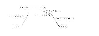
- the “heat treatment” for evaluating the HF etching rate means that the glass substrate is heated from 25° C. at a rate of 5° C./min to the temperature of the glass substrate (annealing point Ta+30° C.).
- the temperature is lowered to the temperature of (Ta - 170 ° C.) at a temperature decrease rate of 3 ° C./min, and then the temperature is decreased to 25 ° C. at a temperature decrease rate of 10 ° C./min. (see FIG. 1).
- the "annealing point Ta of the glass substrate” can be measured based on the method of ASTM C336.
- "HF etching rate” is a value measured by the following method. First, both surfaces of the sample are optically polished and then partially masked. Also, 300 mL of a 2.5 mol/L HF solution is set to 30° C. using a water bath stirrer and stirred at about 600 rpm.
- the sample is then immersed in this HF solution for 20 minutes. After that, the mask is removed, the sample is washed, and the difference in level between the masked portion and the eroded portion is measured with a surfcoder (ET4000A: manufactured by Kosaka Laboratory Co., Ltd.). Finally, the etching rate is calculated by dividing the value by the immersion time.
- a surfcoder E4000A: manufactured by Kosaka Laboratory Co., Ltd.
- the taper angle of the through-hole is determined by the ratio of the expansion speed of the hole diameter on the glass surface and the etching speed of the modified portion in the plate thickness direction.
- the former is considered to be the original etching rate of glass. Therefore, if the ratio of the two etching rates can be changed according to the thermal history of the glass, the taper angle of the through hole can be changed.
- glass physical properties change with fictive temperature.
- density, refractive index, HF etching rate, thermal contraction rate, IR spectrum, Raman spectrum, etc. change with fictive temperature.
- the fictive temperature of the original glass sheet changes greatly depending on the cooling rate during molding.
- the fictive temperature of the original glass sheet formed by the overflow downdraw method is higher than that of the original glass sheet formed by the float method.
- the fictive temperature can also be changed by annealing the molded glass substrate.
- the HF etching rate changes depending on the fictive temperature of the glass substrate, as described above. Therefore, it is presumed that the shape of the through-hole formed by performing HF etching after laser modification also changes depending on the fictive temperature. Since the fictive temperature of the glass plate changes depending on the manufacturing process of the glass plate and the subsequent annealing process, it is very important to understand the relationship between the fictive temperature and the taper angle in forming through holes in the glass plate. . However, until now, the effect of the fictive temperature of the glass substrate on the taper angle of the through-hole has not been known.
- the present inventors have focused on the above points and found that the value of ER/ERa is 1, where ER is the HF etching rate of the glass substrate (glass original plate) and ERa is the HF etching rate after heat treatment. They have found that a glass substrate having a small taper angle of the through-hole can be obtained by limiting the thickness to 0.50 or less. In particular, the inventors have found that the value of ER/ERa can be reduced by previously lowering the fictive temperature of the original glass plate by annealing or the like.
- the diameter of the through holes in the surface of the glass substrate is 1 ⁇ m to 200 ⁇ m.
- the average taper angle ⁇ in the thickness direction of the through holes is preferably 0° to 13°.
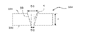
- the “average taper angle ⁇ ” is the taper angle ⁇ 1 calculated from the cross-sectional shape of the through hole from the first surface of the glass substrate to the narrowed portion of the through hole
- the taper angle ⁇ 1 It is the average value of the taper angle ⁇ 2 calculated from the cross-sectional shape of the through hole from the two sides to the narrowed portion of the through hole (see FIG. 2).
- the through-hole-forming glass substrate of the present invention is a through-hole-forming glass substrate for forming through-holes, wherein the HF etching rate of the glass substrate is ER, and the HF etching rate after heat treatment of the glass substrate is ER. is ERa, the value of ER/ERa is 1.50 or less.
- the method for manufacturing a glass substrate of the present invention includes the steps of preparing a through-hole forming glass substrate for forming through-holes, forming through-holes in the glass substrate to obtain a glass substrate having through-holes, wherein ER/ERa is 1.50 or less, where ER is the HF etching rate of the glass substrate and ERa is the HF etching rate after heat treatment of the glass substrate.
- the method for manufacturing a glass substrate of the present invention includes the steps of preparing a through-hole forming glass substrate for forming through-holes, forming through-holes in the glass substrate to obtain a glass substrate having through-holes, wherein ER/ERa is 1.50 or less, where ER is the HF etching rate of the original glass plate, and ERa is the HF etching rate after heat treatment of the original glass plate.
- the average taper angle ⁇ in the thickness direction of the through holes is 0° to 13°.
- the method for manufacturing a glass substrate of the present invention further includes a step of annealing the original glass plate.
- the “annealing step” does not include cooling treatment during the forming step, and refers to a step of raising the temperature of the glass substrate after forming from room temperature to a temperature equal to or higher than the strain point Ps and then cooling it to room temperature.
- the HF etching rate of the glass substrate is ER and the HF etching rate after heat treatment is ERa
- a coloring element or the like is introduced into the glass composition.
- a glass substrate having a through hole with a small taper angle can be obtained even without it. This results in a higher density of through-holes, which can be applied to micro-LED display applications.
- FIG. 1 is a schematic cross-sectional view showing a glass substrate having through holes according to one embodiment of the present invention
- FIG. FIG. 2 is a schematic cross-sectional view of a glass substrate before through-holes are formed
- 1 is a schematic cross-sectional view of a glass substrate having through holes according to one embodiment of the present invention
- FIG. 10 is a temperature profile of heat treatment of the alkali-free glass original plate (alkali-free glass substrate).
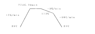
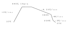
- 10 is a temperature profile of annealing of an alkali-free glass substrate according to [Example 3]. It is a temperature profile of annealing of the alkali-free glass original plate according to [Example 4]. It is a temperature profile of annealing of the alkali-free glass original plate according to [Example 5].
- the value of ER/ERa is 1.50 or less, preferably 1.40 or less. 30 or less, 1.20 or less, 1.15 or less, 1.14 or less, 1.13 or less, less than 1.12, 1.11 or less, 1.10 or less, 1.09 or less, 1.08 or less, 1. 07 or less, 1.06 or less, 1.05 or less, 1.04 or less, 1.03 or less, 1.02 or less, 1.01 or less, 1.00 or less, 0.99 or less, 0.98 or less, 0. 96 or less, especially 0.95 or less.
- the value of ER/ERa is 1.50 or less, preferably 1.40, where ER is the HF etching rate of the glass substrate and ERa is the HF etching rate after the heat treatment. 1.30 or less, 1.20 or less, 1.15 or less, 1.14 or less, 1.13 or less, less than 1.12, 1.11 or less, 1.10 or less, 1.09 or less, 1.08 1.07 or less, 1.06 or less, 1.05 or less, 1.04 or less, 1.03 or less, 1.02 or less, 1.01 or less, 1.00 or less, 0.99 or less, 0.98 Below, it is 0.96 or less, especially 0.95 or less. If ER/ERa is too large, the taper angle of the through hole will be too large.
- a method for reducing the value of ER/ERa it is effective to previously lower the fictive temperature of the glass substrate by annealing or the like, and it is particularly preferable to perform annealing, particularly off-line annealing, on the glass substrate after molding. . It is also effective to slow down the plate drawing speed during molding.
- the average taper angle ⁇ of the through holes is preferably 13° or less, 11° or less, 10° or less, 9° or less, 8° or less, particularly 7° or less. If the average taper angle ⁇ of the through-holes is too large, the diameter of the through-holes on the glass surface becomes too large, making it difficult to form the through-holes at a high density.
- the average taper angle ⁇ of the through holes is preferably 0° or more, 1° or more, 2° or more, 3° or more, or 4° or more.
- the hole diameter of the through-holes on the surface of the glass substrate is preferably 200 ⁇ m or less, 150 ⁇ m or less, 125 ⁇ m or less, 100 ⁇ m or less, 90 ⁇ m or less, 80 ⁇ m or less, 70 ⁇ m or less, 65 ⁇ m or less, 60 ⁇ m or less, 55 ⁇ m or less, 50 ⁇ m or less, 45 ⁇ m or less, 40 ⁇ m or less, 35 ⁇ m or less, particularly 30 ⁇ m or less. If the hole diameter is too large, the through holes cannot be formed on the glass substrate at high density, making it difficult to increase the pixel density of the display. On the other hand, if the hole diameter is too small, it becomes difficult to fill the inside of the hole with plating.
- the pore diameter is preferably ⁇ 1 ⁇ m, ⁇ 5 ⁇ m, ⁇ 10 ⁇ m, ⁇ 15 ⁇ m, especially ⁇ 20 ⁇ m.
- FIG. 2 is a schematic cross-sectional view showing a glass substrate having through holes according to one embodiment of the present invention.
- the average taper angle ⁇ of the through holes 20 is a value calculated from Equation 1 below.
- ⁇ ( ⁇ 1+ ⁇ 2)/2
- the taper angles ⁇ 1 and ⁇ 2 can be calculated from Equations 2 and 3 below.
- ⁇ 1 arctan(( ⁇ 1 ⁇ 3)/(2*t1)) Equation 2
- ⁇ 2 arctan(( ⁇ 2 ⁇ 3)/(2*t2)) Equation 3
- the value necessary for calculating the average taper angle ⁇ can be measured by the following method.
- the hole diameters ⁇ 1 and ⁇ 2 on the first surface 101 and the second surface 102 can be measured, for example, by observing the surface of the glass substrate with a transmission optical microscope (eg, ECLIPSE LV100ND: manufactured by NIKON) and measuring the length from the image.
- the diameter ⁇ 3 of the constricted portion of the through-hole 20, the distance t1 from the first surface 101 to the constricted portion, and the distance t2 from the second surface 102 to the constricted portion were determined by observing the through-hole 20 from the cross-sectional direction and focusing on the inside of the glass. It can be focused by moving and measured by measuring the length from the image. At this time, it is desirable to obtain a cross section by scribing the glass substrate 100 so that the through hole 20 is not exposed in the cross section and breaking the scribble.
- FIG. 3 is a schematic cross-sectional view of the original glass plate before through-holes are formed.
- the taper angles ⁇ 1 and ⁇ 2 at this time can be calculated from Equations 4 and 5 below. Using these taper angles .theta.1 and .theta.2 and Equation 1, the average taper angle .theta. can be calculated.
- ⁇ 1 arctan( ⁇ 1/(2*t1)) Equation 4
- ⁇ 2 arctan( ⁇ 2/(2*t2)) Equation 5
- the hole diameters ⁇ 1 and ⁇ 2 and the hole depths t1 and t2 on the first surface 101 and the second surface 102 can be measured from images obtained with a transmission optical microscope, as in the case of the through holes.
- FIG. 4 is a schematic cross-sectional view of a glass substrate having a through hole 20 without a constricted portion inside the glass.
- the average taper angle ⁇ at this time is defined as a value calculated from Equation (6).
- the modified portion can be formed by irradiating the glass substrate with a femtosecond or picosecond pulse laser.
- a laser wavelength of 1030 nm or less can be used.
- a Gaussian beam shape or a Bessel beam shape can be used as the laser beam shape. Among these, it is preferable to use the Bessel beam shape. If the Bessel beam shape is used, the modified portion can be formed so as to penetrate in the plate thickness direction in one shot, and the time required to fabricate the modified portion can be shortened.
- a Bessel beam shape can be formed by using, for example, an alkoxy lens.
- the type of etchant used for etching the modified portion is not particularly limited as long as the etchant has a faster etching rate for the modified portion than the glass substrate.
- HF HF
- BHF KOH
- HF is preferable because it has a high etching rate and can shorten the time required for forming through holes.
- one or a plurality of acids selected from HCl, H 2 SO 4 , HNO 3 and the like may be added to the HF solution to form a mixed solution.
- the temperature of the etchant is not particularly limited, it is effective to raise the temperature.
- the temperature range is preferably 0-50°C, more preferably 20-40°C.
- the rate of increase in the etching rate of the modified portion is greater than that of the glass substrate. Therefore, it is possible to reduce the amount of reduction in the thickness of the plate since the time required for forming the through-holes can be shortened.
- the temperature of the etchant is too high, HF volatilizes, resulting in unevenness in the concentration of HF in the etchant and increased variation in hole shape.
- the longer the etching time the larger the average taper angle ⁇ . This is for the following reasons. Residue generated by etching accumulates inside the hole during formation, and this residue inhibits etching in the direction in which the hole extends, so the taper angle of the through hole increases as the etching time increases. Therefore, the etching time is preferably 100 minutes or less, 60 minutes or less, 40 minutes or less, 30 minutes or less, especially 20 minutes or less. When the fictive temperature of the glass substrate is low, the HF etching rate is lowered, and the amount of residue generated per unit time is reduced, so that the increase speed of the taper angle can be lowered.
- the ultrasonic frequency is preferably 100 kHz or less, more preferably 45 kHz or less. If the frequency is in such a range, the effect of cavitation by ultrasonic waves can be increased.
- the glass substrate (or glass base plate) of the present invention has a glass composition of 50 to 70% by mass of SiO 2 , 12 to 25% by mass of Al 2 O 3 , 0 to 12% by mass of B 2 O 3 , and Li 2 O+Na 2 O+K. 2 O (total amount of Li 2 O, Na 2 O and K 2 O) 0 to less than 1%, MgO 0 to 8%, CaO 0 to 15%, SrO 0 to 12%, BaO 0 to 15% Among them, the following glass composition examples (1) to (4) are particularly preferred. In this way, it becomes suitable as a glass substrate for displays.
- the glass composition in mass %, is SiO 2 50 to 70%, Al 2 O 3 12 to 22% (particularly 15 to 20%), B 2 O 3 7 to 15% (particularly 6 to 10%), Li 2 O + Na 2 O + K 2 O 0 to less than 1% (especially 0 to 0.5%), MgO 0 to 3%, CaO 6 to 13% (especially 6 to 9%), SrO 0.1 to 5% (especially 0.1-3%) and BaO 3-10% (particularly 4-7%).
- SiO 2 50 to 70% SiO 2 50 to 70%, Al 2 O 3 12 to 22% (particularly 15 to 20%), B 2 O 3 7 to 15% (particularly 6 to 10%), Li 2 O + Na 2 O + K 2 O 0 to less than 1% (especially 0 to 0.5%), MgO 0 to 3%, CaO 6 to 13% (especially 6 to 9%), SrO 0.1 to 5% (especially 0.1-3%) and BaO 3-10% (particularly 4-7%).
- the glass composition, in mass %, is SiO 2 58 to 68%, Al 2 O 3 15 to 23% (particularly 17 to 21%), B 2 O 3 3 to 9% (particularly 3 to 5%), Li 2 O + Na 2 O + K 2 O 0 to less than 1% (especially 0 to 0.5%), MgO 0 to 6% (especially 1 to 4%), CaO 3 to 13% (especially 5 to 10%), SrO 0 ⁇ 10% (especially 0.1-3%) and preferably 0.1-5% BaO.
- the liquidus viscosity and Young's modulus can be increased. As a result, it becomes easy to manufacture a thin glass substrate, and it becomes easy to reduce the bending amount of the glass substrate.
- SiO 2 60 to 70% (especially 65 to 70%), Al 2 O 3 7 to 20% (especially 7 to 16%), B 2 O 3 0 to 8% ( Li 2 O+Na 2 O+K 2 O 0-1% (especially 0-0.5%), MgO 0-10% (especially 0.1-5%), CaO 0-7%, It preferably contains 0-7% SrO and 0-15% BaO. This makes it easier to lower the HF etching rate. As a result, it becomes easier to reduce the amount of residue generated when forming through-holes by HF etching, and it becomes easier to reduce the taper angle of the through-holes.
- the glass substrate (original glass plate) of the present invention preferably has the following properties.
- the average coefficient of thermal expansion in the temperature range of 30 to 380° C. is preferably 30 ⁇ 10 ⁇ 7 to 50 ⁇ 10 ⁇ 7 /° C., more preferably 32 ⁇ 10 ⁇ 7 to 48 ⁇ 10 ⁇ 7 /° C., more preferably 33 ⁇ 10 -7 to 45 ⁇ 10 -7 /°C, more preferably 34 ⁇ 10 -7 to 44 ⁇ 10 -7 /°C, particularly preferably 35 ⁇ 10 -7 to 43 ⁇ 10 -7 /°C.
- the "average coefficient of thermal expansion in the temperature range of 30 to 380°C" is a value measured with a dilatometer.
- the Young's modulus is preferably 65 GPa or higher, more preferably 70 GPa or higher, more preferably 75 GPa or higher, more preferably 77 GPa or higher, and particularly preferably 78 GPa or higher. If the Young's modulus is too low, defects due to bending of the glass substrate are likely to occur. "Young's modulus” refers to a value measured by a well-known resonance method.
- the strain point is preferably 650°C or higher, more preferably 680°C or higher, more preferably higher than 686°C, and particularly preferably 690°C or higher. In this way, thermal contraction of the glass substrate can be suppressed in the TFT manufacturing process.
- the "strain point" is a value measured according to the ASTM C336 method.
- the liquidus temperature is preferably 1350°C or lower, more preferably less than 1350°C, more preferably 1300°C or lower, and particularly preferably 1000 to 1280°C.
- the liquidus viscosity is preferably 10 4.0 dPa ⁇ s or more, more preferably 10 4.1 dPa ⁇ s or more, more preferably 10 4.2 dPa ⁇ s or more, and particularly preferably 10 4.3 dPa ⁇ s. That's it. By doing so, it becomes easy to prevent a situation in which devitrified crystals are generated during molding and productivity is lowered.
- the liquidus temperature is an index of devitrification resistance, and the lower the liquidus temperature, the better the devitrification resistance.
- “Liquidus temperature” is the temperature at which crystals precipitate after passing through a 30-mesh (500 ⁇ m) standard sieve and remaining on the 50-mesh (300 ⁇ m) glass powder in a platinum boat and holding it in a temperature gradient furnace for 24 hours. is.
- the "liquidus viscosity” is a value obtained by measuring the viscosity of the glass at the liquidus temperature TL by the platinum ball pull-up method.
- the temperature at a high temperature viscosity of 10 2.5 dPa ⁇ s is preferably 1700°C or lower, more preferably 1690°C or lower, more preferably 1680°C or lower, and particularly preferably 1400 to 1670°C. If the temperature at the high-temperature viscosity of 10 2.5 dPa ⁇ s is too high, it becomes difficult to melt the glass batch, and the manufacturing cost of the glass substrate rises.
- the temperature at a high-temperature viscosity of 10 2.5 dPa ⁇ s corresponds to the melting temperature, and the lower the temperature, the better the meltability. Also, the "temperature at a high temperature viscosity of 10 2.5 dPa ⁇ s" can be measured by, for example, a platinum ball pull-up method.
- the glass substrate (original glass plate) of the present invention is preferably formed by an overflow down-draw method.
- the overflow down-draw method molten glass is overflowed from both sides of a heat-resistant trough-shaped structure, and while the overflowing molten glass is joined at the lower end of the trough-shaped structure, it is stretched downward to produce a glass substrate.
- the method In the overflow down-draw method, the surface to be the surface of the original glass sheet does not come into contact with the gutter-shaped refractory and is molded in a free surface state. Therefore, an unpolished glass substrate having good surface quality can be manufactured at low cost, and thinning is easy.
- the plate thickness is not particularly limited, but preferably less than 0.7 mm, 0.6 mm or less, less than 0.6 mm, particularly 0.05 to 0.5 mm.
- the smaller the plate thickness the smaller the hole diameter of the through hole. As a result, through-holes can be produced at high density.
- the plate thickness can be adjusted by adjusting the flow rate during molding, the plate drawing speed, and the like.
- the glass substrate of the present invention is preferably used as a substrate for a micro LED display, particularly a tiling micro LED display.
- a micro LED display particularly a tiling micro LED display.
- the light-emitting elements on the glass surface can be driven from the back surface of the glass by establishing conduction between the front and back surfaces of the glass substrate through the through holes.
- through holes can be formed at a high density, so that a tiling-type micro LED display can be made with high definition.
- a method for manufacturing a glass substrate of the present invention includes the steps of preparing a glass substrate for forming through holes, and forming through holes in the glass substrate to obtain a glass substrate having through holes.
- the value of ER/ERa is 1.50 or less, where ER is the HF etching rate of the glass substrate and ERa is the HF etching rate after the glass substrate is heat-treated.
- a method for manufacturing a glass substrate of the present invention comprises the steps of preparing a glass substrate for forming through holes, and forming through holes in the glass substrate to obtain a glass substrate having through holes.
- the value of ER/ERa is 1.50 or less, where ER is the etching rate and ERa is the HF etching rate after heat treatment of the glass substrate.
- a method for reducing the value of ER/ERa it is effective to previously lower the fictive temperature of the glass substrate by annealing or the like, and it is particularly preferable to perform annealing, particularly off-line annealing, on the glass substrate after molding. . It is also effective to slow down the plate drawing speed during molding.
- annealing particularly off-line annealing
- Example 1 First, a non-alkali glass substrate (manufactured by Nippon Electric Glass Co., Ltd., trade name OA-11, annealing point Ta 743° C.) with a thickness of 500 ⁇ m was prepared and annealed from room temperature (25° C.) along the temperature profile shown in FIG. The density and HF etching rate (ER) of this alkali-free glass substrate were measured. Further, this alkali-free glass substrate was heat-treated from room temperature (25° C.) along the temperature profile shown in FIG. 5, and the HF etching rate (ERa) was measured.
- ER HF etching rate
- the density is a value measured by the well-known Archimedes method.
- HF etching rate is a value measured by the following method. First, both surfaces of the sample were optically polished and then partially masked. 300 mL of a 2.5 mol/L HF solution was set to 30° C. using a water bath stirrer and stirred at about 600 rpm. An alkali-free glass substrate was immersed in this HF solution for 20 minutes. After that, the mask was removed, the sample was washed, and the difference in level between the masked portion and the eroded portion was measured with a surfcoder (ET4000A: manufactured by Kosaka Laboratory Co., Ltd.). The etching rate was calculated by dividing the value by the immersion time.
- a surfcoder E4000A: manufactured by Kosaka Laboratory Co., Ltd.
- through-holes were formed in the glass substrate annealed with the temperature profile shown in FIG. 5 by the following method to obtain a glass substrate having through-holes.
- a picosecond pulse laser shaped into a Bessel beam shape was irradiated to an alkali-free glass original plate cut into a rectangular shape of 40 mm ⁇ 20 mm so that the pitch interval was about 200 ⁇ m, and about 8000 pieces were irradiated on the alkali-free glass original plate. formed a reformed part.
- the alkali-free glass original plate was etched by wet etching under the following conditions. Etching times were 15 minutes and 30 minutes. An alkali-free glass original plate was placed in a PP test tube containing an etchant, and etching was performed by applying ultrasonic waves to the etchant. At this time, using a Teflon jig, the alkali-free glass original plate was fixed with a distance of 10 mm from the bottom of the test tube. As an etchant, an etchant containing 2.5 mol/L of HF and 1.0 mol/L of HCL was used. The temperature of the etchant was 30°C.
- a chiller was used to circulate the water in the ultrasonic device and keep the water temperature at 30°C.
- An ultrasonic cleaning machine (VS-100III: manufactured by AS ONE CORPORATION) was used to apply ultrasonic vibration, and ultrasonic waves of 28 kHz were applied to the etchant.
- the taper angle of the hole thus formed was determined by the method described above.
- Example 2 A 500 ⁇ m-thick alkali-free glass substrate (manufactured by Nippon Electric Glass Co., Ltd., trade name OA-11) was prepared, and the density and HF etching rate (ER) were measured without annealing. Furthermore, this glass substrate was heat-treated from room temperature (25° C.) along the temperature profile shown in FIG. 5, and the HF etching rate (ERa) was measured. Further, holes were formed in the same manner as in Example 1 for this glass substrate (not heat-treated).
- ER density and HF etching rate
- Table 1 shows the densities and HF etching rates of the glass substrates according to Examples 1 and 2
- Table 2 shows the hole shapes of the glass substrates according to Examples 1 and 2.
- the value of ER/ERa was evaluated for the alkali-free glass original plate in which no holes were formed.
- the ER and ERa values were 0.89, and the ER/ERa value was 1.00.
- the ER/ERa value was evaluated for the alkali-free glass substrate according to Example 2 after forming the through holes (the glass substrate having the through holes that were not heat-treated)
- the ER value was 1.00
- the ERa value was 1.00.
- Example 3 First, a non-alkali glass substrate (manufactured by Nippon Electric Glass Co., Ltd., trade name OA-11, annealing point Ta 743° C.) with a thickness of 500 ⁇ m was prepared and annealed from room temperature (25° C.) along the temperature profile shown in FIG. The HF etching rate (ER) of this alkali-free glass substrate was measured. Further, this alkali-free glass substrate was heat-treated from room temperature (25° C.) along the temperature profile shown in FIG. 5, and the HF etching rate (ERa) was measured. Further, holes were formed in the same manner as in Example 1 for this glass substrate (annealed but not heat-treated).
- ER HF etching rate
- Example 4 First, a non-alkali glass substrate (manufactured by Nippon Electric Glass Co., Ltd., trade name OA-11, annealing point Ta 743° C.) having a thickness of 500 ⁇ m was prepared and annealed from room temperature (25° C.) along the temperature profile shown in FIG. The HF etching rate (ER) of this alkali-free glass substrate was measured. Further, this alkali-free glass substrate was heat-treated from room temperature (25° C.) along the temperature profile shown in FIG. 5, and the HF etching rate (ERa) was measured. Further, holes were formed in the same manner as in Example 1 for this glass substrate (annealed but not heat-treated).
- ER HF etching rate
- Example 5 First, an alkali-free glass substrate (manufactured by Nippon Electric Glass Co., Ltd., trade name OA-11, annealing point Ta 743° C.) with a thickness of 500 ⁇ m was prepared and annealed from room temperature (25° C.) along the temperature profile shown in FIG. The HF etching rate (ER) of this alkali-free glass substrate was measured. Further, this alkali-free glass substrate was heat-treated from room temperature (25° C.) along the temperature profile shown in FIG. 5, and the HF etching rate (ERa) was measured. Further, holes were formed in the same manner as in Example 1 for this glass substrate (annealed but not heat-treated).
- ER HF etching rate
- Table 3 shows the HF etching rates of the glass substrates according to Examples 3-5, and also shows the hole shapes of the glass substrates according to Examples 3-5.
- the value of ER/ERa was evaluated for the alkali-free glass original plate in which no holes were formed.
- the ER value was 0.93
- the ERa value was 0.89
- the ER/ERa value was 1.04.
- the ER/ERa value was evaluated for the alkali-free glass substrate according to Example 4 after forming the through holes (the glass substrate having the through holes that were not heat-treated)
- the ER value was 0.94.
- the ERa value was 0.89 and the ER/ERa value was 1.06.
- the ER/ERa value was evaluated for the alkali-free glass substrate according to Example 5 after forming the through holes (the glass substrate having the through holes that were not heat-treated).
- the ER value was 0.97.
- the ERa value was 0.89 and the ER/ERa value was 1.09.
- the holes formed in the glass substrate were non-penetrating. It can be read from Tables 1 to 3 that the average taper angle ⁇ of the holes can be reduced by this. According to Table 3, when annealing the original glass plate for forming the through-holes, it is preferable that the cooling rate during annealing is slow. This result indicates that the taper angle of the through-hole can be reduced by adjusting the molding conditions such as lowering the plate drawing speed than usual during molding by the overflow down-draw method without performing off-line annealing. showing.
Landscapes
- Engineering & Computer Science (AREA)
- Chemical & Material Sciences (AREA)
- Chemical Kinetics & Catalysis (AREA)
- General Chemical & Material Sciences (AREA)
- Geochemistry & Mineralogy (AREA)
- Materials Engineering (AREA)
- Organic Chemistry (AREA)
- Life Sciences & Earth Sciences (AREA)
- Physics & Mathematics (AREA)
- Theoretical Computer Science (AREA)
- General Physics & Mathematics (AREA)
- Microelectronics & Electronic Packaging (AREA)
- Thermal Sciences (AREA)
- Manufacturing & Machinery (AREA)
- Surface Treatment Of Glass (AREA)
- Glass Compositions (AREA)
- Re-Forming, After-Treatment, Cutting And Transporting Of Glass Products (AREA)
Abstract
本発明のガラス基板は、貫通孔を有するガラス基板において、ガラス基板のHFエッチングレートをER、そのガラス基板を熱処理した後のHFエッチングレートをERaとした時に、ER/ERaの値が1.50以下になることを特徴とする。
Description
本発明はガラス基板、貫通孔形成用ガラス原板及びガラス基板の製造方法に関する。具体的には、エッチングにより形成された貫通孔を有するガラス基板、貫通孔形成用ガラス原板及び貫通孔を有するガラス基板の製造方法に関する。
貫通孔を有するガラス基板は、例えば、ガラスインターポーザーやマイクロLEDディスプレイに使用されている(特許文献1、2参照)。これらの用途では、ガラス基板の表面における貫通孔の孔径が小さい程、貫通孔を高密度に作製し得るため、ガラス基板上に半導体を高密度に実装することができる。
貫通孔を形成する第一の方法として、ガラス原板にレーザー光を照射して貫通孔を形成する方法が知られている(特許文献3参照)。第二の方法として、レーザーにより初期貫通孔を形成した後、エッチングにより孔径を拡大する方法も提案されている(特許文献4参照)。
しかし、これら第一及び第二の方法は、レーザーによる熱加工により貫通孔を形成しているため、ガラス基板にクラック等が生じる問題があった。
そこで、第三の方法として、レーザー光の照射により改質部を作製した後、エッチングにより改質部を除去することで貫通孔を形成する方法が検討されている(特許文献5参照)。そして、改質部の作製には、超短パルスレーザーが用いられるため、熱影響を限りなく小さくすることができ、前述したような問題が発生しない。
また、第三の方法で貫通孔を作製する場合、厚み方向で貫通孔がテーパー形状を有する。貫通孔を高密度で作製するためには貫通孔のテーパー角を小さくすることが重要であり、そのために例えばガラスに着色元素を添加することが提案されている(特許文献6参照)。
ところで、ディスプレイ用途では無アルカリガラスが広く使用されている。しかし、無アルカリガラスに対して、第三の方法で貫通孔を形成すると、貫通孔のテーパー角が大きくなり、孔密度を高くすることができなかった。そのため、マイクロLEDディスプレイの用途に適用することができなかった。
特許文献6の記載のように、貫通孔のテーパー角を小さくするために、ガラス組成中に着色元素を添加することが考えられる。しかし、着色元素を添加すると、従来のガラスに比べて、物理的特性、化学的特性、光学的特性が大きく変動し、例えばパネルメーカーにおける成膜工程等において、成膜条件等の調整が困難になる。
本発明の目的は、ディスプレイ用途に使用可能であり、且つ貫通孔のテーパー角が小さいガラス基板及びその製造方法を提供すると共に、貫通孔のテーパー角を低減し得る貫通孔形成用ガラス原板を提供することである。
本発明者は、鋭意検討の結果、熱処理した後のエッチングレート比を所定値以下に規制することにより、上記技術的課題を解決し得ることを見出し、本発明として提案するものである。すなわち、本発明のガラス基板は、貫通孔を有するガラス基板において、ガラス基板のHFエッチングレートをER、そのガラス基板を熱処理した後のHFエッチングレートをERaとした時に、ER/ERaの値が1.50以下になることを特徴とする。ここで、HFエッチングレートを評価するための「熱処理」とは、ガラス基板に対して、25℃から5℃/分の昇温速度でガラス基板の(徐冷点Ta+30℃)の温度まで昇温し、(Ta+30℃)の温度で30分間保持した後、3℃/分の降温速度で(Ta-170℃)の温度まで降温し、その後10℃/分の降温速度で25℃まで降温することである(図1参照)。「ガラス基板の徐冷点Ta」は、ASTM C336の方法に基づいて測定することができる。「HFエッチングレート」は、以下の方法により測定した値である。まず試料の両面を光学研磨した後、一部をマスキングする。また、2.5mоl/LのHF溶液300mLについて、ウォーターバススターラーを用いて30℃に設定し、約600rpmで撹拌する。次に、このHF溶液中に試料を20分間浸漬させる。その後、マスクを除去し、試料を洗浄し、マスク部分と浸食部分の段差をサーフコーダ(ET4000A:小坂研究所社製)で測定する。最後に、その値を浸漬時間で除することでエッチングレートを算出する。
第三の方法で貫通孔を形成する場合、貫通孔のテーパー角は、ガラス表面における孔径の拡大速度と改質部の板厚方向のエッチング速度との比により決まる。ここで、前者はガラス本来のエッチング速度と考えられる。そのため、ガラスの熱履歴によって二種類のエッチング速度の比を変えることができれば、貫通孔のテーパー角を変化させることができる。
ところで、ガラス物性は仮想温度により変化し、例えば密度、屈折率、HFエッチングレート、熱収縮率、IRスペクトル、ラマンスペクトルなどは、仮想温度により変化する。仮想温度が低くなると、密度が大きくなり、またHFエッチングレートは低くなる。そのため、密度やHFエッチングレートは、仮想温度を表す指標として用いることができる。
ガラス原板の仮想温度は、成形時の冷却速度により大きく変化し、例えばオーバーフローダウンドロー法により成形されたガラス原板の仮想温度は、フロート法により成形されたガラス原板よりも仮想温度が高くなる。また、成形後のガラス原板に対してアニールを行うことによっても仮想温度を変化させることができる。
HFエッチングレートは、上記の通り、ガラス原板の仮想温度により変化する。よって、レーザー改質した後にHFエッチングを行うことで形成される貫通孔の形状も仮想温度によって変化することが推定される。ガラス原板の製造工程やその後のアニール工程により、ガラス原板の仮想温度は変化するため、仮想温度とテーパー角の関係を把握することは、ガラス原板に貫通孔を形成する上で非常に重要である。しかしながら、ガラス原板の仮想温度が貫通孔のテーパー角に与える影響については現在まで知られていなかった。
本発明者は、鋭意検討の結果、上記点に着目した上で、ガラス基板(ガラス原板)のHFエッチングレートをER、熱処理後のHFエッチングレートをERaとした時に、ER/ERaの値を1.50以下に規制することにより、貫通孔のテーパー角が小さいガラス基板が得られることを見出したものである。特に、アニール等によって予めガラス原板の仮想温度を低くすると、ER/ERaの値を低減し得ることを見出したものである。
また、本発明のガラス基板は、ガラス基板の表面における貫通孔の孔直径が1μm~200μmであることが好ましい。
また、本発明のガラス基板は、貫通孔の厚み方向の平均テーパー角θが0°~13°であることが好ましい。ここで、「平均テーパー角θ」とは、ガラス基板の第一面から貫通孔の狭窄部までの貫通孔の断面形状から計算されるテーパー角θ1と、ガラス基板の第一面と対向する第二面から貫通孔の狭窄部までの貫通孔の断面形状から計算されるテーパー角θ2の平均値である(図2参照)。
また、本発明の貫通孔形成用ガラス原板は、貫通孔を形成するための貫通孔形成用ガラス原板であって、ガラス原板のHFエッチングレートをER、そのガラス原板を熱処理した後のHFエッチングレートをERaとした時に、ER/ERaの値が1.50以下になることを特徴とする。
本発明のガラス基板の製造方法は、貫通孔を形成するための貫通孔形成用ガラス原板を用意する工程と、ガラス原板に貫通孔を形成して、貫通孔を有するガラス基板を得る工程と、を備え、ガラス基板のHFエッチングレートをER、そのガラス基板を熱処理した後のHFエッチングレートをERaとした時に、ER/ERaの値が1.50以下になることを特徴とする。
本発明のガラス基板の製造方法は、貫通孔を形成するための貫通孔形成用ガラス原板を用意する工程と、ガラス原板に貫通孔を形成して、貫通孔を有するガラス基板を得る工程と、を備え、ガラス原板のHFエッチングレートをER、そのガラス原板を熱処理した後のHFエッチングレートをERaとした時に、ER/ERaの値が1.50以下になることを特徴とする。
また、本発明のガラス基板の製造方法は、貫通孔の厚み方向の平均テーパー角θが0°~13°であることが好ましい。
また、本発明のガラス基板の製造方法は、ガラス原板をアニールする工程を更に備えることが好ましい。ここで、「アニールする工程」とは、成形工程時の冷却処理を含まず、成形後のガラス原板を室温から歪点Ps以上の温度まで昇温した後、室温まで降温する工程を指す。
本発明によれば、ガラス基板のHFエッチングレートをER、熱処理後のHFエッチングレートをERaとした時に、ER/ERaの値を1.50以下に規制すると、ガラス組成中に着色元素等を導入しなくても、貫通孔のテーパー角が小さいガラス基板を得ることができる。これにより、貫通孔の高密度が高くなり、マイクロLEDディスプレイの用途に適用することができる。
本発明のガラス基板において、ガラス基板のHFエッチングレートをER、熱処理後のHFエッチングレートをERaとした時に、ER/ERaの値は1.50以下であり、好ましくは1.40以下、1.30以下、1.20以下、1.15以下、1.14以下、1.13以下、1.12未満、1.11以下、1.10以下、1.09以下、1.08以下、1.07以下、1.06以下、1.05以下、1.04以下、1.03以下、1.02以下、1.01以下、1.00以下、0.99以下、0.98以下、0.96以下、特に0.95以下である。本発明の貫通孔形成用ガラス原板において、ガラス原板のHFエッチングレートをER、熱処理後のHFエッチングレートをERaとした時に、ER/ERaの値は1.50以下であり、好ましくは1.40以下、1.30以下、1.20以下、1.15以下、1.14以下、1.13以下、1.12未満、1.11以下、1.10以下、1.09以下、1.08以下、1.07以下、1.06以下、1.05以下、1.04以下、1.03以下、1.02以下、1.01以下、1.00以下、0.99以下、0.98以下、0.96以下、特に0.95以下である。ER/ERaが大き過ぎると、貫通孔のテーパー角が大きくなり過ぎる。
ER/ERaの値を低減する方法として、アニール等によって予めガラス原板の仮想温度を低くすることが有効であり、特に成形後のガラス原板について、アニールを行うこと、特にオフラインアニールを行うことが好ましい。また成形時の板引き速度を遅くすることも有効である。
本発明のガラス基板において、貫通孔の平均テーパー角θは、好ましくは13°以下、11°以下、10°以下、9°以下、8°以下、特に7°以下である。貫通孔の平均テーパー角θが大き過ぎると、ガラス表面における貫通孔の孔径が大きくなり過ぎて、貫通孔を高密度に作製することが困難になる。
第三の方法でガラス原板に貫通孔を形成して、貫通孔を有するガラス基板を作製する後、ガラス基板の表裏面の導通を取るため、貫通孔内壁に導電部を形成するためのメッキ工程が必要となる。貫通孔の平均テーパー角θが小さ過ぎると、このメッキ工程で、スパッタによるシード層を作製する時に貫通孔の深い位置まで成膜することが困難になる。よって、貫通孔の平均テーパー角θは0°以上、1°以上、2°以上、3°以上、4°以上であることが好ましい。
ガラス基板の表面における貫通孔の孔直径は、好ましくは200μm以下、150μm以下、125μm以下、100μm以下、90μm以下、80μm以下、70μm以下、65μm以下、60μm以下、55μm以下、50μm以下、45μm以下、40μm以下、35μm以下、特に30μm以下である。孔直径が大き過ぎると、ガラス基板上に貫通孔を高密度に形成できなくなり、ディスプレイの画素密度を高め難くなる。一方、孔直径が小さ過ぎると、孔内部にメッキを充填することが難しくなる。よって、孔直径は、好ましくは1μm以上、5μm以上、10μm以上、15μm以上、特に20μm以上である。
次に、貫通孔のテーパー角の評価方法について説明する。
図2は、本発明の一実施形態の貫通孔を有するガラス基板を示す模式的断面図である。図2において、貫通孔20の平均テーパー角θは、以下の式1から計算される値である。
θ=(θ1+θ2)/2 ・・・ 式1
また、テーパー角θ1及びθ2は、以下の式2及び式3から計算することができる。
θ1=arctan((Φ1―Φ3)/(2*t1)) ・・・ 式2
θ2=arctan((Φ2―Φ3)/(2*t2)) ・・・ 式3
図2は、本発明の一実施形態の貫通孔を有するガラス基板を示す模式的断面図である。図2において、貫通孔20の平均テーパー角θは、以下の式1から計算される値である。
θ=(θ1+θ2)/2 ・・・ 式1
また、テーパー角θ1及びθ2は、以下の式2及び式3から計算することができる。
θ1=arctan((Φ1―Φ3)/(2*t1)) ・・・ 式2
θ2=arctan((Φ2―Φ3)/(2*t2)) ・・・ 式3
平均テーパー角θの計算に必要な値は、以下の方法により測定できる。第一面101及び第二面102における孔径Φ1、Φ2は、例えばガラス基板の表面を透過型光学顕微鏡(例えばECLIPSE LV100ND:NIKON社製)により観察し、画像から測長することで測定できる。貫通孔20の狭窄部の直径Φ3、第一面101から狭窄部までの距離t1及び第二面102から狭窄部までの距離t2は、貫通孔20を断面方向から観察し、焦点をガラス内部に移動することで焦点を合わせ、画像から測長することで測定できる。この際、貫通孔20が断面に露出しないようにガラス基板100にスクライブを入れ、これを折り割ることで断面を得ることが望ましい。
また、非貫通孔であっても同様に平均テーパー角θを計算することができる。図3は、貫通孔が形成される前のガラス原板の模式的断面図である。この時のテーパー角θ1及びθ2は、以下の式4及び式5から計算することができる。このテーパー角θ1及びθ2と式1を用いて平均テーパー角θを計算することができる。
θ1=arctan(Φ1/(2*t1)) ・・・ 式4
θ2=arctan(Φ2/(2*t2)) ・・・ 式5
θ1=arctan(Φ1/(2*t1)) ・・・ 式4
θ2=arctan(Φ2/(2*t2)) ・・・ 式5
第一面101及び第二面102における孔径Φ1、Φ2及び孔深さt1、t2は、貫通孔の場合と同様に、透過型光学顕微鏡で得た画像から測長することができる。
第一面101及び第二面102における孔径Φ1、Φ2及び孔深さt1、t2は、貫通孔の場合と同様に、また、貫通孔20がガラス内部に狭窄部を持たない場合、平均テーパー角θは以下のように定義される。図4はガラス内部に狭窄部を持たない貫通孔20を有するガラス基板の模式的断面図である。この時の平均テーパー角θは、式6から計算される値として定義される。第一面101及び第二面102における孔径Φ1、Φ2及び板厚tは、上記の場合と同様に、透過型光学顕微鏡を用いて得た画像から測長することで測定できる。
θ=arctan((Φ1―θ2)/(2*t)) ・・・ 式6
θ=arctan((Φ1―θ2)/(2*t)) ・・・ 式6
次に、ガラス原板に貫通孔を形成する方法について説明する。改質部はガラス原板にフェムト秒又はピコ秒パルスレーザーを照射することにより形成することができる。レーザー波長は、1030nm以下の波長を用いることができる。
なお、レーザーのビーム形状としては、ガウシアンビーム形状又はベッセルビーム形状を用いることができる。この内、ベッセルビーム形状を用いることが好ましい。ベッセルビーム形状とすれば、ワンショットで板厚方向に貫くように改質部を形成することができ、改質部の作製に必要な時間を短縮することができる。ベッセルビーム形状は、例えばアルコキシレンズを用いることで形成することができる。
改質部のエッチングに用いるエッチング液の種類は、ガラス原板よりも改質部のエッチングレートが速いエッチング液であれば特に限定されず、例えばHF、BHF,KOH等を使用することができる。特に、エッチングレートが速く、貫通孔の形成にかかる時間を短縮し得るため、HFが好ましい。また、HF溶液に対して、HCl、H2SO4、HNO3などの酸から一つ又は複数種類選び、これを加えた混合溶液としてもよい。
エッチング液の温度は特に限定されないが、温度を高くすることが有効である。HFを含むエッチング液の場合、その温度範囲は好ましくは0~50℃であり、より好ましくは20~40℃である。エッチング液の温度を高くすると、ガラス原板よりも改質部のエッチング速度の増加の割合の方が大きくなる。そのため、貫通孔の作製にかかる時間を短縮し得るため、板厚の減少量を小さくすることができる。一方、エッチング液の温度が高過ぎると、HFが揮発して、エッチング液中でのHFの濃度ムラが生じ、孔形状のばらつきが大きくなる。
エッチング時間が長い程、平均テーパー角θが大きくなる。これは、以下の理由に依るものである。エッチングにより生じた残渣が形成途中の孔内部に堆積し、この残渣が孔の伸展する方向のエッチングを阻害するため、エッチング時間が長くなるにつれて貫通孔のテーパー角が増加していく。よって、エッチング時間は、好ましくは100分間以下、60分間以下、40分間経過、30分間以下、特に20分間以下である。なお、ガラス原板の仮想温度を低いと、HFエッチングレートが低下し、単位時間辺りに生じる残渣量が低減されるため、テーパー角の増加速度を低下させることができる。
ガラス原板のエッチングの際に、エッチング液の撹拌又は超音波を印加することが好ましい。特に超音波の印加により、孔内壁への残渣の固着及び再付着を抑制することができる。超音波の周波数は、好ましくは100kHz以下であり、より好ましくは45kHz以下である。このような範囲の周波数であれば、超音波によるキャビテーションの効果を大きくすることができる。
本発明のガラス基板(又はガラス原板)は、ガラス組成として、質量%で、SiO2 50~70%、Al2O3 12~25%、B2O3 0~12%、Li2O+Na2O+K2O(Li2O、Na2O及びK2Oの合量) 0~1%未満、MgO 0~8%、CaO 0~15%、SrO 0~12%、BaO 0~15%を含有することが好ましく、その中でも、以下のガラス組成例(1)~(4)が特に好ましい。このようにすれば、ディスプレイ用ガラス基板として好適になる。
(1)ガラス組成として、質量%で、SiO2 50~70%、Al2O3 12~22%(特に15~20%)、B2O3 7~15%(特に6~10%)、Li2O+Na2O+K2O 0~1%未満(特に0~0.5%)、MgO 0~3%、CaO 6~13%(特に6~9%)、SrO 0.1~5%(特に0.1~3%)、BaO 3~10%(特に4~7%)を含有することが好ましい。このようにすれば、溶融温度を低下させつつ、液相粘度を高めることができる。結果として、ガラス基板の製造コストを低廉化することができる。
(2)ガラス組成として、質量%で、SiO2 58~68%、Al2O3 15~23%(特に17~21%)、B2O3 3~9%(特に3~5%)、Li2O+Na2O+K2O 0~1%未満(特に0~0.5%)、MgO 0~6%(特に1~4%)、CaO 3~13%(特に5~10%)、SrO 0~10%(特に0.1~3%)、BaO 0.1~5%を含有することが好ましい。このようにすれば、液相粘度とヤング率を高めることができる。結果として、薄肉のガラス基板を作製し易くなり、更にそのガラス基板の撓み量を低減し易くなる。
(3)ガラス組成として、質量%で、SiO2 58~65%、Al2O3 18~23%、B2O3 0~3%(特に0.1~1%未満)、Li2O+Na2O+K2O 0~1%未満(特に0~0.5%)、MgO 0.1~6%(特に2~5%)、CaO 2~7%(特に4~6%)、SrO 0~5%、BaO 2~15%(特に5~10%)を含有することが好ましい。このようにすれば、歪点を730℃以上に高め易くなる。
(4)ガラス組成として、質量%で、SiO2 60~70%(特に65~70%)、Al2O3 7~20%(特に7~16%)、B2O3 0~8%(特に2~8%)、Li2O+Na2O+K2O 0~1%未満(特に0~0.5%)、MgO 0~10%(特に0.1~5%)、CaO 0~7%、SrO 0~7%、BaO 0~15%を含有することが好ましい。このようにすれば、HFエッチングレートを低くし易くなる。結果として、HFエッチングにより貫通孔を作製する際に生じる残渣量を低減し易くなり、貫通孔のテーパー角を低減し易くなる。
(1)ガラス組成として、質量%で、SiO2 50~70%、Al2O3 12~22%(特に15~20%)、B2O3 7~15%(特に6~10%)、Li2O+Na2O+K2O 0~1%未満(特に0~0.5%)、MgO 0~3%、CaO 6~13%(特に6~9%)、SrO 0.1~5%(特に0.1~3%)、BaO 3~10%(特に4~7%)を含有することが好ましい。このようにすれば、溶融温度を低下させつつ、液相粘度を高めることができる。結果として、ガラス基板の製造コストを低廉化することができる。
(2)ガラス組成として、質量%で、SiO2 58~68%、Al2O3 15~23%(特に17~21%)、B2O3 3~9%(特に3~5%)、Li2O+Na2O+K2O 0~1%未満(特に0~0.5%)、MgO 0~6%(特に1~4%)、CaO 3~13%(特に5~10%)、SrO 0~10%(特に0.1~3%)、BaO 0.1~5%を含有することが好ましい。このようにすれば、液相粘度とヤング率を高めることができる。結果として、薄肉のガラス基板を作製し易くなり、更にそのガラス基板の撓み量を低減し易くなる。
(3)ガラス組成として、質量%で、SiO2 58~65%、Al2O3 18~23%、B2O3 0~3%(特に0.1~1%未満)、Li2O+Na2O+K2O 0~1%未満(特に0~0.5%)、MgO 0.1~6%(特に2~5%)、CaO 2~7%(特に4~6%)、SrO 0~5%、BaO 2~15%(特に5~10%)を含有することが好ましい。このようにすれば、歪点を730℃以上に高め易くなる。
(4)ガラス組成として、質量%で、SiO2 60~70%(特に65~70%)、Al2O3 7~20%(特に7~16%)、B2O3 0~8%(特に2~8%)、Li2O+Na2O+K2O 0~1%未満(特に0~0.5%)、MgO 0~10%(特に0.1~5%)、CaO 0~7%、SrO 0~7%、BaO 0~15%を含有することが好ましい。このようにすれば、HFエッチングレートを低くし易くなる。結果として、HFエッチングにより貫通孔を作製する際に生じる残渣量を低減し易くなり、貫通孔のテーパー角を低減し易くなる。
本発明のガラス基板(ガラス原板)は、以下の特性を有することが好ましい。
30~380℃の温度範囲における平均熱膨張係数は、好ましくは30×10-7~50×10-7/℃、より好ましくは32×10-7~48×10-7/℃、より好ましくは33×10-7~45×10-7/℃、より好ましくは34×10-7~44×10-7/℃、特に好ましくは35×10-7~43×10-7/℃である。このようにすれば、TFTに使用されるSiの熱膨張係数に整合し易くなる。なお、「30~380℃の温度範囲における平均熱膨張係数」は、ディラトメーターで測定した値である。
ヤング率は、好ましくは65GPa以上、より好ましくは70GPa以上、より好ましくは75GPa以上、より好ましくは77GPa以上、特に好ましくは78GPa以上である。ヤング率が低過ぎると、ガラス基板の撓みに起因した不具合が発生し易くなる。なお、「ヤング率」は、周知の共振法で測定した値を指す。
歪点は、好ましくは650℃以上、より好ましくは680℃以上、より好ましくは686℃超、特に好ましくは690℃以上である。このようにすれば、TFT製造プロセスにおいて、ガラス基板の熱収縮を抑制することができる。なお、「歪点」は、ASTM C336の方法に基づいて測定した値である。
液相温度は、好ましくは1350℃以下、より好ましくは1350℃未満、より好ましくは1300℃以下、特に好ましくは1000~1280℃である。液相粘度は、好ましくは104.0dPa・s以上、より好ましくは104.1dPa・s以上、より好ましくは104.2dPa・s以上、特に好ましくは104.3dPa・s以上である。このようにすれば、成形時に失透結晶が発生して、生産性が低下する事態を防止し易くなる。更にオーバーフローダウンドロー法で成形し易くなるため、ガラス基板の表面品位を高め易くなると共に、ガラス基板の製造コストを低廉化することができる。なお、液相温度は、耐失透性の指標であり、液相温度が低い程、耐失透性に優れる。「液相温度」は、標準篩30メッシュ(500μm)を通過し、50メッシュ(300μm)に残るガラス粉末を白金ボートに入れて、温度勾配炉中に24時間保持した後、結晶が析出する温度である。「液相粘度」は、液相温度TLにおけるガラスの粘度を白金球引き上げ法で測定した値である。
高温粘度102.5dPa・sにおける温度は、好ましくは1700℃以下、より好ましくは1690℃以下、より好ましくは1680℃以下、特に好ましくは1400~1670℃である。高温粘度102.5dPa・sにおける温度が高過ぎると、ガラスバッチを溶解し難くなって、ガラス基板の製造コストが高騰する。なお、高温粘度102.5dPa・sにおける温度は、溶融温度に相当し、この温度が低い程、溶融性が向上する。また、「高温粘度102.5dPa・sにおける温度」は、例えば、白金球引き上げ法等で測定可能である。
本発明のガラス基板(ガラス原板)は、オーバーフローダウンドロー法で成形されてなることが好ましい。オーバーフローダウンドロー法は、耐熱性の樋状構造物の両側から溶融ガラスを溢れさせて、溢れた溶融ガラスを樋状構造物の下端で合流させながら、下方に延伸成形してガラス原板を製造する方法である。オーバーフローダウンドロー法では、ガラス原板の表面となるべき面は樋状耐火物に接触せず、自由表面の状態で成形される。このため、未研磨で表面品位が良好なガラス原板を安価に製造することができ、薄型化も容易である。
オーバーフローダウンドロー法以外にも、例えば、ダウンドロー法(スロットダウン法等)、フロート法等でガラス原板を成形することも可能である。
本発明のガラス基板(ガラス原板)において、板厚は、特に限定されるものではないが、0.7mm未満、0.6mm以下、0.6mm未満、特に0.05~0.5mmが好ましい。板厚が薄くなる程、貫通孔の孔径を小さくすることができる。結果として、貫通孔を高密度に作製することができる。なお、板厚は、成形時の流量や板引き速度等で調整可能である。
本発明のガラス基板は、マイクロLEDディスプレイ、特にタイリング方式のマイクロLEDディスプレイの基板に用いることが好ましい。タイリング方式のマイクロLEDディスプレイでは、貫通孔を介して、ガラス基板の表裏面の導通をとることで、ガラス表面の発光素子をガラス裏面から駆動することができる。本発明のガラス基板は、貫通孔を高密度に作製し得るため、タイリング方式のマイクロLEDディスプレイを高精細化することができる。
本発明のガラス基板の製造方法は、貫通孔形成用ガラス原板を用意する工程と、ガラス原板に貫通孔を形成して、貫通孔を有するガラス基板を得る工程と、を備え、貫通孔を有するガラス基板のHFエッチングレートをER、そのガラス基板を熱処理した後のHFエッチングレートをERaとした時に、ER/ERaの値が1.50以下になることを特徴とする。本発明のガラス基板の製造方法は、貫通孔形成用ガラス原板を用意する工程と、ガラス原板に貫通孔を形成して、貫通孔を有するガラス基板を得る工程と、を備え、ガラス原板のHFエッチングレートをER、そのガラス原板を熱処理した後のHFエッチングレートをERaとした時に、ER/ERaの値が1.50以下になることを特徴とする。ER/ERaの値を低減する方法として、アニール等によって予めガラス原板の仮想温度を低くすることが有効であり、特に成形後のガラス原板について、アニールを行うこと、特にオフラインアニールを行うことが好ましい。また成形時の板引き速度を遅くすることも有効である。なお、本発明のガラス基板の製造方法の技術的特徴は、本発明のガラス基板の説明において既に記載しているため、ここでは詳細な説明を省略する。
以下に、本発明を実施例に基づいて詳細に説明するが、本発明はこれらの実施例に限定されるものではない。
(実施例1)
まず、板厚500μmの無アルカリガラス原板(日本電気硝子社製商品名OA-11、徐冷点Ta743℃)を準備し、図5に示す温度プロファイルに沿って室温(25℃)からアニールし、この無アルカリガラス原板の密度とHFエッチングレート(ER)を測定した。更に、この無アルカリガラス原板を図5に示す温度プロファイルに沿って室温(25℃)から熱処理し、HFエッチングレート(ERa)を測定した。
まず、板厚500μmの無アルカリガラス原板(日本電気硝子社製商品名OA-11、徐冷点Ta743℃)を準備し、図5に示す温度プロファイルに沿って室温(25℃)からアニールし、この無アルカリガラス原板の密度とHFエッチングレート(ER)を測定した。更に、この無アルカリガラス原板を図5に示す温度プロファイルに沿って室温(25℃)から熱処理し、HFエッチングレート(ERa)を測定した。
密度は、周知のアルキメデス法により測定した値である。
HFエッチングレートは、以下の方法により測定した値である。まず試料の両面を光学研磨した後、一部をマスキングした。2.5mоl/LのHF溶液300mLについて、ウォーターバススターラーを用いて30℃に設定し、約600rpmで撹拌した。このHF溶液中に無アルカリガラス原板を20分間浸漬した。その後、マスクを除去し、試料を洗浄し、マスク部分と浸食部分の段差をサーフコーダ(ET4000A:小坂研究所社製)で測定した。その値を浸漬時間で除することでエッチングレートを算出した。
続いて、図5に示す温度プロファイルでアニールしたガラス原板について、以下の方法により貫通孔を形成し、貫通孔を有するガラス基板を得た。40mm×20mmの矩形状となるよう切断した無アルカリガラス原板に対して、ベッセルビーム形状に成形したピコ秒パルスレーザーをピッチ間隔が約200μmとなるように照射し、無アルカリガラス原板に約8000個の改質部を形成した。
次に、下記条件によって湿式エッチングにより無アルカリガラス原板をエッチングした。エッチング時間は15分間及び30分間とした。エッチング液を入れたPP製試験管に無アルカリガラス原板を入れ、超音波をエッチング液に印加してエッチングを行った。この際、テフロン製治具を用いて、無アルカリガラス原板を試験管底部から10mm離した状態で固定した。エッチング液として、HFを2.5mol/L、HCLを1.0mol/Lの濃度で含むエッチング液を使用した。エッチング液の温度は30℃とした。超音波印加中の温度上昇を防ぐため、チラーを用いて超音波装置内の水を循環させ、水温を30℃に保った。超音波振動の印加には、超音波洗浄機(VS―100III:アズワン社製)を用い、28kHzの超音波をエッチング液に印加した。これにより形成された孔のテーパー角を前述の方法により求めた。
(実施例2)
厚さ500μmの無アルカリガラス原板(日本電気硝子社製商品名OA-11)を準備し、アニールを行わずに、密度とHFエッチングレート(ER)を測定した。更に、このガラス原板を図5に示す温度プロファイルに沿って室温(25℃)から熱処理し、HFエッチングレート(ERa)を測定した。また、このガラス原板(熱処理をしていないもの)について、実施例1と同様の方法により孔の形成を行った。
厚さ500μmの無アルカリガラス原板(日本電気硝子社製商品名OA-11)を準備し、アニールを行わずに、密度とHFエッチングレート(ER)を測定した。更に、このガラス原板を図5に示す温度プロファイルに沿って室温(25℃)から熱処理し、HFエッチングレート(ERa)を測定した。また、このガラス原板(熱処理をしていないもの)について、実施例1と同様の方法により孔の形成を行った。
表1に実施例1、2に係るガラス原板の密度及びHFエッチングレートを示し、表2に実施例1、2に係るガラス基板の孔形状を示す。

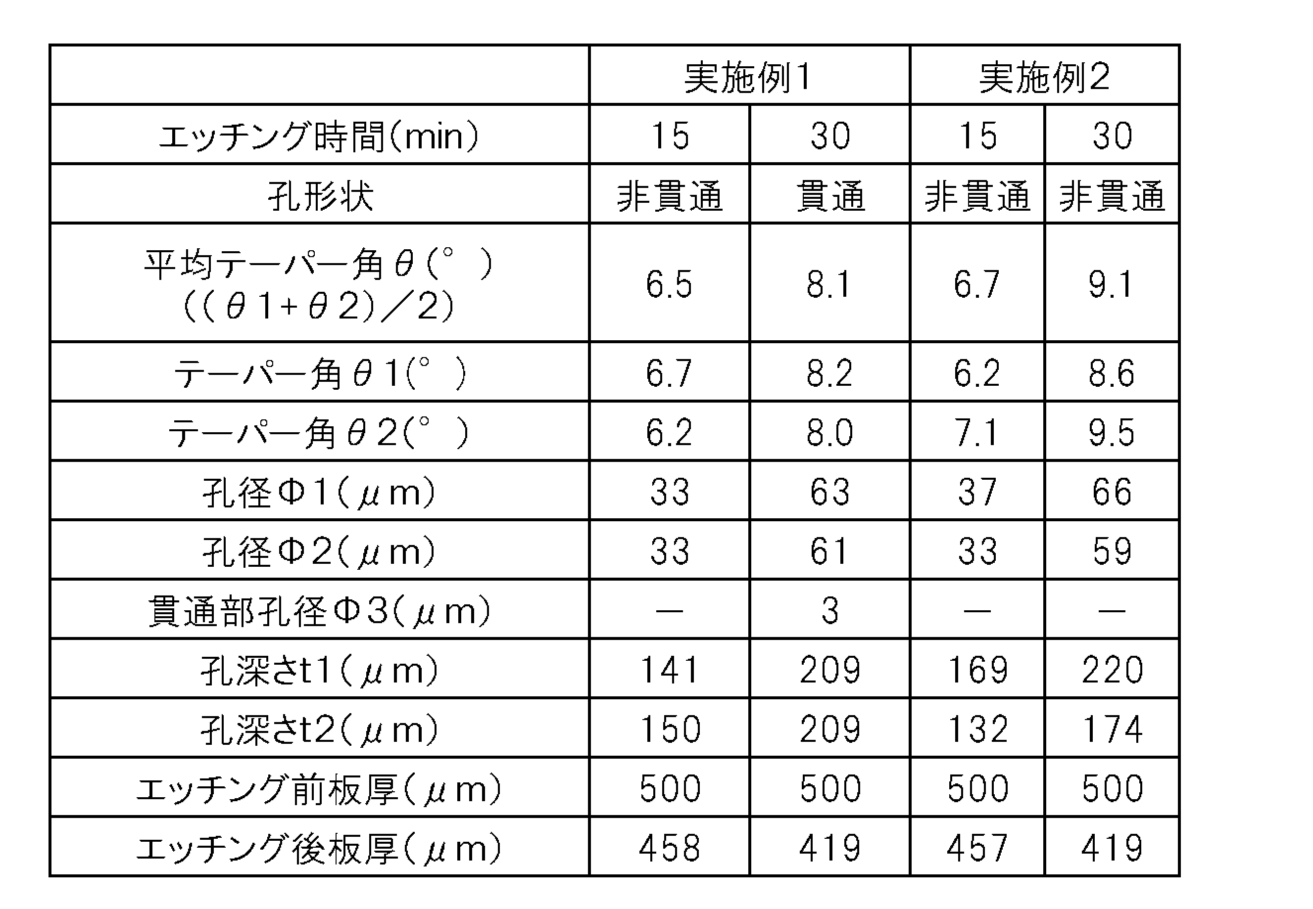
表1、2から、無アルカリガラス原板の仮想温度が低いと、熱処理後の無アルカリガラス原板のエッチングレートERaが低下し、ER/ERaの値が小さくなった。その結果、貫通孔の平均テーパー角θが小さくなった。また、エッチング時間が長い程、平均テーパー角θが大きくなった。
上記では、孔を形成していない無アルカリガラス原板について、ER/ERaの値を評価したが、貫通孔を形成した後の実施例1に係る無アルカリガラス基板(熱処理されていない貫通孔を有するガラス基板)について、ER/ERaの値を評価したところ、ERとERaの値が0.89であり、ER/ERaの値が1.00であった。また貫通孔を形成した後の実施例2に係る無アルカリガラス基板(熱処理されていない貫通孔を有するガラス基板)について、ER/ERaの値を評価したところ、ERの値が1.00、ERaの値が0.89であり、ER/ERaの値が1.12であった。
(実施例3)
まず、板厚500μmの無アルカリガラス原板(日本電気硝子社製商品名OA-11、徐冷点Ta743℃)を準備し、図6に示す温度プロファイルに沿って室温(25℃)からアニールし、この無アルカリガラス原板のHFエッチングレート(ER)を測定した。更に、この無アルカリガラス原板を図5に示す温度プロファイルに沿って室温(25℃)から熱処理し、HFエッチングレート(ERa)を測定した。また、このガラス原板(アニール済み、且つ熱処理をしていないもの)について、実施例1と同様の方法により孔の形成を行った。
まず、板厚500μmの無アルカリガラス原板(日本電気硝子社製商品名OA-11、徐冷点Ta743℃)を準備し、図6に示す温度プロファイルに沿って室温(25℃)からアニールし、この無アルカリガラス原板のHFエッチングレート(ER)を測定した。更に、この無アルカリガラス原板を図5に示す温度プロファイルに沿って室温(25℃)から熱処理し、HFエッチングレート(ERa)を測定した。また、このガラス原板(アニール済み、且つ熱処理をしていないもの)について、実施例1と同様の方法により孔の形成を行った。
(実施例4)
まず、板厚500μmの無アルカリガラス原板(日本電気硝子社製商品名OA-11、徐冷点Ta743℃)を準備し、図7に示す温度プロファイルに沿って室温(25℃)からアニールし、この無アルカリガラス原板のHFエッチングレート(ER)を測定した。更に、この無アルカリガラス原板を図5に示す温度プロファイルに沿って室温(25℃)から熱処理し、HFエッチングレート(ERa)を測定した。また、このガラス原板(アニール済み、且つ熱処理をしていないもの)について、実施例1と同様の方法により孔の形成を行った。
まず、板厚500μmの無アルカリガラス原板(日本電気硝子社製商品名OA-11、徐冷点Ta743℃)を準備し、図7に示す温度プロファイルに沿って室温(25℃)からアニールし、この無アルカリガラス原板のHFエッチングレート(ER)を測定した。更に、この無アルカリガラス原板を図5に示す温度プロファイルに沿って室温(25℃)から熱処理し、HFエッチングレート(ERa)を測定した。また、このガラス原板(アニール済み、且つ熱処理をしていないもの)について、実施例1と同様の方法により孔の形成を行った。
(実施例5)
まず、板厚500μmの無アルカリガラス原板(日本電気硝子社製商品名OA-11、徐冷点Ta743℃)を準備し、図8に示す温度プロファイルに沿って室温(25℃)からアニールし、この無アルカリガラス原板のHFエッチングレート(ER)を測定した。更に、この無アルカリガラス原板を図5に示す温度プロファイルに沿って室温(25℃)から熱処理し、HFエッチングレート(ERa)を測定した。また、このガラス原板(アニール済み、且つ熱処理をしていないもの)について、実施例1と同様の方法により孔の形成を行った。
まず、板厚500μmの無アルカリガラス原板(日本電気硝子社製商品名OA-11、徐冷点Ta743℃)を準備し、図8に示す温度プロファイルに沿って室温(25℃)からアニールし、この無アルカリガラス原板のHFエッチングレート(ER)を測定した。更に、この無アルカリガラス原板を図5に示す温度プロファイルに沿って室温(25℃)から熱処理し、HFエッチングレート(ERa)を測定した。また、このガラス原板(アニール済み、且つ熱処理をしていないもの)について、実施例1と同様の方法により孔の形成を行った。
表3に実施例3~5に係るガラス原板のHFエッチングレートを示し、更に実施例3~5に係るガラス基板の孔形状を示す。

表3によると、アニール時の冷却速度を遅くすると、ガラス原板(ガラス基板)の仮想温度が低くなり、ガラス原板のエッチングレートERが低下し、ER/ERaの値が小さくなった。その結果、孔の平均テーパー角θが小さくなった。
上記では、孔を形成していない無アルカリガラス原板について、ER/ERaの値を評価したが、貫通孔を形成した後の実施例3に係る無アルカリガラス基板(熱処理されていない貫通孔を有するガラス基板)について、ER/ERaの値を評価したところ、ERの値が0.93、ERaの値が0.89であり、ER/ERaの値が1.04であった。また、貫通孔を形成した後の実施例4に係る無アルカリガラス基板(熱処理されていない貫通孔を有するガラス基板)について、ER/ERaの値を評価したところ、ERの値が0.94、ERaの値が0.89であり、ER/ERaの値が1.06であった。更に、貫通孔を形成した後の実施例5に係る無アルカリガラス基板(熱処理されていない貫通孔を有するガラス基板)について、ER/ERaの値を評価したところ、ERの値が0.97、ERaの値が0.89であり、ER/ERaの値が1.09であった。
なお、実施例2~5において、ガラス原板に形成された孔は非貫通であったが、貫通孔を形成するためにエッチング時間を長くした場合であっても、ER/ERaの値を小さくすることにより、孔の平均テーパー角θを小さくし得ることが表1~3から読み取れる。表3によると、貫通孔を形成するためのガラス原板をアニールする際は、アニール時の冷却速度が遅いことが好ましい。この結果は、オフラインアニールを行わなくても、オーバーフローダウンドロー法による成形時において、通常よりも板引き速度を遅くすること等の成形条件の調整により、貫通孔のテーパー角を低減し得ることを示している。
100 ガラス基板(ガラス原板)
20 貫通孔
21 非貫通孔
101 第一面
100 第二面
20 貫通孔
21 非貫通孔
101 第一面
100 第二面
Claims (8)
- 貫通孔を有するガラス基板において、ガラス基板のHFエッチングレートをER、そのガラス基板を熱処理した後のHFエッチングレートをERaとした時に、ER/ERaの値が1.50以下になることを特徴とするガラス基板。
- ガラス基板の表面における貫通孔の孔直径が1μm~200μmであることを特徴とする請求項1に記載のガラス基板。
- 貫通孔の厚み方向の平均テーパー角θが0°~13°であることを特徴とする請求項1又は2に記載のガラス基板。
- 貫通孔を形成するための貫通孔形成用ガラス原板であって、ガラス原板のHFエッチングレートをER、そのガラス原板を熱処理した後のHFエッチングレートをERaとした時に、ER/ERaの値が1.50以下になることを特徴とする貫通孔形成用ガラス原板。
- 貫通孔を形成するための貫通孔形成用ガラス原板を用意する工程と、
ガラス原板に貫通孔を形成して、貫通孔を有するガラス基板を得る工程と、を備え、
ガラス基板のHFエッチングレートをER、そのガラス基板を熱処理した後のHFエッチングレートをERaとした時に、ER/ERaの値が1.50以下になることを特徴とするガラス基板の製造方法。 - 貫通孔を形成するための貫通孔形成用ガラス原板を用意する工程と、
ガラス原板に貫通孔を形成して、貫通孔を有するガラス基板を得る工程と、を備え、
ガラス原板のHFエッチングレートをER、そのガラス原板を熱処理した後のHFエッチングレートをERaとした時に、ER/ERaの値が1.50以下になることを特徴とするガラス基板の製造方法。 - 貫通孔の厚み方向の平均テーパー角θが0°~13°であることを特徴とする請求項5又は6に記載のガラス基板の製造方法。
- ガラス原板をアニールする工程を更に備えることを特徴とする請求項5~7の何れかに記載のガラス基板の製造方法。
Priority Applications (4)
| Application Number | Priority Date | Filing Date | Title |
|---|---|---|---|
| JP2023507040A JPWO2022196510A1 (ja) | 2021-03-15 | 2022-03-10 | |
| PCT/JP2022/010505 WO2022196510A1 (ja) | 2021-03-15 | 2022-03-10 | ガラス基板、貫通孔形成用ガラス原板及びガラス基板の製造方法 |
| KR1020237033099A KR20230157991A (ko) | 2021-03-15 | 2022-03-10 | 유리 기판, 관통 구멍 형성용 유리 원판 및 유리 기판의 제조 방법 |
| CN202280019824.6A CN116981645A (zh) | 2021-03-15 | 2022-03-10 | 玻璃基板、贯通孔形成用玻璃原板以及玻璃基板的制造方法 |
Applications Claiming Priority (2)
| Application Number | Priority Date | Filing Date | Title |
|---|---|---|---|
| JP2021-040949 | 2021-03-15 | ||
| JP2021040949 | 2021-03-15 |
Publications (1)
| Publication Number | Publication Date |
|---|---|
| WO2022196019A1 true WO2022196019A1 (ja) | 2022-09-22 |
Family
ID=83320094
Family Applications (2)
| Application Number | Title | Priority Date | Filing Date |
|---|---|---|---|
| PCT/JP2021/047908 Ceased WO2022196019A1 (ja) | 2021-03-15 | 2021-12-23 | ガラス基板、貫通孔形成用ガラス原板及びガラス基板の製造方法 |
| PCT/JP2022/010505 Ceased WO2022196510A1 (ja) | 2021-03-15 | 2022-03-10 | ガラス基板、貫通孔形成用ガラス原板及びガラス基板の製造方法 |
Family Applications After (1)
| Application Number | Title | Priority Date | Filing Date |
|---|---|---|---|
| PCT/JP2022/010505 Ceased WO2022196510A1 (ja) | 2021-03-15 | 2022-03-10 | ガラス基板、貫通孔形成用ガラス原板及びガラス基板の製造方法 |
Country Status (4)
| Country | Link |
|---|---|
| JP (1) | JPWO2022196510A1 (ja) |
| KR (1) | KR20230157991A (ja) |
| CN (1) | CN116981645A (ja) |
| WO (2) | WO2022196019A1 (ja) |
Cited By (1)
| Publication number | Priority date | Publication date | Assignee | Title |
|---|---|---|---|---|
| WO2025169876A1 (ja) * | 2024-02-08 | 2025-08-14 | 日本電気硝子株式会社 | 光接続部材、光接続構造体、ガラス基板並びに光接続部材及びガラス基板の製造方法 |
Families Citing this family (5)
| Publication number | Priority date | Publication date | Assignee | Title |
|---|---|---|---|---|
| JP7521565B2 (ja) * | 2022-09-30 | 2024-07-24 | Toppanホールディングス株式会社 | ガラス基板、多層配線基板、およびガラス基板の製造方法 |
| JP2024051691A (ja) * | 2022-09-30 | 2024-04-11 | Toppanホールディングス株式会社 | ガラス基板、多層配線基板、およびガラス基板の製造方法 |
| WO2024070319A1 (ja) * | 2022-09-30 | 2024-04-04 | Toppanホールディングス株式会社 | ガラス基板、多層配線基板、およびガラス基板の製造方法 |
| KR102708159B1 (ko) * | 2024-01-23 | 2024-09-20 | 주식회사 세원하이텍 | 폴더블 글래스 및 이를 제조하는 방법 |
| WO2025239285A1 (ja) * | 2024-05-14 | 2025-11-20 | Agc株式会社 | 絶縁基板、及び回路基板 |
Citations (4)
| Publication number | Priority date | Publication date | Assignee | Title |
|---|---|---|---|---|
| JP2013537723A (ja) * | 2010-08-26 | 2013-10-03 | コーニング インコーポレイテッド | ガラスインターポーザパネル及びその作製方法 |
| JP2019055888A (ja) * | 2017-09-20 | 2019-04-11 | 日本電気硝子株式会社 | レーザーアシストエッチング用ガラス基板、及びそれを用いた有孔ガラス基板の製造方法 |
| JP2019089082A (ja) * | 2017-11-13 | 2019-06-13 | ビアメカニクス株式会社 | レーザ加工方法 |
| JP2019530629A (ja) * | 2016-09-08 | 2019-10-24 | コーニング インコーポレイテッド | 形態的属性を備えた孔を有する物品及びその製作方法 |
Family Cites Families (14)
| Publication number | Priority date | Publication date | Assignee | Title |
|---|---|---|---|---|
| US5163220A (en) * | 1991-10-09 | 1992-11-17 | The Unites States Of America As Represented By The Secretary Of The Army | Method of enhancing the electrical conductivity of indium-tin-oxide electrode stripes |
| DE102006043738B4 (de) * | 2006-09-13 | 2008-10-16 | Heraeus Quarzglas Gmbh & Co. Kg | Bauteil aus Quarzglas zum Einsatz bei der Halbleiterfertigung und Verfahren zur Herstellung desselben |
| KR101479804B1 (ko) * | 2007-09-13 | 2015-01-06 | 아사히 가라스 가부시키가이샤 | TiO2 함유 석영 유리 기판 |
| GB201011582D0 (en) * | 2010-07-09 | 2010-08-25 | Heraeus Quartz Uk Ltd | High purity synthetic silica and items such as semiconductor jigs manufactured therefrom |
| KR102157750B1 (ko) | 2012-11-29 | 2020-09-21 | 코닝 인코포레이티드 | 레이저 손상 및 에칭에 의한 유리 제품의 제조방법 |
| JP2015146401A (ja) | 2014-02-04 | 2015-08-13 | 大日本印刷株式会社 | ガラスインターポーザー |
| JP6295897B2 (ja) | 2014-09-05 | 2018-03-20 | 旭硝子株式会社 | ガラス基板に貫通孔を形成する装置および方法 |
| JP6700201B2 (ja) | 2015-02-10 | 2020-05-27 | 日本板硝子株式会社 | レーザ加工用ガラス及びそれを用いた孔付きガラスの製造方法 |
| CN107250073B (zh) * | 2015-02-13 | 2020-10-30 | 日本板硝子株式会社 | 激光加工用玻璃及使用了其的带孔玻璃的制造方法 |
| JP5994954B1 (ja) | 2015-09-25 | 2016-09-21 | 旭硝子株式会社 | 貫通孔を有するガラス基板の製造方法、貫通電極を備えるガラス基板の製造方法、およびインターポーザの製造方法 |
| TWI785052B (zh) | 2017-06-01 | 2022-12-01 | 美商康寧公司 | 包括穿透孔洞貫孔的組件基板及其製作方法 |
| JP2019099414A (ja) * | 2017-12-01 | 2019-06-24 | クアーズテック株式会社 | シリカガラス部材及びシリカガラス部材の製造方法 |
| JP7139886B2 (ja) * | 2018-10-30 | 2022-09-21 | Agc株式会社 | 孔を有するガラス基板の製造方法、およびアニール用ガラス積層体 |
| JP2020097506A (ja) * | 2018-12-19 | 2020-06-25 | 日本電気硝子株式会社 | アルミノシリケートガラス |
-
2021
- 2021-12-23 WO PCT/JP2021/047908 patent/WO2022196019A1/ja not_active Ceased
-
2022
- 2022-03-10 KR KR1020237033099A patent/KR20230157991A/ko active Pending
- 2022-03-10 WO PCT/JP2022/010505 patent/WO2022196510A1/ja not_active Ceased
- 2022-03-10 CN CN202280019824.6A patent/CN116981645A/zh active Pending
- 2022-03-10 JP JP2023507040A patent/JPWO2022196510A1/ja active Pending
Patent Citations (4)
| Publication number | Priority date | Publication date | Assignee | Title |
|---|---|---|---|---|
| JP2013537723A (ja) * | 2010-08-26 | 2013-10-03 | コーニング インコーポレイテッド | ガラスインターポーザパネル及びその作製方法 |
| JP2019530629A (ja) * | 2016-09-08 | 2019-10-24 | コーニング インコーポレイテッド | 形態的属性を備えた孔を有する物品及びその製作方法 |
| JP2019055888A (ja) * | 2017-09-20 | 2019-04-11 | 日本電気硝子株式会社 | レーザーアシストエッチング用ガラス基板、及びそれを用いた有孔ガラス基板の製造方法 |
| JP2019089082A (ja) * | 2017-11-13 | 2019-06-13 | ビアメカニクス株式会社 | レーザ加工方法 |
Cited By (1)
| Publication number | Priority date | Publication date | Assignee | Title |
|---|---|---|---|---|
| WO2025169876A1 (ja) * | 2024-02-08 | 2025-08-14 | 日本電気硝子株式会社 | 光接続部材、光接続構造体、ガラス基板並びに光接続部材及びガラス基板の製造方法 |
Also Published As
| Publication number | Publication date |
|---|---|
| KR20230157991A (ko) | 2023-11-17 |
| CN116981645A (zh) | 2023-10-31 |
| JPWO2022196510A1 (ja) | 2022-09-22 |
| WO2022196510A1 (ja) | 2022-09-22 |
| TW202248155A (zh) | 2022-12-16 |
Similar Documents
| Publication | Publication Date | Title |
|---|---|---|
| WO2022196510A1 (ja) | ガラス基板、貫通孔形成用ガラス原板及びガラス基板の製造方法 | |
| CN107250073B (zh) | 激光加工用玻璃及使用了其的带孔玻璃的制造方法 | |
| TWI675019B (zh) | 玻璃基板 | |
| TWI412499B (zh) | Glass and glass plate manufacturing methods | |
| JP5233998B2 (ja) | ガラス板およびその製造方法ならびにtftパネルの製造方法 | |
| KR102291291B1 (ko) | 무알칼리 유리의 제조 방법 | |
| WO2022075068A1 (ja) | 貫通孔を有するガラス基板 | |
| KR20200003274A (ko) | 무알칼리 유리 및 이것을 사용한 무알칼리 유리판 | |
| JP2014073960A (ja) | カバーガラスの製造方法及びカバーガラス | |
| JP2026026351A (ja) | ガラス基板 | |
| US20260085000A1 (en) | Glass substrate | |
| TWI917579B (zh) | 玻璃基板、貫通孔形成用玻璃原板以及玻璃基板的製造方法 | |
| WO2026071122A1 (ja) | 有孔ガラス基板、ガラス基板、及び有孔ガラス基板の製造方法 | |
| TW202615368A (zh) | 有孔玻璃基板、玻璃基板、玻璃基板及有孔玻璃基板的製造方法 | |
| JP5804846B2 (ja) | カバーガラスの製造方法 | |
| WO2024219376A1 (ja) | ガラス板の製造方法 | |
| TW202608839A (zh) | 玻璃板及玻璃板之製造方法 | |
| WO2026023373A1 (ja) | ガラス板及びガラス板の製造方法 | |
| JP2016102059A (ja) | ガラス基板及びその製造方法 |
Legal Events
| Date | Code | Title | Description |
|---|---|---|---|
| 121 | Ep: the epo has been informed by wipo that ep was designated in this application |
Ref document number: 21931761 Country of ref document: EP Kind code of ref document: A1 |
|
| NENP | Non-entry into the national phase |
Ref country code: DE |
|
| 122 | Ep: pct application non-entry in european phase |
Ref document number: 21931761 Country of ref document: EP Kind code of ref document: A1 |
|
| NENP | Non-entry into the national phase |
Ref country code: JP |