WO2022157934A1 - 半導体装置および半導体装置の製造方法 - Google Patents
半導体装置および半導体装置の製造方法 Download PDFInfo
- Publication number
- WO2022157934A1 WO2022157934A1 PCT/JP2021/002281 JP2021002281W WO2022157934A1 WO 2022157934 A1 WO2022157934 A1 WO 2022157934A1 JP 2021002281 W JP2021002281 W JP 2021002281W WO 2022157934 A1 WO2022157934 A1 WO 2022157934A1
- Authority
- WO
- WIPO (PCT)
- Prior art keywords
- groove
- base plate
- semiconductor device
- warp
- convex
- Prior art date
- Legal status (The legal status is an assumption and is not a legal conclusion. Google has not performed a legal analysis and makes no representation as to the accuracy of the status listed.)
- Ceased
Links
Images












Classifications
-
- H—ELECTRICITY
- H10—SEMICONDUCTOR DEVICES; ELECTRIC SOLID-STATE DEVICES NOT OTHERWISE PROVIDED FOR
- H10W—GENERIC PACKAGES, INTERCONNECTIONS, CONNECTORS OR OTHER CONSTRUCTIONAL DETAILS OF DEVICES COVERED BY CLASS H10
- H10W70/00—Package substrates; Interposers; Redistribution layers [RDL]
- H10W70/60—Insulating or insulated package substrates; Interposers; Redistribution layers
- H10W70/67—Insulating or insulated package substrates; Interposers; Redistribution layers characterised by their insulating layers or insulating parts
- H10W70/68—Shapes or dispositions thereof
-
- H—ELECTRICITY
- H10—SEMICONDUCTOR DEVICES; ELECTRIC SOLID-STATE DEVICES NOT OTHERWISE PROVIDED FOR
- H10W—GENERIC PACKAGES, INTERCONNECTIONS, CONNECTORS OR OTHER CONSTRUCTIONAL DETAILS OF DEVICES COVERED BY CLASS H10
- H10W40/00—Arrangements for thermal protection or thermal control
- H10W40/40—Arrangements for thermal protection or thermal control involving heat exchange by flowing fluids
- H10W40/47—Arrangements for thermal protection or thermal control involving heat exchange by flowing fluids by flowing liquids, e.g. forced water cooling
-
- H—ELECTRICITY
- H10—SEMICONDUCTOR DEVICES; ELECTRIC SOLID-STATE DEVICES NOT OTHERWISE PROVIDED FOR
- H10W—GENERIC PACKAGES, INTERCONNECTIONS, CONNECTORS OR OTHER CONSTRUCTIONAL DETAILS OF DEVICES COVERED BY CLASS H10
- H10W40/00—Arrangements for thermal protection or thermal control
- H10W40/60—Securing means for detachable heating or cooling arrangements, e.g. clamps
- H10W40/611—Bolts or screws
-
- H—ELECTRICITY
- H10—SEMICONDUCTOR DEVICES; ELECTRIC SOLID-STATE DEVICES NOT OTHERWISE PROVIDED FOR
- H10W—GENERIC PACKAGES, INTERCONNECTIONS, CONNECTORS OR OTHER CONSTRUCTIONAL DETAILS OF DEVICES COVERED BY CLASS H10
- H10W90/00—Package configurations
Definitions
- the present disclosure relates to a semiconductor device and a method for manufacturing a semiconductor device.
- Patent Literature 1 discloses a semiconductor device comprising a semiconductor chip, an insulating substrate having a main surface to which the semiconductor chip is bonded, and a base having a main surface to which the other main surface of the insulating substrate is bonded.
- a convex portion is provided on the other main surface of the base, and an annular groove is provided on the outer periphery of the convex portion.
- a seal made of an annular elastic body is inserted along the groove.
- a case having an opening is arranged so that the outer edge of the opening is in contact with the sealing material.
- a sealing material is sandwiched between a base plate and a cooler to secure a sufficient crushing amount to prevent leakage of cooling water.
- the crushing amount of the sealing material is obtained by applying a load to the sealing material.
- the load is not applied uniformly over the entire circumference of the sealing material, there is a risk that the compression amount will vary and the cooling water will leak.
- the member will crack due to compression.
- the clearance between the base plate and the cooler may not be uniform, and the crushing amount of the sealing material may vary.
- An object of the present disclosure is to obtain a semiconductor device and a method for manufacturing a semiconductor device that can suppress variations in the amount of crushing of the sealing material.
- a semiconductor device includes a base plate having a top surface and a back surface opposite to the top surface, and an annular groove formed in the back surface; a substrate provided on the top surface of the base plate; a semiconductor chip provided on the upper surface of the substrate, the base plate having a convex warped portion that is convex to the upper surface side, and the convex warped portion formed in the groove The portion becomes deeper as it moves away from the maximum warp portion having the largest warp among the convex warp portions.
- a semiconductor device includes a base plate having a top surface and a back surface on the opposite side of the top surface and having an annular groove formed in the back surface; a substrate provided on the top surface of the base plate; a semiconductor chip provided on the upper surface of the substrate, the base plate having a concave warped portion that is convex to the back surface side, and the groove is formed in the concave warped portion
- the part has a constant depth.
- a semiconductor device includes a base plate having a top surface and a back surface opposite to the top surface, and having an annular groove formed in the back surface; a substrate provided on the top surface of the base plate; A semiconductor chip provided on the upper surface of the substrate, a sealing material accommodated in the groove, and a cooler fixed to the back surface of the base plate so as to cover the groove, the base plate comprising: It has a stress generating portion in which stress is generated in a direction that warps the base plate so as to be convex on the back surface side, and the portion of the groove formed in the stress generating portion has a constant depth. .
- a substrate is mounted on the top surface of a base plate having a top surface and a back surface opposite to the top surface, and an annular groove is formed in the back surface.
- a semiconductor chip is mounted on the upper surface, the base plate has a concave warped portion that is convex to the back side, and the base covers the groove in a state in which the sealing material is accommodated in the groove.
- a cooler is fixed to the back surface of the plate to reduce warping of the concave warp, and the portion of the groove formed in the concave warp has a constant depth.
- the depth of the groove is set according to the direction of warpage of the base plate. For this reason, it is possible to suppress variations in the crushing amount of the sealing material.
- FIG. 1 is a cross-sectional view of a semiconductor device according to a first embodiment
- FIG. 4 is a bottom view of the base plate according to Embodiment 1
- FIG. FIG. 4 is a cross-sectional view of the base plate according to Embodiment 1 in a state in which no warpage occurs
- FIG. 4 is a cross-sectional view of the base plate according to Embodiment 1 in a state in which warpage has occurred
- FIG. 4 is a cross-sectional view of a state in which the base plate according to Embodiment 1 is attached to the cooler
- FIG. 11 is a cross-sectional view of a state in which the base plate according to Embodiment 2 is not warped
- FIG. 11 is a cross-sectional view of a state in which the base plate according to the second embodiment is warped;
- FIG. 8 is a cross-sectional view of a state in which a base plate according to Embodiment 2 is attached to a cooler;
- FIG. 11 is a cross-sectional view of a state in which a base plate according to Embodiment 3 is not warped;
- FIG. 12 is a cross-sectional view of a state in which the base plate according to Embodiment 3 is warped;
- FIG. 11 is a cross-sectional view of a state in which a base plate according to Embodiment 4 is not warped;
- FIG. 11 is a cross-sectional view of a state in which a base plate according to Embodiment 4 is warped;
- FIG. 11 is a cross-sectional view of a state in which a base plate according to Embodiment 5 is not warped;
- FIG. 14 is a cross-sectional view of a state in which the base plate according to Embodiment 5 is warped;
- FIG. 11 is a cross-sectional view of a state in which a base plate according to Embodiment 6 is not warped;
- FIG. 14 is a cross-sectional view of a state in which the base plate according to Embodiment 6 is warped;
- FIG. 11 is a cross-sectional view of a state in which the base plate according to Embodiment 4 is warped;
- FIG. 11 is a cross-sectional view of a state in which a base plate according to Embodiment 5 is not warped;
- FIG. 14 is a cross-sectional view of a state in
- FIG. 11 is a cross-sectional view of a state in which a base plate according to Embodiment 6 is attached to a cooler;
- FIG. 21 is a cross-sectional view of a state in which a base plate according to Embodiment 7 is not warped;
- FIG. 14 is a cross-sectional view of a state in which a base plate according to Embodiment 7 is warped;
- FIG. 21 is a cross-sectional view of a state in which a base plate according to Embodiment 8 is not warped;
- FIG. 21 is a cross-sectional view of a state in which a base plate according to Embodiment 8 is warped;
- FIG. 21 is a cross-sectional view of a state in which a base plate according to Embodiment 8 is warped;
- FIG. 21 is a cross-sectional view of a state in which the base plate according to the ninth embodiment is not warped;
- FIG. 22 is another cross-sectional view of the base plate according to the ninth embodiment in a state in which warp is not generated;
- FIG. 21 is a cross-sectional view of a state in which the base plate according to the ninth embodiment is warped;
- FIG. 21 is another cross-sectional view of a state in which the base plate according to the ninth embodiment is warped;
- FIG. 21 is a cross-sectional view of a state in which a base plate according to Embodiment 9 is attached to a cooler;
- FIG. 21 is another cross-sectional view of a state in which the base plate according to the ninth embodiment is attached to the cooler;
- FIG. 1 is a cross-sectional view of a semiconductor device 100 according to Embodiment 1.
- FIG. A semiconductor device 100 includes a base plate 1 , a substrate 2 provided on the upper surface of the base plate 1 , and a semiconductor chip 3 provided on the upper surface of the substrate 2 .
- FIG. 2 is a bottom view of the base plate 1 according to Embodiment 1.
- the base plate 1 has a top surface and a back surface opposite to the top surface, and an annular groove 5 is formed in the back surface.
- the groove 5 is quadrangular in plan view.
- the seal material 4 is accommodated in the groove 5.
- a cooler 7 is fixed to the back surface of the base plate 1 .
- the outer edge of cooler 7 covers groove 5 .
- Cooler 7 holds cooling water 6 .
- the base plate 1 is fastened to the cooler 7 by fastening members 8 .
- the cooling water 6 can be sealed by fixing the base plate 1 to the cooler 7 via the sealing material 4 .
- the semiconductor chip 3 is, for example, a power semiconductor chip.
- the semiconductor chip 3 is, for example, an IGBT (Insulated Gate Bipolar Transistor), a MOSFET (Metal-Oxide-Semiconductor Field-Effect Transistor), or a diode.
- a power semiconductor chip may become hot during operation, and it is important to ensure high heat dissipation.
- the semiconductor chip 3 is made of Si, for example.
- the semiconductor chip 3 may be made of a wide bandgap semiconductor. Wide bandgap semiconductors are, for example, silicon carbide, gallium nitride based materials or diamond. If the semiconductor chip 3 is made of a wide bandgap semiconductor, it can operate at high temperatures. Therefore, it is important to ensure particularly high heat dissipation. Although two semiconductor chips 3 are shown in FIG. 1, the number of semiconductor chips 3 included in the semiconductor device 100 may be one or more.
- the substrate 2 is, for example, an insulating substrate.
- the substrate 2 comprises a surface circuit pattern 2a, a ceramic substrate 2b and a back circuit pattern 2c.
- the ceramic substrate 2b is made of ceramic such as Al2O3, AlN, Si3N4.
- the surface circuit pattern 2a and the back circuit pattern 2c are formed of metal containing Cu as a main component, for example.
- the surface circuit pattern 2a and the back circuit pattern 2c are formed on the upper surface and the back surface of the ceramic substrate 2b, respectively.
- the surface circuit pattern 2a is selectively formed on the upper surface of the ceramic substrate 2b. Thus, a circuit is formed on the upper surface of the ceramic substrate 2b.
- the back surface electrode of at least one semiconductor chip 3 is joined to the upper surface of the surface circuit pattern 2a.
- the back electrode is, for example, a collector electrode.
- the semiconductor chip 3 is connected to the surface circuit pattern 2a via a bonding material.
- the bonding material is, for example, lead-free solder such as Sn—Ag.
- Various wirings are formed on the surface electrodes of the semiconductor chip 3 by bonding wires, metal plates, or the like.
- the surface electrodes are for example emitter electrodes or gate electrodes. With the configuration described above, circuits necessary for the semiconductor device 100 are formed. Moreover, the periphery of the semiconductor chip 3 is protected by an outer frame, lid, sealing resin, etc. (not shown).
- the base plate 1 is plate-shaped.
- Base plate 1 is made of a metal material such as copper or a copper alloy.
- the back circuit pattern 2c of the substrate 2 is bonded to the base plate 1 via a bonding material.
- the bonding material is, for example, lead-free solder such as Sn—Ag.
- the cooler 7 is box-shaped and has an opening. Cooler 7 has a function of supplying cooling water 6 to semiconductor device 100 and holding it.
- the cooler 7 is made of a metal material such as Al or an Al alloy. Thereby, the durability of the cooler 7 holding the cooling water 6 can be ensured.
- the cooler 7 also has a supply port and a discharge port (not shown) for circulating the cooling water 6 to and from the external radiator.
- the sealing material 4 is an annular elastic body made of, for example, a rubber material.
- the sealing material 4 is, for example, an O-ring. Between the base plate 1 and the cooler 7, the sealing material 4 is inserted into the groove 5 and arranged. Through holes 9 are formed in the four corners of the base plate 1 outside the grooves 5 . A fastening member 8 such as a bolt is inserted into the through hole 9 . As a result, the base plate 1 is held while being pressed against the cooler 7 . At this time, the sealing material 4 adheres to the portion of the base plate 1 where the groove 5 is formed and the cooler 7 while exerting an elastic force. Thereby, the entire gap between the base plate 1 and the cooler 7 can be filled with the sealing material 4 . Therefore, leakage of the cooling water 6 to the outside can be prevented. Such a cooling method is also called direct cooling.
- FIG. 3 is a cross-sectional view of the base plate 1a according to Embodiment 1 in a state in which no warpage occurs.
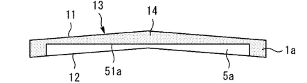
- FIG. 4 is a cross-sectional view showing a state in which the base plate 1a according to Embodiment 1 is warped. 3 and 4 show cross sections of the base plate 1a along one of the four sides of the groove 5a. The depth of the groove 5a in the base plate 1a increases as the distance from the center of one side of the groove 5a increases.
- the depth of the grooves 5a is non-uniform in the state shown in FIG.
- the base plate 1a warps so as to protrude toward the upper surface 11 due to heat load or the like during assembly. That is, the base plate 1a has a convex warped portion 13 that is convex toward the upper surface 11 side.
- the portion of the groove 5a formed in the convex warp portion 13 becomes deeper as the distance from the maximum warp portion 14 of the convex warp portion 13 with the largest warp increases.
- the depth of the groove 5a is the height from the back surface 12 of the base plate 1a to the bottom 51a of the groove 5a.
- maximum warp portion 14 is a portion where the upper surface 11 of the base plate 1a protrudes most.
- Maximum warp portion 14 in the present embodiment is formed at the center of one side of groove 5a. In the portion of the groove 5a formed in the convex warp portion 13, the thickness between the bottom portion 51a of the groove 5a and the upper surface 11 of the base plate 1a becomes smaller as the distance from the maximum warp portion 14 increases.
- FIG. 5 is a cross-sectional view of the state where the base plate 1a according to Embodiment 1 is attached to the cooler 7.
- FIG. 5 By warping the base plate 1a so as to project toward the upper surface 11, the difference in depth of the grooves 5a is canceled. That is, the height from the cooler 7 to the bottom 51a of the groove 5a can be made uniform. Therefore, variations in the amount of compression of the seal material 4 can be suppressed.
- the base plate 1a is fixed to the cooler 7 at its end. Therefore, when the base plate 1a is fixed to the cooler 7, the force for correcting the warp is difficult to act. Therefore, even when the base plate 1a shown in FIG. 5 is attached to the cooler 7, the shape of the groove 5a shown in FIG. 4 can be maintained. Therefore, variations in the amount of compression of the seal material 4 can be suppressed. As a result, leakage of cooling water 6 and compression cracking of members can be suppressed.
- the depth of the groove is increased as it approaches the edge of the base plate without considering the warped shape of the base plate.
- compression cracks may occur in the member at portions where the amount of crushing is excessive.
- the depth of groove 5 is set according to the warp direction of base plate 1 . Therefore, variations in the crushing amount of the sealing material 4 can be reliably suppressed.
- the bottom portion 51a of the portion of the groove 5a formed in the convex warp portion 13 is formed flat.
- the sealing material 4 can be evenly flattened.
- the bottom 51a of the groove 5a in the warped state can be composed of one plane. Thereby, the sealing material 4 can be crushed more uniformly.
- the bottom 51a of the groove 5a in the warped state may not be one plane, and the height from the cooler 7 to the bottom 51a of the groove 5a may not be completely uniform.
- the height from the cooler 7 to the bottom 51a of the groove 5a may vary depending on the position as long as leakage of cooling water can be prevented.
- the structure shown in FIGS. 4 and 5 should be formed on at least one of the four sides of the groove 5a. That is, at least one side of the groove 5a formed in the convex warp portion 13 should be deeper as the distance from the maximum warp portion 14 increases. Moreover, the groove 5a may be polygonal, elliptical, or circular in plan view.
- the method of fixing the base plate 1 and the cooler 7 is not limited to fastening with bolts.
- the base plate 1 and cooler 7 may be fitted together.
- the base plate 1 may be fixed while being pressed against the cooler 7 .
- a semiconductor device and a method of manufacturing a semiconductor device according to the following embodiments have many points in common with the first embodiment, and thus differences from the first embodiment will be mainly described.
- FIG. 6 is a cross-sectional view showing a state in which the base plate 1b according to the second embodiment is not warped.
- FIG. 7 is a cross-sectional view of a state in which the base plate 1b according to Embodiment 2 is warped.
- the present embodiment differs from the first embodiment in the structure and warp direction of the base plate 1b. The depth of the groove 5b of the base plate 1b in this embodiment is constant.
- the depth of the groove 5b is uniform in the state shown in FIG. 6 in which no warp occurs before assembly.
- the base plate 1b warps so as to protrude toward the rear surface 12 due to the heat load and the like during assembly. That is, the base plate 1b has a concave warped portion 15 that is convex toward the back surface 12 side. A portion of the groove 5b formed in the concave warp portion 15 has a constant depth.
- the semiconductor chip 3 is mounted on the top surface of the substrate 2 .
- the substrate 2 is mounted on the upper surface of the base plate 1b.
- the cooler 7 is fixed to the back surface 12 of the base plate 1b so as to cover the groove 5b.
- the warp of the concave warp portion 15 is reduced compared to before it is fixed to the cooler 7 .
- the assembly order of the substrate 2, the semiconductor chip 3, the base plate 1b, the sealing material 4, and the cooler 7 may be changed.
- FIG. 8 is a cross-sectional view of a state in which the base plate 1b according to Embodiment 2 is attached to the cooler 7.
- FIG. The base plate 1b is fixed to the cooler 7 at its end. Therefore, when the base plate 1b is fixed to the cooler 7, a force for correcting the warp is likely to act. Therefore, when the base plate 1b shown in FIG. 8 is attached to the cooler 7, the grooves 5b have substantially the same shape as the state shown in FIG. 6 where there is no warp. Therefore, the height from the cooler 7 to the bottom portion 51b of the groove 5b can be made uniform, and variations in the crushing amount of the sealing material 4 can be suppressed.
- a stress is generated in the base plate 1b in a direction that warps the base plate 1b so as to project toward the rear surface 12 side. That is, the base plate 1b has the stress-generating portion 16 in which stress is generated in a direction that warps the base plate 1b so as to protrude toward the back surface 12 side.
- the portion of the groove 5b formed in the stress generating portion 16 has a constant depth.
- the bottom 51b of the groove 5b in this embodiment is flat. Not limited to this, the bottom 51b of the groove 5b may be curved or may have unevenness. Moreover, in the state where the base plate 1b is attached to the cooler 7, the height from the cooler 7 to the bottom 51b of the groove 5b may not be completely uniform.
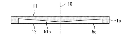
- FIG. 9 is a cross-sectional view showing a state in which the base plate 1c according to Embodiment 3 is not warped.
- FIG. 10 is a cross-sectional view of a state in which the base plate 1c according to Embodiment 3 is warped.
- the base plate 1 c has a convex warp portion 13 .
- the groove 5c of the base plate 1c is polygonal in plan view. Further, as in the first embodiment, at least one side of the groove 5c formed in the convex warp portion 13 becomes deeper as it approaches the end of the one side.
- the depth of the groove 5c is symmetrical with respect to the center 10 of the one side.
- the angle .theta.1 indicating the amount of change in the depth of the groove 5c is the same.
- the angle ⁇ 1 is the angle formed by the back surface 12 of the base plate 1c and the bottom portion 51c of the groove 5c in a cross-sectional view.
- the sealing material 4 can be reliably crushed at the center 10 of the side of the groove 5c where the base plate 1c is likely to become the maximum warp portion 14 when assembled to the cooler 7.
- FIG. 11 is a cross-sectional view of the base plate 1d according to the fourth embodiment in which no warpage occurs.
- FIG. 12 is a cross-sectional view showing a state in which the base plate 1d according to the fourth embodiment is warped.
- This embodiment differs from the third embodiment in the shape of the groove 5d of the base plate 1d.
- a portion of the groove 5b formed in the convex warp portion 13 becomes deeper as the distance from the center 10 increases.
- the depth of the groove 5d is symmetrical with respect to the center 10.
- a bottom portion 51d of the portion of the groove 5d formed in the convex warp portion 13 is formed with a curved surface.
- the shape of the bottom portion 51d is the same on both sides of the center 10. As shown in FIG.
- the height from the cooler 7 to the bottom 51d of the groove 5d is not completely uniform.
- the difference in the depth of the grooves 5d is canceled by the base plate 1d being warped so as to protrude toward the upper surface 11 side. Therefore, variations in the amount of compression of the seal material 4 can be suppressed.
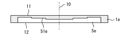
- FIG. 13 is a cross-sectional view showing a state in which the base plate 1e according to Embodiment 5 is not warped.
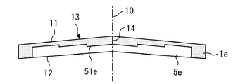
- FIG. 14 is a cross-sectional view of a state in which the base plate 1e according to the fifth embodiment is warped.
- This embodiment differs from the third embodiment in the shape of the groove 5e of the base plate 1e.
- a portion of the groove 5e formed in the convex warp portion 13 becomes deeper as the distance from the center 10 increases.
- the depth of the groove 5e is symmetrical with respect to the center 10.
- FIG. A bottom portion 51e of the portion of the groove 5e formed in the convex warp portion 13 has a stepped shape.
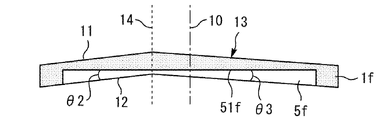
- FIG. 15 is a cross-sectional view of the base plate 1f according to the sixth embodiment in which no warpage occurs.
- FIG. 16 is a cross-sectional view of a state in which the base plate 1f according to Embodiment 6 is warped.
- FIG. 17 is a cross-sectional view of a state in which the base plate 1f according to Embodiment 6 is attached to the cooler 7.
- FIG. This embodiment differs from the first embodiment in the shape of the groove 5f of the base plate 1f.
- the base plate 1 f has a convex warp portion 13 .
- the groove 5f of the base plate 1f is polygonal in plan view. A portion of the groove 5f formed in the convex warp portion 13 becomes deeper as the distance from the maximum warp portion 14 increases.
- the bottom portion 51f of the groove 5f is formed from a flat surface.
- the maximum warp portion 14 is provided at a position displaced from the center 10 of one side of the groove 5f formed in the convex warp portion 13 in the direction along the side.
- the side where the distance from the maximum warp 14 to the end of the one side is short is the side where the distance from the maximum warp 14 to the end of the one side is long.
- the depth of the groove 5f changes greatly when the maximum warp portion 14 is separated from the maximum warp portion 14 by a certain distance. That is, ⁇ 2> ⁇ 3.
- the depth of the groove 5f is equal at both ends of one side of the groove 5f formed in the convex warp portion 13. As shown in FIG.
- the depth of the groove 5f is made uniform as shown in FIG. be able to. Therefore, variations in the amount of compression of the seal material 4 can be suppressed.
- FIG. 18 is a cross-sectional view of the base plate 1g according to Embodiment 7 in a state in which no warpage occurs.
- FIG. 19 is a cross-sectional view showing a state in which the base plate 1g according to Embodiment 7 is warped.
- the shape of the groove 5g of the base plate 1g differs from that of the sixth embodiment.
- a bottom portion 51g of the groove 5g is formed from a curved surface.
- the maximum warp portion 14 of the base plate 1g is provided at a position shifted in the direction along the side from the center 10 of the side formed in the convex warp portion 13 of the groove 5g.
- the side where the distance from the maximum warp portion 14 to the end of the one side is short is the side where the distance from the maximum warp portion 14 to the end of the one side is long.
- the depth of the groove 5g changes greatly when the maximum warp portion 14 is separated from the maximum warp portion 14 by a certain distance. That is, the side where the distance from the maximum warp portion 14 to the end of the side of the groove 5g is short has a larger curvature than the side where the distance from the maximum warp 14 to the end of the side of the groove 5g is long.
- the sealing material 4 can be reliably crushed at the maximum warp portion 14.
- FIG. 20 is a cross-sectional view showing a state in which the base plate 1h according to the eighth embodiment is not warped.
- FIG. 21 is a cross-sectional view showing a state in which the base plate 1h according to the eighth embodiment is warped. This embodiment differs from the sixth embodiment in the shape of the groove 5h of the base plate 1h. A bottom portion 51h of the groove 5h is stepped.
- the maximum warp portion 14 of the base plate 1h is provided at a position shifted in the direction along the side from the center 10 of the side formed in the convex warp portion 13 of the groove 5h.
- the side where the distance from the maximum warp portion 14 to the end of the one side is short is the side where the distance from the maximum warp portion 14 to the end of the one side is long.
- the depth of the groove 5h changes greatly when the maximum warp portion 14 is separated from the maximum warp portion 14 by a certain distance.
- the sealing material 4 can be reliably crushed at the maximum warp portion 14.
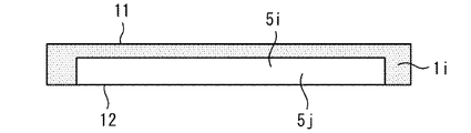
- FIG. 22 is a cross-sectional view showing a state in which the base plate 1i according to the ninth embodiment is not warped.
- FIG. 23 is another cross-sectional view of the base plate 1i according to the ninth embodiment in which no warpage occurs.
- This embodiment differs from the first embodiment in the shape of the groove 5i of the base plate 1i.
- a groove 5j and a groove 5k shown in FIGS. 22 and 23 constitute one side of the groove 5i of the present embodiment.
- the groove 5j has a constant depth.
- the groove 5k becomes deeper as it moves away from the center of the groove 5k in the longitudinal direction of the groove 5k.
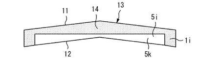
- FIG. 24 is a cross-sectional view of a state in which the base plate 1i according to the ninth embodiment is warped.
- FIG. 25 is another cross-sectional view of a state in which the base plate 1i according to the ninth embodiment is warped.
- a groove 5j having a constant depth is formed in the concave warp portion 15 of the base plate 1i.
- the groove 5 k is formed in the convex warp portion 13 .
- the groove 5k becomes deeper as the distance from the maximum warp portion 14 increases.
- the base plate 1i has both the convex warp portion 13 and the concave warp portion 15.
- the groove 5j has the same depth as both ends of the deepest groove 5k.
- FIG. 26 is a cross-sectional view of a state where the base plate 1i according to the ninth embodiment is attached to the cooler 7.
- FIG. The base plate 1i is fixed with the cooler 7 at its end.
- a force for correcting the warp is likely to act on the concave warp portion 15 . Therefore, in the state shown in FIG. 26, the groove 5j has substantially the same shape as the state shown in FIG. 22 in which no warpage occurs. Therefore, the height from the cooler 7 to the bottom of the groove 5j can be made uniform, and variation in the crushing amount of the sealing material 4 can be suppressed.
- stress is generated in the portion of the base plate 1i where the groove 5j is formed in a direction that warps the base plate 1i so as to project toward the back surface 12 side.
- the groove 5j is formed in a stress-generating portion 16 where stress is generated in a direction that warps the base plate 1i so as to protrude toward the rear surface 12 of the base plate 1i.
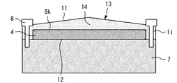
- FIG. 27 is another cross-sectional view of the state where the base plate 1i according to the ninth embodiment is attached to the cooler 7.
- FIG. 27 When the base plate 1 i is fixed to the cooler 7 , a force for correcting the warp is less likely to act on the convex warped portion 13 . Therefore, even in the state shown in FIG. 27, the shape of the groove 5k shown in FIG. 25 can be maintained. Therefore, the height from the cooler 7 to the bottom of the groove 5k can be made uniform, and variation in the crushing amount of the sealing material 4 can be suppressed.
- the height from the cooler 7 to the bottom of the groove 5i can be made uniform even in a structure in which different warped shapes are mixed. Therefore, it is possible to suppress variations in the amount of crushing over the entire circumference of the sealing material 4 .
- 1, 1a-1i base plate, 2: substrate, 2a: surface circuit pattern, 2b: ceramic substrate, 2c: back circuit pattern, 3: semiconductor chip, 4: sealing material, 5, 5a-5k: groove, 6: cooling water, 7: cooler, 8: fastening member, 9 through hole, 10 center, 11 upper surface, 12 back surface, 13 convex warp, 14 maximum warp, 15 concave warp, 16 stress generating part, 51a-51h bottom, 100 semiconductor device
Landscapes
- Cooling Or The Like Of Semiconductors Or Solid State Devices (AREA)
- Engineering & Computer Science (AREA)
- Manufacturing & Machinery (AREA)
- Dicing (AREA)
Priority Applications (5)
| Application Number | Priority Date | Filing Date | Title |
|---|---|---|---|
| JP2022576907A JP7476987B2 (ja) | 2021-01-22 | 2021-01-22 | 半導体装置および半導体装置の製造方法 |
| DE112021006881.4T DE112021006881T5 (de) | 2021-01-22 | 2021-01-22 | Halbleitervorrichtung und Verfahren zur Herstellung einer Halbleitervorrichtung |
| CN202180090933.2A CN116711072A (zh) | 2021-01-22 | 2021-01-22 | 半导体装置及半导体装置的制造方法 |
| US18/043,828 US12424500B2 (en) | 2021-01-22 | 2021-01-22 | Semiconductor device and method for manufacturing semiconductor device |
| PCT/JP2021/002281 WO2022157934A1 (ja) | 2021-01-22 | 2021-01-22 | 半導体装置および半導体装置の製造方法 |
Applications Claiming Priority (1)
| Application Number | Priority Date | Filing Date | Title |
|---|---|---|---|
| PCT/JP2021/002281 WO2022157934A1 (ja) | 2021-01-22 | 2021-01-22 | 半導体装置および半導体装置の製造方法 |
Publications (1)
| Publication Number | Publication Date |
|---|---|
| WO2022157934A1 true WO2022157934A1 (ja) | 2022-07-28 |
Family
ID=82549616
Family Applications (1)
| Application Number | Title | Priority Date | Filing Date |
|---|---|---|---|
| PCT/JP2021/002281 Ceased WO2022157934A1 (ja) | 2021-01-22 | 2021-01-22 | 半導体装置および半導体装置の製造方法 |
Country Status (5)
| Country | Link |
|---|---|
| US (1) | US12424500B2 (https=) |
| JP (1) | JP7476987B2 (https=) |
| CN (1) | CN116711072A (https=) |
| DE (1) | DE112021006881T5 (https=) |
| WO (1) | WO2022157934A1 (https=) |
Families Citing this family (2)
| Publication number | Priority date | Publication date | Assignee | Title |
|---|---|---|---|---|
| CN116711072A (zh) * | 2021-01-22 | 2023-09-05 | 三菱电机株式会社 | 半导体装置及半导体装置的制造方法 |
| WO2023058597A1 (ja) * | 2021-10-06 | 2023-04-13 | デンカ株式会社 | 放熱部材 |
Citations (4)
| Publication number | Priority date | Publication date | Assignee | Title |
|---|---|---|---|---|
| JP2005033140A (ja) * | 2003-07-11 | 2005-02-03 | Nissan Motor Co Ltd | 半導体装置 |
| JP2010192708A (ja) * | 2009-02-18 | 2010-09-02 | Hitachi Ltd | 半導体パワーモジュール、電力変換装置、および、半導体パワーモジュールの製造方法 |
| JP2015073012A (ja) * | 2013-10-03 | 2015-04-16 | 富士電機株式会社 | 半導体装置 |
| JP2017126681A (ja) * | 2016-01-15 | 2017-07-20 | カルソニックカンセイ株式会社 | 半導体ユニット |
Family Cites Families (18)
| Publication number | Priority date | Publication date | Assignee | Title |
|---|---|---|---|---|
| JPS51112279A (en) | 1975-03-28 | 1976-10-04 | Hitachi Ltd | Semiconductor device |
| JP3346657B2 (ja) | 1994-09-09 | 2002-11-18 | 京セラ株式会社 | 半導体素子収納用パッケージ |
| US7117930B2 (en) * | 2002-06-14 | 2006-10-10 | Thermal Corp. | Heat pipe fin stack with extruded base |
| JP4806803B2 (ja) * | 2003-10-21 | 2011-11-02 | Dowaメタルテック株式会社 | 金属−セラミックス接合基板およびその製造方法 |
| KR101077378B1 (ko) * | 2010-06-23 | 2011-10-26 | 삼성전기주식회사 | 방열기판 및 그 제조방법 |
| US8872332B2 (en) * | 2012-04-30 | 2014-10-28 | Infineon Technologies Ag | Power module with directly attached thermally conductive structures |
| DE112015000253B4 (de) * | 2014-07-18 | 2023-06-29 | Fuji Electric Co., Ltd. | Halbleitervorrichtung |
| JP6406121B2 (ja) * | 2015-05-14 | 2018-10-17 | 三菱電機株式会社 | 高周波高出力デバイス |
| JP6526323B2 (ja) * | 2016-04-04 | 2019-06-05 | 三菱電機株式会社 | パワーモジュール、パワー半導体装置及びパワーモジュール製造方法 |
| DE112017002999B4 (de) * | 2016-06-16 | 2022-03-24 | Mitsubishi Electric Corporation | Halbleiter-montage-wärmeabführungs-basisplatte und herstellungsverfahren für dieselbe |
| WO2018131583A1 (ja) * | 2017-01-13 | 2018-07-19 | 三菱電機株式会社 | 金属-セラミックス接合基板及びその製造方法 |
| JP6769541B2 (ja) * | 2017-02-23 | 2020-10-14 | 三菱電機株式会社 | 半導体装置 |
| US11227808B2 (en) * | 2017-09-05 | 2022-01-18 | Mitsubishi Electric Corporation | Power module and method for fabricating the same, and power conversion device |
| JP2019096797A (ja) * | 2017-11-27 | 2019-06-20 | 三菱電機株式会社 | 半導体装置および電力変換装置 |
| JP7070661B2 (ja) * | 2018-03-20 | 2022-05-18 | 富士電機株式会社 | 半導体装置 |
| WO2021106114A1 (ja) * | 2019-11-27 | 2021-06-03 | 三菱電機株式会社 | 半導体モジュール |
| CN116711072A (zh) * | 2021-01-22 | 2023-09-05 | 三菱电机株式会社 | 半导体装置及半导体装置的制造方法 |
| JP7482815B2 (ja) * | 2021-03-09 | 2024-05-14 | 三菱電機株式会社 | 半導体装置および半導体装置の製造方法 |
-
2021
- 2021-01-22 CN CN202180090933.2A patent/CN116711072A/zh active Pending
- 2021-01-22 WO PCT/JP2021/002281 patent/WO2022157934A1/ja not_active Ceased
- 2021-01-22 US US18/043,828 patent/US12424500B2/en active Active
- 2021-01-22 JP JP2022576907A patent/JP7476987B2/ja active Active
- 2021-01-22 DE DE112021006881.4T patent/DE112021006881T5/de active Pending
Patent Citations (4)
| Publication number | Priority date | Publication date | Assignee | Title |
|---|---|---|---|---|
| JP2005033140A (ja) * | 2003-07-11 | 2005-02-03 | Nissan Motor Co Ltd | 半導体装置 |
| JP2010192708A (ja) * | 2009-02-18 | 2010-09-02 | Hitachi Ltd | 半導体パワーモジュール、電力変換装置、および、半導体パワーモジュールの製造方法 |
| JP2015073012A (ja) * | 2013-10-03 | 2015-04-16 | 富士電機株式会社 | 半導体装置 |
| JP2017126681A (ja) * | 2016-01-15 | 2017-07-20 | カルソニックカンセイ株式会社 | 半導体ユニット |
Also Published As
| Publication number | Publication date |
|---|---|
| CN116711072A (zh) | 2023-09-05 |
| US20230352354A1 (en) | 2023-11-02 |
| JP7476987B2 (ja) | 2024-05-01 |
| US12424500B2 (en) | 2025-09-23 |
| JPWO2022157934A1 (https=) | 2022-07-28 |
| DE112021006881T5 (de) | 2023-11-09 |
Similar Documents
| Publication | Publication Date | Title |
|---|---|---|
| JP5900620B2 (ja) | 半導体装置 | |
| JP5738226B2 (ja) | 電力用半導体装置モジュール | |
| JP6323325B2 (ja) | 半導体装置、半導体装置の製造方法 | |
| US20080203559A1 (en) | Power device package and semiconductor package mold for fabricating the same | |
| WO2017175612A1 (ja) | パワーモジュール、パワー半導体装置及びパワーモジュール製造方法 | |
| JP2015073012A (ja) | 半導体装置 | |
| JP6699742B2 (ja) | 半導体装置 | |
| US11232991B2 (en) | Semiconductor apparatus | |
| JP2014216459A (ja) | 半導体装置 | |
| KR20070090555A (ko) | 전력 소자용 패키지 및 패키지 어셈블리 | |
| CN107924893A (zh) | 功率模块、功率模块的散热构造、以及功率模块的接合方法 | |
| JP7476987B2 (ja) | 半導体装置および半導体装置の製造方法 | |
| JP7187814B2 (ja) | 半導体装置 | |
| US20180025993A1 (en) | Semiconductor device | |
| US12033916B2 (en) | Semiconductor device and semiconductor module with improved heat dissipation | |
| JP6946698B2 (ja) | 半導体装置および半導体装置の製造方法 | |
| US11456275B2 (en) | Semiconductor device and method of manufacturing semiconductor device | |
| KR102815718B1 (ko) | 전력소자 | |
| JP2019047094A (ja) | 半導体装置 | |
| US20230215776A1 (en) | Semiconductor device | |
| JP7180385B2 (ja) | 半導体装置 | |
| US20220285254A1 (en) | Semiconductor device and method for manufacturing semiconductor device | |
| JP2019009280A (ja) | 半導体装置 | |
| JP7136367B2 (ja) | 半導体パッケージ | |
| JP7601261B2 (ja) | 半導体装置及びその製造方法 |
Legal Events
| Date | Code | Title | Description |
|---|---|---|---|
| 121 | Ep: the epo has been informed by wipo that ep was designated in this application |
Ref document number: 21921043 Country of ref document: EP Kind code of ref document: A1 |
|
| ENP | Entry into the national phase |
Ref document number: 2022576907 Country of ref document: JP Kind code of ref document: A |
|
| WWE | Wipo information: entry into national phase |
Ref document number: 202180090933.2 Country of ref document: CN |
|
| WWE | Wipo information: entry into national phase |
Ref document number: 112021006881 Country of ref document: DE |
|
| 122 | Ep: pct application non-entry in european phase |
Ref document number: 21921043 Country of ref document: EP Kind code of ref document: A1 |
|
| WWG | Wipo information: grant in national office |
Ref document number: 18043828 Country of ref document: US |