WO2022130803A1 - Carte de câblage - Google Patents
Carte de câblage Download PDFInfo
- Publication number
- WO2022130803A1 WO2022130803A1 PCT/JP2021/040014 JP2021040014W WO2022130803A1 WO 2022130803 A1 WO2022130803 A1 WO 2022130803A1 JP 2021040014 W JP2021040014 W JP 2021040014W WO 2022130803 A1 WO2022130803 A1 WO 2022130803A1
- Authority
- WO
- WIPO (PCT)
- Prior art keywords
- wiring electrode
- opaque
- protective layer
- transparent protective
- substrate
- Prior art date
Links
- 239000000758 substrate Substances 0.000 claims abstract description 161
- 239000011241 protective layer Substances 0.000 claims abstract description 121
- 239000010410 layer Substances 0.000 claims description 79
- 239000000049 pigment Substances 0.000 claims description 33
- 239000011342 resin composition Substances 0.000 claims description 19
- 238000013508 migration Methods 0.000 claims description 18
- 230000005012 migration Effects 0.000 claims description 18
- 239000012790 adhesive layer Substances 0.000 claims description 12
- 238000002310 reflectometry Methods 0.000 abstract 1
- 239000010408 film Substances 0.000 description 57
- 230000015572 biosynthetic process Effects 0.000 description 55
- 238000000034 method Methods 0.000 description 46
- 238000004519 manufacturing process Methods 0.000 description 35
- 238000011156 evaluation Methods 0.000 description 28
- 239000000203 mixture Substances 0.000 description 28
- 229920005989 resin Polymers 0.000 description 27
- 239000011347 resin Substances 0.000 description 27
- NIXOWILDQLNWCW-UHFFFAOYSA-M Acrylate Chemical compound [O-]C(=O)C=C NIXOWILDQLNWCW-UHFFFAOYSA-M 0.000 description 24
- 239000000178 monomer Substances 0.000 description 21
- 238000010586 diagram Methods 0.000 description 18
- 150000002500 ions Chemical class 0.000 description 17
- 238000000576 coating method Methods 0.000 description 16
- 239000000975 dye Substances 0.000 description 16
- 239000011248 coating agent Substances 0.000 description 15
- 230000003287 optical effect Effects 0.000 description 14
- 229920006243 acrylic copolymer Polymers 0.000 description 13
- 125000003178 carboxy group Chemical group [H]OC(*)=O 0.000 description 13
- 239000002245 particle Substances 0.000 description 13
- 230000000052 comparative effect Effects 0.000 description 12
- -1 polyethylene terephthalate Polymers 0.000 description 12
- 239000000243 solution Substances 0.000 description 12
- 238000006243 chemical reaction Methods 0.000 description 11
- 238000001035 drying Methods 0.000 description 11
- PPBRXRYQALVLMV-UHFFFAOYSA-N Styrene Chemical compound C=CC1=CC=CC=C1 PPBRXRYQALVLMV-UHFFFAOYSA-N 0.000 description 10
- 239000002313 adhesive film Substances 0.000 description 10
- 239000003999 initiator Substances 0.000 description 10
- OKKJLVBELUTLKV-UHFFFAOYSA-N Methanol Chemical compound OC OKKJLVBELUTLKV-UHFFFAOYSA-N 0.000 description 9
- 239000007864 aqueous solution Substances 0.000 description 9
- 229920001971 elastomer Polymers 0.000 description 9
- 239000000463 material Substances 0.000 description 9
- 238000002360 preparation method Methods 0.000 description 9
- LLHKCFNBLRBOGN-UHFFFAOYSA-N propylene glycol methyl ether acetate Chemical compound COCC(C)OC(C)=O LLHKCFNBLRBOGN-UHFFFAOYSA-N 0.000 description 9
- 239000005060 rubber Substances 0.000 description 9
- LFQSCWFLJHTTHZ-UHFFFAOYSA-N Ethanol Chemical compound CCO LFQSCWFLJHTTHZ-UHFFFAOYSA-N 0.000 description 8
- KFZMGEQAYNKOFK-UHFFFAOYSA-N Isopropanol Chemical compound CC(C)O KFZMGEQAYNKOFK-UHFFFAOYSA-N 0.000 description 8
- VYPSYNLAJGMNEJ-UHFFFAOYSA-N Silicium dioxide Chemical compound O=[Si]=O VYPSYNLAJGMNEJ-UHFFFAOYSA-N 0.000 description 8
- 125000002887 hydroxy group Chemical group [H]O* 0.000 description 8
- 238000000206 photolithography Methods 0.000 description 8
- WGTYBPLFGIVFAS-UHFFFAOYSA-M tetramethylammonium hydroxide Chemical compound [OH-].C[N+](C)(C)C WGTYBPLFGIVFAS-UHFFFAOYSA-M 0.000 description 8
- 238000002834 transmittance Methods 0.000 description 8
- XLYOFNOQVPJJNP-UHFFFAOYSA-N water Substances O XLYOFNOQVPJJNP-UHFFFAOYSA-N 0.000 description 8
- ZMANZCXQSJIPKH-UHFFFAOYSA-N Triethylamine Chemical compound CCN(CC)CC ZMANZCXQSJIPKH-UHFFFAOYSA-N 0.000 description 7
- QTBSBXVTEAMEQO-UHFFFAOYSA-N acetic acid Substances CC(O)=O QTBSBXVTEAMEQO-UHFFFAOYSA-N 0.000 description 7
- 239000000853 adhesive Substances 0.000 description 7
- 230000001070 adhesive effect Effects 0.000 description 7
- 239000011521 glass Substances 0.000 description 7
- 239000002932 luster Substances 0.000 description 7
- 229910052751 metal Inorganic materials 0.000 description 7
- 239000002184 metal Substances 0.000 description 7
- 229920002799 BoPET Polymers 0.000 description 6
- VEXZGXHMUGYJMC-UHFFFAOYSA-N Hydrochloric acid Chemical compound Cl VEXZGXHMUGYJMC-UHFFFAOYSA-N 0.000 description 6
- ZMXDDKWLCZADIW-UHFFFAOYSA-N N,N-Dimethylformamide Chemical compound CN(C)C=O ZMXDDKWLCZADIW-UHFFFAOYSA-N 0.000 description 6
- KDLHZDBZIXYQEI-UHFFFAOYSA-N Palladium Chemical compound [Pd] KDLHZDBZIXYQEI-UHFFFAOYSA-N 0.000 description 6
- MCMNRKCIXSYSNV-UHFFFAOYSA-N Zirconium dioxide Chemical compound O=[Zr]=O MCMNRKCIXSYSNV-UHFFFAOYSA-N 0.000 description 6
- NIXOWILDQLNWCW-UHFFFAOYSA-N acrylic acid group Chemical group C(C=C)(=O)O NIXOWILDQLNWCW-UHFFFAOYSA-N 0.000 description 6
- 238000011161 development Methods 0.000 description 6
- 238000010438 heat treatment Methods 0.000 description 6
- 229920001296 polysiloxane Polymers 0.000 description 6
- 239000003795 chemical substances by application Substances 0.000 description 5
- 150000002923 oximes Chemical class 0.000 description 5
- 238000006116 polymerization reaction Methods 0.000 description 5
- 239000004094 surface-active agent Substances 0.000 description 5
- VVBLNCFGVYUYGU-UHFFFAOYSA-N 4,4'-Bis(dimethylamino)benzophenone Chemical compound C1=CC(N(C)C)=CC=C1C(=O)C1=CC=C(N(C)C)C=C1 VVBLNCFGVYUYGU-UHFFFAOYSA-N 0.000 description 4
- IAZDPXIOMUYVGZ-UHFFFAOYSA-N Dimethylsulphoxide Chemical compound CS(C)=O IAZDPXIOMUYVGZ-UHFFFAOYSA-N 0.000 description 4
- SECXISVLQFMRJM-UHFFFAOYSA-N N-Methylpyrrolidone Chemical compound CN1CCCC1=O SECXISVLQFMRJM-UHFFFAOYSA-N 0.000 description 4
- UEEJHVSXFDXPFK-UHFFFAOYSA-N N-dimethylaminoethanol Chemical compound CN(C)CCO UEEJHVSXFDXPFK-UHFFFAOYSA-N 0.000 description 4
- PXHVJJICTQNCMI-UHFFFAOYSA-N Nickel Chemical compound [Ni] PXHVJJICTQNCMI-UHFFFAOYSA-N 0.000 description 4
- ISWSIDIOOBJBQZ-UHFFFAOYSA-N Phenol Chemical compound OC1=CC=CC=C1 ISWSIDIOOBJBQZ-UHFFFAOYSA-N 0.000 description 4
- BQCADISMDOOEFD-UHFFFAOYSA-N Silver Chemical compound [Ag] BQCADISMDOOEFD-UHFFFAOYSA-N 0.000 description 4
- CDBYLPFSWZWCQE-UHFFFAOYSA-L Sodium Carbonate Chemical compound [Na+].[Na+].[O-]C([O-])=O CDBYLPFSWZWCQE-UHFFFAOYSA-L 0.000 description 4
- 239000006229 carbon black Substances 0.000 description 4
- 150000001875 compounds Chemical class 0.000 description 4
- 229920001577 copolymer Polymers 0.000 description 4
- JHIVVAPYMSGYDF-UHFFFAOYSA-N cyclohexanone Chemical compound O=C1CCCCC1 JHIVVAPYMSGYDF-UHFFFAOYSA-N 0.000 description 4
- 125000004386 diacrylate group Chemical group 0.000 description 4
- 239000002270 dispersing agent Substances 0.000 description 4
- 239000003822 epoxy resin Substances 0.000 description 4
- LZCLXQDLBQLTDK-UHFFFAOYSA-N ethyl 2-hydroxypropanoate Chemical compound CCOC(=O)C(C)O LZCLXQDLBQLTDK-UHFFFAOYSA-N 0.000 description 4
- VOZRXNHHFUQHIL-UHFFFAOYSA-N glycidyl methacrylate Chemical compound CC(=C)C(=O)OCC1CO1 VOZRXNHHFUQHIL-UHFFFAOYSA-N 0.000 description 4
- 229920000647 polyepoxide Polymers 0.000 description 4
- 235000012239 silicon dioxide Nutrition 0.000 description 4
- 229910052709 silver Inorganic materials 0.000 description 4
- 239000004332 silver Substances 0.000 description 4
- 239000000126 substance Substances 0.000 description 4
- NLHHRLWOUZZQLW-UHFFFAOYSA-N Acrylonitrile Chemical compound C=CC#N NLHHRLWOUZZQLW-UHFFFAOYSA-N 0.000 description 3
- RYGMFSIKBFXOCR-UHFFFAOYSA-N Copper Chemical compound [Cu] RYGMFSIKBFXOCR-UHFFFAOYSA-N 0.000 description 3
- KWYUFKZDYYNOTN-UHFFFAOYSA-M Potassium hydroxide Chemical compound [OH-].[K+] KWYUFKZDYYNOTN-UHFFFAOYSA-M 0.000 description 3
- HEMHJVSKTPXQMS-UHFFFAOYSA-M Sodium hydroxide Chemical compound [OH-].[Na+] HEMHJVSKTPXQMS-UHFFFAOYSA-M 0.000 description 3
- RTAQQCXQSZGOHL-UHFFFAOYSA-N Titanium Chemical compound [Ti] RTAQQCXQSZGOHL-UHFFFAOYSA-N 0.000 description 3
- 229910045601 alloy Inorganic materials 0.000 description 3
- 239000000956 alloy Substances 0.000 description 3
- ISAOCJYIOMOJEB-UHFFFAOYSA-N benzoin Chemical compound C=1C=CC=CC=1C(O)C(=O)C1=CC=CC=C1 ISAOCJYIOMOJEB-UHFFFAOYSA-N 0.000 description 3
- 229910052802 copper Inorganic materials 0.000 description 3
- 239000010949 copper Substances 0.000 description 3
- 238000001723 curing Methods 0.000 description 3
- 239000012972 dimethylethanolamine Substances 0.000 description 3
- 239000003112 inhibitor Substances 0.000 description 3
- 239000001023 inorganic pigment Substances 0.000 description 3
- 238000005259 measurement Methods 0.000 description 3
- 229910052757 nitrogen Inorganic materials 0.000 description 3
- 229920003986 novolac Polymers 0.000 description 3
- 229910052763 palladium Inorganic materials 0.000 description 3
- 238000007747 plating Methods 0.000 description 3
- 239000002798 polar solvent Substances 0.000 description 3
- 229920000642 polymer Polymers 0.000 description 3
- 238000007650 screen-printing Methods 0.000 description 3
- 239000000377 silicon dioxide Substances 0.000 description 3
- 239000002904 solvent Substances 0.000 description 3
- 238000005507 spraying Methods 0.000 description 3
- 229910052714 tellurium Inorganic materials 0.000 description 3
- PORWMNRCUJJQNO-UHFFFAOYSA-N tellurium atom Chemical compound [Te] PORWMNRCUJJQNO-UHFFFAOYSA-N 0.000 description 3
- 229920001187 thermosetting polymer Polymers 0.000 description 3
- RMVRSNDYEFQCLF-UHFFFAOYSA-N thiophenol Chemical compound SC1=CC=CC=C1 RMVRSNDYEFQCLF-UHFFFAOYSA-N 0.000 description 3
- 239000010936 titanium Substances 0.000 description 3
- 229910052719 titanium Inorganic materials 0.000 description 3
- RYHBNJHYFVUHQT-UHFFFAOYSA-N 1,4-Dioxane Chemical compound C1COCCO1 RYHBNJHYFVUHQT-UHFFFAOYSA-N 0.000 description 2
- OZAIFHULBGXAKX-UHFFFAOYSA-N 2-(2-cyanopropan-2-yldiazenyl)-2-methylpropanenitrile Chemical compound N#CC(C)(C)N=NC(C)(C)C#N OZAIFHULBGXAKX-UHFFFAOYSA-N 0.000 description 2
- SMZOUWXMTYCWNB-UHFFFAOYSA-N 2-(2-methoxy-5-methylphenyl)ethanamine Chemical compound COC1=CC=C(C)C=C1CCN SMZOUWXMTYCWNB-UHFFFAOYSA-N 0.000 description 2
- LEJBBGNFPAFPKQ-UHFFFAOYSA-N 2-(2-prop-2-enoyloxyethoxy)ethyl prop-2-enoate Chemical compound C=CC(=O)OCCOCCOC(=O)C=C LEJBBGNFPAFPKQ-UHFFFAOYSA-N 0.000 description 2
- HZAXFHJVJLSVMW-UHFFFAOYSA-N 2-Aminoethan-1-ol Chemical compound NCCO HZAXFHJVJLSVMW-UHFFFAOYSA-N 0.000 description 2
- INQDDHNZXOAFFD-UHFFFAOYSA-N 2-[2-(2-prop-2-enoyloxyethoxy)ethoxy]ethyl prop-2-enoate Chemical compound C=CC(=O)OCCOCCOCCOC(=O)C=C INQDDHNZXOAFFD-UHFFFAOYSA-N 0.000 description 2
- RZVINYQDSSQUKO-UHFFFAOYSA-N 2-phenoxyethyl prop-2-enoate Chemical compound C=CC(=O)OCCOC1=CC=CC=C1 RZVINYQDSSQUKO-UHFFFAOYSA-N 0.000 description 2
- KUDUQBURMYMBIJ-UHFFFAOYSA-N 2-prop-2-enoyloxyethyl prop-2-enoate Chemical compound C=CC(=O)OCCOC(=O)C=C KUDUQBURMYMBIJ-UHFFFAOYSA-N 0.000 description 2
- YEJRWHAVMIAJKC-UHFFFAOYSA-N 4-Butyrolactone Chemical compound O=C1CCCO1 YEJRWHAVMIAJKC-UHFFFAOYSA-N 0.000 description 2
- FUGYGGDSWSUORM-UHFFFAOYSA-N 4-hydroxystyrene Chemical compound OC1=CC=C(C=C)C=C1 FUGYGGDSWSUORM-UHFFFAOYSA-N 0.000 description 2
- 239000004925 Acrylic resin Substances 0.000 description 2
- 229920000178 Acrylic resin Polymers 0.000 description 2
- 241000009355 Antron Species 0.000 description 2
- IJGRMHOSHXDMSA-UHFFFAOYSA-N Atomic nitrogen Chemical compound N#N IJGRMHOSHXDMSA-UHFFFAOYSA-N 0.000 description 2
- 229930185605 Bisphenol Natural products 0.000 description 2
- OKTJSMMVPCPJKN-UHFFFAOYSA-N Carbon Chemical compound [C] OKTJSMMVPCPJKN-UHFFFAOYSA-N 0.000 description 2
- VYZAMTAEIAYCRO-UHFFFAOYSA-N Chromium Chemical compound [Cr] VYZAMTAEIAYCRO-UHFFFAOYSA-N 0.000 description 2
- ROSDSFDQCJNGOL-UHFFFAOYSA-N Dimethylamine Chemical compound CNC ROSDSFDQCJNGOL-UHFFFAOYSA-N 0.000 description 2
- GUUVPOWQJOLRAS-UHFFFAOYSA-N Diphenyl disulfide Chemical compound C=1C=CC=CC=1SSC1=CC=CC=C1 GUUVPOWQJOLRAS-UHFFFAOYSA-N 0.000 description 2
- VZCYOOQTPOCHFL-OWOJBTEDSA-N Fumaric acid Chemical compound OC(=O)\C=C\C(O)=O VZCYOOQTPOCHFL-OWOJBTEDSA-N 0.000 description 2
- PEDCQBHIVMGVHV-UHFFFAOYSA-N Glycerine Chemical compound OCC(O)CO PEDCQBHIVMGVHV-UHFFFAOYSA-N 0.000 description 2
- UQSXHKLRYXJYBZ-UHFFFAOYSA-N Iron oxide Chemical compound [Fe]=O UQSXHKLRYXJYBZ-UHFFFAOYSA-N 0.000 description 2
- BAPJBEWLBFYGME-UHFFFAOYSA-N Methyl acrylate Chemical compound COC(=O)C=C BAPJBEWLBFYGME-UHFFFAOYSA-N 0.000 description 2
- BAVYZALUXZFZLV-UHFFFAOYSA-N Methylamine Chemical compound NC BAVYZALUXZFZLV-UHFFFAOYSA-N 0.000 description 2
- FXHOOIRPVKKKFG-UHFFFAOYSA-N N,N-Dimethylacetamide Chemical compound CN(C)C(C)=O FXHOOIRPVKKKFG-UHFFFAOYSA-N 0.000 description 2
- 206010034972 Photosensitivity reaction Diseases 0.000 description 2
- 239000002202 Polyethylene glycol Substances 0.000 description 2
- 239000004820 Pressure-sensitive adhesive Substances 0.000 description 2
- XUIMIQQOPSSXEZ-UHFFFAOYSA-N Silicon Chemical compound [Si] XUIMIQQOPSSXEZ-UHFFFAOYSA-N 0.000 description 2
- 244000028419 Styrax benzoin Species 0.000 description 2
- 235000000126 Styrax benzoin Nutrition 0.000 description 2
- 235000008411 Sumatra benzointree Nutrition 0.000 description 2
- 150000001298 alcohols Chemical class 0.000 description 2
- PYKYMHQGRFAEBM-UHFFFAOYSA-N anthraquinone Natural products CCC(=O)c1c(O)c2C(=O)C3C(C=CC=C3O)C(=O)c2cc1CC(=O)OC PYKYMHQGRFAEBM-UHFFFAOYSA-N 0.000 description 2
- 150000004056 anthraquinones Chemical class 0.000 description 2
- 238000005452 bending Methods 0.000 description 2
- 229960002130 benzoin Drugs 0.000 description 2
- IISBACLAFKSPIT-UHFFFAOYSA-N bisphenol A Chemical compound C=1C=C(O)C=CC=1C(C)(C)C1=CC=C(O)C=C1 IISBACLAFKSPIT-UHFFFAOYSA-N 0.000 description 2
- 229910052804 chromium Inorganic materials 0.000 description 2
- 239000011651 chromium Substances 0.000 description 2
- 238000007334 copolymerization reaction Methods 0.000 description 2
- ZYGHJZDHTFUPRJ-UHFFFAOYSA-N coumarin Chemical compound C1=CC=C2OC(=O)C=CC2=C1 ZYGHJZDHTFUPRJ-UHFFFAOYSA-N 0.000 description 2
- PAFZNILMFXTMIY-UHFFFAOYSA-N cyclohexylamine Chemical compound NC1CCCCC1 PAFZNILMFXTMIY-UHFFFAOYSA-N 0.000 description 2
- BGTOWKSIORTVQH-UHFFFAOYSA-N cyclopentanone Chemical compound O=C1CCCC1 BGTOWKSIORTVQH-UHFFFAOYSA-N 0.000 description 2
- DMBHHRLKUKUOEG-UHFFFAOYSA-N diphenylamine Chemical compound C=1C=CC=CC=1NC1=CC=CC=C1 DMBHHRLKUKUOEG-UHFFFAOYSA-N 0.000 description 2
- 239000006185 dispersion Substances 0.000 description 2
- 238000005516 engineering process Methods 0.000 description 2
- 150000002148 esters Chemical class 0.000 description 2
- 229940116333 ethyl lactate Drugs 0.000 description 2
- 239000010419 fine particle Substances 0.000 description 2
- YLQWCDOCJODRMT-UHFFFAOYSA-N fluoren-9-one Chemical compound C1=CC=C2C(=O)C3=CC=CC=C3C2=C1 YLQWCDOCJODRMT-UHFFFAOYSA-N 0.000 description 2
- PCHJSUWPFVWCPO-UHFFFAOYSA-N gold Chemical compound [Au] PCHJSUWPFVWCPO-UHFFFAOYSA-N 0.000 description 2
- 229910052737 gold Inorganic materials 0.000 description 2
- 239000010931 gold Substances 0.000 description 2
- 238000007646 gravure printing Methods 0.000 description 2
- 235000019382 gum benzoic Nutrition 0.000 description 2
- 150000004820 halides Chemical class 0.000 description 2
- NAQMVNRVTILPCV-UHFFFAOYSA-N hexane-1,6-diamine Chemical compound NCCCCCCN NAQMVNRVTILPCV-UHFFFAOYSA-N 0.000 description 2
- 239000011133 lead Substances 0.000 description 2
- 239000002905 metal composite material Substances 0.000 description 2
- 239000007769 metal material Substances 0.000 description 2
- 229910052759 nickel Inorganic materials 0.000 description 2
- 239000012860 organic pigment Substances 0.000 description 2
- 125000002080 perylenyl group Chemical group C1(=CC=C2C=CC=C3C4=CC=CC5=CC=CC(C1=C23)=C45)* 0.000 description 2
- CSHWQDPOILHKBI-UHFFFAOYSA-N peryrene Natural products C1=CC(C2=CC=CC=3C2=C2C=CC=3)=C3C2=CC=CC3=C1 CSHWQDPOILHKBI-UHFFFAOYSA-N 0.000 description 2
- 230000036211 photosensitivity Effects 0.000 description 2
- IEQIEDJGQAUEQZ-UHFFFAOYSA-N phthalocyanine Chemical compound N1C(N=C2C3=CC=CC=C3C(N=C3C4=CC=CC=C4C(=N4)N3)=N2)=C(C=CC=C2)C2=C1N=C1C2=CC=CC=C2C4=N1 IEQIEDJGQAUEQZ-UHFFFAOYSA-N 0.000 description 2
- BASFCYQUMIYNBI-UHFFFAOYSA-N platinum Chemical compound [Pt] BASFCYQUMIYNBI-UHFFFAOYSA-N 0.000 description 2
- 229920001223 polyethylene glycol Polymers 0.000 description 2
- 229920001721 polyimide Polymers 0.000 description 2
- BWHMMNNQKKPAPP-UHFFFAOYSA-L potassium carbonate Chemical compound [K+].[K+].[O-]C([O-])=O BWHMMNNQKKPAPP-UHFFFAOYSA-L 0.000 description 2
- 239000002244 precipitate Substances 0.000 description 2
- 239000000047 product Substances 0.000 description 2
- 239000012487 rinsing solution Substances 0.000 description 2
- 230000035945 sensitivity Effects 0.000 description 2
- 229910052710 silicon Inorganic materials 0.000 description 2
- 239000010703 silicon Substances 0.000 description 2
- 229920002050 silicone resin Polymers 0.000 description 2
- 238000004528 spin coating Methods 0.000 description 2
- 238000004544 sputter deposition Methods 0.000 description 2
- LAJZODKXOMJMPK-UHFFFAOYSA-N tellurium dioxide Chemical compound O=[Te]=O LAJZODKXOMJMPK-UHFFFAOYSA-N 0.000 description 2
- HJUGFYREWKUQJT-UHFFFAOYSA-N tetrabromomethane Chemical compound BrC(Br)(Br)Br HJUGFYREWKUQJT-UHFFFAOYSA-N 0.000 description 2
- 229920002803 thermoplastic polyurethane Polymers 0.000 description 2
- 239000010409 thin film Substances 0.000 description 2
- VZCYOOQTPOCHFL-UHFFFAOYSA-N trans-butenedioic acid Natural products OC(=O)C=CC(O)=O VZCYOOQTPOCHFL-UHFFFAOYSA-N 0.000 description 2
- 230000007704 transition Effects 0.000 description 2
- RIOQSEWOXXDEQQ-UHFFFAOYSA-N triphenylphosphine Chemical compound C1=CC=CC=C1P(C=1C=CC=CC=1)C1=CC=CC=C1 RIOQSEWOXXDEQQ-UHFFFAOYSA-N 0.000 description 2
- 229910021642 ultra pure water Inorganic materials 0.000 description 2
- 239000012498 ultrapure water Substances 0.000 description 2
- 238000000870 ultraviolet spectroscopy Methods 0.000 description 2
- 238000001291 vacuum drying Methods 0.000 description 2
- 230000000007 visual effect Effects 0.000 description 2
- FYXIUZQDZQBKCN-UHFFFAOYSA-N (3-hydroxy-2,2,4-trimethylpentyl) prop-2-enoate Chemical compound CC(C)C(O)C(C)(C)COC(=O)C=C FYXIUZQDZQBKCN-UHFFFAOYSA-N 0.000 description 1
- LGPAKRMZNPYPMG-UHFFFAOYSA-N (3-hydroxy-2-prop-2-enoyloxypropyl) prop-2-enoate Chemical compound C=CC(=O)OC(CO)COC(=O)C=C LGPAKRMZNPYPMG-UHFFFAOYSA-N 0.000 description 1
- JTXDFCUHUYEYQE-UHFFFAOYSA-N 1,1-bis(sulfanylidene)-1,3-thiazole Chemical compound S=S1(=S)C=CN=C1 JTXDFCUHUYEYQE-UHFFFAOYSA-N 0.000 description 1
- SCEFCWXRXJZWHE-UHFFFAOYSA-N 1,2,3-tribromo-4-(2,3,4-tribromophenyl)sulfonylbenzene Chemical compound BrC1=C(Br)C(Br)=CC=C1S(=O)(=O)C1=CC=C(Br)C(Br)=C1Br SCEFCWXRXJZWHE-UHFFFAOYSA-N 0.000 description 1
- LRMDXTVKVHKWEK-UHFFFAOYSA-N 1,2-diaminoanthracene-9,10-dione Chemical compound C1=CC=C2C(=O)C3=C(N)C(N)=CC=C3C(=O)C2=C1 LRMDXTVKVHKWEK-UHFFFAOYSA-N 0.000 description 1
- GJZFGDYLJLCGHT-UHFFFAOYSA-N 1,2-diethylthioxanthen-9-one Chemical compound C1=CC=C2C(=O)C3=C(CC)C(CC)=CC=C3SC2=C1 GJZFGDYLJLCGHT-UHFFFAOYSA-N 0.000 description 1
- YFKBXYGUSOXJGS-UHFFFAOYSA-N 1,3-Diphenyl-2-propanone Chemical compound C=1C=CC=CC=1CC(=O)CC1=CC=CC=C1 YFKBXYGUSOXJGS-UHFFFAOYSA-N 0.000 description 1
- VNQXSTWCDUXYEZ-UHFFFAOYSA-N 1,7,7-trimethylbicyclo[2.2.1]heptane-2,3-dione Chemical compound C1CC2(C)C(=O)C(=O)C1C2(C)C VNQXSTWCDUXYEZ-UHFFFAOYSA-N 0.000 description 1
- YLHUPYSUKYAIBW-UHFFFAOYSA-N 1-acetylpyrrolidin-2-one Chemical compound CC(=O)N1CCCC1=O YLHUPYSUKYAIBW-UHFFFAOYSA-N 0.000 description 1
- KCKJMQMEWMHVCH-UHFFFAOYSA-N 1-butoxy-2-[2-(2-hydroxyethoxy)ethoxy]ethanol;prop-2-enoic acid Chemical compound OC(=O)C=C.CCCCOC(O)COCCOCCO KCKJMQMEWMHVCH-UHFFFAOYSA-N 0.000 description 1
- GKMWWXGSJSEDLF-UHFFFAOYSA-N 1-methoxyethane-1,2-diol;prop-2-enoic acid Chemical compound OC(=O)C=C.COC(O)CO GKMWWXGSJSEDLF-UHFFFAOYSA-N 0.000 description 1
- BVQVLAIMHVDZEL-UHFFFAOYSA-N 1-phenyl-1,2-propanedione Chemical compound CC(=O)C(=O)C1=CC=CC=C1 BVQVLAIMHVDZEL-UHFFFAOYSA-N 0.000 description 1
- YIKSHDNOAYSSPX-UHFFFAOYSA-N 1-propan-2-ylthioxanthen-9-one Chemical compound S1C2=CC=CC=C2C(=O)C2=C1C=CC=C2C(C)C YIKSHDNOAYSSPX-UHFFFAOYSA-N 0.000 description 1
- PLGAYGHFBSTWCA-UHFFFAOYSA-N 10-phenylsulfanylacridin-9-one Chemical compound C1(=CC=CC=C1)SN1C=2C=CC=CC2C(C2=CC=CC=C12)=O PLGAYGHFBSTWCA-UHFFFAOYSA-N 0.000 description 1
- VBHXIMACZBQHPX-UHFFFAOYSA-N 2,2,2-trifluoroethyl prop-2-enoate Chemical compound FC(F)(F)COC(=O)C=C VBHXIMACZBQHPX-UHFFFAOYSA-N 0.000 description 1
- KWVGIHKZDCUPEU-UHFFFAOYSA-N 2,2-dimethoxy-2-phenylacetophenone Chemical compound C=1C=CC=CC=1C(OC)(OC)C(=O)C1=CC=CC=C1 KWVGIHKZDCUPEU-UHFFFAOYSA-N 0.000 description 1
- BTJPUDCSZVCXFQ-UHFFFAOYSA-N 2,4-diethylthioxanthen-9-one Chemical compound C1=CC=C2C(=O)C3=CC(CC)=CC(CC)=C3SC2=C1 BTJPUDCSZVCXFQ-UHFFFAOYSA-N 0.000 description 1
- FPZWZCWUIYYYBU-UHFFFAOYSA-N 2-(2-ethoxyethoxy)ethyl acetate Chemical compound CCOCCOCCOC(C)=O FPZWZCWUIYYYBU-UHFFFAOYSA-N 0.000 description 1
- CMCLUJRFBZBVSW-UHFFFAOYSA-N 2-(2-hydroxyethoxy)-1-methoxyethanol;prop-2-enoic acid Chemical compound OC(=O)C=C.COC(O)COCCO CMCLUJRFBZBVSW-UHFFFAOYSA-N 0.000 description 1
- SBASXUCJHJRPEV-UHFFFAOYSA-N 2-(2-methoxyethoxy)ethanol Chemical compound COCCOCCO SBASXUCJHJRPEV-UHFFFAOYSA-N 0.000 description 1
- JAHNSTQSQJOJLO-UHFFFAOYSA-N 2-(3-fluorophenyl)-1h-imidazole Chemical compound FC1=CC=CC(C=2NC=CN=2)=C1 JAHNSTQSQJOJLO-UHFFFAOYSA-N 0.000 description 1
- JKNCOURZONDCGV-UHFFFAOYSA-N 2-(dimethylamino)ethyl 2-methylprop-2-enoate Chemical compound CN(C)CCOC(=O)C(C)=C JKNCOURZONDCGV-UHFFFAOYSA-N 0.000 description 1
- GOXQRTZXKQZDDN-UHFFFAOYSA-N 2-Ethylhexyl acrylate Chemical compound CCCCC(CC)COC(=O)C=C GOXQRTZXKQZDDN-UHFFFAOYSA-N 0.000 description 1
- PTTPXKJBFFKCEK-UHFFFAOYSA-N 2-Methyl-4-heptanone Chemical compound CC(C)CC(=O)CC(C)C PTTPXKJBFFKCEK-UHFFFAOYSA-N 0.000 description 1
- NGNBDVOYPDDBFK-UHFFFAOYSA-N 2-[2,4-di(pentan-2-yl)phenoxy]acetyl chloride Chemical compound CCCC(C)C1=CC=C(OCC(Cl)=O)C(C(C)CCC)=C1 NGNBDVOYPDDBFK-UHFFFAOYSA-N 0.000 description 1
- 125000000022 2-aminoethyl group Chemical group [H]C([*])([H])C([H])([H])N([H])[H] 0.000 description 1
- UGIJCMNGQCUTPI-UHFFFAOYSA-N 2-aminoethyl prop-2-enoate Chemical compound NCCOC(=O)C=C UGIJCMNGQCUTPI-UHFFFAOYSA-N 0.000 description 1
- DZZAHLOABNWIFA-UHFFFAOYSA-N 2-butoxy-1,2-diphenylethanone Chemical compound C=1C=CC=CC=1C(OCCCC)C(=O)C1=CC=CC=C1 DZZAHLOABNWIFA-UHFFFAOYSA-N 0.000 description 1
- ZCDADJXRUCOCJE-UHFFFAOYSA-N 2-chlorothioxanthen-9-one Chemical compound C1=CC=C2C(=O)C3=CC(Cl)=CC=C3SC2=C1 ZCDADJXRUCOCJE-UHFFFAOYSA-N 0.000 description 1
- BFSVOASYOCHEOV-UHFFFAOYSA-N 2-diethylaminoethanol Chemical compound CCN(CC)CCO BFSVOASYOCHEOV-UHFFFAOYSA-N 0.000 description 1
- MRDMGGOYEBRLPD-UHFFFAOYSA-N 2-ethoxy-1-(2-ethoxyphenyl)ethanone Chemical compound CCOCC(=O)C1=CC=CC=C1OCC MRDMGGOYEBRLPD-UHFFFAOYSA-N 0.000 description 1
- WDQMWEYDKDCEHT-UHFFFAOYSA-N 2-ethylhexyl 2-methylprop-2-enoate Chemical compound CCCCC(CC)COC(=O)C(C)=C WDQMWEYDKDCEHT-UHFFFAOYSA-N 0.000 description 1
- XMLYCEVDHLAQEL-UHFFFAOYSA-N 2-hydroxy-2-methyl-1-phenylpropan-1-one Chemical compound CC(C)(O)C(=O)C1=CC=CC=C1 XMLYCEVDHLAQEL-UHFFFAOYSA-N 0.000 description 1
- 125000000954 2-hydroxyethyl group Chemical group [H]C([*])([H])C([H])([H])O[H] 0.000 description 1
- OMIGHNLMNHATMP-UHFFFAOYSA-N 2-hydroxyethyl prop-2-enoate Chemical compound OCCOC(=O)C=C OMIGHNLMNHATMP-UHFFFAOYSA-N 0.000 description 1
- GWZMWHWAWHPNHN-UHFFFAOYSA-N 2-hydroxypropyl prop-2-enoate Chemical compound CC(O)COC(=O)C=C GWZMWHWAWHPNHN-UHFFFAOYSA-N 0.000 description 1
- BQZJOQXSCSZQPS-UHFFFAOYSA-N 2-methoxy-1,2-diphenylethanone Chemical compound C=1C=CC=CC=1C(OC)C(=O)C1=CC=CC=C1 BQZJOQXSCSZQPS-UHFFFAOYSA-N 0.000 description 1
- HFCUBKYHMMPGBY-UHFFFAOYSA-N 2-methoxyethyl prop-2-enoate Chemical compound COCCOC(=O)C=C HFCUBKYHMMPGBY-UHFFFAOYSA-N 0.000 description 1
- XBGVQVDENOPZGD-UHFFFAOYSA-N 2-methyl-1-(4-methylsulfanylphenyl)-2-morpholin-4-ylpropan-1-ol Chemical compound C1=CC(SC)=CC=C1C(O)C(C)(C)N1CCOCC1 XBGVQVDENOPZGD-UHFFFAOYSA-N 0.000 description 1
- QTWJRLJHJPIABL-UHFFFAOYSA-N 2-methylphenol;3-methylphenol;4-methylphenol Chemical compound CC1=CC=C(O)C=C1.CC1=CC=CC(O)=C1.CC1=CC=CC=C1O QTWJRLJHJPIABL-UHFFFAOYSA-N 0.000 description 1
- MYISVPVWAQRUTL-UHFFFAOYSA-N 2-methylthioxanthen-9-one Chemical compound C1=CC=C2C(=O)C3=CC(C)=CC=C3SC2=C1 MYISVPVWAQRUTL-UHFFFAOYSA-N 0.000 description 1
- MWDGNKGKLOBESZ-UHFFFAOYSA-N 2-oxooctanal Chemical compound CCCCCCC(=O)C=O MWDGNKGKLOBESZ-UHFFFAOYSA-N 0.000 description 1
- VFZKVQVQOMDJEG-UHFFFAOYSA-N 2-prop-2-enoyloxypropyl prop-2-enoate Chemical compound C=CC(=O)OC(C)COC(=O)C=C VFZKVQVQOMDJEG-UHFFFAOYSA-N 0.000 description 1
- KTALPKYXQZGAEG-UHFFFAOYSA-N 2-propan-2-ylthioxanthen-9-one Chemical compound C1=CC=C2C(=O)C3=CC(C(C)C)=CC=C3SC2=C1 KTALPKYXQZGAEG-UHFFFAOYSA-N 0.000 description 1
- YTPSFXZMJKMUJE-UHFFFAOYSA-N 2-tert-butylanthracene-9,10-dione Chemical compound C1=CC=C2C(=O)C3=CC(C(C)(C)C)=CC=C3C(=O)C2=C1 YTPSFXZMJKMUJE-UHFFFAOYSA-N 0.000 description 1
- FLZDRQXGVYVYSL-UHFFFAOYSA-N 3-(2-cyanopropyldiazenyl)-2-methylpropanenitrile Chemical compound N#CC(C)CN=NCC(C)C#N FLZDRQXGVYVYSL-UHFFFAOYSA-N 0.000 description 1
- UVNIWYMQSYQAIS-UHFFFAOYSA-N 3-(4-azidophenyl)-1-phenylprop-2-en-1-one Chemical compound C1=CC(N=[N+]=[N-])=CC=C1C=CC(=O)C1=CC=CC=C1 UVNIWYMQSYQAIS-UHFFFAOYSA-N 0.000 description 1
- FQMIAEWUVYWVNB-UHFFFAOYSA-N 3-prop-2-enoyloxybutyl prop-2-enoate Chemical compound C=CC(=O)OC(C)CCOC(=O)C=C FQMIAEWUVYWVNB-UHFFFAOYSA-N 0.000 description 1
- OKISUZLXOYGIFP-UHFFFAOYSA-N 4,4'-dichlorobenzophenone Chemical compound C1=CC(Cl)=CC=C1C(=O)C1=CC=C(Cl)C=C1 OKISUZLXOYGIFP-UHFFFAOYSA-N 0.000 description 1
- WPSWDCBWMRJJED-UHFFFAOYSA-N 4-[2-(4-hydroxyphenyl)propan-2-yl]phenol;oxirane Chemical compound C1CO1.C=1C=C(O)C=CC=1C(C)(C)C1=CC=C(O)C=C1 WPSWDCBWMRJJED-UHFFFAOYSA-N 0.000 description 1
- 125000004203 4-hydroxyphenyl group Chemical group [H]OC1=C([H])C([H])=C(*)C([H])=C1[H] 0.000 description 1
- JHWGFJBTMHEZME-UHFFFAOYSA-N 4-prop-2-enoyloxybutyl prop-2-enoate Chemical compound C=CC(=O)OCCCCOC(=O)C=C JHWGFJBTMHEZME-UHFFFAOYSA-N 0.000 description 1
- JTHZUSWLNCPZLX-UHFFFAOYSA-N 6-fluoro-3-methyl-2h-indazole Chemical compound FC1=CC=C2C(C)=NNC2=C1 JTHZUSWLNCPZLX-UHFFFAOYSA-N 0.000 description 1
- DXPPIEDUBFUSEZ-UHFFFAOYSA-N 6-methylheptyl prop-2-enoate Chemical compound CC(C)CCCCCOC(=O)C=C DXPPIEDUBFUSEZ-UHFFFAOYSA-N 0.000 description 1
- HUKPVYBUJRAUAG-UHFFFAOYSA-N 7-benzo[a]phenalenone Chemical compound C1=CC(C(=O)C=2C3=CC=CC=2)=C2C3=CC=CC2=C1 HUKPVYBUJRAUAG-UHFFFAOYSA-N 0.000 description 1
- GBJVVSCPOBPEIT-UHFFFAOYSA-N AZT-1152 Chemical compound N=1C=NC2=CC(OCCCN(CC)CCOP(O)(O)=O)=CC=C2C=1NC(=NN1)C=C1CC(=O)NC1=CC=CC(F)=C1 GBJVVSCPOBPEIT-UHFFFAOYSA-N 0.000 description 1
- RZVAJINKPMORJF-UHFFFAOYSA-N Acetaminophen Chemical compound CC(=O)NC1=CC=C(O)C=C1 RZVAJINKPMORJF-UHFFFAOYSA-N 0.000 description 1
- HRPVXLWXLXDGHG-UHFFFAOYSA-N Acrylamide Chemical compound NC(=O)C=C HRPVXLWXLXDGHG-UHFFFAOYSA-N 0.000 description 1
- CIWBSHSKHKDKBQ-JLAZNSOCSA-N Ascorbic acid Natural products OC[C@H](O)[C@H]1OC(=O)C(O)=C1O CIWBSHSKHKDKBQ-JLAZNSOCSA-N 0.000 description 1
- PXKLMJQFEQBVLD-UHFFFAOYSA-N Bisphenol F Natural products C1=CC(O)=CC=C1CC1=CC=C(O)C=C1 PXKLMJQFEQBVLD-UHFFFAOYSA-N 0.000 description 1
- LSNNMFCWUKXFEE-UHFFFAOYSA-M Bisulfite Chemical compound OS([O-])=O LSNNMFCWUKXFEE-UHFFFAOYSA-M 0.000 description 1
- SXNICUVVDOTUPD-UHFFFAOYSA-N CC1=CC(C)=CC(C)=C1C(=O)P(=O)C1=CC=CC=C1 Chemical compound CC1=CC(C)=CC(C)=C1C(=O)P(=O)C1=CC=CC=C1 SXNICUVVDOTUPD-UHFFFAOYSA-N 0.000 description 1
- 244000223760 Cinnamomum zeylanicum Species 0.000 description 1
- 229920000089 Cyclic olefin copolymer Polymers 0.000 description 1
- JIGUQPWFLRLWPJ-UHFFFAOYSA-N Ethyl acrylate Chemical compound CCOC(=O)C=C JIGUQPWFLRLWPJ-UHFFFAOYSA-N 0.000 description 1
- PIICEJLVQHRZGT-UHFFFAOYSA-N Ethylenediamine Chemical compound NCCN PIICEJLVQHRZGT-UHFFFAOYSA-N 0.000 description 1
- 244000043261 Hevea brasiliensis Species 0.000 description 1
- 239000004640 Melamine resin Substances 0.000 description 1
- 229920000877 Melamine resin Polymers 0.000 description 1
- CERQOIWHTDAKMF-UHFFFAOYSA-N Methacrylic acid Chemical compound CC(=C)C(O)=O CERQOIWHTDAKMF-UHFFFAOYSA-N 0.000 description 1
- NQSMEZJWJJVYOI-UHFFFAOYSA-N Methyl 2-benzoylbenzoate Chemical compound COC(=O)C1=CC=CC=C1C(=O)C1=CC=CC=C1 NQSMEZJWJJVYOI-UHFFFAOYSA-N 0.000 description 1
- NTIZESTWPVYFNL-UHFFFAOYSA-N Methyl isobutyl ketone Chemical compound CC(C)CC(C)=O NTIZESTWPVYFNL-UHFFFAOYSA-N 0.000 description 1
- UIHCLUNTQKBZGK-UHFFFAOYSA-N Methyl isobutyl ketone Natural products CCC(C)C(C)=O UIHCLUNTQKBZGK-UHFFFAOYSA-N 0.000 description 1
- ZOKXTWBITQBERF-UHFFFAOYSA-N Molybdenum Chemical compound [Mo] ZOKXTWBITQBERF-UHFFFAOYSA-N 0.000 description 1
- CTQNGGLPUBDAKN-UHFFFAOYSA-N O-Xylene Chemical compound CC1=CC=CC=C1C CTQNGGLPUBDAKN-UHFFFAOYSA-N 0.000 description 1
- 235000008331 Pinus X rigitaeda Nutrition 0.000 description 1
- 235000011613 Pinus brutia Nutrition 0.000 description 1
- 241000018646 Pinus brutia Species 0.000 description 1
- 239000004697 Polyetherimide Substances 0.000 description 1
- OFOBLEOULBTSOW-UHFFFAOYSA-N Propanedioic acid Natural products OC(=O)CC(O)=O OFOBLEOULBTSOW-UHFFFAOYSA-N 0.000 description 1
- NRCMAYZCPIVABH-UHFFFAOYSA-N Quinacridone Chemical compound N1C2=CC=CC=C2C(=O)C2=C1C=C1C(=O)C3=CC=CC=C3NC1=C2 NRCMAYZCPIVABH-UHFFFAOYSA-N 0.000 description 1
- ATJFFYVFTNAWJD-UHFFFAOYSA-N Tin Chemical compound [Sn] ATJFFYVFTNAWJD-UHFFFAOYSA-N 0.000 description 1
- DAKWPKUUDNSNPN-UHFFFAOYSA-N Trimethylolpropane triacrylate Chemical compound C=CC(=O)OCC(CC)(COC(=O)C=C)COC(=O)C=C DAKWPKUUDNSNPN-UHFFFAOYSA-N 0.000 description 1
- XTXRWKRVRITETP-UHFFFAOYSA-N Vinyl acetate Chemical compound CC(=O)OC=C XTXRWKRVRITETP-UHFFFAOYSA-N 0.000 description 1
- INXWLSDYDXPENO-UHFFFAOYSA-N [2-(hydroxymethyl)-3-prop-2-enoyloxy-2-[[3-prop-2-enoyloxy-2,2-bis(prop-2-enoyloxymethyl)propoxy]methyl]propyl] prop-2-enoate Chemical compound C=CC(=O)OCC(COC(=O)C=C)(CO)COCC(COC(=O)C=C)(COC(=O)C=C)COC(=O)C=C INXWLSDYDXPENO-UHFFFAOYSA-N 0.000 description 1
- XRMBQHTWUBGQDN-UHFFFAOYSA-N [2-[2,2-bis(prop-2-enoyloxymethyl)butoxymethyl]-2-(prop-2-enoyloxymethyl)butyl] prop-2-enoate Chemical compound C=CC(=O)OCC(COC(=O)C=C)(CC)COCC(CC)(COC(=O)C=C)COC(=O)C=C XRMBQHTWUBGQDN-UHFFFAOYSA-N 0.000 description 1
- PSSYEWWHQGPWGA-UHFFFAOYSA-N [2-hydroxy-3-[2-hydroxy-3-(2-hydroxy-3-prop-2-enoyloxypropoxy)propoxy]propyl] prop-2-enoate Chemical compound C=CC(=O)OCC(O)COCC(O)COCC(O)COC(=O)C=C PSSYEWWHQGPWGA-UHFFFAOYSA-N 0.000 description 1
- MPIAGWXWVAHQBB-UHFFFAOYSA-N [3-prop-2-enoyloxy-2-[[3-prop-2-enoyloxy-2,2-bis(prop-2-enoyloxymethyl)propoxy]methyl]-2-(prop-2-enoyloxymethyl)propyl] prop-2-enoate Chemical compound C=CC(=O)OCC(COC(=O)C=C)(COC(=O)C=C)COCC(COC(=O)C=C)(COC(=O)C=C)COC(=O)C=C MPIAGWXWVAHQBB-UHFFFAOYSA-N 0.000 description 1
- FHLPGTXWCFQMIU-UHFFFAOYSA-N [4-[2-(4-prop-2-enoyloxyphenyl)propan-2-yl]phenyl] prop-2-enoate Chemical compound C=1C=C(OC(=O)C=C)C=CC=1C(C)(C)C1=CC=C(OC(=O)C=C)C=C1 FHLPGTXWCFQMIU-UHFFFAOYSA-N 0.000 description 1
- DHKHKXVYLBGOIT-UHFFFAOYSA-N acetaldehyde Diethyl Acetal Natural products CCOC(C)OCC DHKHKXVYLBGOIT-UHFFFAOYSA-N 0.000 description 1
- 239000002253 acid Substances 0.000 description 1
- 238000007259 addition reaction Methods 0.000 description 1
- 239000003513 alkali Substances 0.000 description 1
- 229910052782 aluminium Inorganic materials 0.000 description 1
- XAGFODPZIPBFFR-UHFFFAOYSA-N aluminium Chemical compound [Al] XAGFODPZIPBFFR-UHFFFAOYSA-N 0.000 description 1
- 150000001408 amides Chemical class 0.000 description 1
- 230000003667 anti-reflective effect Effects 0.000 description 1
- 239000004760 aramid Substances 0.000 description 1
- 229920003235 aromatic polyamide Polymers 0.000 description 1
- 235000010323 ascorbic acid Nutrition 0.000 description 1
- 229960005070 ascorbic acid Drugs 0.000 description 1
- 239000011668 ascorbic acid Substances 0.000 description 1
- 239000011324 bead Substances 0.000 description 1
- RWCCWEUUXYIKHB-UHFFFAOYSA-N benzophenone Chemical compound C=1C=CC=CC=1C(=O)C1=CC=CC=C1 RWCCWEUUXYIKHB-UHFFFAOYSA-N 0.000 description 1
- 239000012965 benzophenone Substances 0.000 description 1
- 125000001797 benzyl group Chemical group [H]C1=C([H])C([H])=C(C([H])=C1[H])C([H])([H])* 0.000 description 1
- HTZCNXWZYVXIMZ-UHFFFAOYSA-M benzyl(triethyl)azanium;chloride Chemical compound [Cl-].CC[N+](CC)(CC)CC1=CC=CC=C1 HTZCNXWZYVXIMZ-UHFFFAOYSA-M 0.000 description 1
- 230000005540 biological transmission Effects 0.000 description 1
- VYHBFRJRBHMIQZ-UHFFFAOYSA-N bis[4-(diethylamino)phenyl]methanone Chemical compound C1=CC(N(CC)CC)=CC=C1C(=O)C1=CC=C(N(CC)CC)C=C1 VYHBFRJRBHMIQZ-UHFFFAOYSA-N 0.000 description 1
- 229930006711 bornane-2,3-dione Natural products 0.000 description 1
- CQEYYJKEWSMYFG-UHFFFAOYSA-N butyl acrylate Chemical compound CCCCOC(=O)C=C CQEYYJKEWSMYFG-UHFFFAOYSA-N 0.000 description 1
- 229910052799 carbon Inorganic materials 0.000 description 1
- 239000003638 chemical reducing agent Substances 0.000 description 1
- 239000005345 chemically strengthened glass Substances 0.000 description 1
- 235000017803 cinnamon Nutrition 0.000 description 1
- HNEGQIOMVPPMNR-IHWYPQMZSA-N citraconic acid Chemical compound OC(=O)C(/C)=C\C(O)=O HNEGQIOMVPPMNR-IHWYPQMZSA-N 0.000 description 1
- 229940018557 citraconic acid Drugs 0.000 description 1
- 239000011247 coating layer Substances 0.000 description 1
- 239000002131 composite material Substances 0.000 description 1
- 239000004020 conductor Substances 0.000 description 1
- 229960000956 coumarin Drugs 0.000 description 1
- 235000001671 coumarin Nutrition 0.000 description 1
- 239000006059 cover glass Substances 0.000 description 1
- 229930003836 cresol Natural products 0.000 description 1
- 239000003431 cross linking reagent Substances 0.000 description 1
- LDHQCZJRKDOVOX-NSCUHMNNSA-N crotonic acid Chemical compound C\C=C\C(O)=O LDHQCZJRKDOVOX-NSCUHMNNSA-N 0.000 description 1
- GGPVNYCGLUEERR-UHFFFAOYSA-N cyclopenten-1-yl prop-2-enoate Chemical compound C=CC(=O)OC1=CCCC1 GGPVNYCGLUEERR-UHFFFAOYSA-N 0.000 description 1
- 229960002887 deanol Drugs 0.000 description 1
- 238000013461 design Methods 0.000 description 1
- 238000001514 detection method Methods 0.000 description 1
- 239000012954 diazonium Substances 0.000 description 1
- 150000001989 diazonium salts Chemical class 0.000 description 1
- ZBCBWPMODOFKDW-UHFFFAOYSA-N diethanolamine Chemical compound OCCNCCO ZBCBWPMODOFKDW-UHFFFAOYSA-N 0.000 description 1
- HPNMFZURTQLUMO-UHFFFAOYSA-N diethylamine Chemical compound CCNCC HPNMFZURTQLUMO-UHFFFAOYSA-N 0.000 description 1
- XXJWXESWEXIICW-UHFFFAOYSA-N diethylene glycol monoethyl ether Chemical compound CCOCCOCCO XXJWXESWEXIICW-UHFFFAOYSA-N 0.000 description 1
- PPSZHCXTGRHULJ-UHFFFAOYSA-N dioxazine Chemical compound O1ON=CC=C1 PPSZHCXTGRHULJ-UHFFFAOYSA-N 0.000 description 1
- VFHVQBAGLAREND-UHFFFAOYSA-N diphenylphosphoryl-(2,4,6-trimethylphenyl)methanone Chemical compound CC1=CC(C)=CC(C)=C1C(=O)P(=O)(C=1C=CC=CC=1)C1=CC=CC=C1 VFHVQBAGLAREND-UHFFFAOYSA-N 0.000 description 1
- KPUWHANPEXNPJT-UHFFFAOYSA-N disiloxane Chemical class [SiH3]O[SiH3] KPUWHANPEXNPJT-UHFFFAOYSA-N 0.000 description 1
- 239000003814 drug Substances 0.000 description 1
- 230000005674 electromagnetic induction Effects 0.000 description 1
- YQGOJNYOYNNSMM-UHFFFAOYSA-N eosin Chemical compound [Na+].OC(=O)C1=CC=CC=C1C1=C2C=C(Br)C(=O)C(Br)=C2OC2=C(Br)C(O)=C(Br)C=C21 YQGOJNYOYNNSMM-UHFFFAOYSA-N 0.000 description 1
- KTWOOEGAPBSYNW-UHFFFAOYSA-N ferrocene Chemical compound [Fe+2].C=1C=C[CH-]C=1.C=1C=C[CH-]C=1 KTWOOEGAPBSYNW-UHFFFAOYSA-N 0.000 description 1
- 239000000706 filtrate Substances 0.000 description 1
- 239000001530 fumaric acid Substances 0.000 description 1
- 239000007789 gas Substances 0.000 description 1
- 235000011187 glycerol Nutrition 0.000 description 1
- 229910002804 graphite Inorganic materials 0.000 description 1
- 239000010439 graphite Substances 0.000 description 1
- 239000011019 hematite Substances 0.000 description 1
- 229910052595 hematite Inorganic materials 0.000 description 1
- UCNNJGDEJXIUCC-UHFFFAOYSA-L hydroxy(oxo)iron;iron Chemical compound [Fe].O[Fe]=O.O[Fe]=O UCNNJGDEJXIUCC-UHFFFAOYSA-L 0.000 description 1
- 125000004464 hydroxyphenyl group Chemical group 0.000 description 1
- 239000012535 impurity Substances 0.000 description 1
- 229910052738 indium Inorganic materials 0.000 description 1
- APFVFJFRJDLVQX-UHFFFAOYSA-N indium atom Chemical compound [In] APFVFJFRJDLVQX-UHFFFAOYSA-N 0.000 description 1
- 238000007641 inkjet printing Methods 0.000 description 1
- 229910010272 inorganic material Inorganic materials 0.000 description 1
- 239000011147 inorganic material Substances 0.000 description 1
- LIKBJVNGSGBSGK-UHFFFAOYSA-N iron(3+);oxygen(2-) Chemical compound [O-2].[O-2].[O-2].[Fe+3].[Fe+3] LIKBJVNGSGBSGK-UHFFFAOYSA-N 0.000 description 1
- SZVJSHCCFOBDDC-UHFFFAOYSA-N iron(II,III) oxide Inorganic materials O=[Fe]O[Fe]O[Fe]=O SZVJSHCCFOBDDC-UHFFFAOYSA-N 0.000 description 1
- 125000000959 isobutyl group Chemical group [H]C([H])([H])C([H])(C([H])([H])[H])C([H])([H])* 0.000 description 1
- KQNPFQTWMSNSAP-UHFFFAOYSA-N isobutyric acid Chemical compound CC(C)C(O)=O KQNPFQTWMSNSAP-UHFFFAOYSA-N 0.000 description 1
- 239000012948 isocyanate Substances 0.000 description 1
- GWVMLCQWXVFZCN-UHFFFAOYSA-N isoindoline Chemical compound C1=CC=C2CNCC2=C1 GWVMLCQWXVFZCN-UHFFFAOYSA-N 0.000 description 1
- 150000002576 ketones Chemical class 0.000 description 1
- TYQCGQRIZGCHNB-JLAZNSOCSA-N l-ascorbic acid Chemical compound OC[C@H](O)[C@H]1OC(O)=C(O)C1=O TYQCGQRIZGCHNB-JLAZNSOCSA-N 0.000 description 1
- 150000003951 lactams Chemical class 0.000 description 1
- PBOSTUDLECTMNL-UHFFFAOYSA-N lauryl acrylate Chemical compound CCCCCCCCCCCCOC(=O)C=C PBOSTUDLECTMNL-UHFFFAOYSA-N 0.000 description 1
- 238000007644 letterpress printing Methods 0.000 description 1
- 239000004973 liquid crystal related substance Substances 0.000 description 1
- VZCYOOQTPOCHFL-UPHRSURJSA-N maleic acid Chemical compound OC(=O)\C=C/C(O)=O VZCYOOQTPOCHFL-UPHRSURJSA-N 0.000 description 1
- 239000011976 maleic acid Substances 0.000 description 1
- 230000005499 meniscus Effects 0.000 description 1
- QSHDDOUJBYECFT-UHFFFAOYSA-N mercury Chemical compound [Hg] QSHDDOUJBYECFT-UHFFFAOYSA-N 0.000 description 1
- 229910052753 mercury Inorganic materials 0.000 description 1
- 150000002736 metal compounds Chemical class 0.000 description 1
- 229910001092 metal group alloy Inorganic materials 0.000 description 1
- 150000002739 metals Chemical class 0.000 description 1
- 125000005395 methacrylic acid group Chemical group 0.000 description 1
- YDKNBNOOCSNPNS-UHFFFAOYSA-N methyl 1,3-benzoxazole-2-carboxylate Chemical compound C1=CC=C2OC(C(=O)OC)=NC2=C1 YDKNBNOOCSNPNS-UHFFFAOYSA-N 0.000 description 1
- 229940043265 methyl isobutyl ketone Drugs 0.000 description 1
- CXKWCBBOMKCUKX-UHFFFAOYSA-M methylene blue Chemical compound [Cl-].C1=CC(N(C)C)=CC2=[S+]C3=CC(N(C)C)=CC=C3N=C21 CXKWCBBOMKCUKX-UHFFFAOYSA-M 0.000 description 1
- LVHBHZANLOWSRM-UHFFFAOYSA-N methylenebutanedioic acid Natural products OC(=O)CC(=C)C(O)=O LVHBHZANLOWSRM-UHFFFAOYSA-N 0.000 description 1
- 125000000325 methylidene group Chemical group [H]C([H])=* 0.000 description 1
- 229960000907 methylthioninium chloride Drugs 0.000 description 1
- 239000011259 mixed solution Substances 0.000 description 1
- 229910052750 molybdenum Inorganic materials 0.000 description 1
- 239000011733 molybdenum Substances 0.000 description 1
- KCTMTGOHHMRJHZ-UHFFFAOYSA-N n-(2-methylpropoxymethyl)prop-2-enamide Chemical compound CC(C)COCNC(=O)C=C KCTMTGOHHMRJHZ-UHFFFAOYSA-N 0.000 description 1
- LSWADWIFYOAQRZ-UHFFFAOYSA-N n-(ethoxymethyl)prop-2-enamide Chemical compound CCOCNC(=O)C=C LSWADWIFYOAQRZ-UHFFFAOYSA-N 0.000 description 1
- ULYOZOPEFCQZHH-UHFFFAOYSA-N n-(methoxymethyl)prop-2-enamide Chemical compound COCNC(=O)C=C ULYOZOPEFCQZHH-UHFFFAOYSA-N 0.000 description 1
- SOEDHYUFNWMILE-UHFFFAOYSA-N naphthalen-1-yl prop-2-enoate Chemical compound C1=CC=C2C(OC(=O)C=C)=CC=CC2=C1 SOEDHYUFNWMILE-UHFFFAOYSA-N 0.000 description 1
- DASJFYAPNPUBGG-UHFFFAOYSA-N naphthalene-1-sulfonyl chloride Chemical compound C1=CC=C2C(S(=O)(=O)Cl)=CC=CC2=C1 DASJFYAPNPUBGG-UHFFFAOYSA-N 0.000 description 1
- 229920003052 natural elastomer Polymers 0.000 description 1
- 229920001194 natural rubber Polymers 0.000 description 1
- ZKATWMILCYLAPD-UHFFFAOYSA-N niobium pentoxide Inorganic materials O=[Nb](=O)O[Nb](=O)=O ZKATWMILCYLAPD-UHFFFAOYSA-N 0.000 description 1
- URLJKFSTXLNXLG-UHFFFAOYSA-N niobium(5+);oxygen(2-) Chemical compound [O-2].[O-2].[O-2].[O-2].[O-2].[Nb+5].[Nb+5] URLJKFSTXLNXLG-UHFFFAOYSA-N 0.000 description 1
- 239000012299 nitrogen atmosphere Substances 0.000 description 1
- 238000007645 offset printing Methods 0.000 description 1
- 239000003921 oil Substances 0.000 description 1
- RPQRDASANLAFCM-UHFFFAOYSA-N oxiran-2-ylmethyl prop-2-enoate Chemical compound C=CC(=O)OCC1CO1 RPQRDASANLAFCM-UHFFFAOYSA-N 0.000 description 1
- NWVVVBRKAWDGAB-UHFFFAOYSA-N p-methoxyphenol Chemical compound COC1=CC=C(O)C=C1 NWVVVBRKAWDGAB-UHFFFAOYSA-N 0.000 description 1
- 238000000059 patterning Methods 0.000 description 1
- PNJWIWWMYCMZRO-UHFFFAOYSA-N pent‐4‐en‐2‐one Natural products CC(=O)CC=C PNJWIWWMYCMZRO-UHFFFAOYSA-N 0.000 description 1
- 239000005011 phenolic resin Substances 0.000 description 1
- 150000002989 phenols Chemical class 0.000 description 1
- WRAQQYDMVSCOTE-UHFFFAOYSA-N phenyl prop-2-enoate Chemical compound C=CC(=O)OC1=CC=CC=C1 WRAQQYDMVSCOTE-UHFFFAOYSA-N 0.000 description 1
- OBFRFCIHSAOUGJ-UHFFFAOYSA-N phenylmethanethiol;prop-2-enoic acid Chemical compound OC(=O)C=C.SCC1=CC=CC=C1 OBFRFCIHSAOUGJ-UHFFFAOYSA-N 0.000 description 1
- 125000003356 phenylsulfanyl group Chemical group [*]SC1=C([H])C([H])=C([H])C([H])=C1[H] 0.000 description 1
- 239000001007 phthalocyanine dye Substances 0.000 description 1
- 229920003023 plastic Polymers 0.000 description 1
- 239000004033 plastic Substances 0.000 description 1
- 229910052697 platinum Inorganic materials 0.000 description 1
- 229920005575 poly(amic acid) Polymers 0.000 description 1
- 229920001643 poly(ether ketone) Polymers 0.000 description 1
- 229920002492 poly(sulfone) Polymers 0.000 description 1
- 229920006122 polyamide resin Polymers 0.000 description 1
- 125000003367 polycyclic group Chemical group 0.000 description 1
- 229920006267 polyester film Polymers 0.000 description 1
- 229920001601 polyetherimide Polymers 0.000 description 1
- 229920000139 polyethylene terephthalate Polymers 0.000 description 1
- 239000005020 polyethylene terephthalate Substances 0.000 description 1
- 239000009719 polyimide resin Substances 0.000 description 1
- 229920005672 polyolefin resin Polymers 0.000 description 1
- 229920001451 polypropylene glycol Polymers 0.000 description 1
- 229920005650 polypropylene glycol diacrylate Polymers 0.000 description 1
- 229920001289 polyvinyl ether Polymers 0.000 description 1
- 229910000027 potassium carbonate Inorganic materials 0.000 description 1
- 238000007639 printing Methods 0.000 description 1
- 239000001294 propane Substances 0.000 description 1
- 239000005297 pyrex Substances 0.000 description 1
- 239000010453 quartz Substances 0.000 description 1
- IZMJMCDDWKSTTK-UHFFFAOYSA-N quinoline yellow Chemical compound C1=CC=CC2=NC(C3C(C4=CC=CC=C4C3=O)=O)=CC=C21 IZMJMCDDWKSTTK-UHFFFAOYSA-N 0.000 description 1
- VHXJRLYFEJAIAM-UHFFFAOYSA-N quinoline-2-sulfonyl chloride Chemical compound C1=CC=CC2=NC(S(=O)(=O)Cl)=CC=C21 VHXJRLYFEJAIAM-UHFFFAOYSA-N 0.000 description 1
- 238000006479 redox reaction Methods 0.000 description 1
- 150000003839 salts Chemical class 0.000 description 1
- 239000000779 smoke Substances 0.000 description 1
- 229910000029 sodium carbonate Inorganic materials 0.000 description 1
- 239000007787 solid Substances 0.000 description 1
- BDHFUVZGWQCTTF-UHFFFAOYSA-M sulfonate Chemical compound [O-]S(=O)=O BDHFUVZGWQCTTF-UHFFFAOYSA-M 0.000 description 1
- 150000003459 sulfonic acid esters Chemical class 0.000 description 1
- 229920003051 synthetic elastomer Polymers 0.000 description 1
- 239000005061 synthetic rubber Substances 0.000 description 1
- 238000012360 testing method Methods 0.000 description 1
- YRHRIQCWCFGUEQ-UHFFFAOYSA-N thioxanthen-9-one Chemical compound C1=CC=C2C(=O)C3=CC=CC=C3SC2=C1 YRHRIQCWCFGUEQ-UHFFFAOYSA-N 0.000 description 1
- 229910052718 tin Inorganic materials 0.000 description 1
- 239000011135 tin Substances 0.000 description 1
- LDHQCZJRKDOVOX-UHFFFAOYSA-N trans-crotonic acid Natural products CC=CC(O)=O LDHQCZJRKDOVOX-UHFFFAOYSA-N 0.000 description 1
- BPSIOYPQMFLKFR-UHFFFAOYSA-N trimethoxy-[3-(oxiran-2-ylmethoxy)propyl]silane Chemical compound CO[Si](OC)(OC)CCCOCC1CO1 BPSIOYPQMFLKFR-UHFFFAOYSA-N 0.000 description 1
- 229940096522 trimethylolpropane triacrylate Drugs 0.000 description 1
- AAAQKTZKLRYKHR-UHFFFAOYSA-N triphenylmethane Chemical compound C1=CC=CC=C1C(C=1C=CC=CC=1)C1=CC=CC=C1 AAAQKTZKLRYKHR-UHFFFAOYSA-N 0.000 description 1
- WFKWXMTUELFFGS-UHFFFAOYSA-N tungsten Chemical compound [W] WFKWXMTUELFFGS-UHFFFAOYSA-N 0.000 description 1
- 229910052721 tungsten Inorganic materials 0.000 description 1
- 239000010937 tungsten Substances 0.000 description 1
- 239000001018 xanthene dye Substances 0.000 description 1
- 239000008096 xylene Substances 0.000 description 1
Images


Classifications
-
- H—ELECTRICITY
- H05—ELECTRIC TECHNIQUES NOT OTHERWISE PROVIDED FOR
- H05K—PRINTED CIRCUITS; CASINGS OR CONSTRUCTIONAL DETAILS OF ELECTRIC APPARATUS; MANUFACTURE OF ASSEMBLAGES OF ELECTRICAL COMPONENTS
- H05K1/00—Printed circuits
- H05K1/02—Details
- H05K1/0274—Optical details, e.g. printed circuits comprising integral optical means
-
- G—PHYSICS
- G06—COMPUTING; CALCULATING OR COUNTING
- G06F—ELECTRIC DIGITAL DATA PROCESSING
- G06F3/00—Input arrangements for transferring data to be processed into a form capable of being handled by the computer; Output arrangements for transferring data from processing unit to output unit, e.g. interface arrangements
- G06F3/01—Input arrangements or combined input and output arrangements for interaction between user and computer
- G06F3/03—Arrangements for converting the position or the displacement of a member into a coded form
- G06F3/041—Digitisers, e.g. for touch screens or touch pads, characterised by the transducing means
- G06F3/044—Digitisers, e.g. for touch screens or touch pads, characterised by the transducing means by capacitive means
- G06F3/0446—Digitisers, e.g. for touch screens or touch pads, characterised by the transducing means by capacitive means using a grid-like structure of electrodes in at least two directions, e.g. using row and column electrodes
-
- G—PHYSICS
- G06—COMPUTING; CALCULATING OR COUNTING
- G06F—ELECTRIC DIGITAL DATA PROCESSING
- G06F3/00—Input arrangements for transferring data to be processed into a form capable of being handled by the computer; Output arrangements for transferring data from processing unit to output unit, e.g. interface arrangements
- G06F3/01—Input arrangements or combined input and output arrangements for interaction between user and computer
- G06F3/03—Arrangements for converting the position or the displacement of a member into a coded form
- G06F3/041—Digitisers, e.g. for touch screens or touch pads, characterised by the transducing means
- G06F3/044—Digitisers, e.g. for touch screens or touch pads, characterised by the transducing means by capacitive means
- G06F3/0445—Digitisers, e.g. for touch screens or touch pads, characterised by the transducing means by capacitive means using two or more layers of sensing electrodes, e.g. using two layers of electrodes separated by a dielectric layer
-
- H—ELECTRICITY
- H05—ELECTRIC TECHNIQUES NOT OTHERWISE PROVIDED FOR
- H05K—PRINTED CIRCUITS; CASINGS OR CONSTRUCTIONAL DETAILS OF ELECTRIC APPARATUS; MANUFACTURE OF ASSEMBLAGES OF ELECTRICAL COMPONENTS
- H05K3/00—Apparatus or processes for manufacturing printed circuits
- H05K3/02—Apparatus or processes for manufacturing printed circuits in which the conductive material is applied to the surface of the insulating support and is thereafter removed from such areas of the surface which are not intended for current conducting or shielding
- H05K3/06—Apparatus or processes for manufacturing printed circuits in which the conductive material is applied to the surface of the insulating support and is thereafter removed from such areas of the surface which are not intended for current conducting or shielding the conductive material being removed chemically or electrolytically, e.g. by photo-etch process
-
- H—ELECTRICITY
- H05—ELECTRIC TECHNIQUES NOT OTHERWISE PROVIDED FOR
- H05K—PRINTED CIRCUITS; CASINGS OR CONSTRUCTIONAL DETAILS OF ELECTRIC APPARATUS; MANUFACTURE OF ASSEMBLAGES OF ELECTRICAL COMPONENTS
- H05K3/00—Apparatus or processes for manufacturing printed circuits
- H05K3/22—Secondary treatment of printed circuits
- H05K3/28—Applying non-metallic protective coatings
- H05K3/285—Permanent coating compositions
- H05K3/287—Photosensitive compositions
-
- G—PHYSICS
- G06—COMPUTING; CALCULATING OR COUNTING
- G06F—ELECTRIC DIGITAL DATA PROCESSING
- G06F2203/00—Indexing scheme relating to G06F3/00 - G06F3/048
- G06F2203/041—Indexing scheme relating to G06F3/041 - G06F3/045
- G06F2203/04103—Manufacturing, i.e. details related to manufacturing processes specially suited for touch sensitive devices
-
- H—ELECTRICITY
- H05—ELECTRIC TECHNIQUES NOT OTHERWISE PROVIDED FOR
- H05K—PRINTED CIRCUITS; CASINGS OR CONSTRUCTIONAL DETAILS OF ELECTRIC APPARATUS; MANUFACTURE OF ASSEMBLAGES OF ELECTRICAL COMPONENTS
- H05K1/00—Printed circuits
- H05K1/02—Details
- H05K1/03—Use of materials for the substrate
- H05K1/0306—Inorganic insulating substrates, e.g. ceramic, glass
-
- H—ELECTRICITY
- H05—ELECTRIC TECHNIQUES NOT OTHERWISE PROVIDED FOR
- H05K—PRINTED CIRCUITS; CASINGS OR CONSTRUCTIONAL DETAILS OF ELECTRIC APPARATUS; MANUFACTURE OF ASSEMBLAGES OF ELECTRICAL COMPONENTS
- H05K1/00—Printed circuits
- H05K1/02—Details
- H05K1/03—Use of materials for the substrate
- H05K1/0313—Organic insulating material
- H05K1/032—Organic insulating material consisting of one material
- H05K1/0326—Organic insulating material consisting of one material containing O
-
- H—ELECTRICITY
- H05—ELECTRIC TECHNIQUES NOT OTHERWISE PROVIDED FOR
- H05K—PRINTED CIRCUITS; CASINGS OR CONSTRUCTIONAL DETAILS OF ELECTRIC APPARATUS; MANUFACTURE OF ASSEMBLAGES OF ELECTRICAL COMPONENTS
- H05K1/00—Printed circuits
- H05K1/02—Details
- H05K1/09—Use of materials for the conductive, e.g. metallic pattern
- H05K1/092—Dispersed materials, e.g. conductive pastes or inks
- H05K1/095—Dispersed materials, e.g. conductive pastes or inks for polymer thick films, i.e. having a permanent organic polymeric binder
-
- H—ELECTRICITY
- H05—ELECTRIC TECHNIQUES NOT OTHERWISE PROVIDED FOR
- H05K—PRINTED CIRCUITS; CASINGS OR CONSTRUCTIONAL DETAILS OF ELECTRIC APPARATUS; MANUFACTURE OF ASSEMBLAGES OF ELECTRICAL COMPONENTS
- H05K2201/00—Indexing scheme relating to printed circuits covered by H05K1/00
- H05K2201/01—Dielectrics
- H05K2201/0104—Properties and characteristics in general
- H05K2201/0108—Transparent
-
- H—ELECTRICITY
- H05—ELECTRIC TECHNIQUES NOT OTHERWISE PROVIDED FOR
- H05K—PRINTED CIRCUITS; CASINGS OR CONSTRUCTIONAL DETAILS OF ELECTRIC APPARATUS; MANUFACTURE OF ASSEMBLAGES OF ELECTRICAL COMPONENTS
- H05K2201/00—Indexing scheme relating to printed circuits covered by H05K1/00
- H05K2201/01—Dielectrics
- H05K2201/0137—Materials
- H05K2201/0145—Polyester, e.g. polyethylene terephthalate [PET], polyethylene naphthalate [PEN]
-
- H—ELECTRICITY
- H05—ELECTRIC TECHNIQUES NOT OTHERWISE PROVIDED FOR
- H05K—PRINTED CIRCUITS; CASINGS OR CONSTRUCTIONAL DETAILS OF ELECTRIC APPARATUS; MANUFACTURE OF ASSEMBLAGES OF ELECTRICAL COMPONENTS
- H05K2201/00—Indexing scheme relating to printed circuits covered by H05K1/00
- H05K2201/01—Dielectrics
- H05K2201/0137—Materials
- H05K2201/0175—Inorganic, non-metallic layer, e.g. resist or dielectric for printed capacitor
-
- H—ELECTRICITY
- H05—ELECTRIC TECHNIQUES NOT OTHERWISE PROVIDED FOR
- H05K—PRINTED CIRCUITS; CASINGS OR CONSTRUCTIONAL DETAILS OF ELECTRIC APPARATUS; MANUFACTURE OF ASSEMBLAGES OF ELECTRICAL COMPONENTS
- H05K2201/00—Indexing scheme relating to printed circuits covered by H05K1/00
- H05K2201/01—Dielectrics
- H05K2201/0183—Dielectric layers
- H05K2201/0191—Dielectric layers wherein the thickness of the dielectric plays an important role
-
- H—ELECTRICITY
- H05—ELECTRIC TECHNIQUES NOT OTHERWISE PROVIDED FOR
- H05K—PRINTED CIRCUITS; CASINGS OR CONSTRUCTIONAL DETAILS OF ELECTRIC APPARATUS; MANUFACTURE OF ASSEMBLAGES OF ELECTRICAL COMPONENTS
- H05K2201/00—Indexing scheme relating to printed circuits covered by H05K1/00
- H05K2201/01—Dielectrics
- H05K2201/0183—Dielectric layers
- H05K2201/0195—Dielectric or adhesive layers comprising a plurality of layers, e.g. in a multilayer structure
-
- H—ELECTRICITY
- H05—ELECTRIC TECHNIQUES NOT OTHERWISE PROVIDED FOR
- H05K—PRINTED CIRCUITS; CASINGS OR CONSTRUCTIONAL DETAILS OF ELECTRIC APPARATUS; MANUFACTURE OF ASSEMBLAGES OF ELECTRICAL COMPONENTS
- H05K2201/00—Indexing scheme relating to printed circuits covered by H05K1/00
- H05K2201/02—Fillers; Particles; Fibers; Reinforcement materials
- H05K2201/0203—Fillers and particles
- H05K2201/0206—Materials
- H05K2201/0209—Inorganic, non-metallic particles
-
- H—ELECTRICITY
- H05—ELECTRIC TECHNIQUES NOT OTHERWISE PROVIDED FOR
- H05K—PRINTED CIRCUITS; CASINGS OR CONSTRUCTIONAL DETAILS OF ELECTRIC APPARATUS; MANUFACTURE OF ASSEMBLAGES OF ELECTRICAL COMPONENTS
- H05K3/00—Apparatus or processes for manufacturing printed circuits
- H05K3/46—Manufacturing multilayer circuits
- H05K3/4644—Manufacturing multilayer circuits by building the multilayer layer by layer, i.e. build-up multilayer circuits
- H05K3/4664—Adding a circuit layer by thick film methods, e.g. printing techniques or by other techniques for making conductive patterns by using pastes, inks or powders
Definitions
- the present invention relates to a wiring board.
- the touch panel is composed of a display unit such as a liquid crystal panel and a touch panel sensor or the like that detects information input at a specific position.
- the touch panel method is roughly classified into a resistance film method, a capacitance method, an optical method, an electromagnetic induction method, an ultrasonic method, and the like, depending on the input position detection method.
- a capacitance type touch panel is widely used because of its excellent design, simple structure, and excellent functionality.
- the capacitive touch panel sensor has a second electrode that is orthogonal to the first electrode via an insulating layer, and when a voltage is applied to the electrode on the touch panel surface, the capacitance when a conductor such as a finger touches it.
- the contact position obtained by detecting the change is output as a signal.
- the touch panel sensor used in the capacitance method for example, a structure in which electrodes and external connection terminals are formed on a pair of facing transparent substrates, or electrodes and external connection terminals are formed on both sides of one transparent substrate, respectively. The structure is known.
- a transparent wiring electrode was generally used from the viewpoint of making the wiring electrode difficult to see, but in recent years, a metal material has been used due to higher sensitivity and larger screen size. Opaque wiring electrodes are widespread.
- a touch panel sensor having an opaque wiring electrode made of a metal material has a problem that the opaque wiring electrode is visually recognized due to the metallic luster of the opaque wiring electrode.
- a black positive photosensitive composition is applied, and the positive photosensitive composition is exposed using the opaque wiring electrode as a mask.
- a method of forming a light-shielding layer on the opaque wiring electrode by developing the film has been proposed (for example, Patent Document 1).
- an object of the present invention is to provide a wiring board in which the opaque wiring electrode is difficult to see.
- the present invention mainly has the following configurations.
- a wiring board having a transparent substrate, an opaque wiring electrode patterned on at least one surface of the transparent substrate, and a transparent protective layer formed on the transparent substrate and the opaque wiring electrode, from the transparent protective layer side of the wiring substrate.
- the measured internal reflectance R1 in the opaque wiring electrode forming portion is 0.1% or less, and the refractive index n1 of the transparent substrate and the refractive index n2 of the transparent protective layer satisfy the following formula (1). 0.97 ⁇ n2 / n1 ⁇ 1.03 (1)
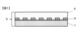
- FIG. 1 is a schematic view schematically showing an example of the wiring board 5 of the present invention.
- the wiring board 5 has a transparent substrate 1, an opaque wiring electrode 2 patterned on at least one surface of the transparent substrate 1, a transparent substrate 1, and a transparent protective layer 4 formed on the opaque wiring electrode 2. Each will be described below.
- the transparent substrate is transparent in the visible light region.
- transparent means that the transmittance at a wavelength of 550 nm is 80% or more.
- the transmittance at a wavelength of 550 nm can be measured using an ultraviolet-visible spectrophotometer (manufactured by Hitachi High-Technologies Corporation, U-3310).
- the transparent substrate examples include a transparent substrate having no flexibility and a transparent substrate having flexibility.
- the transparent substrate having no flexibility examples include quartz glass, soda glass, chemically strengthened glass, "Pyrex (registered trademark)" glass, synthetic quartz plate, epoxy resin substrate, polyetherimide resin substrate, and polyetherketone resin. Examples thereof include a substrate and a polysulfone-based resin substrate.
- the flexible transparent substrate include a transparent film made of a resin such as a polyethylene terephthalate film (hereinafter, “PET film”), a cycloolefin polymer film, a polyimide film, a polyester film, and an aramid film, and an optical resin plate. Can be mentioned. A plurality of these may be stacked and used, and for example, a plurality of transparent substrates may be used by adhering them together with an adhesive layer.
- PET film polyethylene terephthalate film
- an inorganic film having a thickness of 5 to 50 nm on the surface of the transparent substrate It is preferable to have an inorganic film having a thickness of 5 to 50 nm on the surface of the transparent substrate.
- the inorganic film examples include silicon dioxide and niobium pentoxide.
- the adhesion between the transparent substrate and the transparent protective layer can be improved.
- the thickness of the inorganic film is more preferably 30 nm or less.
- the thickness of the inorganic film is preferably 5 nm or more from the viewpoint of adhesion.
- the thickness of the transparent substrate is appropriately selected according to the material within the range of being able to stably support the opaque wiring electrode and having the above-mentioned transparency.
- 300 ⁇ m or more is preferable in the case of a transparent substrate having no flexibility such as glass, and 25 ⁇ m in the case of a transparent substrate having flexibility such as PET film. The above is preferable.
- 1500 ⁇ m or less is preferable for a transparent substrate having no flexibility such as glass, and 300 ⁇ m or less is preferable for a transparent substrate having flexibility such as PET film. preferable.
- ⁇ Opaque wiring electrode> The opaque wiring electrodes are patterned on at least one side of the transparent substrate.
- “opaque” means that the transmittance at a wavelength of 550 nm is 25% or less.
- the material constituting the opaque wiring electrode examples include metals such as silver, gold, copper, platinum, lead, tin, nickel, aluminum, tungsten, molybdenum, chromium, titanium and indium, and alloys thereof. Among these, silver, copper and gold are preferable from the viewpoint of conductivity. Further, the opaque wiring electrode may be a cured conductive composition containing conductive particles. In this case, the shape of the conductive particles is preferably spherical, and the above-mentioned metal or alloy can be used as the material.
- the average particle size of the conductive particles is preferably 0.01 ⁇ m or more, more preferably 0.03 ⁇ m or more, 0.05 ⁇ m or more, and 0.10 ⁇ m or more from the viewpoint of improving the dispersibility of the conductive particles.
- 1.5 ⁇ m or less is preferable, and 1.0 ⁇ m or less is more preferable.
- the average particle size of the conductive particles was 100 randomly selected by magnifying the conductive particles at a magnification of 15,000 times using a scanning electron microscope (SEM) or a transmission electron microscope (TEM). It can be obtained by measuring the major axis length of each of the conductive particles and calculating the number average value thereof.
- the conductive composition preferably contains an alkali-soluble resin.
- an alkali-soluble resin By containing the alkali-soluble resin, fine opaque wiring electrodes can be formed by patterning by development.
- the alkali-soluble resin include resins having a hydroxy group and / or a carboxyl group.
- the resin having a hydroxy group examples include a phenol novolak resin having a phenolic hydroxy group, a novolak resin such as cresol novolak resin, a polymer of a monomer having a hydroxy group, a monomer having a hydroxy group and styrene, an acrylonitrile, an acrylic monomer and the like. And the copolymer with.
- Examples of the monomer having a hydroxy group include a monomer having a phenolic hydroxy group such as 4-hydroxystyrene and hydroxyphenyl (meth) acrylate; 2-hydroxyethyl (meth) acrylate, 2-hydroxypropyl (meth) acrylate.
- the resin having a carboxyl group examples include a carboxylic acid-modified epoxy resin, a carboxylic acid-modified phenol resin, a polyamic acid resin, a carboxylic acid-modified siloxane resin, a polymer of a monomer having a carboxyl group, a monomer having a carboxyl group and styrene, and acrylonitrile. , Polymers with acrylic monomers and the like.
- Examples of the monomer having a carboxyl group include acrylic acid, methacrylic acid, maleic acid, fumaric acid, crotonic acid, itaconic acid, citraconic acid, and cinnamon acid.
- Examples of the resin having a hydroxy group and a carboxyl group include a copolymer of a monomer having a hydroxy group and a monomer having a carboxyl group, a monomer having a hydroxy group, a monomer having a carboxyl group, and a styrene, acrylonitrile, an acrylic monomer, and the like. Examples include copolymers. Two or more of these may be contained.
- the conductive composition may contain pigments and / or dyes.
- the metallic luster of the opaque wiring electrode can be suppressed and the opaque wiring electrode can be made difficult to see without separately providing a light-shielding layer described later.
- a light-shielding layer may be provided at the same time, and the metallic luster of the opaque wiring electrode can be further suppressed.
- the content of the pigment and / or the dye is preferably 0.5 to 2.5% by mass in the conductive composition. From the viewpoint of further suppressing the metallic luster of the opaque wiring electrode, the content of the pigment and / or the dye is preferably 0.5% by mass or more. On the other hand, from the viewpoint of improving the conductivity, the content of the pigment and / or the dye is preferably 2.5% by mass or less.
- pigment examples include lactam pigment, perylene pigment, phthalocyanine pigment, isoindoline pigment, diaminoanthraquinone pigment, dioxazine pigment, indantron pigment, carbon black or inorganic pigment.
- the dye examples include ferrocene dyes, fluorenone dyes, perylene dyes, triphenylmethane dyes, coumarin dyes, diphenylamine dyes, quinacridone dyes, quinophthalone dyes, phthalocyanine dyes and xanthene dyes. ..
- the conductive composition is preferably a photosensitive conductive composition containing a photopolymerization initiator in addition to the above-mentioned conductive particles and alkali-soluble resin.
- a fine opaque wiring electrode can be formed by photolithography.
- photopolymerization initiator examples include 1,2-octanedione, 1- [4- (phenylthio) -2- (O-benzoyloxime)], 2,4,6-trimethylbenzoyl-diphenyl-phosphine oxide, and bis.
- the conductive composition further comprises a dispersant, a monomer having an unsaturated double bond, a photoacid generator, a thermoacid generator, a sensitizer, an adhesion improver, a surfactant, a thermosetting agent, and the like. It may contain a polymerization inhibitor or the like.
- Examples of the monomer having an unsaturated double bond include methyl acrylate, ethyl acrylate (hereinafter, “EA”), acrylic acid (hereinafter, “AA”), 2-ethylhexyl acrylate, n-butyl acrylate, and i-butyl.
- Examples of the pattern shape of the opaque wiring electrode include a mesh shape and a stripe shape. Above all, a mesh shape is preferable from the viewpoint of making the conductivity of the pattern uniform.
- the opaque wiring electrode is more preferably a metal mesh composed of the above-mentioned metal and having a mesh-like pattern.
- Examples of the mesh shape include a grid-like shape in which the unit shape is a triangle, a quadrangle, a polygon, a circle, or a combination of these unit shapes.
- the area of the portion where the opaque wiring electrode is formed is preferably 20% or less, more preferably 15% or less with respect to the transparent substrate.
- Two or more opaque wiring electrodes can be formed via the transparent protective layer. By using two layers of opaque electrodes, it is possible to reduce the area of the portion where the opaque wiring electrodes are formed.
- the thickness of the opaque wiring electrode is preferably 0.01 ⁇ m or more, more preferably 0.05 ⁇ m or more, still more preferably 0.1 ⁇ m or more.
- the thickness of the opaque wiring electrode is preferably 10 ⁇ m or less, more preferably 5 ⁇ m or less, still more preferably 3 ⁇ m or less, from the viewpoint of forming fine wiring.
- the line width of the opaque wiring electrode is preferably 1 to 10 ⁇ m. When the line width of the opaque wiring electrode is 1 ⁇ m or more, the conductivity can be improved.
- the line width of the opaque wiring electrode is more preferably 1.5 ⁇ m or more, further preferably 2 ⁇ m or more. On the other hand, when the line width of the opaque wiring electrode is 10 ⁇ m or less, the opaque wiring electrode can be made less visible.
- the line width of the opaque wiring electrode is more preferably 7 ⁇ m or less, further preferably 6 ⁇ m or less.
- the line width of the opaque wiring electrode can be measured using an optical microscope (VHX-6000 manufactured by KEYENCE CORPORATION).
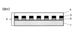
- the light-shielding layer 3 As shown in FIG. 2, it is preferable to have the light-shielding layer 3 on the upper part of the opaque wiring electrode 2.
- the light-shielding layer include a black sputtering film of an alloy such as nickel, titanium, and copper, plating, and a cured film of a resin composition containing a black pigment.
- a cured film of a resin composition containing a black pigment is preferable from the viewpoint of suppressing reflection in the opaque wiring electrode forming region.
- the light-shielding layer may have conductivity, and the light-shielding layer having conductivity can improve the conductivity of the opaque wiring electrode.
- Plating can be formed on the surface of the opaque wiring electrode, for example, by contacting the opaque wiring electrode with an aqueous hydrochloric acid solution containing palladium, tellurium and / or a compound thereof.
- Aqueous hydrochloric acid containing palladium, tellurium and / or a compound thereof has a pH of 3 or less from the viewpoint of effectively producing plating by a redox reaction between palladium and / or tellurium and a metal in an opaque wiring electrode. It is preferably present, and the pH is more preferably 2 or less.
- the resin composition includes an alkali-soluble resin, a dispersant, a monomer having an unsaturated double bond, a photopolymerization initiator, and a photoacid generator.
- a thermoacid generator, a sensitizer, an adhesion improver, a surfactant, a thermosetting agent, a polymerization inhibitor, a leveling agent and the like may be contained.
- those exemplified in the description of the opaque wiring electrode can be used.
- the resin composition containing the black pigment is preferably a positive photosensitive resin composition containing an alkali-soluble resin and a photoacid generator.
- positive photosensitive refers to the property that the chemical structure is changed by irradiation with active light and becomes soluble in an alkaline developer. Since the resin composition containing the black pigment is a positive photosensitive resin composition, a light-shielding layer having the same pattern can be easily formed on the opaque wiring electrode by the method described later.
- photoacid generator examples include diazonium salt, diazoquinone sulfonic acid amide, diazoquinone sulfonic acid ester, diazoquinone sulfonate, nitrobenzyl ester, onium salt, halide, halide, isocyanate halide, triazine halide, and bisarylsulfonyldiazomethane. , Disulfone and the like.
- black pigment examples include organic pigments and inorganic pigments, and two or more of these pigments may be contained.
- organic pigment examples include soluble azo pigment, insoluble azo pigment, metal complex salt azo pigment, phthalocyanine pigment, condensed polycyclic pigment and the like.
- the inorganic pigment examples include carbon black, graphite, pine smoke, iron oxide such as iron black, hematite, Gesite, and magnetite, titanium, chromium, lead, and a metal composite system thereof.
- carbon black is preferable because it has a high light-shielding property.
- the content of the black pigment is preferably 5 to 30% by mass in the solid content of the resin composition.
- the content of the black pigment is 5% by mass or more, the light-shielding property can be further improved.
- the content of the black pigment is 30% by mass or less, the sensitivity to exposure is improved and the solubility is improved.
- the content of the black pigment is more preferably 15% by mass or less.
- “solubility” is the ease of dissolving the exposed portion in the developing solution, and the better the solubility, the faster the exposed portion dissolves in the developing solution.
- the light-shielding layer may be formed directly on the opaque wiring electrode, or may be formed on the opaque wiring electrode via a transparent protective layer.
- the transparent protective layer is transparent in the visible light region.
- the definition of transparency is as described above. If it is difficult to measure with only the transparent protective layer due to the thin film, a transparent protective layer is formed on the non-alkali glass "AN Wizus (registered trademark)" (manufactured by AGC Inc.), and the obtained sample is prepared. It can be obtained by measuring the transmittance.
- the transparent protective layer may have ion migration resistance and adhesiveness, and may be a multilayer including the same layer or two or more different layers. Above all, an insulating layer having ion migration resistance is preferable from the viewpoint of suppressing the occurrence of a short circuit due to ion migration between adjacent opaque wiring electrodes. Ion migration resistance here refers to the short circuit caused by ion migration between electrodes that occurs when positive and negative electrical terminals are connected to two electrodes that are not electrically connected and a voltage is applied. Refers to resistance.
- the transparent protective layer is an adhesive layer having adhesiveness, it can be bonded to a cover material such as a cover glass or a cover plastic.
- the transparent protective layer is only an insulating layer, it cannot be bonded to the cover material, and if it is only an adhesive layer, a short circuit due to ion migration is likely to occur, but the insulating layer and adhesive are on the transparent substrate. By stacking the layers in this order, it is possible to achieve both ion migration resistance and adhesiveness.
- the insulating layers are laminated in the same number as the number of layers of the opaque wiring electrodes from the viewpoint of ion migration resistance, and the opaque wiring electrodes are transparent.
- the insulating layer, the insulating layer, and the adhesive layer are laminated in this order on the transparent substrate.
- two or more transparent protective layers are laminated, at least one of the transparent protective layers is an insulating layer having ion migration resistance, and at least one layer is an adhesive layer having adhesiveness, and the transparent layer is said to be transparent. It is preferable that the substrate, the insulating layer, and the adhesive layer are laminated in this order, and the refractive index n2a of the insulating layer and the refractive index n2b of the adhesive layer satisfy the following formula (2). 0.97 ⁇ n2a / n2b ⁇ 1.03 (2).
- an insulating resin material such as a polyimide resin, an acrylic resin, a cardo resin, an epoxy resin, a melamine resin, a urethane resin, a silicone resin, a fluororesin, an inorganic material such as glass, etc. Is preferably used. Two or more of these may be used. Above all, an insulating resin material is preferable from the viewpoint of strength against bending and bending of the transparent substrate.
- acrylic resin silicone resin, urethane resin, polyamide resin, polyvinyl ether fat, vinyl acetate / vinyl chloride copolymer, modified polyolefin resin, fluororesin, natural rubber, synthetic rubber and the like are suitable. Used for. Two or more of these may be used.
- the transparent protective layer may be formed on the transparent substrate and the opaque wiring electrode by the method for forming the transparent protective layer described later using the transparent resin composition.
- the transparent resin composition includes an alkali-soluble resin, a dispersant, a monomer having an unsaturated double bond, a photopolymerization initiator, a photoacid generator, a thermoacid generator, a sensitizer, an adhesion improver, a surfactant, and the like. It may contain a thermosetting agent, a polymerization inhibitor, a leveling agent and the like. Above all, it is preferable to exhibit photosensitivity by containing an alkali-soluble resin and a photopolymerization initiator. For each component, those exemplified in the description of the opaque wiring electrode can be used.
- the internal reflectance R1 in the opaque wiring electrode forming portion measured from the transparent protective layer side is 0.1% or less, preferably 0.01% or more and 0.1% or less.
- the internal reflectance R1 can be calculated as follows. First, as shown in FIG. 3, an antireflection film 6 is attached to the surface of the transparent protective layer 4 of the wiring substrate 5, and a black film 7 is attached to the surface of the transparent substrate 1, the transparent protective layer 4 and the air interface, and the transparent substrate 1 are attached. Prepare a first reflectance evaluation substrate with reduced reflection at the air interface. Next, the reflectance R3 is measured from the transparent protective layer 4 side of the opaque wiring electrode forming region of the first reflectance evaluation substrate 8. Then, as shown in FIG. 4, the reflectance R4 is measured in the same manner for the opaque wiring electrode non-formed region of the first reflectance evaluation substrate 8.
- R3-R4 is obtained, and this value is used as the internal reflectance R1.
- the rate R1 can be calculated.
- Each reflectance can be measured using a spectrocolorimeter.
- the transparent substrate has an opaque wiring electrode and a transparent protective layer on both sides, and the opaque wiring electrode forming portion measured from each transparent protective layer side.
- the antireflection film 6 is attached to the surface of the transparent protective layer 4 on the side having the lower reflectance R3, and the black film 7 is attached to the surface of the other transparent protective layer 4, so that the first reflection is performed.
- the internal reflectance R1 can be obtained.
- Examples of the method of reducing the internal reflectance R1 to 0.1% or less include a method of containing a pigment and / or a dye in the opaque wiring electrode, a method of providing a light-shielding layer on the opaque wiring electrode, and the like.
- the refractive index n1 of the transparent substrate and the refractive index n2 of the transparent protective layer satisfy the following formula (1).
- the refractive index n1 and the refractive index n2 satisfy the following formula (1), the reflection at the interface between the transparent protective layer and the transparent substrate is suppressed, and the difference between the reflection and the reflection at the opaque wiring electrode forming portion is reduced. This makes it difficult for the opaque wiring electrode to be visually recognized. 0.97 ⁇ n2 / n1 ⁇ 1.03 (1).
- the refractive index n1 of the transparent substrate and the refractive index n2 of the transparent protective layer can be obtained by measuring the refractive index at a wavelength of 550 nm using a prism coupler (manufactured by Metricon, PC-2000). If it is difficult to measure with only the transparent protective layer due to the thin film, it can be obtained by forming the transparent protective layer on the silicon wafer and then measuring the refractive index of the transparent protective layer on the silicon wafer. .. When two or more transparent protective layers are laminated, the refractive index of the transparent protective layer in contact with the transparent substrate is set to n2.
- R1: R2 1: 3 to 3: 1.
- the reflectance R2 can be calculated as follows. First, as shown in FIG. 5, an antireflection film 6 is attached to one surface of the transparent substrate 1 and a black film 7 is attached to the other surface of the transparent substrate 1 to reduce reflection between both sides of the transparent substrate 1 and the air interface.
- the second reflectance evaluation substrate 9 is prepared. With respect to the obtained second reflectance evaluation substrate 9, the reflectance R5 is measured from the antireflection film 6 side. R4-R5 is obtained from the obtained reflectance R5 and the above-mentioned reflectance R4, and this value is taken as the reflectance R2 at the interface between the transparent protective layer and the transparent substrate.
- a method for evaluating the ion migration resistance of the wiring board for example, it can be evaluated by the following method. First, an opaque wiring electrode pattern having a line line width of 10 ⁇ m and a line space of 10 ⁇ m as shown in FIG. 13 is formed, a transparent protective layer is formed on the wiring portion of the opaque wiring electrode, and a substrate for ion migration resistance evaluation is prepared. Connect positive and negative electric terminals to the terminals of the obtained ion migration resistance evaluation board, put them in a constant temperature and humidity chamber at 85 ° C and 85 RH% while passing a direct current at 5 V, and evaluate the transition of electric resistance.
- the time when the electrical resistance becomes 15630 ⁇ or less is defined as the short-circuit time, and it can be evaluated that the shorter the short-circuit time, the lower the ion migration resistance, and the longer the short-circuit time, the higher the ion migration resistance.
- 6 to 9 and 12 show schematic views of another example of the configuration of the wiring board of the present invention.
- FIG. 6 has a first opaque wiring electrode 2 on the transparent substrate 1, a first transparent protective layer 4 on the first opaque wiring electrode 2, and a first transparent protective layer 4 on the first transparent protective layer 4. It is a schematic diagram of the wiring board which has the second opaque wiring electrode 2 and the second transparent protective layer 4.
- FIG. 7 has a first opaque wiring electrode 2 on the transparent substrate 1, a first transparent protective layer 4 on the first opaque wiring electrode 2, and a first transparent protective layer 4 on the first transparent protective layer 4.
- FIG. 8 is a schematic diagram of a wiring board having opaque wiring electrodes 2 on both sides of the transparent substrate 1 and a transparent protective layer 4 on the opaque wiring electrodes 2 on both sides of the transparent substrate 1.
- FIG. 9 has opaque wiring electrodes 2 on both sides of the transparent substrate 1, a light-shielding layer 3 on the opaque wiring electrodes 2 on one side, and on the opaque wiring electrodes 2 and the light-shielding layer 3 on both sides of the transparent substrate 1.
- FIG. 12 has an opaque wiring electrode 2 on one side of the transparent substrate 1, a first transparent protective layer 4 on the opaque wiring electrode 2, and a second transparent protective layer on the first transparent protective layer 4. It is a schematic diagram of the wiring board having 4.
- an opaque wiring electrode is formed on at least one side of the transparent substrate.
- the opaque wiring electrodes may be formed on both sides of the transparent substrate.
- the step of forming the opaque wiring electrode on at least one side of the transparent substrate is the step of forming the first opaque wiring electrode on one side of the transparent substrate, and the step of forming the transparent protective layer on the first opaque wiring electrode. Further, it may have a step of forming a second opaque wiring electrode on the transparent protective layer.
- Examples of the method for forming the opaque wiring electrode include a method of forming a pattern by a photolithography method using the above-mentioned photosensitive conductive composition, screen printing, gravure printing, inkjet printing using the conductive composition (conductive paste), and the like. Examples thereof include a method of forming a pattern using a metal, a metal composite, a composite of a metal and a metal compound, a method of forming a film of a metal alloy, and the like, and forming the film by a photolithography method using a resist. Among these, since fine wiring can be formed, a method of forming by a photolithography method using a photosensitive conductive composition is preferable. When the opaque wiring electrodes are formed on both sides of the transparent substrate, or when two or more opaque wiring electrodes are formed via the transparent protective layer, each opaque wiring electrode may be formed by the same method or different. The methods may be combined.
- the method of forming a pattern by a photolithography method using a photosensitive conductive composition includes a coating step of applying the photosensitive conductive composition on a transparent substrate to obtain a coating film, and an exposure and development of the coating film. It is manufactured by a photolithography step of obtaining a pattern and a curing step of heating the pattern at 100 to 300 ° C. to obtain a conductive pattern.
- the coating step is a step of coating the above-mentioned photosensitive conductive composition on a transparent substrate to obtain a coating film.
- a method of applying the photosensitive conductive composition to a transparent substrate for example, rotary coating using a spinner, spray coating, roll coating, screen printing, or slit coater, blade coater, die coater, calendar coater, meniscus coater Alternatively, application using a bar coater can be mentioned.
- the obtained coating film may be dried to remove the solvent.
- the method for drying the coating film include heat drying by oven, hot plate or infrared irradiation, or vacuum drying. Generally, the heating and drying temperature is 50 to 120 ° C., and the heating and drying time is 1 minute to several hours.
- the photolithography process is a process of exposing and developing the coating film obtained in the coating process to obtain a pattern.
- the light source used for the exposure of the coating film i-line (365 nm), h-line (405 nm) or g-line (436 nm) of a mercury lamp or an LED lamp is preferable.
- a conductive pattern can be obtained by exposing the surface coated with the photosensitive conductive composition on the transparent substrate through an exposure mask and removing the unexposed portion with a developing solution.
- Examples of the developing solution for alkaline development include tetramethylammonium hydroxide, diethanolamine, diethylaminoethanol, sodium hydroxide, potassium hydroxide, sodium carbonate, potassium carbonate, triethylamine, diethylamine, methylamine, dimethylamine, and dimethyl acetate.
- Examples thereof include aqueous solutions of aminoethyl, dimethylaminoethanol, dimethylaminoethylmethacrylate, cyclohexylamine, ethylenediamine or hexamethylenediamine, and these aqueous solutions include N-methyl-2-pyrrolidone, N, N-dimethylformamide, N, N.
- -Polar solvents such as dimethylacetamide, dimethylsulfoxide or ⁇ -butyrolactone, alcohols such as methanol, ethanol or isopropanol, esters such as ethyl lactate or propylene glycol monomethyl ether acetate, cyclopentanone, cyclohexanone, isobutylketone or methylisobutylketone.
- ketones or surfactants may be added.
- Examples of the developing solution for organic development include N-methyl-2-pyrrolidone, N-acetyl-2-pyrrolidone, N, N-dimethylacetamide, N, N-dimethylformamide, dimethyl sulfoxide or hexamethylphosphortri.
- Examples thereof include a polar solvent such as amide, or a mixed solution of these polar solvents with methanol, ethanol, isopropyl alcohol, xylene, water, methylcarbitol or ethylcarbitol.
- a developing method for example, a method of spraying the developer on the surface of the coating film while the substrate is allowed to stand or rotate, a method of immersing the substrate in the developer, or a method of immersing the substrate in the developer.
- a method of applying an ultrasonic wave can be mentioned.
- the pattern obtained in the developing step may be rinsed with a rinsing solution.
- a rinsing solution examples include water or an aqueous solution in which alcohols such as ethanol or isopropyl alcohol, esters such as ethyl lactate or propylene glycol monomethyl ether acetate, or a surfactant are added to water or water.
- the positive photosensitive resin composition containing a black pigment is applied onto the opaque wiring electrode formed on the transparent substrate, and then the black color is used as a mask.
- a light-shielding layer having the same pattern as the opaque wiring electrode can be formed. If necessary, it is necessary to secure continuity with an external element such as a terminal portion, and when removing the light-shielding layer in the portion where the opaque wiring electrode is to be exposed, the positive photosensitive resin composition is formed by using an exposure mask. It may have a step of exposing from the coated surface side of the object.
- a curing process may be included in the manufacturing process of the light-shielding layer.
- the cure temperature is preferably 100 to 300 ° C.
- Examples of the curing method include heating and drying with an oven, an inert oven or a hot plate, heating and drying with an electromagnetic wave such as an infrared heater, and vacuum drying.
- a transparent protective layer is formed on the transparent substrate and the opaque wiring electrode.
- Examples of the method for forming the transparent protective layer include a method of applying a transparent resin composition and drying it, and a method of attaching a transparent adhesive film to the opaque wiring electrode forming surface side.
- Examples of the method for applying the transparent resin composition include rotary coating using a spinner, spray coating, roll coating, screen printing, offset printing, gravure printing, letterpress printing, flexographic printing, blade coater, die coater, calendar coater, and Menis Casco.
- rotary coating using a spinner spray coating, roll coating, screen printing, offset printing, gravure printing, letterpress printing, flexographic printing, blade coater, die coater, calendar coater, and Menis Casco.
- -A method using a ter or bar coater can be mentioned.
- the dried film can be cured by ultraviolet treatment and / or heat treatment.
- the transparent resin composition may have photosensitivity. For example, when it is necessary to secure continuity with an external element such as a terminal portion and the transparent protective layer of the portion where the opaque wiring electrode is to be exposed is removed, it is removed by a photolithography step as in the case of the photosensitive conductive composition. be able to.
- the materials used in each example and comparative example are as follows.
- the transmittance of the transparent substrate at a wavelength of 550 nm was measured using an ultraviolet-visible spectrophotometer (U-3310, manufactured by Hitachi High-Technologies Corporation).
- the refractive index at a wavelength of 550 nm was measured at room temperature of 23 ° C. using a prism coupler (manufactured by Metricon, PC-2000).
- Zirconia dispersion "Zircoster (registered trademark)” ZP-153 (manufactured by Nippon Shokubai Co., Ltd.).
- PET film "Lumirror (registered trademark)” T60 (manufactured by Toray Industries, Inc.).
- Silver fine particles with a particle size of 40 nm are added and mixed with a rotating-revolving vacuum mixer "Awatori Rentaro ARE-310" (manufactured by Shinky Co., Ltd.) to obtain 100.0 g of photosensitive material.
- a reactive conductive paste (D-1) was obtained.
- the obtained photosensitive insulating paste (E-6) was applied onto a 4-inch silicone wafer, and the refractive index was measured at a room temperature of 23 ° C. at a wavelength of 550 nm using a prism coupler (manufactured by Metricon, PC-2000). It was 1.66.
- ⁇ Reflectance R1 measurement> For the first wiring substrate obtained in each Example and Comparative Example, an antireflection film was attached to the surface of the transparent protective layer by a rubber roller in order to suppress reflection at the interface between the transparent protective layer and the air. Further, in order to suppress reflection at the interface between the transparent substrate and the air, a black film was attached to the surface of the transparent substrate with a rubber roller to prepare a first reflectance evaluation substrate as shown in FIG. The reflectance R3 was measured from the transparent protective layer side in the opaque wiring electrode forming region of the obtained first reflectance evaluation substrate. Further, as shown in FIG. 4, the reflectance R4 was similarly measured for the opaque wiring electrode non-forming portion region of the first reflectance evaluation substrate.
- R3-R4 was calculated and used as the reflectance R1.
- the reflectances R3 and R4 were determined by measuring the visual reflectance (Y value) of a D65 light source and a 10 ° field using a spectrocolorimeter (CM-2500d) manufactured by Konica Minolta Sensing Co., Ltd.
- ⁇ Reflectance R2 measurement> For the transparent substrate used in each Example and Comparative Example, an antireflection film was attached to one surface of the transparent substrate by a rubber roller. Further, a black film was attached to the other surface of the transparent substrate by a rubber roller to prepare a second reflectance evaluation substrate as shown in FIG. With respect to the obtained second reflectance evaluation substrate, the reflectance R5 was measured from the antireflection film side. R4-R5 was calculated from the obtained reflectance R5 and the reflectance R4, and this was used as the reflectance R2.
- the reflectance R5 was determined by measuring the visual reflectance (Y value) of a D65 light source and a 10 ° field using a spectrocolorimeter (CM-2500d) manufactured by Konica Minolta Sensing Co., Ltd.
- R3-R5 was calculated from the obtained reflectance R5 and the reflectance R3, and this was used as the reflectance R in the opaque wiring electrode forming region.
- the reflectance R is less than 0.12%, it is “A”, when it is 0.12% or more and less than 0.16%, it is “B”, and when it is 0.16% or more and less than 0.26%, it is “A”.
- ⁇ Adhesive evaluation> For the first wiring substrate obtained in each Example and Comparative Example, a PET film was attached to the surface of one of the transparent protective layers with a rubber roller, and the adhesive / film peeling analyzer VPA (manufactured by Kyowa Interface Science Co., Ltd.) was peeled off. The adhesive strength was measured under the conditions of a speed of 300 mm / min and a peeling angle of 180 °. When the adhesive strength was 3.0 N / 25 mm or more, it was evaluated as "A”, and when it was less than 3.0 N / 25 mm, it was evaluated as "B".
- Example 1 [Manufacturing the first wiring board] ⁇ Formation of opaque wiring electrode>
- the photosensitive conductive paste (D-1) obtained in Production Example 3 is applied to one side of the transparent substrate (a-1) by spin coating so that the film thickness becomes 1 ⁇ m after drying, and the temperature is 90 ° C. 8 Allowed to dry for minutes.
- an exposure apparatus PEM-6M; Union Optical Co., Ltd.
- PEM-6M Union Optical Co., Ltd.
- an exposure mask having a mesh-shaped mask mesh portion having a mesh pitch of 150 ⁇ m and a mesh angle of 90 degrees and a mask shading portion.
- the mask opening width was 4 ⁇ m. Then, using a 0.1% tetramethylammonium hydroxide aqueous solution as a developing solution, development is carried out for twice the time for which the exposed part is dissolved, further rinsed with ultrapure water for 30 seconds, and then a box oven at 240 ° C. Was heated for 60 minutes to obtain a substrate with an opaque wiring electrode. As a result of measuring the obtained opaque wiring electrode line width with an optical microscope, it was 4 ⁇ m.
- the light-shielding paste obtained from Production Example 6 was applied to the opaque wiring electrode-forming surface of the obtained substrate with the opaque wiring electrode by spin coating so that the thickness of the light-shielding layer after drying was 0.5 ⁇ m.
- the mixture was dried at ° C. for 5 minutes and exposed to an exposure amount of 500 mJ / cm 2 (wavelength 365 nm conversion) from the opposite side of the opaque wiring electrode forming surface using the opaque wiring electrode as a mask.
- a 2.38% tetramethylammonium hydroxide aqueous solution was immersed in a developing solution for 50 seconds to develop, and a light-shielding layer was formed on the upper part of the opaque wiring electrode. Further, it was heated in a box oven at 240 ° C. for 60 minutes to obtain a substrate with a light-shielding layer.
- the photosensitive insulating paste (E-1) obtained in Production Example 8 is spin-coated on the opaque wiring electrode and the light-shielding layer forming surface of the obtained substrate with a light-shielding layer so that the film thickness becomes 1.5 ⁇ m after drying. And dried at 80 ° C. for 5 minutes. An exposure was made through an exposure mask using an exposure apparatus (PEM-6M; manufactured by Union Optical Co., Ltd.) at an exposure amount of 100 mJ / cm 2 (wavelength 365 nm conversion).
- PEM-6M manufactured by Union Optical Co., Ltd.
- FIG. 1 The first wiring board as shown in is obtained. Using the obtained first wiring substrate, visibility evaluation, reflectance R1 measurement, reflectance R evaluation in the opaque wiring electrode forming region, adhesiveness evaluation, and adhesion evaluation were performed.
- FIG. 2 shows the same as in Example 1 except that the patterns of the transparent substrate, the photosensitive insulating paste used for forming the transparent protective layer, and the exposure mask used for forming the opaque wiring electrode were changed as shown in Table 1.
- the first wiring board and the second wiring board as described above were manufactured.
- Example 8 [Manufacturing the first wiring board] ⁇ Formation of opaque wiring electrode>
- Example 1 except that the photosensitive conductive paste (D-1) was changed to the photosensitive conductive paste (D-2), a pattern having a mesh shape of 450 ⁇ m and an angle of 90 degrees was used, and the mask opening width was 12 ⁇ m.
- a substrate with an opaque wiring electrode was obtained in the same manner as in ⁇ Formation of opaque wiring electrode>. As a result of measuring the obtained opaque wiring electrode line width with an optical microscope, it was 12 ⁇ m.
- a transparent protective layer is formed on the opaque wiring electrode forming surface of the obtained substrate with opaque wiring electrodes in the same manner as in ⁇ Formation of transparent protective layer> of Example 1, and a first wiring board as shown in FIG. 1 is formed. Obtained.
- Example 9 The first wiring board and the second wiring board as shown in FIG. 1 were produced in the same manner as in Example 8 except that the photosensitive insulating paste used for forming the transparent protective layer was changed as shown in Table 1. did.
- Example 10 [Manufacturing the first wiring board] ⁇ Formation of opaque wiring electrode> A substrate with an opaque wiring electrode was obtained in the same manner as in Example 1 except that a pattern having a mesh shape with a pitch of 450 ⁇ m and an angle of 90 degrees was used and the mask opening width was 12 ⁇ m. As a result of measuring the opaque wiring electrode line width with an optical microscope, it was 12 ⁇ m.
- Example 11 [Manufacturing the first wiring board] ⁇ Formation of first opaque wiring electrode> A substrate with an opaque wiring electrode (hereinafter referred to as the first opaque wiring electrode in this embodiment) was obtained in the same manner as in Example 1 except that a pattern having a mesh shape of 300 ⁇ m and an angle of 90 degrees was used. As a result of measuring the first opaque wiring electrode line width with an optical microscope, it was 4 ⁇ m.
- a second opaque wiring electrode is formed on the first transparent protective layer forming surface of the obtained substrate with the transparent protective layer in the same manner as the formation of the first opaque wiring electrode, and the second opaque wiring electrode is formed. Obtained a substrate with. As a result of measuring the second opaque wiring electrode line width with an optical microscope, it was 4 ⁇ m.
- a light-shielding layer was formed at a portion corresponding to the opaque wiring electrode on the second opaque wiring electrode forming surface of the obtained substrate with the opaque wiring electrode in the same manner as in ⁇ Formation of light-shielding layer> of Example 1. .. Further, it was heated in a box oven at 240 ° C. for 60 minutes to obtain a substrate with a light-shielding layer.
- a second transparent protective layer is formed on the opaque wiring electrode and the light-shielding layer forming surface of the obtained substrate with a light-shielding layer in the same manner as in ⁇ Formation of the first transparent protective layer>, and the wiring board as shown in FIG. Got
- the exposure mask used in ⁇ formation of the first opaque wiring electrode> was changed to one having a line line width of 10 ⁇ m and a line space of 10 ⁇ m as shown in FIG. 13, and during exposure in ⁇ formation of the first transparent protective layer>.
- the point that the terminal part was shielded from light the point that the exposure mask used in ⁇ formation of the second opaque wiring electrode> was changed to the one with a line line width of 10 ⁇ m and a line space of 10 ⁇ m shown in FIG.
- a second wiring substrate was produced in the same manner as the first wiring substrate, except that the terminal portion was shielded from light during exposure at the point of re-exposure, ⁇ formation of the second transparent protective layer>.
- Example 12 Manufacturing the first wiring board] ⁇ Formation of first opaque wiring electrode> ⁇ Opaque wiring of Example 1 except that the transparent substrate (a-1) is changed to the transparent substrate (a-2), the mesh shape is a pattern with a pitch of 300 ⁇ m and an angle of 90 degrees, and the mask opening width is 4 ⁇ m. Forming the electrode>, a substrate with a first opaque wiring electrode was obtained. The obtained first opaque wiring electrode line width was measured with an optical microscope and found to be 4 ⁇ m.
- a second opaque wiring electrode is formed on the surface of the obtained substrate with the opaque wiring electrode opposite to the first opaque wiring electrode forming surface in the same manner as the formation of the first opaque wiring electrode, and the second opaque wiring electrode is formed. Obtained a substrate with. As a result of measuring the second opaque wiring electrode line width with an optical microscope, it was 4 ⁇ m.
- the opaque wiring electrode was formed on the first opaque wiring electrode forming surface of the obtained substrate with the opaque wiring electrode in the same manner as in ⁇ Formation of light-shielding layer> of Example 1 except that the exposure amount was 3000 mJ / cm 2 .
- a light-shielding layer was formed at the location corresponding to. Further, it was heated in a box oven at 240 ° C. for 60 minutes to obtain a substrate with a light-shielding layer.
- a second transparent protective layer is formed on the second opaque wiring electrode forming surface of the obtained substrate with the transparent protective layer in the same manner as in ⁇ Formation of the first transparent protective layer>, and is shown in FIG. I got a wiring board like this.
- Example 13 The first wiring board as shown in FIG. 2 and the same as in Example 1 except that silicon dioxide was sputtered on one side of the transparent substrate (a-1) using a sputtering device so as to have a thickness of 1 nm. A second wiring board was manufactured.
- Example 14 A first wiring board and a second wiring board as shown in FIG. 2 were produced in the same manner as in Example 13 except that the thickness of silicon dioxide was changed as shown in Table 2.
- Example 18 [Manufacturing the first wiring board] ⁇ Formation of opaque wiring electrode> A substrate with an opaque wiring electrode was obtained in the same manner as in Example 14. The obtained first opaque wiring electrode line width was measured with an optical microscope and found to be 4 ⁇ m.
- a substrate with a light-shielding layer was obtained on the opaque wiring electrode forming surface of the obtained substrate with opaque wiring electrodes in the same manner as in Example 1.
- the first transparent protective layer was formed in the same manner as in ⁇ Formation of transparent protective layer> of Example 1 except that the photosensitive insulating paste (E-1) was changed to the photosensitive insulating paste (E-3). A substrate with a first transparent protective layer was obtained.
- a transparent adhesive film (b-1) was attached to the first transparent protective layer forming surface of the obtained substrate with the transparent protective layer by a rubber roller to form a second transparent protective layer, which is shown in FIG.
- a first wiring board as shown was produced.
- the exposure mask used in ⁇ Formation of opaque wiring electrode> was changed to the one shown in FIG. 13 having a line line width of 10 ⁇ m and a line space of 10 ⁇ m.
- a substrate was prepared.
- Example 19 A first wiring board and a second wiring board as shown in FIG. 12 were produced in the same manner as in Example 18 except that the second transparent protective layer (b-1) was changed to (b-2).
- Example 20 [Manufacturing the first wiring board] ⁇ Formation of opaque wiring electrode> A substrate with an opaque wiring electrode was obtained in the same manner as in ⁇ Formation of an opaque wiring electrode> in [Preparation of a first wiring board] in Example 14. The obtained first opaque wiring electrode line width was measured with an optical microscope and found to be 4 ⁇ m.
- a substrate with a light-shielding layer was obtained on the opaque wiring electrode-forming surface of the obtained substrate with an opaque wiring electrode in the same manner as in ⁇ Formation of a light-shielding layer> in Example 14.
- a transparent adhesive film (b-2) was attached to the light-shielding layer-forming surface of the obtained light-shielding layered substrate with a rubber roller to form a transparent protective layer, and a first wiring board as shown in FIG. 2 was produced. ..
- Example 1 The first wiring board and the second wiring board as shown in FIG. 1 were formed in the same manner as in Example 8 except that the photosensitive conductive paste used for forming the opaque wiring electrode was changed as shown in Table 3. Made.
- Example 2 The first wiring board and the second wiring board as shown in FIG. 2 are the same as in Example 1 except that the photosensitive insulating paste used for forming the transparent substrate and the transparent protective layer is changed as shown in Table 3. A wiring board was manufactured.
- Transparent substrate 2 Opaque wiring electrode 3: Light-shielding layer 4: Transparent protective layer 5: Wiring substrate 6: Antireflection film 7: Black film 8: First reflectance evaluation substrate 9: Second reflectance evaluation Substrate 10: Mask light-shielding part 11: Mask mesh part 12: Light-shielding part 13: Opening part 14: Mesh pitch 15: Mesh angle 16: Terminal part 17: Wiring part
Landscapes
- Engineering & Computer Science (AREA)
- Microelectronics & Electronic Packaging (AREA)
- General Engineering & Computer Science (AREA)
- Theoretical Computer Science (AREA)
- Manufacturing & Machinery (AREA)
- Human Computer Interaction (AREA)
- Physics & Mathematics (AREA)
- General Physics & Mathematics (AREA)
- Laminated Bodies (AREA)
Abstract
Priority Applications (4)
| Application Number | Priority Date | Filing Date | Title |
|---|---|---|---|
| CN202180084633.3A CN116602061A (zh) | 2020-12-15 | 2021-10-29 | 布线基板 |
| US18/030,828 US20230309217A1 (en) | 2020-12-15 | 2021-10-29 | Wiring board |
| EP21906167.8A EP4266840A1 (fr) | 2020-12-15 | 2021-10-29 | Carte de câblage |
| JP2021569091A JPWO2022130803A1 (fr) | 2020-12-15 | 2021-10-29 |
Applications Claiming Priority (4)
| Application Number | Priority Date | Filing Date | Title |
|---|---|---|---|
| JP2020-207270 | 2020-12-15 | ||
| JP2020207270 | 2020-12-15 | ||
| JP2021134669 | 2021-08-20 | ||
| JP2021-134669 | 2021-08-20 |
Publications (1)
| Publication Number | Publication Date |
|---|---|
| WO2022130803A1 true WO2022130803A1 (fr) | 2022-06-23 |
Family
ID=82059756
Family Applications (1)
| Application Number | Title | Priority Date | Filing Date |
|---|---|---|---|
| PCT/JP2021/040014 WO2022130803A1 (fr) | 2020-12-15 | 2021-10-29 | Carte de câblage |
Country Status (4)
| Country | Link |
|---|---|
| US (1) | US20230309217A1 (fr) |
| EP (1) | EP4266840A1 (fr) |
| JP (1) | JPWO2022130803A1 (fr) |
| WO (1) | WO2022130803A1 (fr) |
Citations (7)
| Publication number | Priority date | Publication date | Assignee | Title |
|---|---|---|---|---|
| JP2009076432A (ja) * | 2007-01-18 | 2009-04-09 | Nitto Denko Corp | 透明導電性フィルム、その製造方法及びそれを備えたタッチパネル |
| JP2010086684A (ja) * | 2008-09-30 | 2010-04-15 | Kuramoto Seisakusho Co Ltd | 透明導電配線膜付き光学薄膜 |
| JP2014021522A (ja) * | 2012-07-12 | 2014-02-03 | Dainippon Printing Co Ltd | タッチパネル基板、及び表示装置 |
| JP2015097039A (ja) * | 2013-11-15 | 2015-05-21 | 富士フイルム株式会社 | 導電性フィルム、これを備えるタッチパネル及び表示装置、並びに配線の視認性の評価方法 |
| JP2015158840A (ja) * | 2014-02-25 | 2015-09-03 | 富士フイルム株式会社 | タッチパネルおよび導電性フィルムシート |
| JP2017211826A (ja) * | 2016-05-25 | 2017-11-30 | 凸版印刷株式会社 | 配線基板、タッチパネル、カラーフィルタ基板、及び表示装置 |
| WO2018168325A1 (fr) | 2017-03-17 | 2018-09-20 | 東レ株式会社 | Procédé de fabrication d'un substrat équipé d'une électrode de câblage, et substrat équipé d'une électrode de câblage |
-
2021
- 2021-10-29 EP EP21906167.8A patent/EP4266840A1/fr active Pending
- 2021-10-29 US US18/030,828 patent/US20230309217A1/en active Pending
- 2021-10-29 JP JP2021569091A patent/JPWO2022130803A1/ja active Pending
- 2021-10-29 WO PCT/JP2021/040014 patent/WO2022130803A1/fr active Application Filing
Patent Citations (7)
| Publication number | Priority date | Publication date | Assignee | Title |
|---|---|---|---|---|
| JP2009076432A (ja) * | 2007-01-18 | 2009-04-09 | Nitto Denko Corp | 透明導電性フィルム、その製造方法及びそれを備えたタッチパネル |
| JP2010086684A (ja) * | 2008-09-30 | 2010-04-15 | Kuramoto Seisakusho Co Ltd | 透明導電配線膜付き光学薄膜 |
| JP2014021522A (ja) * | 2012-07-12 | 2014-02-03 | Dainippon Printing Co Ltd | タッチパネル基板、及び表示装置 |
| JP2015097039A (ja) * | 2013-11-15 | 2015-05-21 | 富士フイルム株式会社 | 導電性フィルム、これを備えるタッチパネル及び表示装置、並びに配線の視認性の評価方法 |
| JP2015158840A (ja) * | 2014-02-25 | 2015-09-03 | 富士フイルム株式会社 | タッチパネルおよび導電性フィルムシート |
| JP2017211826A (ja) * | 2016-05-25 | 2017-11-30 | 凸版印刷株式会社 | 配線基板、タッチパネル、カラーフィルタ基板、及び表示装置 |
| WO2018168325A1 (fr) | 2017-03-17 | 2018-09-20 | 東レ株式会社 | Procédé de fabrication d'un substrat équipé d'une électrode de câblage, et substrat équipé d'une électrode de câblage |
Also Published As
| Publication number | Publication date |
|---|---|
| US20230309217A1 (en) | 2023-09-28 |
| EP4266840A1 (fr) | 2023-10-25 |
| JPWO2022130803A1 (fr) | 2022-06-23 |
Similar Documents
| Publication | Publication Date | Title |
|---|---|---|
| KR101898955B1 (ko) | 도전 패턴 형성 부재의 제조 방법 | |
| WO2011114846A1 (fr) | Pâte conductrice photosensible et procédé de formation d'un motif conducteur | |
| KR20140115316A (ko) | 도전 페이스트 및 도전 패턴의 제조 방법 | |
| TWI733001B (zh) | 附有配線電極之基板的製造方法 | |
| WO2022130803A1 (fr) | Carte de câblage | |
| JP7035437B2 (ja) | 導電パターン付き基板の製造方法および導電パターン付き基板 | |
| JP7095803B2 (ja) | 樹脂組成物、配線基板及び導電性パターンの製造方法 | |
| JP7472601B2 (ja) | 配線電極付き基板の製造方法 | |
| KR20160062002A (ko) | 감광성 차광 페이스트 및 터치 센서용 적층 패턴의 제조 방법 | |
| CN116602061A (zh) | 布线基板 | |
| JP7322753B2 (ja) | 感光性樹脂組成物、遮光層及びタッチセンサーパネル | |
| WO2024004318A1 (fr) | Procédé de fabrication de substrat doté d'une électrode de câblage | |
| JP2011180580A (ja) | 有機−無機複合導電性パターン形成用感光性ペーストおよび有機−無機複合導電性パターンの製造方法 | |
| WO2014156677A1 (fr) | Pâte conductrice et procédé de fabrication de pâte conductrice | |
| JPWO2019065234A1 (ja) | 電極付き基板の製造方法 | |
| WO2021149410A1 (fr) | Composition de résine photosensible positive, film durci, stratifié ainsi que procédé de fabrication de celui-ci, substrat avec motif conducteur, panneau tactile, et dispositif d'affichage électroluminescent organique | |
| JP2024061122A (ja) | 配線付き基材の製造方法 | |
| JP2023123957A (ja) | 感光性樹脂組成物、配線基板および配線基板の製造方法 | |
| JP6729378B2 (ja) | 導電ペースト、タッチセンサー部材及び導電パターンの製造方法 | |
| WO2023145714A1 (fr) | Élément conducteur transparent, panneau tactile, élément d'antenne et dispositif de chauffage transparent | |
| JP2000007824A (ja) | 導電性組成物および電極形成用転写フィルム | |
| JP2019114497A (ja) | 導電ペーストおよび導電パターン形成基板の製造方法 | |
| WO2018029749A1 (fr) | Procédé de production d'un élément conducteur formant un motif |
Legal Events
| Date | Code | Title | Description |
|---|---|---|---|
| ENP | Entry into the national phase |
Ref document number: 2021569091 Country of ref document: JP Kind code of ref document: A |
|
| 121 | Ep: the epo has been informed by wipo that ep was designated in this application |
Ref document number: 21906167 Country of ref document: EP Kind code of ref document: A1 |
|
| WWE | Wipo information: entry into national phase |
Ref document number: 202180084633.3 Country of ref document: CN |
|
| NENP | Non-entry into the national phase |
Ref country code: DE |
|
| ENP | Entry into the national phase |
Ref document number: 2021906167 Country of ref document: EP Effective date: 20230717 |