WO2022102416A1 - 配線回路基板、および配線回路基板の製造方法 - Google Patents
配線回路基板、および配線回路基板の製造方法 Download PDFInfo
- Publication number
- WO2022102416A1 WO2022102416A1 PCT/JP2021/039762 JP2021039762W WO2022102416A1 WO 2022102416 A1 WO2022102416 A1 WO 2022102416A1 JP 2021039762 W JP2021039762 W JP 2021039762W WO 2022102416 A1 WO2022102416 A1 WO 2022102416A1
- Authority
- WO
- WIPO (PCT)
- Prior art keywords
- metal
- thin film
- layer
- metal thin
- metal support
- Prior art date
Links
- 238000004519 manufacturing process Methods 0.000 title claims description 24
- 229910052751 metal Inorganic materials 0.000 claims abstract description 346
- 239000002184 metal Substances 0.000 claims abstract description 346
- 239000010409 thin film Substances 0.000 claims abstract description 156
- 239000004020 conductor Substances 0.000 claims abstract description 38
- 239000000758 substrate Substances 0.000 claims description 80
- 238000000034 method Methods 0.000 claims description 53
- PXHVJJICTQNCMI-UHFFFAOYSA-N Nickel Chemical compound [Ni] PXHVJJICTQNCMI-UHFFFAOYSA-N 0.000 claims description 24
- RYGMFSIKBFXOCR-UHFFFAOYSA-N Copper Chemical compound [Cu] RYGMFSIKBFXOCR-UHFFFAOYSA-N 0.000 claims description 14
- 229910052802 copper Inorganic materials 0.000 claims description 14
- 239000010949 copper Substances 0.000 claims description 14
- 229910052759 nickel Inorganic materials 0.000 claims description 12
- RTAQQCXQSZGOHL-UHFFFAOYSA-N Titanium Chemical compound [Ti] RTAQQCXQSZGOHL-UHFFFAOYSA-N 0.000 claims description 9
- 239000010936 titanium Substances 0.000 claims description 9
- 229910052719 titanium Inorganic materials 0.000 claims description 9
- 239000010935 stainless steel Substances 0.000 claims description 8
- 229910001220 stainless steel Inorganic materials 0.000 claims description 8
- 229910000881 Cu alloy Inorganic materials 0.000 claims description 7
- PCHJSUWPFVWCPO-UHFFFAOYSA-N gold Chemical compound [Au] PCHJSUWPFVWCPO-UHFFFAOYSA-N 0.000 claims description 7
- 229910052737 gold Inorganic materials 0.000 claims description 7
- 239000010931 gold Substances 0.000 claims description 7
- 229910052782 aluminium Inorganic materials 0.000 claims description 5
- XAGFODPZIPBFFR-UHFFFAOYSA-N aluminium Chemical compound [Al] XAGFODPZIPBFFR-UHFFFAOYSA-N 0.000 claims description 5
- BQCADISMDOOEFD-UHFFFAOYSA-N Silver Chemical compound [Ag] BQCADISMDOOEFD-UHFFFAOYSA-N 0.000 claims description 4
- 229910052709 silver Inorganic materials 0.000 claims description 4
- 239000004332 silver Substances 0.000 claims description 4
- 238000009413 insulation Methods 0.000 abstract description 4
- 239000010410 layer Substances 0.000 description 209
- 239000000463 material Substances 0.000 description 28
- 239000010408 film Substances 0.000 description 26
- 238000007747 plating Methods 0.000 description 16
- 238000005530 etching Methods 0.000 description 15
- 239000000243 solution Substances 0.000 description 11
- VYZAMTAEIAYCRO-UHFFFAOYSA-N Chromium Chemical compound [Cr] VYZAMTAEIAYCRO-UHFFFAOYSA-N 0.000 description 10
- 239000011651 chromium Substances 0.000 description 10
- 229910052804 chromium Inorganic materials 0.000 description 9
- 238000004544 sputter deposition Methods 0.000 description 9
- 238000001039 wet etching Methods 0.000 description 7
- 239000011248 coating agent Substances 0.000 description 6
- 238000000576 coating method Methods 0.000 description 6
- 238000009713 electroplating Methods 0.000 description 6
- 238000007740 vapor deposition Methods 0.000 description 6
- 238000007772 electroless plating Methods 0.000 description 5
- 239000011888 foil Substances 0.000 description 5
- 229910045601 alloy Inorganic materials 0.000 description 4
- 239000000956 alloy Substances 0.000 description 4
- 230000002093 peripheral effect Effects 0.000 description 4
- 239000011347 resin Substances 0.000 description 4
- 229920005989 resin Polymers 0.000 description 4
- HEMHJVSKTPXQMS-UHFFFAOYSA-M Sodium hydroxide Chemical compound [OH-].[Na+] HEMHJVSKTPXQMS-UHFFFAOYSA-M 0.000 description 3
- 150000002739 metals Chemical class 0.000 description 3
- 238000002360 preparation method Methods 0.000 description 3
- XEEYBQQBJWHFJM-UHFFFAOYSA-N Iron Chemical compound [Fe] XEEYBQQBJWHFJM-UHFFFAOYSA-N 0.000 description 2
- -1 polyethylene terephthalate Polymers 0.000 description 2
- 238000009751 slip forming Methods 0.000 description 2
- 239000002966 varnish Substances 0.000 description 2
- 229910002651 NO3 Inorganic materials 0.000 description 1
- NHNBFGGVMKEFGY-UHFFFAOYSA-N Nitrate Chemical compound [O-][N+]([O-])=O NHNBFGGVMKEFGY-UHFFFAOYSA-N 0.000 description 1
- 239000004695 Polyether sulfone Substances 0.000 description 1
- 239000004642 Polyimide Substances 0.000 description 1
- 239000004721 Polyphenylene oxide Substances 0.000 description 1
- 239000004115 Sodium Silicate Substances 0.000 description 1
- 229910000831 Steel Inorganic materials 0.000 description 1
- 239000007864 aqueous solution Substances 0.000 description 1
- XGXDPENSUQBIDF-UHFFFAOYSA-O azanium;cerium;nitrate Chemical compound [NH4+].[Ce].[Ce].[O-][N+]([O-])=O XGXDPENSUQBIDF-UHFFFAOYSA-O 0.000 description 1
- 230000015572 biosynthetic process Effects 0.000 description 1
- 238000001312 dry etching Methods 0.000 description 1
- 238000010438 heat treatment Methods 0.000 description 1
- 238000007654 immersion Methods 0.000 description 1
- 229910052742 iron Inorganic materials 0.000 description 1
- 239000012528 membrane Substances 0.000 description 1
- 238000012986 modification Methods 0.000 description 1
- 230000004048 modification Effects 0.000 description 1
- 150000002825 nitriles Chemical class 0.000 description 1
- 238000000059 patterning Methods 0.000 description 1
- 230000035515 penetration Effects 0.000 description 1
- 229920003207 poly(ethylene-2,6-naphthalate) Polymers 0.000 description 1
- 229920000570 polyether Polymers 0.000 description 1
- 229920006393 polyether sulfone Polymers 0.000 description 1
- 239000011112 polyethylene naphthalate Substances 0.000 description 1
- 229920000139 polyethylene terephthalate Polymers 0.000 description 1
- 239000005020 polyethylene terephthalate Substances 0.000 description 1
- 229920001721 polyimide Polymers 0.000 description 1
- 229920000915 polyvinyl chloride Polymers 0.000 description 1
- 239000004800 polyvinyl chloride Substances 0.000 description 1
- 239000012286 potassium permanganate Substances 0.000 description 1
- 239000002356 single layer Substances 0.000 description 1
- 235000011121 sodium hydroxide Nutrition 0.000 description 1
- 235000019795 sodium metasilicate Nutrition 0.000 description 1
- NTHWMYGWWRZVTN-UHFFFAOYSA-N sodium silicate Chemical compound [Na+].[Na+].[O-][Si]([O-])=O NTHWMYGWWRZVTN-UHFFFAOYSA-N 0.000 description 1
- 229910052911 sodium silicate Inorganic materials 0.000 description 1
- 239000010959 steel Substances 0.000 description 1
- 238000000427 thin-film deposition Methods 0.000 description 1
Images


Classifications
-
- H—ELECTRICITY
- H05—ELECTRIC TECHNIQUES NOT OTHERWISE PROVIDED FOR
- H05K—PRINTED CIRCUITS; CASINGS OR CONSTRUCTIONAL DETAILS OF ELECTRIC APPARATUS; MANUFACTURE OF ASSEMBLAGES OF ELECTRICAL COMPONENTS
- H05K1/00—Printed circuits
- H05K1/02—Details
- H05K1/03—Use of materials for the substrate
- H05K1/05—Insulated conductive substrates, e.g. insulated metal substrate
-
- H—ELECTRICITY
- H05—ELECTRIC TECHNIQUES NOT OTHERWISE PROVIDED FOR
- H05K—PRINTED CIRCUITS; CASINGS OR CONSTRUCTIONAL DETAILS OF ELECTRIC APPARATUS; MANUFACTURE OF ASSEMBLAGES OF ELECTRICAL COMPONENTS
- H05K3/00—Apparatus or processes for manufacturing printed circuits
- H05K3/40—Forming printed elements for providing electric connections to or between printed circuits
- H05K3/42—Plated through-holes or plated via connections
- H05K3/423—Plated through-holes or plated via connections characterised by electroplating method
-
- H—ELECTRICITY
- H05—ELECTRIC TECHNIQUES NOT OTHERWISE PROVIDED FOR
- H05K—PRINTED CIRCUITS; CASINGS OR CONSTRUCTIONAL DETAILS OF ELECTRIC APPARATUS; MANUFACTURE OF ASSEMBLAGES OF ELECTRICAL COMPONENTS
- H05K1/00—Printed circuits
- H05K1/02—Details
- H05K1/0296—Conductive pattern lay-out details not covered by sub groups H05K1/02 - H05K1/0295
- H05K1/0298—Multilayer circuits
-
- H—ELECTRICITY
- H05—ELECTRIC TECHNIQUES NOT OTHERWISE PROVIDED FOR
- H05K—PRINTED CIRCUITS; CASINGS OR CONSTRUCTIONAL DETAILS OF ELECTRIC APPARATUS; MANUFACTURE OF ASSEMBLAGES OF ELECTRICAL COMPONENTS
- H05K1/00—Printed circuits
- H05K1/02—Details
- H05K1/09—Use of materials for the conductive, e.g. metallic pattern
- H05K1/092—Dispersed materials, e.g. conductive pastes or inks
-
- H—ELECTRICITY
- H05—ELECTRIC TECHNIQUES NOT OTHERWISE PROVIDED FOR
- H05K—PRINTED CIRCUITS; CASINGS OR CONSTRUCTIONAL DETAILS OF ELECTRIC APPARATUS; MANUFACTURE OF ASSEMBLAGES OF ELECTRICAL COMPONENTS
- H05K1/00—Printed circuits
- H05K1/02—Details
- H05K1/11—Printed elements for providing electric connections to or between printed circuits
- H05K1/115—Via connections; Lands around holes or via connections
-
- H—ELECTRICITY
- H05—ELECTRIC TECHNIQUES NOT OTHERWISE PROVIDED FOR
- H05K—PRINTED CIRCUITS; CASINGS OR CONSTRUCTIONAL DETAILS OF ELECTRIC APPARATUS; MANUFACTURE OF ASSEMBLAGES OF ELECTRICAL COMPONENTS
- H05K3/00—Apparatus or processes for manufacturing printed circuits
- H05K3/40—Forming printed elements for providing electric connections to or between printed circuits
- H05K3/4038—Through-connections; Vertical interconnect access [VIA] connections
- H05K3/4076—Through-connections; Vertical interconnect access [VIA] connections by thin-film techniques
-
- H—ELECTRICITY
- H05—ELECTRIC TECHNIQUES NOT OTHERWISE PROVIDED FOR
- H05K—PRINTED CIRCUITS; CASINGS OR CONSTRUCTIONAL DETAILS OF ELECTRIC APPARATUS; MANUFACTURE OF ASSEMBLAGES OF ELECTRICAL COMPONENTS
- H05K3/00—Apparatus or processes for manufacturing printed circuits
- H05K3/40—Forming printed elements for providing electric connections to or between printed circuits
- H05K3/42—Plated through-holes or plated via connections
- H05K3/429—Plated through-holes specially for multilayer circuits, e.g. having connections to inner circuit layers
-
- H—ELECTRICITY
- H05—ELECTRIC TECHNIQUES NOT OTHERWISE PROVIDED FOR
- H05K—PRINTED CIRCUITS; CASINGS OR CONSTRUCTIONAL DETAILS OF ELECTRIC APPARATUS; MANUFACTURE OF ASSEMBLAGES OF ELECTRICAL COMPONENTS
- H05K3/00—Apparatus or processes for manufacturing printed circuits
- H05K3/46—Manufacturing multilayer circuits
- H05K3/4602—Manufacturing multilayer circuits characterized by a special circuit board as base or central core whereon additional circuit layers are built or additional circuit boards are laminated
- H05K3/4608—Manufacturing multilayer circuits characterized by a special circuit board as base or central core whereon additional circuit layers are built or additional circuit boards are laminated comprising an electrically conductive base or core
-
- H—ELECTRICITY
- H05—ELECTRIC TECHNIQUES NOT OTHERWISE PROVIDED FOR
- H05K—PRINTED CIRCUITS; CASINGS OR CONSTRUCTIONAL DETAILS OF ELECTRIC APPARATUS; MANUFACTURE OF ASSEMBLAGES OF ELECTRICAL COMPONENTS
- H05K3/00—Apparatus or processes for manufacturing printed circuits
- H05K3/46—Manufacturing multilayer circuits
- H05K3/4611—Manufacturing multilayer circuits by laminating two or more circuit boards
- H05K3/4623—Manufacturing multilayer circuits by laminating two or more circuit boards the circuit boards having internal via connections between two or more circuit layers before lamination, e.g. double-sided circuit boards
-
- H—ELECTRICITY
- H05—ELECTRIC TECHNIQUES NOT OTHERWISE PROVIDED FOR
- H05K—PRINTED CIRCUITS; CASINGS OR CONSTRUCTIONAL DETAILS OF ELECTRIC APPARATUS; MANUFACTURE OF ASSEMBLAGES OF ELECTRICAL COMPONENTS
- H05K1/00—Printed circuits
- H05K1/02—Details
- H05K1/03—Use of materials for the substrate
- H05K1/05—Insulated conductive substrates, e.g. insulated metal substrate
- H05K1/056—Insulated conductive substrates, e.g. insulated metal substrate the metal substrate being covered by an organic insulating layer
-
- H—ELECTRICITY
- H05—ELECTRIC TECHNIQUES NOT OTHERWISE PROVIDED FOR
- H05K—PRINTED CIRCUITS; CASINGS OR CONSTRUCTIONAL DETAILS OF ELECTRIC APPARATUS; MANUFACTURE OF ASSEMBLAGES OF ELECTRICAL COMPONENTS
- H05K2201/00—Indexing scheme relating to printed circuits covered by H05K1/00
- H05K2201/03—Conductive materials
- H05K2201/0332—Structure of the conductor
- H05K2201/0335—Layered conductors or foils
- H05K2201/0338—Layered conductor, e.g. layered metal substrate, layered finish layer or layered thin film adhesion layer
-
- H—ELECTRICITY
- H05—ELECTRIC TECHNIQUES NOT OTHERWISE PROVIDED FOR
- H05K—PRINTED CIRCUITS; CASINGS OR CONSTRUCTIONAL DETAILS OF ELECTRIC APPARATUS; MANUFACTURE OF ASSEMBLAGES OF ELECTRICAL COMPONENTS
- H05K3/00—Apparatus or processes for manufacturing printed circuits
- H05K3/10—Apparatus or processes for manufacturing printed circuits in which conductive material is applied to the insulating support in such a manner as to form the desired conductive pattern
- H05K3/108—Apparatus or processes for manufacturing printed circuits in which conductive material is applied to the insulating support in such a manner as to form the desired conductive pattern by semi-additive methods; masks therefor
-
- H—ELECTRICITY
- H05—ELECTRIC TECHNIQUES NOT OTHERWISE PROVIDED FOR
- H05K—PRINTED CIRCUITS; CASINGS OR CONSTRUCTIONAL DETAILS OF ELECTRIC APPARATUS; MANUFACTURE OF ASSEMBLAGES OF ELECTRICAL COMPONENTS
- H05K3/00—Apparatus or processes for manufacturing printed circuits
- H05K3/38—Improvement of the adhesion between the insulating substrate and the metal
- H05K3/388—Improvement of the adhesion between the insulating substrate and the metal by the use of a metallic or inorganic thin film adhesion layer
-
- H—ELECTRICITY
- H05—ELECTRIC TECHNIQUES NOT OTHERWISE PROVIDED FOR
- H05K—PRINTED CIRCUITS; CASINGS OR CONSTRUCTIONAL DETAILS OF ELECTRIC APPARATUS; MANUFACTURE OF ASSEMBLAGES OF ELECTRICAL COMPONENTS
- H05K3/00—Apparatus or processes for manufacturing printed circuits
- H05K3/40—Forming printed elements for providing electric connections to or between printed circuits
- H05K3/42—Plated through-holes or plated via connections
- H05K3/421—Blind plated via connections
-
- H—ELECTRICITY
- H05—ELECTRIC TECHNIQUES NOT OTHERWISE PROVIDED FOR
- H05K—PRINTED CIRCUITS; CASINGS OR CONSTRUCTIONAL DETAILS OF ELECTRIC APPARATUS; MANUFACTURE OF ASSEMBLAGES OF ELECTRICAL COMPONENTS
- H05K3/00—Apparatus or processes for manufacturing printed circuits
- H05K3/46—Manufacturing multilayer circuits
- H05K3/4644—Manufacturing multilayer circuits by building the multilayer layer by layer, i.e. build-up multilayer circuits
- H05K3/465—Manufacturing multilayer circuits by building the multilayer layer by layer, i.e. build-up multilayer circuits by applying an insulating layer having channels for the next circuit layer
Definitions
- the present invention relates to a wiring circuit board and a method for manufacturing a wiring circuit board.
- a wiring circuit board having a metal supporting base material, an insulating layer on the supporting base material, and a wiring pattern on the insulating layer is known.
- the supporting base material has a multilayer structure in order to secure good characteristics in the wiring pattern.
- a technique relating to such a wiring circuit board is described in, for example, Patent Document 1 below.
- the supporting base material of the wiring circuit board described in Patent Document 1 has a multilayer structure including a metal supporting substrate and a metal foil arranged on the wiring pattern side of the substrate.
- the supporting base material of the wiring circuit board of Patent Document 1 has a metal thin film for forming a metal foil between the metal supporting substrate and the metal foil.
- the metal thin film is a plating seed layer for forming a metal foil.
- the metal support substrate is made of stainless steel
- the metal foil is made of copper
- the metal thin film is made of chromium.
- the support base material cannot be efficiently patterned by a single wet etching process (the support base material pattern processing is performed, for example, when the outer shape of the support base material is processed. ). This is because the etching solution for the stainless steel metal support substrate and the copper metal leaf contained in the support substrate and the etching solution for the chromium metal thin film are different.
- vias may be provided that penetrate the insulating layer in the thickness direction and connect to the support base material and the wiring pattern.
- the support base material and the wiring pattern are electrically connected via the via.
- the present invention is suitable for realizing a low resistance electrical connection between a metal support substrate and a wiring layer formed on an insulating layer on the substrate, and efficiently patterns the metal support substrate.
- a wiring circuit board and a method for manufacturing a wiring circuit board suitable for the above are provided.
- a metal support substrate, a first metal thin film, an insulating layer, a second metal thin film, and a conductor layer are provided in order toward one side in the thickness direction, and the metal support substrate is a metal support substrate. It includes a metal support layer and a surface metal layer arranged on one surface of the metal support layer in the thickness direction and having a higher conductivity than the metal support layer, and the insulating layer penetrates the insulating layer in the thickness direction.
- the conductor layer comprises a wiring circuit board having a through hole to be provided and having a via portion arranged in the through hole and electrically connected to the metal support substrate.
- the present invention [2] includes the wiring circuit board according to the above [1], wherein the metal support layer contains at least one selected from the group consisting of stainless steel, copper alloy, aluminum, nickel, and titanium.
- the present invention [3] includes the wiring circuit board according to the above [1] or [2], wherein the surface metal layer contains at least one selected from the group consisting of gold, silver, and copper.
- the present invention [4] is any one of the above [1] to [3], wherein the via portion is electrically connected to the metal support substrate via the first metal thin film and the second metal thin film.
- the wiring circuit board described in one is included.
- the first metal thin film has an opening that opens along the through hole, and the via portion is electrically connected to the metal support substrate via the second metal thin film.
- the wiring circuit board according to any one of the above [1] to [3] is included.
- the present invention [6] is a thickness direction of a metal support substrate including a metal support layer and a surface metal layer arranged on one surface of the metal support layer in the thickness direction and having a higher conductivity than the metal support layer.
- a method for manufacturing a wiring circuit board including a conductor layer forming step of forming a conductor layer including a via portion arranged in the through hole on one surface in a thickness direction of the second metal thin film is included.
- the present invention [7] is a thickness direction of a metal support substrate including a metal support layer and a surface metal layer arranged on one surface of the metal support layer in the thickness direction and having a higher conductivity than the metal support layer.
- the first metal thin film forming step of forming the first metal thin film on one surface the insulating layer forming step of forming an insulating layer having a through hole on one surface in the thickness direction of the first metal thin film, and the above.
- the removal step of removing the portion of the first metal thin film exposed by the through hole and exposing the metal support substrate by the through hole, on one side of the insulating layer in the thickness direction, and the above.
- the metal support substrate is arranged on one surface of the metal support layer in the thickness direction of the metal support layer and has a higher conductivity than the metal support layer. And.
- Such a configuration is suitable for realizing a low resistance electrical connection between the conductor layer arranged on one side in the thickness direction of the metal support substrate and the metal support substrate.
- the surface metal layer having a higher conductivity than the metal support layer is arranged on one surface in the thickness direction of the metal support layer.
- the configuration in which the metal support layer and the surface metal layer are in direct contact with each other without interposing other layers allows the metal support substrate to be efficiently patterned by a single treatment (for example, wet etching treatment). Suitable for.
- the method for manufacturing a wiring circuit board of the present invention is suitable for manufacturing such a wiring circuit board.
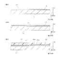
- FIG. 3A shows the preparation process
- FIG. 3B shows the first metal thin film forming step
- FIG. 3C shows the base insulating layer forming step.
- the process following the process shown in FIG. 3C is represented.
- 4A shows a second metal thin film forming step
- FIG. 4B shows a conductor layer forming step
- FIG. 4C shows an etching step
- FIG. 4D shows a cover insulating layer forming step.
- FIG. 7A represents a removal step
- FIG. 7B represents a second metal thin film forming step
- FIG. 7C represents a conductor layer forming step.
- the process following the process shown in FIG. 7C is represented.
- FIG. 8A represents an etching process
- FIG. 8B represents a cover insulating layer forming process.
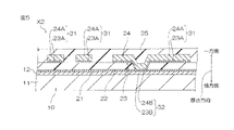
- the wiring circuit board X1 as an embodiment of the wiring circuit board of the present invention includes a metal support substrate 10, a first metal thin film 21, and an insulating layer 22 as a base insulating layer.
- the second metal thin film 23, the conductor layer 24, and the insulating layer 25 as the cover insulating layer are provided in order toward one side in the thickness direction.
- the wiring circuit board X1 extends in a direction (plane direction) orthogonal to the thickness direction and has a predetermined plan view shape.
- the metal support substrate 10 includes a metal support layer 11 and a surface metal layer 12.
- the metal support layer 11 is a base material for ensuring the strength of the wiring circuit board X1.
- Materials for the metal support layer 11 include, for example, stainless steel, copper, copper alloys, aluminum, nickel, titanium, and 42 alloys. Examples of stainless steel include SUS304 based on the AISI (American Iron and Steel Institute) standard. From the viewpoint of the strength of the metal support layer 11, the metal support layer 11 preferably contains at least one selected from the group consisting of stainless steel, copper alloys, aluminum, nickel, and titanium, and more preferably stainless steel. , Copper alloy, aluminum, nickel, and at least one selected from the group consisting of titanium. From the viewpoint of achieving both strength and conductivity of the metal support layer 11, the metal support layer 11 is preferably made of a copper alloy. The thickness of the metal support layer 11 is, for example, 15 ⁇ m or more. The thickness of the metal support layer 11 is, for example, 500 ⁇ m or less, preferably 250 ⁇ m or less.
- the surface metal layer 12 is arranged on one surface in the thickness direction of the metal support layer 11 (the surface metal layer 12 is in contact with the metal support layer 11). In the present embodiment, the surface metal layer 12 is arranged on the entire surface of the metal support layer 11 on one side in the thickness direction.
- the surface metal layer 12 includes, for example, a film formed by a sputtering method (sputtered film), a film formed by a plating method (plating film), and a film formed by a vacuum vapor deposition method (vacuum thin film). Can be mentioned.
- the surface metal layer 12 has a higher conductivity than the metal support layer 11. From the viewpoint of the conductivity of the surface metal layer 12, the surface metal layer 12 preferably contains at least one selected from the group consisting of gold, silver, and copper, more preferably composed of gold, silver, and copper. It consists of at least one selected from the group.
- the surface metal layer 12 is preferably made of copper from the viewpoint of film forming property of the surface metal layer 12 when the metal support layer 11 is made of a copper alloy.
- the thickness of the surface metal layer 12 is preferably 0.5 ⁇ m or more, more preferably 3 ⁇ m or more.
- the first metal thin film 21 is arranged on one side of the metal support substrate 10 in the thickness direction.
- the first metal thin film 21 is arranged on the entire surface of the metal support substrate 10 on one side in the thickness direction.
- the first metal thin film 21 is a layer for ensuring the adhesion of the insulating layer 22 to the metal support substrate 10.
- the first metal thin film 21 includes, for example, a film formed by a sputtering method (sputtered film), a film formed by a plating method (plating film), and a film formed by a vacuum vapor deposition method (vacuum thin film deposition). Membrane).
- Examples of the material of the first metal thin film 21 include chromium, nickel, and titanium.
- the material of the first metal thin film 21 may be an alloy containing two or more metals selected from the group consisting of chromium, nickel, and titanium. Chromium is preferably used as the material of the first metal thin film 21.
- the thickness of the first metal thin film 21 is, for example, 1 nm or more, preferably 10 nm or more, and more preferably 20 nm or more.
- the thickness of the first metal thin film 21 is, for example, 10000 nm or less, preferably 1000 nm or less, and more preferably 500 nm or less.
- the insulating layer 22 is arranged on one surface of the first metal thin film 21 in the thickness direction.
- the material of the insulating layer 22 include resin materials such as polyimide, polyether nitrile, polyether sulfone, polyethylene terephthalate, polyethylene naphthalate, and polyvinyl chloride (the same applies to the material of the insulating layer 25 described later). Resin material can be mentioned).
- the thickness of the insulating layer 22 is, for example, 1 ⁇ m or more, preferably 3 ⁇ m or more.
- the thickness of the insulating layer 22 is, for example, 35 ⁇ m or less.
- the insulating layer 22 has a through hole 22a that penetrates the insulating layer 22 in the thickness direction.
- the through hole 22a has, for example, a substantially circular shape in a plan view.
- the through hole 22a has an inclined inner wall surface 22b in the present embodiment.
- the inner wall surface 22b is inclined so as to be arranged inward toward the portion closer to the metal support substrate 10. That is, the inner wall surface 22b is inclined so that the opening cross-sectional area of the through hole 22a becomes smaller as the portion closer to the metal support substrate 10.
- the first metal thin film 21 has a portion 21a facing the through hole 22a.
- the second metal thin film 23 is formed on one surface of the insulating layer 22 in the thickness direction, on the inner wall surface 22b of the through hole 22a, and on the portion 21a of the first metal thin film 21 facing the through hole 22a. It is arranged continuously.
- the second metal thin film 23 includes a second metal thin film 23A arranged outside the through hole 22a and a second metal thin film 23B arranged inside the through hole 22a.
- the second metal thin film 23B has a concave shape, for example, in the vertical cross section shown in FIG.
- the second metal thin film 23A has a predetermined pattern shape.
- the second metal thin film 23B is connected to the first metal thin film 21.
- the second metal thin film 23A and the second metal thin film 23B are connected to each other.
- the second metal thin film 23 is a seed layer for forming the conductor layer 24.
- Examples of the second metal thin film 23 include a sputter film, a plating film, and a vacuum-deposited film.
- the material of the second metal thin film 23 examples include chromium, copper, nickel, and titanium.
- the material of the second metal thin film 23 may be an alloy containing two or more metals selected from the group consisting of chromium, copper, nickel, and titanium. Chromium is preferably used as the material of the second metal thin film 23.
- the second metal thin film 23 may have a single-layer structure or may have a multi-layer structure of two or more layers. When the second metal thin film 23 has a multilayer structure, the second metal thin film 23 is composed of, for example, a chromium layer as a lower layer and a copper layer on the chromium layer.
- the thickness of the second metal thin film 23 is, for example, 1 nm or more, preferably 10 nm or more.
- the thickness of the second metal thin film 23 is, for example, 500 nm or less, preferably 200 nm or less.
- the conductor layer 24 is arranged on one surface of the second metal thin film 23 in the thickness direction.
- the conductor layer 24 includes a wiring portion 24A arranged outside the through hole 22a and a via portion 24B arranged inside the through hole 22a.
- the wiring portion 24A and the via portion 24B are connected to each other.
- the wiring portion 24A has a predetermined pattern shape.
- the via portion 24B has a concave shape, for example, in the vertical cross section shown in FIG.
- the via portion 24B has an inclined peripheral side surface 24b.
- the peripheral side surface 24b is inclined so as to be arranged inward toward the portion closer to the metal support substrate 10. That is, the peripheral side surface 24b is inclined so that the cross-sectional area of the via portion 24B becomes smaller as the portion closer to the metal support substrate 10.
- Examples of the material of the conductor layer 24 include copper, nickel, and gold.
- the material of the conductor layer 24 may be an alloy containing two or more metals selected from the group consisting of copper, nickel, and gold. Copper is preferably used as the material of the conductor layer 24.
- the second metal thin film 23A and the wiring portion 24A on the second metal thin film 23A form a wiring layer 31 having a predetermined pattern shape.
- the portion 21a of the first metal thin film 21, the second metal thin film 23B, and the via portion 24B on the second metal thin film 23B form the via 32.
- the via 32 is connected to the surface metal layer 12 having a higher conductivity than the metal support layer 11 in the metal support substrate 10.
- the metal support substrate 10 and the wiring layer 31 are electrically connected to each other via the via 32.
- the wiring layer 31 can be ground-connected via the via 32 and the metal support substrate 10.
- the thickness of the wiring layer 31 is, for example, 3 ⁇ m or more, preferably 5 ⁇ m or more.
- the thickness of the wiring layer 31 is, for example, 50 ⁇ m or less, preferably 30 ⁇ m or less.
- the width of the wiring layer 31 (dimensions in the direction orthogonal to the extending direction of the wiring layer 31) is, for example, 5 ⁇ m or more, preferably 8 ⁇ m or more.
- the width of the wiring layer 31 is, for example, 100 ⁇ m or less, preferably 50 ⁇ m or less.
- the insulating layer 25 is arranged so as to cover the wiring layer 31 and the via 32 on one side in the thickness direction of the insulating layer 22.
- the insulating layer 25 may have an opening that partially exposes the wiring layer 31 and / or the via 32. That is, the insulating layer 25 may have an opening, and the wiring layer 31 and / or the via 32 may be exposed at the opening.
- the portion of the wiring layer 31 and / or the via 32 exposed at the opening can function as, for example, a terminal portion of the wiring circuit board X1.
- the thickness of such an insulating layer 25 is, for example, 4 ⁇ m or more, preferably 6 ⁇ m or more.
- the thickness of the insulating layer is, for example, 60 ⁇ m or less, preferably 40 ⁇ m or less.
- 3A to 3C and 4A to 4D show a method of manufacturing a wiring circuit board X1 as an embodiment of the method of manufacturing a wiring circuit board of the present invention.
- 3A to 3C, and 4A to 4D show the manufacturing method as a change in cross section corresponding to FIG.
- the metal support substrate 10 is prepared (preparation step).
- the metal support substrate 10 can be prepared by forming a surface metal layer 12 on the metal support layer 11 as a base material.
- Examples of the method for forming the surface metal layer 12 include a sputtering method, a plating method, and a vacuum vapor deposition method.
- the surface metal layer 12 is preferably formed by a plating method.
- the first metal thin film 21 is formed on the metal support substrate 10 (first metal thin film forming step).
- the method for forming the first metal thin film 21 include a sputtering method, a vacuum vapor deposition method, and a plating method.
- the plating method include an electrolytic plating method and an electroless plating method.
- the first metal thin film 21 is preferably formed by a sputtering method.
- the insulating layer 22 is formed on one surface of the first metal thin film 21 in the thickness direction (base insulating layer forming step).
- the insulating layer 22 is formed, for example, as follows. First, a photosensitive resin solution (varnish) is applied onto the first metal thin film 21 to form a coating film. Next, this coating film is dried by heating. Next, the coating film is subjected to an exposure treatment via a predetermined mask, a subsequent development treatment, and then a baking treatment, if necessary. For example, as described above, the insulating layer 22 having the through holes 22a can be formed on the first metal thin film 21. The portion 21a of the first metal thin film 21 is exposed in the through hole 22a.
- the second metal thin film 23 is formed (second metal thin film forming step).
- the second metal thin film 23 is formed on one surface of the insulating layer 22 in the thickness direction, on the inner wall surface 22b of the through hole 22a, and the portion 21a of the first metal thin film 21 exposed by the through hole 22a.
- the second metal thin film 23 is continuously formed on the top (the second metal thin film 23 includes the second metal thin film 23A outside the through hole 22a and the second metal thin film 23B inside the through hole 22a).
- Examples of the method for forming the second metal thin film 23 include a sputtering method, a vacuum vapor deposition method, and a plating method.
- the plating method include an electrolytic plating method and an electroless plating method.
- the second metal thin film 23 is preferably formed by a sputtering method.
- the conductor layer 24 is formed on one surface of the second metal thin film 23 in the thickness direction (conductor layer forming step). Specifically, for example, it is as follows.
- a resist pattern is formed on the second metal thin film 23.
- the resist pattern has an opening having a shape corresponding to the pattern shape of the conductor layer 24.
- a photosensitive resist film is bonded onto the second metal thin film 23 to form a resist film.
- the resist film is exposed to an exposure process via a predetermined mask, a subsequent development process, and then a bake process, if necessary.
- the above-mentioned metal is then grown on the second metal thin film 23 in the opening of the resist pattern by, for example, an electrolytic plating method.
- the resist pattern is removed.
- the conductor layer 24 having a predetermined pattern can be formed on one surface of the second metal thin film 23 in the thickness direction (the conductor layer 24 is the wiring portion 24A on the second metal thin film 23A and the second one. Including the via portion 24B on the metal thin film 23B).
- the portion of the second metal thin film 23 that is not covered with the conductor layer 24 is removed by etching (etching step).
- etching step As a result, the wiring layer 31 (wiring portion 24A, second metal thin film 23A) and via 32 (via portion 24B, second metal thin film 23B, portion 21a) are formed.
- a nickel film may be formed on the surface of the wiring layer 31 by, for example, an electroless plating method or an electrolytic plating method.
- the insulating layer 25 is formed on the insulating layer 22 so as to cover the wiring layer 31 and the via 32 (cover insulating layer forming step).
- the insulating layer 25 is formed, for example, as follows. First, a photosensitive resin solution (varnish) is applied on the insulating layer 22, the wiring layer 31, and the via 32 to form a coating film. Next, this coating film is dried. Next, the coating film is subjected to an exposure treatment via a predetermined mask, a subsequent development treatment, and then a baking treatment, if necessary. For example, as described above, the insulating layer 25 as the cover insulating layer can be formed.
- the metal support substrate 10 is then patterned by etching the metal support substrate 10.
- This pattern processing includes, for example, processing for forming the outer shape (outer shape in a plan view) of the metal support substrate 10 and processing for forming, for example, an island portion separated from the surroundings in the metal support substrate 10.
- a gold plating film may be formed on the exposed surface of the metal support substrate 10 by an electrolytic plating method or an electroless plating method.
- the exposed surface of the metal support substrate 10 includes a surface that is not covered by the insulating layer 25 on one surface (surface metal layer 12) in the thickness direction of the metal support substrate 10, a side surface of the metal support substrate 10, and a side surface of the metal support substrate 10. , The other side of the metal support substrate 10 in the thickness direction (lower surface in the figure) is included.
- the wiring circuit board X1 can be manufactured.
- the metal support substrate 10 is arranged on the metal support layer 11 and one surface of the metal support layer 11 in the thickness direction, and has a higher conductivity than the metal support layer 11.
- a metal layer 12 is provided.
- the via 32 is connected to the surface metal layer 12 having a higher conductivity than the metal support layer 11 in the metal support substrate 10. Therefore, the wiring circuit board X1 is suitable for realizing a low resistance electrical connection between the wiring layer 31 arranged on one side in the thickness direction of the metal support board 10 and the metal support board 10.
- the surface metal layer 12 having a higher conductivity than the metal support layer 11 is arranged on one surface of the metal support layer 11 in the thickness direction.
- the structure in which the metal support layer 11 and the surface metal layer 12 are in direct contact with each other without interposing another layer such as a Cr layer as a plating seed layer is such that the metal support substrate 10 is subjected to a single treatment with respect to the metal support substrate 10. Suitable for efficient pattern processing.
- the wiring circuit board X1 realizes a low resistance electrical connection between the metal support substrate 10 and the wiring layer 31 formed on the insulating layer 22 on the metal support substrate 10. It is suitable for efficiently patterning the metal support substrate 10.
- the wiring circuit board X2 includes a metal support substrate 10, a first metal thin film 21, an insulating layer 22 as a base insulating layer, a second metal thin film 23, a conductor layer 24, and an insulating layer 25 as a cover insulating layer. Are prepared in order toward one side in the thickness direction.
- the first metal thin film 21 has an opening 21b
- the second metal thin film 23 is connected to the first metal thin film 21 at the opening 21b.
- the wiring circuit board X2 has the same configuration as the wiring circuit board X1.
- the opening 21b of the first metal thin film 21 penetrates the first metal thin film 21 in the thickness direction.
- the opening 21b has, for example, a substantially circular shape in a plan view.
- the opening 21b is opened along the through hole 22a of the insulating layer 22. That is, the through hole 22a and the opening 21b overlap each other in a plan view.
- the through hole 22a and the opening 21b form a through hole H.
- the second metal thin film 23 is continuously arranged on one surface of the insulating layer 22 in the thickness direction and on the portion 10a of the metal support board 10 facing the through hole H ().
- the second metal thin film 23 includes the second metal thin film 23A outside the through hole H and the second metal thin film 23B inside the through hole H).
- the second metal thin film 23B is directly connected to the metal support substrate 10.
- the second metal thin film 23B and the via portion 24B on the second metal thin film 23B form the via 32 in the through hole H.
- the via 32 is connected to the surface metal layer 12 having a higher conductivity than the metal support layer 11 in the metal support substrate 10.
- the metal support substrate 10 and the wiring layer 31 are electrically connected to each other via the via 32.
- the wiring layer 31 can be ground-connected via the via 32 and the metal support substrate 10.
- FIGS. 8A to 8B represent a part of the steps in the method for manufacturing the wiring circuit board X2 as an embodiment of the method for manufacturing the wiring circuit board of the present invention.
- 7A to 7C, and 8A to 8B show this manufacturing method as a change in cross section corresponding to FIG.
- first, the preparation step, the first metal thin film forming step, and the base insulating layer forming step are carried out in the same manner as described above with reference to FIGS. 3A to 3C.
- the portion 21a of the first metal thin film 21 exposed in the through hole 22a of the insulating layer 22 is removed.
- a part (part 10a) of the metal support substrate 10 is exposed through the through hole 22a (removal step).
- the opening 21b is formed by removing the portion 21a (the opening 21b is opened along the through hole 22a, and the opening H is formed by the through hole 22a and the opening 21b. Is formed).
- Examples of the removal method in this step include wet etching and dry etching, and wet etching is preferable.
- Examples of the etching solution for wet etching include a dicerium nitrate solution, an aqueous solution of caustic soda, a potassium permanganate solution, and a sodium metasilicate solution, and a dicerium ammonium nitrate solution is preferably used. ..
- the temperature of the etching solution in the wet etching is, for example, 20 ° C. or higher, preferably 30 ° C. or higher.
- the etching solution temperature is, for example, 80 ° C. or lower, preferably 65 ° C. or lower.
- the etching time (immersion time) in the wet etching is, for example, 1 minute or more.
- the etching time is, for example, 15 minutes or less, preferably 10 minutes or less.
- the second metal thin film 23 is formed (second metal thin film forming step).
- the second metal thin film 23 is continuously formed on one surface of the insulating layer 22 in the thickness direction and on the portion 10a of the metal support substrate 10 exposed by the through hole H.
- the second metal thin film 23 includes the second metal thin film 23A outside the through hole 22a and the second metal thin film 23B inside the through hole 22a).
- Examples of the method for forming the second metal thin film 23 include a sputtering method, a vacuum vapor deposition method, and a plating method.
- the plating method include an electrolytic plating method and an electroless plating method.
- the second metal thin film 23 is preferably formed by a sputtering method.
- the conductor layer 24 is formed on one surface of the second metal thin film 23 in the thickness direction (conductor layer forming step). Specifically, it is the same as the conductor forming step described above with reference to FIG. 4B.
- the portion of the second metal thin film 23 that is not covered with the conductor layer 24 is removed by etching (etching step).
- etching step As a result, the wiring layer 31 (wiring portion 24A, second metal thin film 23A) and via 32 (via portion 24B, second metal thin film 23B) are formed.
- the insulating layer 25 is formed on the insulating layer 22 so as to cover the wiring layer 31 and the via 32 (cover insulating layer forming step). Specifically, it is the same as the cover insulating layer forming step described above with reference to FIG. 4D.
- the metal support substrate 10 is then patterned by etching the metal support substrate 10.
- This pattern processing includes, for example, processing for forming the outer shape (outer shape in a plan view) of the metal support substrate 10 and processing for forming, for example, an island portion separated from the surroundings in the metal support substrate 10.
- the wiring circuit board X2 can be manufactured.
- a removal step (shown in FIG. 7A) is carried out after the base insulating layer forming step (shown in FIG. 3C).
- the removing step the portion 21a of the first metal thin film 21 is removed, and the metal support substrate 10 is exposed in the through hole 22a.
- the portion 21a with an oxide film is removed. can.
- the second metal thin film 23B is formed on the portion 10a of the metal supporting substrate 10 facing the through hole 22a.
- the via portion 24B is formed on the second metal thin film 23B.
- the via 32 (second metal thin film 23B, via portion 24B) is formed in the through hole 22a.
- the via 32 connected to the metal support substrate 10 is formed without passing through the first metal thin film 21. Therefore, this manufacturing method is suitable for realizing a low resistance electrical connection between the metal support substrate 10 and the wiring layer 31.
- the metal support substrate 10 is arranged on one side of the metal support layer 11 in the thickness direction, and the surface metal layer 12 having a higher conductivity than the metal support layer 11 is provided. Be prepared. Further, the via 32 is connected to the surface metal layer 12 having a higher conductivity than the metal support layer 11 in the metal support substrate 10. Therefore, the wiring circuit board X2 is suitable for realizing a low resistance electrical connection between the metal support board 10 and the wiring layer 31, like the wiring circuit board X1, and the metal support board 10 is efficiently connected. Suitable for pattern processing.
- the wiring circuit board of the present invention can be applied to a wiring circuit board provided with a metal support board as a support base material.
Landscapes
- Engineering & Computer Science (AREA)
- Microelectronics & Electronic Packaging (AREA)
- Manufacturing & Machinery (AREA)
- Chemical & Material Sciences (AREA)
- Dispersion Chemistry (AREA)
- Production Of Multi-Layered Print Wiring Board (AREA)
- Printing Elements For Providing Electric Connections Between Printed Circuits (AREA)
- Insulated Metal Substrates For Printed Circuits (AREA)
Priority Applications (3)
| Application Number | Priority Date | Filing Date | Title |
|---|---|---|---|
| US18/252,308 US20240015884A1 (en) | 2020-11-13 | 2021-10-28 | Wiring circuit board and method for producing wiring circuit board |
| KR1020237015106A KR20230106601A (ko) | 2020-11-13 | 2021-10-28 | 배선 회로 기판, 및 배선 회로 기판의 제조 방법 |
| CN202180075586.6A CN116420431A (zh) | 2020-11-13 | 2021-10-28 | 布线电路基板和布线电路基板的制造方法 |
Applications Claiming Priority (2)
| Application Number | Priority Date | Filing Date | Title |
|---|---|---|---|
| JP2020189117A JP7289602B2 (ja) | 2020-11-13 | 2020-11-13 | 配線回路基板、および配線回路基板の製造方法 |
| JP2020-189117 | 2020-11-13 |
Publications (1)
| Publication Number | Publication Date |
|---|---|
| WO2022102416A1 true WO2022102416A1 (ja) | 2022-05-19 |
Family
ID=81601082
Family Applications (1)
| Application Number | Title | Priority Date | Filing Date |
|---|---|---|---|
| PCT/JP2021/039762 WO2022102416A1 (ja) | 2020-11-13 | 2021-10-28 | 配線回路基板、および配線回路基板の製造方法 |
Country Status (6)
Cited By (1)
| Publication number | Priority date | Publication date | Assignee | Title |
|---|---|---|---|---|
| CN119364644A (zh) * | 2024-12-24 | 2025-01-24 | 深圳市鑫荣进绝缘材料有限公司 | 铝基电路板制作方法及铝基电路板 |
Families Citing this family (1)
| Publication number | Priority date | Publication date | Assignee | Title |
|---|---|---|---|---|
| JP2023066606A (ja) * | 2021-10-29 | 2023-05-16 | 日東電工株式会社 | 配線回路基板およびその製造方法 |
Citations (5)
| Publication number | Priority date | Publication date | Assignee | Title |
|---|---|---|---|---|
| JPH0258899A (ja) * | 1988-08-25 | 1990-02-28 | Matsushita Electric Works Ltd | プリント配線板 |
| JPH03133633A (ja) * | 1989-10-20 | 1991-06-06 | Nippon Steel Corp | 鉄系プリント基板に適した鋼板 |
| JP2000309887A (ja) * | 1999-02-23 | 2000-11-07 | Mitsui Chemicals Inc | クロメート系防錆膜の除去方法および配線基板の製造方法 |
| JP2012222047A (ja) * | 2011-04-05 | 2012-11-12 | Sumitomo Electric Ind Ltd | プリント配線板およびそのプリント配線板の製造方法 |
| JP2016045971A (ja) * | 2014-08-21 | 2016-04-04 | 日東電工株式会社 | 回路付サスペンション基板の製造方法 |
Family Cites Families (4)
| Publication number | Priority date | Publication date | Assignee | Title |
|---|---|---|---|---|
| JPH01169990A (ja) * | 1987-12-24 | 1989-07-05 | Hitachi Cable Ltd | 表面実装用基板 |
| JP4615427B2 (ja) | 2005-12-01 | 2011-01-19 | 日東電工株式会社 | 配線回路基板 |
| JP7085328B2 (ja) * | 2017-09-29 | 2022-06-16 | 日東電工株式会社 | 配線回路基板、その製造方法および撮像装置 |
| JP7066528B2 (ja) * | 2018-05-31 | 2022-05-13 | 日東電工株式会社 | 配線回路基板、その製造方法および配線回路シート |
-
2020
- 2020-11-13 JP JP2020189117A patent/JP7289602B2/ja active Active
-
2021
- 2021-10-28 US US18/252,308 patent/US20240015884A1/en active Pending
- 2021-10-28 KR KR1020237015106A patent/KR20230106601A/ko active Pending
- 2021-10-28 WO PCT/JP2021/039762 patent/WO2022102416A1/ja active Application Filing
- 2021-10-28 CN CN202180075586.6A patent/CN116420431A/zh active Pending
- 2021-11-05 TW TW110141331A patent/TW202226908A/zh unknown
-
2023
- 2023-03-08 JP JP2023035442A patent/JP7538912B2/ja active Active
Patent Citations (5)
| Publication number | Priority date | Publication date | Assignee | Title |
|---|---|---|---|---|
| JPH0258899A (ja) * | 1988-08-25 | 1990-02-28 | Matsushita Electric Works Ltd | プリント配線板 |
| JPH03133633A (ja) * | 1989-10-20 | 1991-06-06 | Nippon Steel Corp | 鉄系プリント基板に適した鋼板 |
| JP2000309887A (ja) * | 1999-02-23 | 2000-11-07 | Mitsui Chemicals Inc | クロメート系防錆膜の除去方法および配線基板の製造方法 |
| JP2012222047A (ja) * | 2011-04-05 | 2012-11-12 | Sumitomo Electric Ind Ltd | プリント配線板およびそのプリント配線板の製造方法 |
| JP2016045971A (ja) * | 2014-08-21 | 2016-04-04 | 日東電工株式会社 | 回路付サスペンション基板の製造方法 |
Cited By (1)
| Publication number | Priority date | Publication date | Assignee | Title |
|---|---|---|---|---|
| CN119364644A (zh) * | 2024-12-24 | 2025-01-24 | 深圳市鑫荣进绝缘材料有限公司 | 铝基电路板制作方法及铝基电路板 |
Also Published As
| Publication number | Publication date |
|---|---|
| US20240015884A1 (en) | 2024-01-11 |
| CN116420431A (zh) | 2023-07-11 |
| JP2022078438A (ja) | 2022-05-25 |
| JP7289602B2 (ja) | 2023-06-12 |
| KR20230106601A (ko) | 2023-07-13 |
| JP2023073270A (ja) | 2023-05-25 |
| JP7538912B2 (ja) | 2024-08-22 |
| TW202226908A (zh) | 2022-07-01 |
Similar Documents
| Publication | Publication Date | Title |
|---|---|---|
| JP7538912B2 (ja) | 配線回路基板、および配線回路基板の製造方法 | |
| US6803528B1 (en) | Multi-layer double-sided wiring board and method of fabricating the same | |
| WO2022030074A1 (ja) | 配線回路基板の製造方法、および配線回路基板 | |
| JP2003152340A (ja) | 多層配線基板の製造方法 | |
| TW201117684A (en) | Printed circuit board structure and method for manufacturing the same | |
| WO2020241645A1 (ja) | 多層配線基板及びその製造方法 | |
| TW202332345A (zh) | 配線電路基板及其製造方法 | |
| KR102823140B1 (ko) | 양면 배선 회로 기판의 제조 방법 및 양면 배선 회로 기판 | |
| JPH05335713A (ja) | 片側閉塞微小スルホール付きプリント基板用積層板、およびそのプリント基板用積層板への導通メッキ方法 | |
| WO2021261178A1 (ja) | 配線回路基板集合体シートおよびその製造方法 | |
| JP2013110408A (ja) | 印刷回路基板及びその製造方法 | |
| JP2004014975A (ja) | 金属箔付フレキシブル回路基板 | |
| WO2001035704A1 (en) | Multi-layer double-sided wiring board and method of fabricating the same | |
| WO2020230470A1 (ja) | 配線回路基板 | |
| WO2022113649A1 (ja) | 配線回路基板 | |
| WO2021256208A1 (ja) | 配線回路基板 | |
| JPH02228092A (ja) | 両面配線基板の製造方法 | |
| JP2003273170A (ja) | 両面配線テープキャリアの製造方法並びにこれを用いたテープキャリア | |
| JPH06334335A (ja) | スルーホールメッキ法 | |
| KR20240043099A (ko) | 배선 회로 기판의 제조 방법 | |
| JPH10335826A (ja) | 多層配線回路基板及びその製造方法 | |
| KR20230160259A (ko) | 배선 회로 기판의 제조 방법 | |
| JP2000252633A (ja) | 多層配線基板の製造方法 | |
| JP2001217541A (ja) | 多層型プリント配線基板及び多層型プリント配線基板の製造方法 |
Legal Events
| Date | Code | Title | Description |
|---|---|---|---|
| 121 | Ep: the epo has been informed by wipo that ep was designated in this application |
Ref document number: 21891663 Country of ref document: EP Kind code of ref document: A1 |
|
| WWE | Wipo information: entry into national phase |
Ref document number: 18252308 Country of ref document: US |
|
| NENP | Non-entry into the national phase |
Ref country code: DE |
|
| 122 | Ep: pct application non-entry in european phase |
Ref document number: 21891663 Country of ref document: EP Kind code of ref document: A1 |