WO2022085552A1 - 積層型コイル部品 - Google Patents
積層型コイル部品 Download PDFInfo
- Publication number
- WO2022085552A1 WO2022085552A1 PCT/JP2021/038011 JP2021038011W WO2022085552A1 WO 2022085552 A1 WO2022085552 A1 WO 2022085552A1 JP 2021038011 W JP2021038011 W JP 2021038011W WO 2022085552 A1 WO2022085552 A1 WO 2022085552A1
- Authority
- WO
- WIPO (PCT)
- Prior art keywords
- conductor
- coil
- width
- coil conductor
- laminated
- Prior art date
- Legal status (The legal status is an assumption and is not a legal conclusion. Google has not performed a legal analysis and makes no representation as to the accuracy of the status listed.)
- Ceased
Links
Images


Classifications
-
- H—ELECTRICITY
- H01—ELECTRIC ELEMENTS
- H01F—MAGNETS; INDUCTANCES; TRANSFORMERS; SELECTION OF MATERIALS FOR THEIR MAGNETIC PROPERTIES
- H01F27/00—Details of transformers or inductances, in general
- H01F27/28—Coils; Windings; Conductive connections
- H01F27/2804—Printed windings
-
- H—ELECTRICITY
- H01—ELECTRIC ELEMENTS
- H01F—MAGNETS; INDUCTANCES; TRANSFORMERS; SELECTION OF MATERIALS FOR THEIR MAGNETIC PROPERTIES
- H01F17/00—Fixed inductances of the signal type
- H01F17/0006—Printed inductances
- H01F17/0013—Printed inductances with stacked layers
-
- H—ELECTRICITY
- H01—ELECTRIC ELEMENTS
- H01F—MAGNETS; INDUCTANCES; TRANSFORMERS; SELECTION OF MATERIALS FOR THEIR MAGNETIC PROPERTIES
- H01F27/00—Details of transformers or inductances, in general
- H01F27/28—Coils; Windings; Conductive connections
- H01F27/29—Terminals; Tapping arrangements for signal inductances
- H01F27/292—Surface mounted devices
-
- H—ELECTRICITY
- H01—ELECTRIC ELEMENTS
- H01F—MAGNETS; INDUCTANCES; TRANSFORMERS; SELECTION OF MATERIALS FOR THEIR MAGNETIC PROPERTIES
- H01F27/00—Details of transformers or inductances, in general
- H01F27/28—Coils; Windings; Conductive connections
- H01F27/32—Insulating of coils, windings, or parts thereof
- H01F27/323—Insulation between winding turns, between winding layers
-
- H—ELECTRICITY
- H01—ELECTRIC ELEMENTS
- H01F—MAGNETS; INDUCTANCES; TRANSFORMERS; SELECTION OF MATERIALS FOR THEIR MAGNETIC PROPERTIES
- H01F17/00—Fixed inductances of the signal type
- H01F17/0006—Printed inductances
- H01F17/0013—Printed inductances with stacked layers
- H01F2017/002—Details of via holes for interconnecting the layers
-
- H—ELECTRICITY
- H01—ELECTRIC ELEMENTS
- H01F—MAGNETS; INDUCTANCES; TRANSFORMERS; SELECTION OF MATERIALS FOR THEIR MAGNETIC PROPERTIES
- H01F17/00—Fixed inductances of the signal type
- H01F17/04—Fixed inductances of the signal type with magnetic core
- H01F2017/048—Fixed inductances of the signal type with magnetic core with encapsulating core, e.g. made of resin and magnetic powder
-
- H—ELECTRICITY
- H01—ELECTRIC ELEMENTS
- H01F—MAGNETS; INDUCTANCES; TRANSFORMERS; SELECTION OF MATERIALS FOR THEIR MAGNETIC PROPERTIES
- H01F27/00—Details of transformers or inductances, in general
- H01F27/28—Coils; Windings; Conductive connections
- H01F27/2804—Printed windings
- H01F2027/2809—Printed windings on stacked layers
-
- H—ELECTRICITY
- H01—ELECTRIC ELEMENTS
- H01F—MAGNETS; INDUCTANCES; TRANSFORMERS; SELECTION OF MATERIALS FOR THEIR MAGNETIC PROPERTIES
- H01F41/00—Apparatus or processes specially adapted for manufacturing or assembling magnets, inductances or transformers; Apparatus or processes specially adapted for manufacturing materials characterised by their magnetic properties
- H01F41/02—Apparatus or processes specially adapted for manufacturing or assembling magnets, inductances or transformers; Apparatus or processes specially adapted for manufacturing materials characterised by their magnetic properties for manufacturing cores, coils, or magnets
- H01F41/04—Apparatus or processes specially adapted for manufacturing or assembling magnets, inductances or transformers; Apparatus or processes specially adapted for manufacturing materials characterised by their magnetic properties for manufacturing cores, coils, or magnets for manufacturing coils
- H01F41/041—Printed circuit coils
-
- H—ELECTRICITY
- H01—ELECTRIC ELEMENTS
- H01F—MAGNETS; INDUCTANCES; TRANSFORMERS; SELECTION OF MATERIALS FOR THEIR MAGNETIC PROPERTIES
- H01F41/00—Apparatus or processes specially adapted for manufacturing or assembling magnets, inductances or transformers; Apparatus or processes specially adapted for manufacturing materials characterised by their magnetic properties
- H01F41/02—Apparatus or processes specially adapted for manufacturing or assembling magnets, inductances or transformers; Apparatus or processes specially adapted for manufacturing materials characterised by their magnetic properties for manufacturing cores, coils, or magnets
- H01F41/04—Apparatus or processes specially adapted for manufacturing or assembling magnets, inductances or transformers; Apparatus or processes specially adapted for manufacturing materials characterised by their magnetic properties for manufacturing cores, coils, or magnets for manufacturing coils
- H01F41/12—Insulating of windings
- H01F41/122—Insulating between turns or between winding layers
-
- H—ELECTRICITY
- H03—ELECTRONIC CIRCUITRY
- H03H—IMPEDANCE NETWORKS, e.g. RESONANT CIRCUITS; RESONATORS
- H03H7/00—Multiple-port networks comprising only passive electrical elements as network components
Definitions
- the present invention relates to a laminated coil component.
- Patent Document 1 discloses a laminated coil component containing a coil inside an insulating prime field having a laminated structure, in which adjacent coil portions are connected by a layered connecting portion.
- the connecting portion is arranged at a position corresponding to the position of the divided portion of the coil portion, and has a rectangular shape extending along the shape of the divided portion. Further, Patent Document 1 shows a structure in which the thicknesses of the upper coil layer and the lower coil layer of the connecting portion in the stacking direction are different. Patent Document 1 states that it is possible to provide a laminated coil component in which the number of types of coil portions constituting the coil is reduced.
- connection part of the laminated coil component is made of a conductor containing a metal such as silver, and an insulating layer made of an insulating material such as ferrite exists around the connection part.
- thermal stress generated by the difference in linear expansion coefficient between the conductor and the insulating material at the connection portion during the heat treatment in the process of processing the laminated coil component, especially in the temperature lowering process in which the temperature changes from high temperature to low temperature. Concentrate. Specifically, tensile stress is generated in the insulating layer when the conductor contracts. If the tensile stress is larger than the strength of the insulating layer, cracks may occur in the insulating layer around the connection portion.
- the present invention has been made to solve the above problems, and an object of the present invention is to provide a laminated coil component in which cracks are unlikely to occur around a connecting conductor connecting the coil conductors.
- the laminated coil component of the present invention has a laminated body in which a plurality of insulating layers are laminated and has a built-in coil, and an external surface provided on the outer surface of the laminated body and electrically connected to the coil.
- the conductor width of the connecting conductor is smaller than the conductor width of the first coil conductor, and the second coil conductor is described.
- the conductor width of the coil conductor is smaller than the conductor width of the first coil conductor.
- FIG. 1 is a perspective view schematically showing an example of a laminated coil component of the present invention.
- FIG. 2 is a schematic view schematically showing the laminated coil component of the present invention through the inside so that the structure of the coil can be understood.
- FIG. 3 is a sectional view taken along line AA of FIG. 2, schematically showing the details of the connection portion.
- FIG. 4 is a cross-sectional view schematically showing another example of the connecting portion.
- FIG. 5 is an exploded view schematically showing a method for producing a laminated body by a printing laminating method.
- the laminated coil component of the present invention will be described.
- the present invention is not limited to the following configurations and embodiments, and can be appropriately modified and applied without changing the gist of the present invention. It should be noted that a combination of two or more of the individual preferred configurations and embodiments of the present invention described below is also the present invention.
- FIG. 1 is a perspective view schematically showing an example of a laminated coil component of the present invention.
- FIG. 2 is a schematic view schematically showing the laminated coil component of the present invention through the inside so that the structure of the coil can be understood.
- the laminated coil component 1 shown in FIG. 1 includes a laminated body 10, a first external electrode 21, and a second external electrode 22.
- the laminated body 10 has a substantially rectangular parallelepiped shape having six faces. Although the configuration of the laminated body 10 will be described later, a plurality of insulating layers are laminated and a coil is built in the laminated body 10.
- the first external electrode 21 and the second external electrode 22 are each electrically connected to the coil.
- the direction in which the first external electrode and the second external electrode face each other is defined as the length direction.
- the direction orthogonal to the length direction is defined as the height direction
- the direction orthogonal to the length direction and the height direction is defined as the width direction.
- 1 and 2 show the length direction, the width direction, and the height direction of the laminated coil component and the laminated body as the double-headed arrow L direction, W direction, and T direction, respectively.
- the length direction (L direction), the width direction (W direction), and the height direction (T direction) are orthogonal to each other.
- the mounting surface of the laminated coil component 1 is a surface (LW surface) parallel to the length direction and the width direction.
- the laminate 10 shown in FIGS. 1 and 2 has a first end surface 11 and a second end surface 12 facing in the length direction, and a first main surface 13 and a first main surface 13 facing in the height direction orthogonal to the length direction. It has a second main surface 14 and a first side surface 15 and a second side surface 16 facing each other in the width direction orthogonal to the length direction and the height direction.
- the laminated body 10 has rounded corners and ridges.
- the corner portion is a portion where the three surfaces of the laminated body intersect, and the ridge portion is a portion where the two surfaces of the laminated body intersect.
- the first external electrode 21 covers the first end surface 11 of the laminated body 10 and extends from the first end surface 11 to be a part of the first main surface 13 and the second main surface. It is arranged so as to cover a part of the surface 14, a part of the first side surface 15, and a part of the second side surface 16.
- the second external electrode 22 covers the second end surface 12 of the laminated body 10, extends from the second end surface 12, and is a part of the first main surface 13, the second. It is arranged so as to cover a part of the main surface 14, a part of the first side surface 15, and a part of the second side surface 16.
- the second main surface 14 is the mounting surface.
- the coil is formed by electrically connecting a plurality of coil conductors laminated together with an insulating layer.
- the stacking direction of the laminated body which is the direction in which the plurality of insulating layers are laminated, is along the height direction. Further, the coil axis of the coil is along the height direction.
- the coil conductor and the first external electrode are electrically connected at the first end face, and the coil conductor and the second external electrode are electrically connected at the second end face.
- the coil conductor constituting the coil 30 and the first external electrode 21 are electrically connected by the first end surface 11, and the coil conductor and the second external electrode 22 are electrically connected by the second end surface 12. It shows how it is connected to.
- the conductor that draws the coil 30 to the first end surface 11 is the extraction conductor 35
- the conductor that draws the coil 30 to the second end surface 12 is the extraction conductor 36.
- the connection position between the coil conductor and the external electrode can be changed by changing the position where the coil conductor is pulled out to the outside of the laminate. The drawing position may be changed so that the coil conductor and the external electrode are electrically connected on the main surface or the side surface of the laminated body.
- FIG. 2 shows that adjacent coil conductors are connected via a connecting conductor.
- the adjacent coil conductor connected via the connecting conductor 33 is the first coil conductor 31 or the second coil conductor 32.
- the portion where the first coil conductor 31 and the second coil conductor 32, which are adjacent coil conductors, are connected via the connecting conductor 33 is referred to as a connecting portion 34. That is, the connecting portion is a portion where the first coil conductor comes into contact with the connecting conductor, a portion where the second coil conductor comes into contact with the connecting conductor, and a portion composed of the connecting conductor.
- the conductor width of the connecting conductor 33 is smaller than the conductor width of the first coil conductor 31, and the conductor width of the second coil conductor 32 is the conductor of the first coil conductor 31. Smaller than the width.
- the coil conductor located on the lower side in the height direction is the first coil conductor 31, and the coil located on the upper side in the height direction.
- the conductor is the second coil conductor 32.
- the coil conductor located on the lower side in the height direction is the first coil conductor 31, and the coil conductor located on the upper side in the height direction is the second coil conductor 32. ..
- one coil conductor connected via the connecting conductor 33 becomes the first coil conductor 31, and the other coil conductor becomes the second coil conductor 32. Comparing the conductor width of the connecting conductor, the conductor width of one coil conductor, and the conductor width of the other coil conductor, the coil conductor with the larger conductor width is the first coil conductor, and the coil conductor with the smaller conductor width. Is the second coil conductor. Then, the conductor width of the first coil conductor becomes larger than the conductor width of the connecting conductor. In the connection portion 34 shown in FIG. 2, the first coil conductor 31 is located below and the second coil conductor 32 is located above, but whether it is the first coil conductor or the second coil conductor depends on the conductor width. It is determined, not up and down with respect to the height direction (stacking direction).
- FIG. 3 is a sectional view taken along line AA of FIG. 2, schematically showing the details of the connection portion.
- FIG. 3 shows the first coil conductor 31, the second coil conductor 32, and the connecting conductor 33 constituting the connecting portion 34.
- the conductor width of the first coil conductor 31 is the width indicated by the double-headed arrow W1
- the conductor width of the second coil conductor 32 is the width indicated by the double-headed arrow W2
- the conductor width of the connecting conductor 33 is the width indicated by the double-headed arrow W3.
- the width of each conductor is defined as the width at which the conductor width is the widest.
- the conductor width of the connecting conductor 33 is smaller than the conductor width of the first coil conductor 31, and the conductor width of the second coil conductor 32 is smaller than the conductor width of the first coil conductor 31.
- W3 ⁇ W1 and W2 ⁇ W1 in FIG. 3 the conductor width W3 of the connecting conductor 33 and the conductor width W2 of the second coil conductor 32 are the same, but the conductor width W3 of the connecting conductor 33 and the conductor width W2 of the second coil conductor 32 are the same. It may be different.
- the heat treatment when processing the laminated coil component causes stress in the insulating layer made of an insulating material such as ferrite. This is because the coefficient of linear expansion of a metal such as silver constituting the conductor portion and an insulating material such as ferrite are different.
- a metal such as silver constituting the conductor portion and an insulating material such as ferrite are different.
- tensile stress is generated in the insulating layer when the conductor contracts.
- the larger the displacement of the conductor the larger the tensile stress.
- the tensile stress becomes larger than the strength of the insulating layer, cracks occur in the insulating layer.
- the conductor width of one coil conductor (second coil conductor) smaller than the conductor width of the other coil conductor (first coil conductor)
- the amount of displacement of the conductor is small. Since the tensile stress generated in the insulating layer is reduced, the occurrence of cracks can be prevented.
- the conductor width of the first coil conductor is preferably 180 ⁇ m or more and 380 ⁇ m or less. Further, the conductor width of the first coil conductor other than the connecting portion is preferably the same as the conductor width in the connecting portion, and is preferably 180 ⁇ m or more and 380 ⁇ m or less.
- the conductor width of the second coil conductor is smaller than the conductor width of the first coil conductor, and the conductor width of the second coil conductor is 30% or more and 90% or less of the conductor width of the first coil conductor. Is preferable.
- the conductor width of the second coil conductor is set to 90 of the conductor width of the first coil conductor in consideration of the manufacturing tolerance and the like. It is preferable to set it to% or less.
- the conductor width of the second coil conductor is smaller than 30% of the conductor width of the first coil conductor, the conductor width of the second coil conductor may become too small and the second coil conductor may be disconnected. Further, it is preferable that the difference between the conductor width of the second coil conductor and the conductor width of the first coil conductor is 40 ⁇ m or more and 200 ⁇ m or less. From these viewpoints, the conductor width of the second coil conductor is preferably 55 ⁇ m or more and 340 ⁇ m or less.
- the conductor width of the second coil conductor other than the connecting portion is preferably larger than the conductor width of the second coil conductor at the connecting portion, and is preferably 180 ⁇ m or more and 380 ⁇ m or less. Except for the connection portion, the conductor width of the first coil conductor and the conductor width of the second coil conductor may be the same, and the conductor width of the second coil conductor may be larger than the conductor width of the first coil conductor.
- the conductor thickness of the first coil conductor is preferably 20 ⁇ m or more at the connecting portion. Further, the conductor thickness of the second coil conductor is preferably 20 ⁇ m or more at the connecting portion.
- the conductor thickness of the coil conductor is 20 ⁇ m or more and is thick, cracks tend to occur at the connection portion.
- the width of the coil conductor and the connection conductor at the connection portion has a predetermined relationship. Therefore, it is possible to prevent cracks from occurring at the connection portion even if the coil conductor is thick.
- the conductor width of the connecting conductor is smaller than the conductor width of the first coil conductor, and the conductor width of the connecting conductor is preferably 30% or more and 90% or less of the conductor width of the first coil conductor.
- the conductor width of the connecting conductor is set to 90% or less of the conductor width of the first coil conductor in consideration of the manufacturing tolerance and the like. It is preferable to do so. Further, if the conductor width of the connecting conductor is smaller than 30% of the conductor width of the first coil conductor, the conductor width of the connecting conductor may become too small and the connecting conductor may be broken.
- the difference between the conductor width of the connecting conductor and the conductor width of the first coil conductor is 40 ⁇ m or more and 200 ⁇ m or less.
- the conductor width of the connecting conductor is preferably 55 ⁇ m or more and 340 ⁇ m or less.
- the protruding width of the first coil conductor 31 projecting with respect to the second coil conductor 32 and the connecting conductor 33 is indicated by the double-headed arrow w.
- the first coil conductor 31 protrudes from both the left and right sides of the second coil conductor 32 and the connecting conductor 33.
- the preferable relationship between the width of the first coil conductor and the protrusion width w is, for example, as follows.
- the width of the first coil conductor is 200 ⁇ m or more and less than 300 ⁇ m
- the protrusion width is 20 ⁇ m or more and 80 ⁇ m or less.
- the protrusion width is 40 ⁇ m or more and 100 ⁇ m or less.
- the first coil conductor, the second coil conductor, and the connecting conductor preferably contain a metal, preferably copper, silver, and the like, and more preferably silver.
- a magnetic material or a non-magnetic material can be used as the material of the insulating layer.
- a magnetic ferrite material can be used as the magnetic material. Fe is converted to Fe 2 O 3 and is 40 mol% or more and 49.5 mol% or less, Zn is converted to ZnO and is 5 mol% or more and 35 mol% or less, and Cu is converted to CuO and is 4 mol% or more and 12 mol% or less.
- a magnetic ferrite material having a balance of NiO can be preferably used.
- the above magnetic ferrite material may contain trace additives (including unavoidable impurities) such as Mn, Co, Sn, Bi, and Si.
- a non-magnetic ferrite material As the non-magnetic material, a non-magnetic ferrite material can be used. It is preferable to use a non-magnetic ferrite material in which Fe is 40 mol% or more and 49.5 mol% or less in terms of Fe 2 O 3 , and Cu is 4 mol% or more and 12 mol% or less in terms of CuO, and the balance is ZnO. can.
- the above non-magnetic ferrite material may contain trace additives (including unavoidable impurities) such as Mn, Co, Sn, Bi, and Si.
- the insulating layer includes an insulating layer located at the same height as the first coil conductor, an insulating layer located at the same height as the second coil conductor, and an insulating layer located at the same height as the connecting conductor.
- the insulating layer located at the same height as the connecting conductor includes an insulating layer located between the first coil conductor and the second coil conductor, and an insulating layer located between the first coil conductor and the second coil conductor. There is an insulating layer around.
- the insulating layer located between the first coil conductor and the second coil conductor is preferably made of a non-magnetic material. When the insulating layer located between the first coil conductor and the second coil conductor is made of a non-magnetic material, magnetic saturation is less likely to occur, and the DC superimposition characteristic of the laminated coil component can be improved.
- the insulating layer located at the same height as the first coil conductor and the insulating layer located at the same height as the second coil conductor are preferably made of a magnetic material.
- FIG. 3 shows an insulating layer 41 located at the same height as the first coil conductor and an insulating layer 42 located at the same height as the second coil conductor.
- the insulating layer 41 and the insulating layer 42 are preferably an insulating layer made of a magnetic material.
- FIG. 3 also shows an insulating layer 43 located between the first coil conductor and the second coil conductor.
- the insulating layer 43 is preferably an insulating layer made of a non-magnetic material.
- the insulating layer around the insulating layer located between the first coil conductor and the second coil conductor is preferably made of a magnetic material.
- This insulating layer is an insulating layer represented by reference numeral 44 in FIG. 5, which will be described later.
- the laminated coil component of the present invention has a connection portion when the difference between the linear expansion coefficient of the metal material constituting the coil conductor or the connecting conductor and the linear expansion coefficient of the insulating material such as ferrite constituting the insulating layer is large. It is possible to prevent cracks from occurring in the surrounding insulating layer.
- the metal material constituting the coil conductor or the connecting conductor is silver and the material constituting the insulating layer is ferrite
- the difference in coefficient of linear expansion is preferably 11 ppm / K or more and 29 ppm / K or less.
- FIG. 4 is a cross-sectional view schematically showing another example of the connecting portion.
- the conductor width of the connecting conductor 33 is smaller than the conductor width of the first coil conductor 31 and the conductor width of the second coil conductor 32 is similar to that of the connection portion 34 shown in FIG. However, it is smaller than the conductor width of the first coil conductor 31.
- the conductor width W2 of the second coil conductor 32 is smaller than the conductor width W3 of the connecting conductor 33. That is, W2 ⁇ W3.
- the structure can be made so that cracks are least likely to occur.
- the print laminating method is a method of forming a coil conductor extending in the laminating direction of a laminated body by printing and laminating a conductor paste and a ceramic paste. This method is different from the method of producing a sheet having a via conductor in the sheet by drilling a laser hole in the sheet and filling the hole with a conductor paste, and laminating a plurality of the sheets.
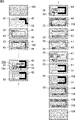
- FIG. 5 is an exploded view schematically showing a method for producing a laminated body by a printing laminating method.
- FIG. 5 shows the layer structure constituting the laminated body produced by the printing laminating method.
- the resin paste, the conductor paste, and the ceramic paste constituting each layer are printed in order based on the outer layer 100 which is the insulating layer shown at the bottom of FIG. Ceramic paste is a material that becomes an insulating layer by firing.
- Each layer shown in FIG. 5 shows the state of the upper surface after printing, and each layer shown in FIG. 5 is not separately manufactured and laminated.
- a ceramic paste, a conductor paste and a resin paste as materials are prepared.
- the ceramic paste it is preferable to use a magnetic ferrite paste and a non-magnetic ferrite paste.
- Fe is converted into Fe 2 O 3 and is 40 mol% or more and 49.5 mol% or less
- Zn is converted into ZnO and converted into 5 mol% or more and 35 mol% or less
- Cu is converted into CuO and is 4 mol%.
- the above magnetic ferrite material may contain trace additives (including unavoidable impurities) such as Mn, Co, Sn, Bi, and Si.
- trace additives including unavoidable impurities
- Fe is converted into Fe 2 O 3 and is 40 mol% or more and 49.5 mol% or less
- Cu is converted into Cu O and is 6 mol% or more and 12 mol% or less
- the balance is ZnO. It is preferable to use a material.
- the above non-magnetic ferrite material may contain trace additives (including unavoidable impurities) such as Mn, Co, Sn, Bi, and Si.
- Examples of the method for producing the ceramic paste include the following methods. Magnetic ferrite material or non-magnetic ferrite material and, if necessary, additives are weighed to a predetermined composition, placed in a ball mill, mixed and pulverized in a wet manner, discharged, evaporated and dried, and then 700. It is calcined at a temperature of ° C. or higher and 800 ° C. or lower to obtain a calcined powder. A predetermined amount of solvent (ketone solvent, etc.), resin (polyvinyl acetal, etc.), and plasticizer (alkyd plasticizer, etc.) are added to this calcined powder, kneaded with a planetary mixer, and then three roll mills are added. A ferrite paste is produced by dispersing in.
- a conductor paste is prepared by preparing silver powder, adding a predetermined amount of solvent (eugenol, etc.), resin (ethyl cellulose, etc.), and a dispersant, kneading with a planetary mixer, and dispersing with a three-roll mill.
- solvent eugenol, etc.
- resin ethyl cellulose, etc.
- dispersant kneading with a planetary mixer, and dispersing with a three-roll mill.
- the resin paste is a paste for forming a resin layer between a ceramic paste and a conductor paste, and a void is formed by burning the resin layer after firing.
- Examples of the method for producing the resin paste include the following methods.
- a resin paste is prepared by impregnating a solvent (dihydroterpinyl acetate, isophorone, etc.) with a resin (acrylic resin, etc.) that burns out during firing.
- a heat release sheet and a base film are stacked on a metal plate, and a magnetic ferrite paste is printed a predetermined number of times to prepare an outer layer.
- a PET (polyethylene terephthalate) film can be preferably used as the base film.
- the outer layer 100 is shown at the bottom of the right column of FIG.
- the resin paste is printed on the outer layer 100 to form the resin layer 150 so as to have the pattern shown second from the bottom in the right column of FIG. It is preferable that the pattern of the resin layer 150 is substantially the same as the pattern of the first coil conductor 31 to be formed later, and the line width of the resin layer 150 is slightly smaller than the conductor width of the first coil conductor 31.
- the conductor paste is printed on the portion to be the lead conductor 35 so as to have the pattern shown third from the bottom in the right column of FIG. Further, the conductor paste is printed so as to cover the resin layer 150 so as to have the pattern shown fourth from the bottom in the right column of FIG. 5, and the first coil conductor 31 is formed.
- the thickness of the lead conductor can be increased. By making the lead conductor thicker, the sealing performance of the laminated coil component can be improved.
- the magnetic ferrite paste is printed on the region where the lead conductor 35 and the first coil conductor 31 are not formed to form the insulating layer 41.
- the thickness of the insulating layer 41 is set to be substantially the same as the thickness of the lead conductor 35 and the first coil conductor 31, so that the surface composed of the insulating layer 41, the drawer conductor 35 and the first coil conductor 31 is a substantially flat surface.
- the fifth pattern from the bottom in the right column of FIG. 5 shows the upper surface after forming the insulating layer 41.
- the conductor paste to be the connecting conductor 33 is printed on the first coil conductor 31 so as to have the pattern shown sixth from the bottom in the right column of FIG.
- the connecting conductor 33 is formed so that the conductor width W3 of the connecting conductor 33 is smaller than the conductor width W1 of the first coil conductor 31.
- a non-magnetic ferrite paste is printed on the first coil conductor 31 to form the insulating layer 43 so as to have the pattern shown in the seventh from the bottom in the right column of FIG.
- the connecting conductor 33 is exposed on the upper surface.
- the insulating layer 43 is not formed on the lead conductor 35.
- a magnetic ferrite paste is printed around the insulating layer 43 to form the insulating layer 44.
- the surface composed of the insulating layer 43, the insulating layer 44, and the connecting conductor 33 is made to be a substantially flat surface.
- the eighth pattern from the bottom in the right column of FIG. 5 shows the upper surface after forming the insulating layer 44.
- the resin paste is printed to form the resin layer 150 so as to have the pattern shown in the ninth column from the bottom in the right column of FIG. It is preferable that the pattern of the resin layer 150 is substantially the same as the pattern of the second coil conductor 32 to be formed later, and the line width of the resin layer 150 is slightly smaller than the conductor width of the second coil conductor 32.
- the conductor width of the second coil conductor 32 referred to here means the conductor width other than the connecting portion connected to the connecting conductor 33. Further, the resin layer 150 is formed so as not to cover the upper surface of the connecting conductor 33 and its surroundings.
- the conductor paste is printed so as to cover the resin layer 150 so as to have the pattern shown tenth from the bottom in the right column of FIG. 5, and the second coil conductor 32 is formed.
- the connecting portion 34 is formed.
- the second coil conductor 32 is formed at the connection portion 34 so that the conductor width W2 of the second coil conductor 32 is smaller than the conductor width W1 of the first coil conductor 31.
- the conductor width W2 of the second coil conductor 32 may be the same as the conductor width W3 of the connecting conductor 33, and the conductor width W2 of the second coil conductor 32 may be smaller than the conductor width W3 of the connecting conductor 33.
- a magnetic ferrite paste is printed around the second coil conductor 32 to form the insulating layer 42 so as to have the pattern shown at the bottom of the left column of FIG.
- the insulating layer 42 is also formed in the portion of the connecting portion 34 where the insulating layer 43 is exposed.
- the surface composed of the insulating layer 42 and the second coil conductor 32 is made to be a substantially flat surface.
- the conductor paste to be the connecting conductor 33 is printed on the coil conductor described as the second coil conductor 32 so as to have the pattern shown second from the bottom in the left column of FIG.
- the position where the connecting conductor 33 is formed is a position advanced by one turn of the coil from the connecting portion 34 (connecting portion 34a) connected to the first coil conductor 31 in the lower layer.
- the conductor width W3 of the connecting conductor 33 is smaller than the conductor width W1 of the coil conductor previously described as the second coil conductor 32. That is, in this portion, the coil conductor previously described as the second coil conductor 32 becomes the first coil conductor 31.
- the coil conductor is the first coil conductor or the second coil conductor is determined by the relationship between the conductor width of the coil conductor and the conductor width of the other coil conductor connected at the connection portion. Therefore, the coil conductor shown in the second pattern from the bottom in the left column of FIG. 5 is the second coil conductor 32 at the left connection portion 34a connected to the lower layer coil conductor, and is connected to the upper layer coil conductor. It can be said that the connecting portion 34b on the right side is the first coil conductor 31.
- the formation of the insulating layer 43-the formation of the insulating layer 44-the formation of the resin layer 150-the formation of the second coil conductor 32-the formation of the insulating layer 42-the formation of the connecting conductor 33-... is repeated to form the laminated body.
- the conductor paste is printed on the portion to be the lead conductor 36 so as to have the pattern shown third from the bottom in the left column of FIG. Further, the conductor paste is printed so as to cover the resin layer 150 so as to have the pattern shown fourth from the bottom in the left column of FIG. 5, and the second coil conductor 32 is formed.
- a magnetic ferrite paste is printed in a region where the leader conductor 36 and the second coil conductor 32 are not formed to form the insulating layer 42 so as to have the pattern shown fifth from the bottom in the left column of FIG. ..
- the thickness of the insulating layer 42 is set to be substantially the same as the thickness of the lead conductor 36 and the second coil conductor 32, so that the surface composed of the insulating layer 42, the drawer conductor 36 and the second coil conductor 32 is a substantially flat surface.
- the ceramic paste is printed a predetermined number of times so as to cover the entire drawer conductor 36 and the second coil conductor 32 to form the outer layer 100.
- the metal plate and the base film are peeled off in this order after crimping while being attached to the metal plate, so that an aggregate having a large number of elements having the pattern shown above is provided on one surface (an aggregate (). Laminated block) is obtained.
- the laminated block is cut with a dicer or the like and individualized into elements.
- This element corresponds to one laminated coil component.
- the barrel treatment may be performed on an unfired element or may be performed on a laminated body after firing. Further, the barrel treatment may be either dry type or wet type.
- the barrel processing may be a method of rubbing the elements together or a method of barrel processing together with the media.
- the element is fired at a temperature of 910 ° C. or higher and 930 ° C. or lower to obtain a laminated body.
- the resin layer is burnt down and a gap is formed between the insulating layer and the coil conductor.
- a paste containing a metal is applied to the laminate and baked to form a base electrode. Subsequently, electrolytic plating is performed to form a Ni film and a Sn film on the base electrode in that order, whereby a first external electrode and a second external electrode can be formed, and a laminated coil component can be obtained.
- the pulverized material was dried and calcined at a temperature of 700 ° C. or higher and 800 ° C. or lower to obtain a calcined powder.
- a predetermined amount of solvent (ketone solvent, etc.), resin (polyvinyl acetal, etc.), and plasticizer (alkyd-based plasticizer, etc.) are added to this calcined powder, and the mixture is kneaded with a planetary mixer or the like, and then three more.
- a magnetic ferrite paste was prepared by dispersing with a roll mill.
- the pulverized material was dried and calcined at a temperature of 700 ° C. or higher and 800 ° C. or lower to obtain a calcined powder.
- a predetermined amount of solvent (ketone solvent, etc.), resin (polyvinyl acetal, etc.), and plasticizer (alkyd-based plasticizer, etc.) are added to this calcined powder, and the mixture is kneaded with a planetary mixer or the like, and then three more.
- a non-magnetic ferrite paste was prepared by dispersing with a roll mill.
- a conductor paste was prepared by preparing silver powder, adding a predetermined amount of solvent (eugenol, etc.), resin (ethyl cellulose, etc.), and a dispersant, kneading with a planetary mixer, and dispersing with a three-roll mill.
- solvent eugenol, etc.
- resin ethyl cellulose, etc.
- dispersant kneading with a planetary mixer, and dispersing with a three-roll mill.
- a resin paste was prepared by containing an acrylic resin in a solvent (dihydroterpinyl acetate).
- the conductor width W1 of the first coil conductor was 264 ⁇ m
- the conductor width W3 of the connecting conductor was 183 ⁇ m
- the conductor width W2 of the second coil conductor was 183 ⁇ m
- the crack occurrence rate was 0%.
- the conductor width W2 of the second coil conductor and the conductor width W3 of the connecting conductor are 69% of the conductor width W1 of the first coil conductor.
- the conductor width W1 of the first coil conductor was 180 ⁇ m
- the conductor width W2 of the second coil conductor was 145 ⁇ m
- the conductor width W3 of the connecting conductor was 145 ⁇ m.
- the crack occurrence rate was 0%.
- the conductor width W2 of the second coil conductor and the conductor width W3 of the connecting conductor are 81% of the conductor width W1 of the first coil conductor.
- the conductor width W1 of the first coil conductor was 350 ⁇ m
- the conductor width W2 of the second coil conductor was 210 ⁇ m
- the conductor width W3 of the connecting conductor was 210 ⁇ m.
- the crack occurrence rate was 0%.
- the conductor width W2 of the second coil conductor and the conductor width W3 of the connecting conductor are 60% of the conductor width W1 of the first coil conductor.
- the conductor width W1 of the first coil conductor was 256 ⁇ m
- the conductor width W2 of the second coil conductor was 188 ⁇ m
- the conductor width W3 of the connecting conductor was 212 ⁇ m. That is, the relationship of W1>W3> W2 is set. In this case, the crack occurrence rate was 0%.
- Table 1 summarizes the specifications and crack occurrence rate of the laminated body of the above 12 types of examples and 1 type of comparative example.
- Laminated coil component 10 Laminated body 11 First end surface 12 Second end surface 13 First main surface 14 Second main surface 15 First side surface 16 Second side surface 21 First external electrode 22 Second External electrode 30 Coil 31 1st coil conductor 32 2nd coil conductor 33 Connecting conductors 34, 34a, 34b, 34'Connecting parts 35, 36 Drawer conductor 41 Insulating layer 42 2nd coil located at the same height as the 1st coil conductor Insulation layer 43 located at the same height as the conductor Insulation layer 44 located between the first coil conductor and the second coil conductor Insulation layer around the insulation layer 43 100 Outer layer 150 Resin layer
Landscapes
- Engineering & Computer Science (AREA)
- Power Engineering (AREA)
- Microelectronics & Electronic Packaging (AREA)
- Coils Or Transformers For Communication (AREA)
Priority Applications (3)
| Application Number | Priority Date | Filing Date | Title |
|---|---|---|---|
| JP2022557428A JP7485073B2 (ja) | 2020-10-20 | 2021-10-14 | 積層型コイル部品 |
| CN202180071196.1A CN116529840A (zh) | 2020-10-20 | 2021-10-14 | 层叠型线圈部件 |
| US18/301,763 US20230253142A1 (en) | 2020-10-20 | 2023-04-17 | Multilayer coil component |
Applications Claiming Priority (2)
| Application Number | Priority Date | Filing Date | Title |
|---|---|---|---|
| JP2020176129 | 2020-10-20 | ||
| JP2020-176129 | 2020-10-20 |
Related Child Applications (1)
| Application Number | Title | Priority Date | Filing Date |
|---|---|---|---|
| US18/301,763 Continuation US20230253142A1 (en) | 2020-10-20 | 2023-04-17 | Multilayer coil component |
Publications (1)
| Publication Number | Publication Date |
|---|---|
| WO2022085552A1 true WO2022085552A1 (ja) | 2022-04-28 |
Family
ID=81290848
Family Applications (1)
| Application Number | Title | Priority Date | Filing Date |
|---|---|---|---|
| PCT/JP2021/038011 Ceased WO2022085552A1 (ja) | 2020-10-20 | 2021-10-14 | 積層型コイル部品 |
Country Status (4)
| Country | Link |
|---|---|
| US (1) | US20230253142A1 (https=) |
| JP (1) | JP7485073B2 (https=) |
| CN (1) | CN116529840A (https=) |
| WO (1) | WO2022085552A1 (https=) |
Citations (6)
| Publication number | Priority date | Publication date | Assignee | Title |
|---|---|---|---|---|
| JPH11297531A (ja) * | 1998-04-07 | 1999-10-29 | Taiyo Yuden Co Ltd | 積層電子部品 |
| JP2009044030A (ja) * | 2007-08-10 | 2009-02-26 | Hitachi Metals Ltd | 積層電子部品 |
| JP2011040612A (ja) * | 2009-08-12 | 2011-02-24 | Murata Mfg Co Ltd | 電子部品及びその製造方法 |
| JP2017028143A (ja) * | 2015-07-24 | 2017-02-02 | Tdk株式会社 | 積層コイル部品 |
| JP2019009211A (ja) * | 2017-06-22 | 2019-01-17 | 株式会社村田製作所 | 積層インダクタの製造方法および積層インダクタ |
| JP2019047015A (ja) * | 2017-09-05 | 2019-03-22 | 株式会社村田製作所 | コイル部品 |
Family Cites Families (9)
| Publication number | Priority date | Publication date | Assignee | Title |
|---|---|---|---|---|
| JP2001135548A (ja) | 1999-11-09 | 2001-05-18 | Tdk Corp | 電子部品およびその製造方法 |
| JP2002208515A (ja) * | 2001-01-09 | 2002-07-26 | Murata Mfg Co Ltd | 積層型インダクタ |
| JP2003092214A (ja) * | 2001-09-18 | 2003-03-28 | Murata Mfg Co Ltd | 積層型インダクタ |
| JP3942395B2 (ja) | 2001-10-01 | 2007-07-11 | コーア株式会社 | 積層チップ部品 |
| TWI280593B (en) * | 2005-06-16 | 2007-05-01 | Via Tech Inc | Inductor |
| JP4893773B2 (ja) * | 2009-04-02 | 2012-03-07 | 株式会社村田製作所 | 電子部品及びその製造方法 |
| JP5835355B2 (ja) | 2012-01-20 | 2015-12-24 | 株式会社村田製作所 | コイル部品 |
| JP5994933B2 (ja) * | 2013-05-08 | 2016-09-21 | 株式会社村田製作所 | 電子部品 |
| JP2015026760A (ja) * | 2013-07-29 | 2015-02-05 | 株式会社村田製作所 | 積層コイル |
-
2021
- 2021-10-14 WO PCT/JP2021/038011 patent/WO2022085552A1/ja not_active Ceased
- 2021-10-14 CN CN202180071196.1A patent/CN116529840A/zh active Pending
- 2021-10-14 JP JP2022557428A patent/JP7485073B2/ja active Active
-
2023
- 2023-04-17 US US18/301,763 patent/US20230253142A1/en active Pending
Patent Citations (6)
| Publication number | Priority date | Publication date | Assignee | Title |
|---|---|---|---|---|
| JPH11297531A (ja) * | 1998-04-07 | 1999-10-29 | Taiyo Yuden Co Ltd | 積層電子部品 |
| JP2009044030A (ja) * | 2007-08-10 | 2009-02-26 | Hitachi Metals Ltd | 積層電子部品 |
| JP2011040612A (ja) * | 2009-08-12 | 2011-02-24 | Murata Mfg Co Ltd | 電子部品及びその製造方法 |
| JP2017028143A (ja) * | 2015-07-24 | 2017-02-02 | Tdk株式会社 | 積層コイル部品 |
| JP2019009211A (ja) * | 2017-06-22 | 2019-01-17 | 株式会社村田製作所 | 積層インダクタの製造方法および積層インダクタ |
| JP2019047015A (ja) * | 2017-09-05 | 2019-03-22 | 株式会社村田製作所 | コイル部品 |
Also Published As
| Publication number | Publication date |
|---|---|
| JP7485073B2 (ja) | 2024-05-16 |
| US20230253142A1 (en) | 2023-08-10 |
| CN116529840A (zh) | 2023-08-01 |
| JPWO2022085552A1 (https=) | 2022-04-28 |
Similar Documents
| Publication | Publication Date | Title |
|---|---|---|
| JP2020035788A (ja) | 電子部品 | |
| JP5610081B2 (ja) | 電子部品及びその製造方法 | |
| JP7099345B2 (ja) | コイル部品 | |
| JP2020053577A (ja) | 電子部品 | |
| CN113053620B (zh) | 层叠线圈部件 | |
| CN113380510A (zh) | 层叠线圈部件 | |
| JP6303368B2 (ja) | 電子部品及びその製造方法 | |
| JP2021125596A (ja) | 積層コイル部品 | |
| JP7548379B2 (ja) | 積層型コイル部品 | |
| WO2021106477A1 (ja) | 積層型コイル部品 | |
| JP2021108326A (ja) | 積層コイル部品 | |
| JP2021125597A (ja) | コイル部品 | |
| JP2018056513A (ja) | 電子部品 | |
| JP4461814B2 (ja) | 積層セラミック電子部品の製造方法 | |
| JP4400430B2 (ja) | 積層型インダクタ | |
| WO2022085552A1 (ja) | 積層型コイル部品 | |
| JP2021108325A (ja) | 積層コイル部品 | |
| US12573544B2 (en) | Multilayer coil component | |
| CN218957480U (zh) | 层叠线圈部件 | |
| JP7456771B2 (ja) | 積層コイル部品 | |
| JP7605171B2 (ja) | 電子部品 | |
| US11769617B2 (en) | Laminated coil component | |
| JP2021136345A (ja) | コイル部品 | |
| JP7694695B2 (ja) | 積層コイル部品 | |
| US20240304367A1 (en) | Multilayer coil component |
Legal Events
| Date | Code | Title | Description |
|---|---|---|---|
| 121 | Ep: the epo has been informed by wipo that ep was designated in this application |
Ref document number: 21882693 Country of ref document: EP Kind code of ref document: A1 |
|
| ENP | Entry into the national phase |
Ref document number: 2022557428 Country of ref document: JP Kind code of ref document: A |
|
| WWE | Wipo information: entry into national phase |
Ref document number: 202180071196.1 Country of ref document: CN |
|
| NENP | Non-entry into the national phase |
Ref country code: DE |
|
| 122 | Ep: pct application non-entry in european phase |
Ref document number: 21882693 Country of ref document: EP Kind code of ref document: A1 |