WO2022085552A1 - Stacked coil component - Google Patents
Stacked coil component Download PDFInfo
- Publication number
- WO2022085552A1 WO2022085552A1 PCT/JP2021/038011 JP2021038011W WO2022085552A1 WO 2022085552 A1 WO2022085552 A1 WO 2022085552A1 JP 2021038011 W JP2021038011 W JP 2021038011W WO 2022085552 A1 WO2022085552 A1 WO 2022085552A1
- Authority
- WO
- WIPO (PCT)
- Prior art keywords
- conductor
- coil
- width
- coil conductor
- laminated
- Prior art date
Links
- 239000004020 conductor Substances 0.000 claims abstract description 520
- 239000000696 magnetic material Substances 0.000 claims description 11
- 229910000859 α-Fe Inorganic materials 0.000 description 31
- 239000011347 resin Substances 0.000 description 30
- 229920005989 resin Polymers 0.000 description 30
- 238000000034 method Methods 0.000 description 22
- 239000000463 material Substances 0.000 description 18
- 238000004519 manufacturing process Methods 0.000 description 11
- 239000002904 solvent Substances 0.000 description 10
- 238000010030 laminating Methods 0.000 description 9
- BQCADISMDOOEFD-UHFFFAOYSA-N Silver Chemical compound [Ag] BQCADISMDOOEFD-UHFFFAOYSA-N 0.000 description 8
- 239000000919 ceramic Substances 0.000 description 8
- 239000000654 additive Substances 0.000 description 7
- 239000002184 metal Substances 0.000 description 7
- 229910052751 metal Inorganic materials 0.000 description 7
- 230000035882 stress Effects 0.000 description 7
- 230000015572 biosynthetic process Effects 0.000 description 6
- 238000010304 firing Methods 0.000 description 6
- 239000004014 plasticizer Substances 0.000 description 6
- 239000000843 powder Substances 0.000 description 6
- 229910052709 silver Inorganic materials 0.000 description 6
- 239000004332 silver Substances 0.000 description 6
- 239000010949 copper Substances 0.000 description 5
- 239000011810 insulating material Substances 0.000 description 5
- 239000000203 mixture Substances 0.000 description 5
- 229910052797 bismuth Inorganic materials 0.000 description 4
- -1 etc.) Substances 0.000 description 4
- RRAFCDWBNXTKKO-UHFFFAOYSA-N eugenol Chemical compound COC1=CC(CC=C)=CC=C1O RRAFCDWBNXTKKO-UHFFFAOYSA-N 0.000 description 4
- 239000012535 impurity Substances 0.000 description 4
- 238000009413 insulation Methods 0.000 description 4
- 229910052748 manganese Inorganic materials 0.000 description 4
- 238000002360 preparation method Methods 0.000 description 4
- 229910052710 silicon Inorganic materials 0.000 description 4
- 229910052718 tin Inorganic materials 0.000 description 4
- DHKHKXVYLBGOIT-UHFFFAOYSA-N acetaldehyde Diethyl Acetal Natural products CCOC(C)OCC DHKHKXVYLBGOIT-UHFFFAOYSA-N 0.000 description 3
- 150000001241 acetals Chemical class 0.000 description 3
- 229920000180 alkyd Polymers 0.000 description 3
- 150000002576 ketones Chemical class 0.000 description 3
- 229920002554 vinyl polymer Polymers 0.000 description 3
- HBNHCGDYYBMKJN-UHFFFAOYSA-N 2-(4-methylcyclohexyl)propan-2-yl acetate Chemical compound CC1CCC(C(C)(C)OC(C)=O)CC1 HBNHCGDYYBMKJN-UHFFFAOYSA-N 0.000 description 2
- 239000004925 Acrylic resin Substances 0.000 description 2
- 229920000178 Acrylic resin Polymers 0.000 description 2
- NPBVQXIMTZKSBA-UHFFFAOYSA-N Chavibetol Natural products COC1=CC=C(CC=C)C=C1O NPBVQXIMTZKSBA-UHFFFAOYSA-N 0.000 description 2
- 239000001856 Ethyl cellulose Substances 0.000 description 2
- ZZSNKZQZMQGXPY-UHFFFAOYSA-N Ethyl cellulose Chemical compound CCOCC1OC(OC)C(OCC)C(OCC)C1OC1C(O)C(O)C(OC)C(CO)O1 ZZSNKZQZMQGXPY-UHFFFAOYSA-N 0.000 description 2
- 239000005770 Eugenol Substances 0.000 description 2
- UVMRYBDEERADNV-UHFFFAOYSA-N Pseudoeugenol Natural products COC1=CC(C(C)=C)=CC=C1O UVMRYBDEERADNV-UHFFFAOYSA-N 0.000 description 2
- 230000000996 additive effect Effects 0.000 description 2
- 229910052802 copper Inorganic materials 0.000 description 2
- 239000002270 dispersing agent Substances 0.000 description 2
- 238000006073 displacement reaction Methods 0.000 description 2
- 229920001249 ethyl cellulose Polymers 0.000 description 2
- 235000019325 ethyl cellulose Nutrition 0.000 description 2
- 229960002217 eugenol Drugs 0.000 description 2
- 238000000605 extraction Methods 0.000 description 2
- 238000010438 heat treatment Methods 0.000 description 2
- HJOVHMDZYOCNQW-UHFFFAOYSA-N isophorone Chemical compound CC1=CC(=O)CC(C)(C)C1 HJOVHMDZYOCNQW-UHFFFAOYSA-N 0.000 description 2
- 238000004898 kneading Methods 0.000 description 2
- 239000007769 metal material Substances 0.000 description 2
- 229920000139 polyethylene terephthalate Polymers 0.000 description 2
- 239000005020 polyethylene terephthalate Substances 0.000 description 2
- 229910052725 zinc Inorganic materials 0.000 description 2
- RYGMFSIKBFXOCR-UHFFFAOYSA-N Copper Chemical compound [Cu] RYGMFSIKBFXOCR-UHFFFAOYSA-N 0.000 description 1
- 230000000052 comparative effect Effects 0.000 description 1
- 239000012141 concentrate Substances 0.000 description 1
- 238000002788 crimping Methods 0.000 description 1
- 238000005553 drilling Methods 0.000 description 1
- 230000000694 effects Effects 0.000 description 1
- 238000009713 electroplating Methods 0.000 description 1
- 238000003475 lamination Methods 0.000 description 1
- 238000007789 sealing Methods 0.000 description 1
- 230000008646 thermal stress Effects 0.000 description 1
- 239000011800 void material Substances 0.000 description 1
Images


Classifications
-
- H—ELECTRICITY
- H01—ELECTRIC ELEMENTS
- H01F—MAGNETS; INDUCTANCES; TRANSFORMERS; SELECTION OF MATERIALS FOR THEIR MAGNETIC PROPERTIES
- H01F27/00—Details of transformers or inductances, in general
- H01F27/28—Coils; Windings; Conductive connections
- H01F27/2804—Printed windings
-
- H—ELECTRICITY
- H01—ELECTRIC ELEMENTS
- H01F—MAGNETS; INDUCTANCES; TRANSFORMERS; SELECTION OF MATERIALS FOR THEIR MAGNETIC PROPERTIES
- H01F17/00—Fixed inductances of the signal type
- H01F17/0006—Printed inductances
- H01F17/0013—Printed inductances with stacked layers
-
- H—ELECTRICITY
- H01—ELECTRIC ELEMENTS
- H01F—MAGNETS; INDUCTANCES; TRANSFORMERS; SELECTION OF MATERIALS FOR THEIR MAGNETIC PROPERTIES
- H01F27/00—Details of transformers or inductances, in general
- H01F27/28—Coils; Windings; Conductive connections
- H01F27/29—Terminals; Tapping arrangements for signal inductances
- H01F27/292—Surface mounted devices
-
- H—ELECTRICITY
- H01—ELECTRIC ELEMENTS
- H01F—MAGNETS; INDUCTANCES; TRANSFORMERS; SELECTION OF MATERIALS FOR THEIR MAGNETIC PROPERTIES
- H01F27/00—Details of transformers or inductances, in general
- H01F27/28—Coils; Windings; Conductive connections
- H01F27/32—Insulating of coils, windings, or parts thereof
- H01F27/323—Insulation between winding turns, between winding layers
-
- H—ELECTRICITY
- H01—ELECTRIC ELEMENTS
- H01F—MAGNETS; INDUCTANCES; TRANSFORMERS; SELECTION OF MATERIALS FOR THEIR MAGNETIC PROPERTIES
- H01F17/00—Fixed inductances of the signal type
- H01F17/0006—Printed inductances
- H01F17/0013—Printed inductances with stacked layers
- H01F2017/002—Details of via holes for interconnecting the layers
-
- H—ELECTRICITY
- H01—ELECTRIC ELEMENTS
- H01F—MAGNETS; INDUCTANCES; TRANSFORMERS; SELECTION OF MATERIALS FOR THEIR MAGNETIC PROPERTIES
- H01F17/00—Fixed inductances of the signal type
- H01F17/04—Fixed inductances of the signal type with magnetic core
- H01F2017/048—Fixed inductances of the signal type with magnetic core with encapsulating core, e.g. made of resin and magnetic powder
-
- H—ELECTRICITY
- H01—ELECTRIC ELEMENTS
- H01F—MAGNETS; INDUCTANCES; TRANSFORMERS; SELECTION OF MATERIALS FOR THEIR MAGNETIC PROPERTIES
- H01F27/00—Details of transformers or inductances, in general
- H01F27/28—Coils; Windings; Conductive connections
- H01F27/2804—Printed windings
- H01F2027/2809—Printed windings on stacked layers
-
- H—ELECTRICITY
- H01—ELECTRIC ELEMENTS
- H01F—MAGNETS; INDUCTANCES; TRANSFORMERS; SELECTION OF MATERIALS FOR THEIR MAGNETIC PROPERTIES
- H01F41/00—Apparatus or processes specially adapted for manufacturing or assembling magnets, inductances or transformers; Apparatus or processes specially adapted for manufacturing materials characterised by their magnetic properties
- H01F41/02—Apparatus or processes specially adapted for manufacturing or assembling magnets, inductances or transformers; Apparatus or processes specially adapted for manufacturing materials characterised by their magnetic properties for manufacturing cores, coils, or magnets
- H01F41/04—Apparatus or processes specially adapted for manufacturing or assembling magnets, inductances or transformers; Apparatus or processes specially adapted for manufacturing materials characterised by their magnetic properties for manufacturing cores, coils, or magnets for manufacturing coils
- H01F41/041—Printed circuit coils
-
- H—ELECTRICITY
- H01—ELECTRIC ELEMENTS
- H01F—MAGNETS; INDUCTANCES; TRANSFORMERS; SELECTION OF MATERIALS FOR THEIR MAGNETIC PROPERTIES
- H01F41/00—Apparatus or processes specially adapted for manufacturing or assembling magnets, inductances or transformers; Apparatus or processes specially adapted for manufacturing materials characterised by their magnetic properties
- H01F41/02—Apparatus or processes specially adapted for manufacturing or assembling magnets, inductances or transformers; Apparatus or processes specially adapted for manufacturing materials characterised by their magnetic properties for manufacturing cores, coils, or magnets
- H01F41/04—Apparatus or processes specially adapted for manufacturing or assembling magnets, inductances or transformers; Apparatus or processes specially adapted for manufacturing materials characterised by their magnetic properties for manufacturing cores, coils, or magnets for manufacturing coils
- H01F41/12—Insulating of windings
- H01F41/122—Insulating between turns or between winding layers
-
- H—ELECTRICITY
- H03—ELECTRONIC CIRCUITRY
- H03H—IMPEDANCE NETWORKS, e.g. RESONANT CIRCUITS; RESONATORS
- H03H7/00—Multiple-port networks comprising only passive electrical elements as network components
Definitions
- the present invention relates to a laminated coil component.
- Patent Document 1 discloses a laminated coil component containing a coil inside an insulating prime field having a laminated structure, in which adjacent coil portions are connected by a layered connecting portion.
- the connecting portion is arranged at a position corresponding to the position of the divided portion of the coil portion, and has a rectangular shape extending along the shape of the divided portion. Further, Patent Document 1 shows a structure in which the thicknesses of the upper coil layer and the lower coil layer of the connecting portion in the stacking direction are different. Patent Document 1 states that it is possible to provide a laminated coil component in which the number of types of coil portions constituting the coil is reduced.
- connection part of the laminated coil component is made of a conductor containing a metal such as silver, and an insulating layer made of an insulating material such as ferrite exists around the connection part.
- thermal stress generated by the difference in linear expansion coefficient between the conductor and the insulating material at the connection portion during the heat treatment in the process of processing the laminated coil component, especially in the temperature lowering process in which the temperature changes from high temperature to low temperature. Concentrate. Specifically, tensile stress is generated in the insulating layer when the conductor contracts. If the tensile stress is larger than the strength of the insulating layer, cracks may occur in the insulating layer around the connection portion.
- the present invention has been made to solve the above problems, and an object of the present invention is to provide a laminated coil component in which cracks are unlikely to occur around a connecting conductor connecting the coil conductors.
- the laminated coil component of the present invention has a laminated body in which a plurality of insulating layers are laminated and has a built-in coil, and an external surface provided on the outer surface of the laminated body and electrically connected to the coil.
- the conductor width of the connecting conductor is smaller than the conductor width of the first coil conductor, and the second coil conductor is described.
- the conductor width of the coil conductor is smaller than the conductor width of the first coil conductor.
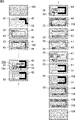
- FIG. 1 is a perspective view schematically showing an example of a laminated coil component of the present invention.
- FIG. 2 is a schematic view schematically showing the laminated coil component of the present invention through the inside so that the structure of the coil can be understood.
- FIG. 3 is a sectional view taken along line AA of FIG. 2, schematically showing the details of the connection portion.
- FIG. 4 is a cross-sectional view schematically showing another example of the connecting portion.
- FIG. 5 is an exploded view schematically showing a method for producing a laminated body by a printing laminating method.
- the laminated coil component of the present invention will be described.
- the present invention is not limited to the following configurations and embodiments, and can be appropriately modified and applied without changing the gist of the present invention. It should be noted that a combination of two or more of the individual preferred configurations and embodiments of the present invention described below is also the present invention.
- FIG. 1 is a perspective view schematically showing an example of a laminated coil component of the present invention.
- FIG. 2 is a schematic view schematically showing the laminated coil component of the present invention through the inside so that the structure of the coil can be understood.
- the laminated coil component 1 shown in FIG. 1 includes a laminated body 10, a first external electrode 21, and a second external electrode 22.
- the laminated body 10 has a substantially rectangular parallelepiped shape having six faces. Although the configuration of the laminated body 10 will be described later, a plurality of insulating layers are laminated and a coil is built in the laminated body 10.
- the first external electrode 21 and the second external electrode 22 are each electrically connected to the coil.
- the direction in which the first external electrode and the second external electrode face each other is defined as the length direction.
- the direction orthogonal to the length direction is defined as the height direction
- the direction orthogonal to the length direction and the height direction is defined as the width direction.
- 1 and 2 show the length direction, the width direction, and the height direction of the laminated coil component and the laminated body as the double-headed arrow L direction, W direction, and T direction, respectively.
- the length direction (L direction), the width direction (W direction), and the height direction (T direction) are orthogonal to each other.
- the mounting surface of the laminated coil component 1 is a surface (LW surface) parallel to the length direction and the width direction.
- the laminate 10 shown in FIGS. 1 and 2 has a first end surface 11 and a second end surface 12 facing in the length direction, and a first main surface 13 and a first main surface 13 facing in the height direction orthogonal to the length direction. It has a second main surface 14 and a first side surface 15 and a second side surface 16 facing each other in the width direction orthogonal to the length direction and the height direction.
- the laminated body 10 has rounded corners and ridges.
- the corner portion is a portion where the three surfaces of the laminated body intersect, and the ridge portion is a portion where the two surfaces of the laminated body intersect.
- the first external electrode 21 covers the first end surface 11 of the laminated body 10 and extends from the first end surface 11 to be a part of the first main surface 13 and the second main surface. It is arranged so as to cover a part of the surface 14, a part of the first side surface 15, and a part of the second side surface 16.
- the second external electrode 22 covers the second end surface 12 of the laminated body 10, extends from the second end surface 12, and is a part of the first main surface 13, the second. It is arranged so as to cover a part of the main surface 14, a part of the first side surface 15, and a part of the second side surface 16.
- the second main surface 14 is the mounting surface.
- the coil is formed by electrically connecting a plurality of coil conductors laminated together with an insulating layer.
- the stacking direction of the laminated body which is the direction in which the plurality of insulating layers are laminated, is along the height direction. Further, the coil axis of the coil is along the height direction.
- the coil conductor and the first external electrode are electrically connected at the first end face, and the coil conductor and the second external electrode are electrically connected at the second end face.
- the coil conductor constituting the coil 30 and the first external electrode 21 are electrically connected by the first end surface 11, and the coil conductor and the second external electrode 22 are electrically connected by the second end surface 12. It shows how it is connected to.
- the conductor that draws the coil 30 to the first end surface 11 is the extraction conductor 35
- the conductor that draws the coil 30 to the second end surface 12 is the extraction conductor 36.
- the connection position between the coil conductor and the external electrode can be changed by changing the position where the coil conductor is pulled out to the outside of the laminate. The drawing position may be changed so that the coil conductor and the external electrode are electrically connected on the main surface or the side surface of the laminated body.
- FIG. 2 shows that adjacent coil conductors are connected via a connecting conductor.
- the adjacent coil conductor connected via the connecting conductor 33 is the first coil conductor 31 or the second coil conductor 32.
- the portion where the first coil conductor 31 and the second coil conductor 32, which are adjacent coil conductors, are connected via the connecting conductor 33 is referred to as a connecting portion 34. That is, the connecting portion is a portion where the first coil conductor comes into contact with the connecting conductor, a portion where the second coil conductor comes into contact with the connecting conductor, and a portion composed of the connecting conductor.
- the conductor width of the connecting conductor 33 is smaller than the conductor width of the first coil conductor 31, and the conductor width of the second coil conductor 32 is the conductor of the first coil conductor 31. Smaller than the width.
- the coil conductor located on the lower side in the height direction is the first coil conductor 31, and the coil located on the upper side in the height direction.
- the conductor is the second coil conductor 32.
- the coil conductor located on the lower side in the height direction is the first coil conductor 31, and the coil conductor located on the upper side in the height direction is the second coil conductor 32. ..
- one coil conductor connected via the connecting conductor 33 becomes the first coil conductor 31, and the other coil conductor becomes the second coil conductor 32. Comparing the conductor width of the connecting conductor, the conductor width of one coil conductor, and the conductor width of the other coil conductor, the coil conductor with the larger conductor width is the first coil conductor, and the coil conductor with the smaller conductor width. Is the second coil conductor. Then, the conductor width of the first coil conductor becomes larger than the conductor width of the connecting conductor. In the connection portion 34 shown in FIG. 2, the first coil conductor 31 is located below and the second coil conductor 32 is located above, but whether it is the first coil conductor or the second coil conductor depends on the conductor width. It is determined, not up and down with respect to the height direction (stacking direction).
- FIG. 3 is a sectional view taken along line AA of FIG. 2, schematically showing the details of the connection portion.
- FIG. 3 shows the first coil conductor 31, the second coil conductor 32, and the connecting conductor 33 constituting the connecting portion 34.
- the conductor width of the first coil conductor 31 is the width indicated by the double-headed arrow W1
- the conductor width of the second coil conductor 32 is the width indicated by the double-headed arrow W2
- the conductor width of the connecting conductor 33 is the width indicated by the double-headed arrow W3.
- the width of each conductor is defined as the width at which the conductor width is the widest.
- the conductor width of the connecting conductor 33 is smaller than the conductor width of the first coil conductor 31, and the conductor width of the second coil conductor 32 is smaller than the conductor width of the first coil conductor 31.
- W3 ⁇ W1 and W2 ⁇ W1 in FIG. 3 the conductor width W3 of the connecting conductor 33 and the conductor width W2 of the second coil conductor 32 are the same, but the conductor width W3 of the connecting conductor 33 and the conductor width W2 of the second coil conductor 32 are the same. It may be different.
- the heat treatment when processing the laminated coil component causes stress in the insulating layer made of an insulating material such as ferrite. This is because the coefficient of linear expansion of a metal such as silver constituting the conductor portion and an insulating material such as ferrite are different.
- a metal such as silver constituting the conductor portion and an insulating material such as ferrite are different.
- tensile stress is generated in the insulating layer when the conductor contracts.
- the larger the displacement of the conductor the larger the tensile stress.
- the tensile stress becomes larger than the strength of the insulating layer, cracks occur in the insulating layer.
- the conductor width of one coil conductor (second coil conductor) smaller than the conductor width of the other coil conductor (first coil conductor)
- the amount of displacement of the conductor is small. Since the tensile stress generated in the insulating layer is reduced, the occurrence of cracks can be prevented.
- the conductor width of the first coil conductor is preferably 180 ⁇ m or more and 380 ⁇ m or less. Further, the conductor width of the first coil conductor other than the connecting portion is preferably the same as the conductor width in the connecting portion, and is preferably 180 ⁇ m or more and 380 ⁇ m or less.
- the conductor width of the second coil conductor is smaller than the conductor width of the first coil conductor, and the conductor width of the second coil conductor is 30% or more and 90% or less of the conductor width of the first coil conductor. Is preferable.
- the conductor width of the second coil conductor is set to 90 of the conductor width of the first coil conductor in consideration of the manufacturing tolerance and the like. It is preferable to set it to% or less.
- the conductor width of the second coil conductor is smaller than 30% of the conductor width of the first coil conductor, the conductor width of the second coil conductor may become too small and the second coil conductor may be disconnected. Further, it is preferable that the difference between the conductor width of the second coil conductor and the conductor width of the first coil conductor is 40 ⁇ m or more and 200 ⁇ m or less. From these viewpoints, the conductor width of the second coil conductor is preferably 55 ⁇ m or more and 340 ⁇ m or less.
- the conductor width of the second coil conductor other than the connecting portion is preferably larger than the conductor width of the second coil conductor at the connecting portion, and is preferably 180 ⁇ m or more and 380 ⁇ m or less. Except for the connection portion, the conductor width of the first coil conductor and the conductor width of the second coil conductor may be the same, and the conductor width of the second coil conductor may be larger than the conductor width of the first coil conductor.
- the conductor thickness of the first coil conductor is preferably 20 ⁇ m or more at the connecting portion. Further, the conductor thickness of the second coil conductor is preferably 20 ⁇ m or more at the connecting portion.
- the conductor thickness of the coil conductor is 20 ⁇ m or more and is thick, cracks tend to occur at the connection portion.
- the width of the coil conductor and the connection conductor at the connection portion has a predetermined relationship. Therefore, it is possible to prevent cracks from occurring at the connection portion even if the coil conductor is thick.
- the conductor width of the connecting conductor is smaller than the conductor width of the first coil conductor, and the conductor width of the connecting conductor is preferably 30% or more and 90% or less of the conductor width of the first coil conductor.
- the conductor width of the connecting conductor is set to 90% or less of the conductor width of the first coil conductor in consideration of the manufacturing tolerance and the like. It is preferable to do so. Further, if the conductor width of the connecting conductor is smaller than 30% of the conductor width of the first coil conductor, the conductor width of the connecting conductor may become too small and the connecting conductor may be broken.
- the difference between the conductor width of the connecting conductor and the conductor width of the first coil conductor is 40 ⁇ m or more and 200 ⁇ m or less.
- the conductor width of the connecting conductor is preferably 55 ⁇ m or more and 340 ⁇ m or less.
- the protruding width of the first coil conductor 31 projecting with respect to the second coil conductor 32 and the connecting conductor 33 is indicated by the double-headed arrow w.
- the first coil conductor 31 protrudes from both the left and right sides of the second coil conductor 32 and the connecting conductor 33.
- the preferable relationship between the width of the first coil conductor and the protrusion width w is, for example, as follows.
- the width of the first coil conductor is 200 ⁇ m or more and less than 300 ⁇ m
- the protrusion width is 20 ⁇ m or more and 80 ⁇ m or less.
- the protrusion width is 40 ⁇ m or more and 100 ⁇ m or less.
- the first coil conductor, the second coil conductor, and the connecting conductor preferably contain a metal, preferably copper, silver, and the like, and more preferably silver.
- a magnetic material or a non-magnetic material can be used as the material of the insulating layer.
- a magnetic ferrite material can be used as the magnetic material. Fe is converted to Fe 2 O 3 and is 40 mol% or more and 49.5 mol% or less, Zn is converted to ZnO and is 5 mol% or more and 35 mol% or less, and Cu is converted to CuO and is 4 mol% or more and 12 mol% or less.
- a magnetic ferrite material having a balance of NiO can be preferably used.
- the above magnetic ferrite material may contain trace additives (including unavoidable impurities) such as Mn, Co, Sn, Bi, and Si.
- a non-magnetic ferrite material As the non-magnetic material, a non-magnetic ferrite material can be used. It is preferable to use a non-magnetic ferrite material in which Fe is 40 mol% or more and 49.5 mol% or less in terms of Fe 2 O 3 , and Cu is 4 mol% or more and 12 mol% or less in terms of CuO, and the balance is ZnO. can.
- the above non-magnetic ferrite material may contain trace additives (including unavoidable impurities) such as Mn, Co, Sn, Bi, and Si.
- the insulating layer includes an insulating layer located at the same height as the first coil conductor, an insulating layer located at the same height as the second coil conductor, and an insulating layer located at the same height as the connecting conductor.
- the insulating layer located at the same height as the connecting conductor includes an insulating layer located between the first coil conductor and the second coil conductor, and an insulating layer located between the first coil conductor and the second coil conductor. There is an insulating layer around.
- the insulating layer located between the first coil conductor and the second coil conductor is preferably made of a non-magnetic material. When the insulating layer located between the first coil conductor and the second coil conductor is made of a non-magnetic material, magnetic saturation is less likely to occur, and the DC superimposition characteristic of the laminated coil component can be improved.
- the insulating layer located at the same height as the first coil conductor and the insulating layer located at the same height as the second coil conductor are preferably made of a magnetic material.
- FIG. 3 shows an insulating layer 41 located at the same height as the first coil conductor and an insulating layer 42 located at the same height as the second coil conductor.
- the insulating layer 41 and the insulating layer 42 are preferably an insulating layer made of a magnetic material.
- FIG. 3 also shows an insulating layer 43 located between the first coil conductor and the second coil conductor.
- the insulating layer 43 is preferably an insulating layer made of a non-magnetic material.
- the insulating layer around the insulating layer located between the first coil conductor and the second coil conductor is preferably made of a magnetic material.
- This insulating layer is an insulating layer represented by reference numeral 44 in FIG. 5, which will be described later.
- the laminated coil component of the present invention has a connection portion when the difference between the linear expansion coefficient of the metal material constituting the coil conductor or the connecting conductor and the linear expansion coefficient of the insulating material such as ferrite constituting the insulating layer is large. It is possible to prevent cracks from occurring in the surrounding insulating layer.
- the metal material constituting the coil conductor or the connecting conductor is silver and the material constituting the insulating layer is ferrite
- the difference in coefficient of linear expansion is preferably 11 ppm / K or more and 29 ppm / K or less.
- FIG. 4 is a cross-sectional view schematically showing another example of the connecting portion.
- the conductor width of the connecting conductor 33 is smaller than the conductor width of the first coil conductor 31 and the conductor width of the second coil conductor 32 is similar to that of the connection portion 34 shown in FIG. However, it is smaller than the conductor width of the first coil conductor 31.
- the conductor width W2 of the second coil conductor 32 is smaller than the conductor width W3 of the connecting conductor 33. That is, W2 ⁇ W3.
- the structure can be made so that cracks are least likely to occur.
- the print laminating method is a method of forming a coil conductor extending in the laminating direction of a laminated body by printing and laminating a conductor paste and a ceramic paste. This method is different from the method of producing a sheet having a via conductor in the sheet by drilling a laser hole in the sheet and filling the hole with a conductor paste, and laminating a plurality of the sheets.
- FIG. 5 is an exploded view schematically showing a method for producing a laminated body by a printing laminating method.
- FIG. 5 shows the layer structure constituting the laminated body produced by the printing laminating method.
- the resin paste, the conductor paste, and the ceramic paste constituting each layer are printed in order based on the outer layer 100 which is the insulating layer shown at the bottom of FIG. Ceramic paste is a material that becomes an insulating layer by firing.
- Each layer shown in FIG. 5 shows the state of the upper surface after printing, and each layer shown in FIG. 5 is not separately manufactured and laminated.
- a ceramic paste, a conductor paste and a resin paste as materials are prepared.
- the ceramic paste it is preferable to use a magnetic ferrite paste and a non-magnetic ferrite paste.
- Fe is converted into Fe 2 O 3 and is 40 mol% or more and 49.5 mol% or less
- Zn is converted into ZnO and converted into 5 mol% or more and 35 mol% or less
- Cu is converted into CuO and is 4 mol%.
- the above magnetic ferrite material may contain trace additives (including unavoidable impurities) such as Mn, Co, Sn, Bi, and Si.
- trace additives including unavoidable impurities
- Fe is converted into Fe 2 O 3 and is 40 mol% or more and 49.5 mol% or less
- Cu is converted into Cu O and is 6 mol% or more and 12 mol% or less
- the balance is ZnO. It is preferable to use a material.
- the above non-magnetic ferrite material may contain trace additives (including unavoidable impurities) such as Mn, Co, Sn, Bi, and Si.
- Examples of the method for producing the ceramic paste include the following methods. Magnetic ferrite material or non-magnetic ferrite material and, if necessary, additives are weighed to a predetermined composition, placed in a ball mill, mixed and pulverized in a wet manner, discharged, evaporated and dried, and then 700. It is calcined at a temperature of ° C. or higher and 800 ° C. or lower to obtain a calcined powder. A predetermined amount of solvent (ketone solvent, etc.), resin (polyvinyl acetal, etc.), and plasticizer (alkyd plasticizer, etc.) are added to this calcined powder, kneaded with a planetary mixer, and then three roll mills are added. A ferrite paste is produced by dispersing in.
- a conductor paste is prepared by preparing silver powder, adding a predetermined amount of solvent (eugenol, etc.), resin (ethyl cellulose, etc.), and a dispersant, kneading with a planetary mixer, and dispersing with a three-roll mill.
- solvent eugenol, etc.
- resin ethyl cellulose, etc.
- dispersant kneading with a planetary mixer, and dispersing with a three-roll mill.
- the resin paste is a paste for forming a resin layer between a ceramic paste and a conductor paste, and a void is formed by burning the resin layer after firing.
- Examples of the method for producing the resin paste include the following methods.
- a resin paste is prepared by impregnating a solvent (dihydroterpinyl acetate, isophorone, etc.) with a resin (acrylic resin, etc.) that burns out during firing.
- a heat release sheet and a base film are stacked on a metal plate, and a magnetic ferrite paste is printed a predetermined number of times to prepare an outer layer.
- a PET (polyethylene terephthalate) film can be preferably used as the base film.
- the outer layer 100 is shown at the bottom of the right column of FIG.
- the resin paste is printed on the outer layer 100 to form the resin layer 150 so as to have the pattern shown second from the bottom in the right column of FIG. It is preferable that the pattern of the resin layer 150 is substantially the same as the pattern of the first coil conductor 31 to be formed later, and the line width of the resin layer 150 is slightly smaller than the conductor width of the first coil conductor 31.
- the conductor paste is printed on the portion to be the lead conductor 35 so as to have the pattern shown third from the bottom in the right column of FIG. Further, the conductor paste is printed so as to cover the resin layer 150 so as to have the pattern shown fourth from the bottom in the right column of FIG. 5, and the first coil conductor 31 is formed.
- the thickness of the lead conductor can be increased. By making the lead conductor thicker, the sealing performance of the laminated coil component can be improved.
- the magnetic ferrite paste is printed on the region where the lead conductor 35 and the first coil conductor 31 are not formed to form the insulating layer 41.
- the thickness of the insulating layer 41 is set to be substantially the same as the thickness of the lead conductor 35 and the first coil conductor 31, so that the surface composed of the insulating layer 41, the drawer conductor 35 and the first coil conductor 31 is a substantially flat surface.
- the fifth pattern from the bottom in the right column of FIG. 5 shows the upper surface after forming the insulating layer 41.
- the conductor paste to be the connecting conductor 33 is printed on the first coil conductor 31 so as to have the pattern shown sixth from the bottom in the right column of FIG.
- the connecting conductor 33 is formed so that the conductor width W3 of the connecting conductor 33 is smaller than the conductor width W1 of the first coil conductor 31.
- a non-magnetic ferrite paste is printed on the first coil conductor 31 to form the insulating layer 43 so as to have the pattern shown in the seventh from the bottom in the right column of FIG.
- the connecting conductor 33 is exposed on the upper surface.
- the insulating layer 43 is not formed on the lead conductor 35.
- a magnetic ferrite paste is printed around the insulating layer 43 to form the insulating layer 44.
- the surface composed of the insulating layer 43, the insulating layer 44, and the connecting conductor 33 is made to be a substantially flat surface.
- the eighth pattern from the bottom in the right column of FIG. 5 shows the upper surface after forming the insulating layer 44.
- the resin paste is printed to form the resin layer 150 so as to have the pattern shown in the ninth column from the bottom in the right column of FIG. It is preferable that the pattern of the resin layer 150 is substantially the same as the pattern of the second coil conductor 32 to be formed later, and the line width of the resin layer 150 is slightly smaller than the conductor width of the second coil conductor 32.
- the conductor width of the second coil conductor 32 referred to here means the conductor width other than the connecting portion connected to the connecting conductor 33. Further, the resin layer 150 is formed so as not to cover the upper surface of the connecting conductor 33 and its surroundings.
- the conductor paste is printed so as to cover the resin layer 150 so as to have the pattern shown tenth from the bottom in the right column of FIG. 5, and the second coil conductor 32 is formed.
- the connecting portion 34 is formed.
- the second coil conductor 32 is formed at the connection portion 34 so that the conductor width W2 of the second coil conductor 32 is smaller than the conductor width W1 of the first coil conductor 31.
- the conductor width W2 of the second coil conductor 32 may be the same as the conductor width W3 of the connecting conductor 33, and the conductor width W2 of the second coil conductor 32 may be smaller than the conductor width W3 of the connecting conductor 33.
- a magnetic ferrite paste is printed around the second coil conductor 32 to form the insulating layer 42 so as to have the pattern shown at the bottom of the left column of FIG.
- the insulating layer 42 is also formed in the portion of the connecting portion 34 where the insulating layer 43 is exposed.
- the surface composed of the insulating layer 42 and the second coil conductor 32 is made to be a substantially flat surface.
- the conductor paste to be the connecting conductor 33 is printed on the coil conductor described as the second coil conductor 32 so as to have the pattern shown second from the bottom in the left column of FIG.
- the position where the connecting conductor 33 is formed is a position advanced by one turn of the coil from the connecting portion 34 (connecting portion 34a) connected to the first coil conductor 31 in the lower layer.
- the conductor width W3 of the connecting conductor 33 is smaller than the conductor width W1 of the coil conductor previously described as the second coil conductor 32. That is, in this portion, the coil conductor previously described as the second coil conductor 32 becomes the first coil conductor 31.
- the coil conductor is the first coil conductor or the second coil conductor is determined by the relationship between the conductor width of the coil conductor and the conductor width of the other coil conductor connected at the connection portion. Therefore, the coil conductor shown in the second pattern from the bottom in the left column of FIG. 5 is the second coil conductor 32 at the left connection portion 34a connected to the lower layer coil conductor, and is connected to the upper layer coil conductor. It can be said that the connecting portion 34b on the right side is the first coil conductor 31.
- the formation of the insulating layer 43-the formation of the insulating layer 44-the formation of the resin layer 150-the formation of the second coil conductor 32-the formation of the insulating layer 42-the formation of the connecting conductor 33-... is repeated to form the laminated body.
- the conductor paste is printed on the portion to be the lead conductor 36 so as to have the pattern shown third from the bottom in the left column of FIG. Further, the conductor paste is printed so as to cover the resin layer 150 so as to have the pattern shown fourth from the bottom in the left column of FIG. 5, and the second coil conductor 32 is formed.
- a magnetic ferrite paste is printed in a region where the leader conductor 36 and the second coil conductor 32 are not formed to form the insulating layer 42 so as to have the pattern shown fifth from the bottom in the left column of FIG. ..
- the thickness of the insulating layer 42 is set to be substantially the same as the thickness of the lead conductor 36 and the second coil conductor 32, so that the surface composed of the insulating layer 42, the drawer conductor 36 and the second coil conductor 32 is a substantially flat surface.
- the ceramic paste is printed a predetermined number of times so as to cover the entire drawer conductor 36 and the second coil conductor 32 to form the outer layer 100.
- the metal plate and the base film are peeled off in this order after crimping while being attached to the metal plate, so that an aggregate having a large number of elements having the pattern shown above is provided on one surface (an aggregate (). Laminated block) is obtained.
- the laminated block is cut with a dicer or the like and individualized into elements.
- This element corresponds to one laminated coil component.
- the barrel treatment may be performed on an unfired element or may be performed on a laminated body after firing. Further, the barrel treatment may be either dry type or wet type.
- the barrel processing may be a method of rubbing the elements together or a method of barrel processing together with the media.
- the element is fired at a temperature of 910 ° C. or higher and 930 ° C. or lower to obtain a laminated body.
- the resin layer is burnt down and a gap is formed between the insulating layer and the coil conductor.
- a paste containing a metal is applied to the laminate and baked to form a base electrode. Subsequently, electrolytic plating is performed to form a Ni film and a Sn film on the base electrode in that order, whereby a first external electrode and a second external electrode can be formed, and a laminated coil component can be obtained.
- the pulverized material was dried and calcined at a temperature of 700 ° C. or higher and 800 ° C. or lower to obtain a calcined powder.
- a predetermined amount of solvent (ketone solvent, etc.), resin (polyvinyl acetal, etc.), and plasticizer (alkyd-based plasticizer, etc.) are added to this calcined powder, and the mixture is kneaded with a planetary mixer or the like, and then three more.
- a magnetic ferrite paste was prepared by dispersing with a roll mill.
- the pulverized material was dried and calcined at a temperature of 700 ° C. or higher and 800 ° C. or lower to obtain a calcined powder.
- a predetermined amount of solvent (ketone solvent, etc.), resin (polyvinyl acetal, etc.), and plasticizer (alkyd-based plasticizer, etc.) are added to this calcined powder, and the mixture is kneaded with a planetary mixer or the like, and then three more.
- a non-magnetic ferrite paste was prepared by dispersing with a roll mill.
- a conductor paste was prepared by preparing silver powder, adding a predetermined amount of solvent (eugenol, etc.), resin (ethyl cellulose, etc.), and a dispersant, kneading with a planetary mixer, and dispersing with a three-roll mill.
- solvent eugenol, etc.
- resin ethyl cellulose, etc.
- dispersant kneading with a planetary mixer, and dispersing with a three-roll mill.
- a resin paste was prepared by containing an acrylic resin in a solvent (dihydroterpinyl acetate).
- the conductor width W1 of the first coil conductor was 264 ⁇ m
- the conductor width W3 of the connecting conductor was 183 ⁇ m
- the conductor width W2 of the second coil conductor was 183 ⁇ m
- the crack occurrence rate was 0%.
- the conductor width W2 of the second coil conductor and the conductor width W3 of the connecting conductor are 69% of the conductor width W1 of the first coil conductor.
- the conductor width W1 of the first coil conductor was 180 ⁇ m
- the conductor width W2 of the second coil conductor was 145 ⁇ m
- the conductor width W3 of the connecting conductor was 145 ⁇ m.
- the crack occurrence rate was 0%.
- the conductor width W2 of the second coil conductor and the conductor width W3 of the connecting conductor are 81% of the conductor width W1 of the first coil conductor.
- the conductor width W1 of the first coil conductor was 350 ⁇ m
- the conductor width W2 of the second coil conductor was 210 ⁇ m
- the conductor width W3 of the connecting conductor was 210 ⁇ m.
- the crack occurrence rate was 0%.
- the conductor width W2 of the second coil conductor and the conductor width W3 of the connecting conductor are 60% of the conductor width W1 of the first coil conductor.
- the conductor width W1 of the first coil conductor was 256 ⁇ m
- the conductor width W2 of the second coil conductor was 188 ⁇ m
- the conductor width W3 of the connecting conductor was 212 ⁇ m. That is, the relationship of W1>W3> W2 is set. In this case, the crack occurrence rate was 0%.
- Table 1 summarizes the specifications and crack occurrence rate of the laminated body of the above 12 types of examples and 1 type of comparative example.
- Laminated coil component 10 Laminated body 11 First end surface 12 Second end surface 13 First main surface 14 Second main surface 15 First side surface 16 Second side surface 21 First external electrode 22 Second External electrode 30 Coil 31 1st coil conductor 32 2nd coil conductor 33 Connecting conductors 34, 34a, 34b, 34'Connecting parts 35, 36 Drawer conductor 41 Insulating layer 42 2nd coil located at the same height as the 1st coil conductor Insulation layer 43 located at the same height as the conductor Insulation layer 44 located between the first coil conductor and the second coil conductor Insulation layer around the insulation layer 43 100 Outer layer 150 Resin layer
Abstract
Description
また、特許文献1には、接続部の上コイル層と下コイル層の積層方向の厚みが異なる構造が示されている。特許文献1では、コイルを構成するコイル部の種類数の低減が図られた積層型コイル部品を提供することができるとされている。
Further,
しかしながら、本発明は、以下の構成及び態様に限定されるものではなく、本発明の要旨を変更しない範囲において適宜変更して適用することができる。なお、以下において記載する本発明の個々の好ましい構成及び態様を2つ以上組み合わせたものもまた本発明である。 Hereinafter, the laminated coil component of the present invention will be described.
However, the present invention is not limited to the following configurations and embodiments, and can be appropriately modified and applied without changing the gist of the present invention. It should be noted that a combination of two or more of the individual preferred configurations and embodiments of the present invention described below is also the present invention.
図2は、本発明の積層型コイル部品を、コイルの構造が分かるように内部を透過して模式的に示した模式図である。 FIG. 1 is a perspective view schematically showing an example of a laminated coil component of the present invention.
FIG. 2 is a schematic view schematically showing the laminated coil component of the present invention through the inside so that the structure of the coil can be understood.
図1及び図2には積層型コイル部品及び積層体における長さ方向、幅方向、高さ方向を、それぞれ両矢印L方向、W方向、T方向として示している。
長さ方向(L方向)と幅方向(W方向)と高さ方向(T方向)とは互いに直交する。
積層型コイル部品1の実装面は長さ方向と幅方向に平行な面(LW面)である。 In the laminated coil component and the laminated body described in the present specification, the direction in which the first external electrode and the second external electrode face each other is defined as the length direction. The direction orthogonal to the length direction is defined as the height direction, and the direction orthogonal to the length direction and the height direction is defined as the width direction.
1 and 2 show the length direction, the width direction, and the height direction of the laminated coil component and the laminated body as the double-headed arrow L direction, W direction, and T direction, respectively.
The length direction (L direction), the width direction (W direction), and the height direction (T direction) are orthogonal to each other.
The mounting surface of the laminated
第2の主面14が実装面となる。 As shown in FIG. 1, the first
The second
複数の絶縁層が積層される方向である積層体の積層方向は、高さ方向に沿っている。また、コイルのコイル軸が高さ方向に沿っている。 The coil is formed by electrically connecting a plurality of coil conductors laminated together with an insulating layer.
The stacking direction of the laminated body, which is the direction in which the plurality of insulating layers are laminated, is along the height direction. Further, the coil axis of the coil is along the height direction.
図2には、コイル30を構成するコイル導体と第1の外部電極21が第1の端面11で電気的に接続され、コイル導体と第2の外部電極22が第2の端面12で電気的に接続されている様子を示している。コイル30を第1の端面11に引き出す導体が引出導体35であり、コイル30を第2の端面12に引き出す導体が引出導体36である。
コイル導体を積層体の外部に引き出す位置を変更することによりコイル導体と外部電極の接続位置を変更することができる。引出位置を変更して積層体の主面又は側面においてコイル導体と外部電極を電気的に接続するようにしてもよい。 Further, it is preferable that the coil conductor and the first external electrode are electrically connected at the first end face, and the coil conductor and the second external electrode are electrically connected at the second end face.
In FIG. 2, the coil conductor constituting the
The connection position between the coil conductor and the external electrode can be changed by changing the position where the coil conductor is pulled out to the outside of the laminate. The drawing position may be changed so that the coil conductor and the external electrode are electrically connected on the main surface or the side surface of the laminated body.
接続導体33を介して接続される、隣接するコイル導体は第1コイル導体31又は第2コイル導体32となる。
隣接するコイル導体である第1コイル導体31と第2コイル導体32が接続導体33を介して接続される部位を接続部34とする。
すなわち、接続部は、第1コイル導体が接続導体と接触する部位、第2コイル導体が接続導体と接触する部位、及び、接続導体からなる部位である。 FIG. 2 shows that adjacent coil conductors are connected via a connecting conductor.
The adjacent coil conductor connected via the
The portion where the
That is, the connecting portion is a portion where the first coil conductor comes into contact with the connecting conductor, a portion where the second coil conductor comes into contact with the connecting conductor, and a portion composed of the connecting conductor.
図2に示す積層型コイル部品1では、図面上奥に示す接続部34では、高さ方向において下側に位置するコイル導体が第1コイル導体31であり、高さ方向において上側に位置するコイル導体が第2コイル導体32となっている。
図面下手前に示す接続部34でも、高さ方向において下側に位置するコイル導体が第1コイル導体31であり、高さ方向において上側に位置するコイル導体が第2コイル導体32となっている。 In the laminated
In the laminated
Even in the
接続導体の導体幅、一方のコイル導体の導体幅、他方のコイル導体の導体幅、の3つを比較して、導体幅が大きいコイル導体が第1コイル導体であり、導体幅が小さいコイル導体が第2コイル導体である。
そして、第1コイル導体の導体幅は接続導体の導体幅よりも大きくなる。
図2に示す接続部34では、第1コイル導体31が下に、第2コイル導体32が上に位置しているが、第1コイル導体であるか第2コイル導体であるかは導体幅によって決まるものであり、高さ方向(積層方向)に対する上下で決まるものではない。 In the connecting
Comparing the conductor width of the connecting conductor, the conductor width of one coil conductor, and the conductor width of the other coil conductor, the coil conductor with the larger conductor width is the first coil conductor, and the coil conductor with the smaller conductor width. Is the second coil conductor.
Then, the conductor width of the first coil conductor becomes larger than the conductor width of the connecting conductor.
In the
図3は、接続部の詳細を模式的に示す、図2のA-A線断面図である。
図3には、接続部34を構成する第1コイル導体31、第2コイル導体32及び接続導体33を示している。
第1コイル導体31の導体幅は両矢印W1で示す幅であり、第2コイル導体32の導体幅は両矢印W2で示す幅であり、接続導体33の導体幅は両矢印W3で示す幅である。 Hereinafter, the details of the form of the connection portion will be described.
FIG. 3 is a sectional view taken along line AA of FIG. 2, schematically showing the details of the connection portion.
FIG. 3 shows the
The conductor width of the
これは、図3においてW3<W1であり、かつ、W2<W1であることを意味する。
図3に示す接続部34では、接続導体33の導体幅W3と第2コイル導体32の導体幅W2は同じであるが、接続導体33の導体幅W3と第2コイル導体32の導体幅W2は異なっていてもよい。 In the connecting
This means that W3 <W1 and W2 <W1 in FIG.
In the connecting
積層型コイル部品を加工する際の熱処理によって、フェライト等の絶縁性材料からなる絶縁層に応力が生じる。これは導体部を構成する銀等の金属とフェライト等の絶縁性材料の線膨張係数が異なるためである。特に高温から低温に温度が変化する降温過程において、導体が収縮する時に絶縁層に引張応力が生じる。そして導体の変位量が大きいほどその引張応力は大きくなる。この時、絶縁層の強度よりも引張応力が大きくなると、絶縁層にクラックが発生する。そこで一方のコイル導体(第2コイル導体)の導体幅と接続導体の導体幅が、他方のコイル導体(第1コイル導体)の導体幅よりも小さい構造にすることで、導体の変位量が小さくなり絶縁層に生じる引張応力が低減するため、クラックの発生を防止できる。 When the conductor width of the coil conductor and the conductor width of the connecting conductor in the connecting portion satisfy the above relationship, the following effects occur.
The heat treatment when processing the laminated coil component causes stress in the insulating layer made of an insulating material such as ferrite. This is because the coefficient of linear expansion of a metal such as silver constituting the conductor portion and an insulating material such as ferrite are different. In particular, in the temperature lowering process in which the temperature changes from high temperature to low temperature, tensile stress is generated in the insulating layer when the conductor contracts. The larger the displacement of the conductor, the larger the tensile stress. At this time, if the tensile stress becomes larger than the strength of the insulating layer, cracks occur in the insulating layer. Therefore, by making the conductor width of one coil conductor (second coil conductor) smaller than the conductor width of the other coil conductor (first coil conductor), the amount of displacement of the conductor is small. Since the tensile stress generated in the insulating layer is reduced, the occurrence of cracks can be prevented.
また、接続部以外における第1コイル導体の導体幅は、接続部における導体幅と同じであることが好ましく、180μm以上、380μm以下であることが好ましい。 In the connecting portion, the conductor width of the first coil conductor is preferably 180 μm or more and 380 μm or less.
Further, the conductor width of the first coil conductor other than the connecting portion is preferably the same as the conductor width in the connecting portion, and is preferably 180 μm or more and 380 μm or less.
第2コイル導体の導体幅を第1コイル導体の導体幅より意図的に小さくしようとする場合、製造時の公差等を考慮すると第2コイル導体の導体幅を第1コイル導体の導体幅の90%以下に設定することが好ましい。また、第2コイル導体の導体幅が第1コイル導体の導体幅の30%よりも小さくなると、第2コイル導体の導体幅が小さくなりすぎて第2コイル導体に断線が生じる可能性がある。
また、第2コイル導体の導体幅と第1コイル導体の導体幅の差が40μm以上、200μm以下であることが好ましい。
これらの観点から、第2コイル導体の導体幅は55μm以上、340μm以下であることが好ましい。 At the connection portion, the conductor width of the second coil conductor is smaller than the conductor width of the first coil conductor, and the conductor width of the second coil conductor is 30% or more and 90% or less of the conductor width of the first coil conductor. Is preferable.
When the conductor width of the second coil conductor is intentionally made smaller than the conductor width of the first coil conductor, the conductor width of the second coil conductor is set to 90 of the conductor width of the first coil conductor in consideration of the manufacturing tolerance and the like. It is preferable to set it to% or less. Further, if the conductor width of the second coil conductor is smaller than 30% of the conductor width of the first coil conductor, the conductor width of the second coil conductor may become too small and the second coil conductor may be disconnected.
Further, it is preferable that the difference between the conductor width of the second coil conductor and the conductor width of the first coil conductor is 40 μm or more and 200 μm or less.
From these viewpoints, the conductor width of the second coil conductor is preferably 55 μm or more and 340 μm or less.
接続部以外においては、第1コイル導体の導体幅と第2コイル導体の導体幅が同じであってもよく、第2コイル導体の導体幅が第1コイル導体の導体幅より大きくてもよい。 Further, the conductor width of the second coil conductor other than the connecting portion is preferably larger than the conductor width of the second coil conductor at the connecting portion, and is preferably 180 μm or more and 380 μm or less.
Except for the connection portion, the conductor width of the first coil conductor and the conductor width of the second coil conductor may be the same, and the conductor width of the second coil conductor may be larger than the conductor width of the first coil conductor.
また、第2コイル導体の導体厚さは、接続部において20μm以上であることが好ましい。
コイル導体の導体厚さが20μm以上であり厚い場合に、接続部におけるクラックが発生しやすい傾向があるが、本発明の積層型コイル部品では接続部におけるコイル導体と接続導体の幅を所定の関係に定めているため、コイル導体の厚さが厚くても接続部におけるクラックが発生するのを防止することができる。 The conductor thickness of the first coil conductor is preferably 20 μm or more at the connecting portion.
Further, the conductor thickness of the second coil conductor is preferably 20 μm or more at the connecting portion.
When the conductor thickness of the coil conductor is 20 μm or more and is thick, cracks tend to occur at the connection portion. However, in the laminated coil component of the present invention, the width of the coil conductor and the connection conductor at the connection portion has a predetermined relationship. Therefore, it is possible to prevent cracks from occurring at the connection portion even if the coil conductor is thick.
接続導体の導体幅を第1コイル導体の導体幅より意図的に小さくしようとする場合、製造時の公差等を考慮すると接続導体の導体幅を第1コイル導体の導体幅の90%以下に設定することが好ましい。また、接続導体の導体幅が第1コイル導体の導体幅の30%よりも小さくなると、接続導体の導体幅が小さくなりすぎて接続導体に断線が生じる可能性がある。
また、接続導体の導体幅と第1コイル導体の導体幅の差が40μm以上、200μm以下であることが好ましい。
これらの観点から、接続導体の導体幅は55μm以上、340μm以下であることが好ましい。 In the connecting portion, the conductor width of the connecting conductor is smaller than the conductor width of the first coil conductor, and the conductor width of the connecting conductor is preferably 30% or more and 90% or less of the conductor width of the first coil conductor.
When the conductor width of the connecting conductor is intentionally made smaller than the conductor width of the first coil conductor, the conductor width of the connecting conductor is set to 90% or less of the conductor width of the first coil conductor in consideration of the manufacturing tolerance and the like. It is preferable to do so. Further, if the conductor width of the connecting conductor is smaller than 30% of the conductor width of the first coil conductor, the conductor width of the connecting conductor may become too small and the connecting conductor may be broken.
Further, it is preferable that the difference between the conductor width of the connecting conductor and the conductor width of the first coil conductor is 40 μm or more and 200 μm or less.
From these viewpoints, the conductor width of the connecting conductor is preferably 55 μm or more and 340 μm or less.
このような形態の場合、第1コイル導体の幅と突出幅wの関係について、好ましい関係は例えば以下の通りである。
第1コイル導体の幅200μm以上、300μm未満のとき、突出幅20μm以上、80μm以下。
第1コイル導体の幅300μm以上、400μm未満のとき、突出幅40μm以上、100μm以下。 In FIG. 3, the protruding width of the
In the case of such a form, the preferable relationship between the width of the first coil conductor and the protrusion width w is, for example, as follows.
When the width of the first coil conductor is 200 μm or more and less than 300 μm, the protrusion width is 20 μm or more and 80 μm or less.
When the width of the first coil conductor is 300 μm or more and less than 400 μm, the protrusion width is 40 μm or more and 100 μm or less.
磁性材料としては磁性フェライト材料を使用することができる。FeをFe2O3に換算して40mol%以上、49.5mol%以下、ZnをZnOに換算して5mol%以上、35mol%以下、CuをCuOに換算して4mol%以上、12mol%以下、残部がNiOである磁性フェライト材料を好ましく使用することができる。
上記の磁性フェライト材料に、Mn、Co、Sn、Bi、Siなどの微量添加物(不可避不純物を含む)を含有させても良い。 As the material of the insulating layer, a magnetic material or a non-magnetic material can be used.
As the magnetic material, a magnetic ferrite material can be used. Fe is converted to Fe 2 O 3 and is 40 mol% or more and 49.5 mol% or less, Zn is converted to ZnO and is 5 mol% or more and 35 mol% or less, and Cu is converted to CuO and is 4 mol% or more and 12 mol% or less. A magnetic ferrite material having a balance of NiO can be preferably used.
The above magnetic ferrite material may contain trace additives (including unavoidable impurities) such as Mn, Co, Sn, Bi, and Si.
上記の非磁性フェライト材料に、Mn、Co、Sn、Bi、Siなどの微量添加物(不可避不純物を含む)を含有させても良い。 As the non-magnetic material, a non-magnetic ferrite material can be used. It is preferable to use a non-magnetic ferrite material in which Fe is 40 mol% or more and 49.5 mol% or less in terms of Fe 2 O 3 , and Cu is 4 mol% or more and 12 mol% or less in terms of CuO, and the balance is ZnO. can.
The above non-magnetic ferrite material may contain trace additives (including unavoidable impurities) such as Mn, Co, Sn, Bi, and Si.
また、接続導体と同じ高さに位置する絶縁層としては、第1コイル導体と第2コイル導体の間に位置する絶縁層と、第1コイル導体と第2コイル導体の間に位置する絶縁層の周囲の絶縁層がある。
これらの絶縁層のうち、第1コイル導体と第2コイル導体の間に位置する絶縁層は非磁性材料からなることが好ましい。
第1コイル導体と第2コイル導体の間に位置する絶縁層を非磁性材料とすると、磁気飽和しにくくなり、積層型コイル部品の直流重畳特性を向上させることができる。 The insulating layer includes an insulating layer located at the same height as the first coil conductor, an insulating layer located at the same height as the second coil conductor, and an insulating layer located at the same height as the connecting conductor.
The insulating layer located at the same height as the connecting conductor includes an insulating layer located between the first coil conductor and the second coil conductor, and an insulating layer located between the first coil conductor and the second coil conductor. There is an insulating layer around.
Of these insulating layers, the insulating layer located between the first coil conductor and the second coil conductor is preferably made of a non-magnetic material.
When the insulating layer located between the first coil conductor and the second coil conductor is made of a non-magnetic material, magnetic saturation is less likely to occur, and the DC superimposition characteristic of the laminated coil component can be improved.
図3には、第1コイル導体と同じ高さに位置する絶縁層41、第2コイル導体と同じ高さに位置する絶縁層42を示している。これらの絶縁層41及び絶縁層42は磁性材料からなる絶縁層であることが好ましい。
図3には、第1コイル導体と第2コイル導体の間に位置する絶縁層43も示している。絶縁層43は非磁性材料からなる絶縁層であることが好ましい。 Further, the insulating layer located at the same height as the first coil conductor and the insulating layer located at the same height as the second coil conductor are preferably made of a magnetic material.
FIG. 3 shows an insulating
FIG. 3 also shows an insulating
この絶縁層は後述する図5において参照符号44で示す絶縁層である。 Further, among the insulating layers located at the same height as the connecting conductor, the insulating layer around the insulating layer located between the first coil conductor and the second coil conductor is preferably made of a magnetic material.
This insulating layer is an insulating layer represented by
コイル導体や接続導体を構成する金属材料が銀であり、絶縁層を構成する材料がフェライトである場合には、線膨張係数の差が11ppm/K以上、29ppm/K以下であることが好ましい。 The laminated coil component of the present invention has a connection portion when the difference between the linear expansion coefficient of the metal material constituting the coil conductor or the connecting conductor and the linear expansion coefficient of the insulating material such as ferrite constituting the insulating layer is large. It is possible to prevent cracks from occurring in the surrounding insulating layer.
When the metal material constituting the coil conductor or the connecting conductor is silver and the material constituting the insulating layer is ferrite, the difference in coefficient of linear expansion is preferably 11 ppm / K or more and 29 ppm / K or less.
図4に示す接続部34´でも、図3に示す接続部34と同様に、接続導体33の導体幅が、第1コイル導体31の導体幅より小さく、かつ、第2コイル導体32の導体幅が、第1コイル導体31の導体幅より小さい。
これは、図4においてW3<W1であり、かつ、W2<W1であることを意味する。
さらに、図4に示す接続部34´では、第2コイル導体32の導体幅W2が、接続導体33の導体幅W3よりも小さい。すなわち、W2<W3である。
このような場合、最もクラックが生じにくい構造とすることができる。 FIG. 4 is a cross-sectional view schematically showing another example of the connecting portion.
In the
This means that W3 <W1 and W2 <W1 in FIG.
Further, in the connecting portion 34'shown in FIG. 4, the conductor width W2 of the
In such a case, the structure can be made so that cracks are least likely to occur.
以下には、印刷積層方法による積層体の作製方法について説明する。
印刷積層方法とは、導体ペーストとセラミックペーストを印刷して積層することによって、積層体の積層方向に伸びるコイル導体を形成する方法である。
シートへのレーザー穴あけと穴への導体ペーストの充填によりシート内にビア導体を設けたシートを作製し、当該シートを複数枚積層する方法とは異なる方法である。 Subsequently, an example of a method for manufacturing the laminated coil component of the present invention will be described.
Hereinafter, a method for producing a laminated body by a printing laminating method will be described.
The print laminating method is a method of forming a coil conductor extending in the laminating direction of a laminated body by printing and laminating a conductor paste and a ceramic paste.
This method is different from the method of producing a sheet having a via conductor in the sheet by drilling a laser hole in the sheet and filling the hole with a conductor paste, and laminating a plurality of the sheets.
図5には印刷積層方法により作製される積層体を構成する層構成を示している。
印刷積層方法では、図5の一番下に示す絶縁層である外層100をベースにして、各層を構成する樹脂ペースト、導体ペーストとセラミックペーストの印刷を順番に行う。
セラミックペーストは焼成により絶縁層となる材料である。
図5に示す各層は印刷後の上面状態を示すものであり、図5に示す各層を別々に作製して積層するものではない。 FIG. 5 is an exploded view schematically showing a method for producing a laminated body by a printing laminating method.
FIG. 5 shows the layer structure constituting the laminated body produced by the printing laminating method.
In the printing lamination method, the resin paste, the conductor paste, and the ceramic paste constituting each layer are printed in order based on the
Ceramic paste is a material that becomes an insulating layer by firing.
Each layer shown in FIG. 5 shows the state of the upper surface after printing, and each layer shown in FIG. 5 is not separately manufactured and laminated.
セラミックペーストとしては磁性フェライトペースト及び非磁性フェライトペーストを使用することが好ましい。
磁性フェライトペーストとしては、FeをFe2O3に換算して40mol%以上、49.5mol%以下、ZnをZnOに換算して5mol%以上、35mol%以下、CuをCuOに換算して4mol%以上、12mol%以下、残部がNiOである磁性フェライト材料を用いることが好ましい。上記の磁性フェライト材料に、Mn、Co、Sn、Bi、Siなどの微量添加物(不可避不純物を含む)を含有させても良い。
非磁性フェライトペーストとしては、FeをFe2O3に換算して40mol%以上、49.5mol%以下、CuをCuOに換算して6mol%以上、12mol%以下、残部がZnOである非磁性フェライト材料を用いることが好ましい。上記の非磁性フェライト材料に、Mn、Co、Sn、Bi、Siなどの微量添加物(不可避不純物を含む)を含有させても良い。 First, a ceramic paste, a conductor paste and a resin paste as materials are prepared.
As the ceramic paste, it is preferable to use a magnetic ferrite paste and a non-magnetic ferrite paste.
As the magnetic ferrite paste, Fe is converted into Fe 2 O 3 and is 40 mol% or more and 49.5 mol% or less, Zn is converted into ZnO and converted into 5 mol% or more and 35 mol% or less, and Cu is converted into CuO and is 4 mol%. As mentioned above, it is preferable to use a magnetic ferrite material having 12 mol% or less and the balance being NiO. The above magnetic ferrite material may contain trace additives (including unavoidable impurities) such as Mn, Co, Sn, Bi, and Si.
As the non-magnetic ferrite paste, Fe is converted into Fe 2 O 3 and is 40 mol% or more and 49.5 mol% or less, Cu is converted into Cu O and is 6 mol% or more and 12 mol% or less, and the balance is ZnO. It is preferable to use a material. The above non-magnetic ferrite material may contain trace additives (including unavoidable impurities) such as Mn, Co, Sn, Bi, and Si.
磁性フェライト材料又は非磁性フェライト材料、及び、必要に応じて添加物を所定の組成になるように秤量し、ボールミルに入れ、湿式で混合・粉砕したあと、排出し、蒸発乾燥させた後、700℃以上、800℃以下の温度で仮焼し、仮焼粉末を得る。
この仮焼粉末に、所定量の溶剤(ケトン系溶剤など)、樹脂(ポリビニルアセタールなど)、および可塑剤(アルキド系可塑剤など)を入れ、プラネタリーミキサーで混錬した後、さらに3本ロールミルで分散することでフェライトペーストを作製する。 Examples of the method for producing the ceramic paste include the following methods.
Magnetic ferrite material or non-magnetic ferrite material and, if necessary, additives are weighed to a predetermined composition, placed in a ball mill, mixed and pulverized in a wet manner, discharged, evaporated and dried, and then 700. It is calcined at a temperature of ° C. or higher and 800 ° C. or lower to obtain a calcined powder.
A predetermined amount of solvent (ketone solvent, etc.), resin (polyvinyl acetal, etc.), and plasticizer (alkyd plasticizer, etc.) are added to this calcined powder, kneaded with a planetary mixer, and then three roll mills are added. A ferrite paste is produced by dispersing in.
導体ペーストの作製方法としては例えば以下の方法が挙げられる。
銀粉末を準備し、所定量の溶剤(オイゲノールなど)、樹脂(エチルセルロースなど)、および分散剤を入れ、プラネタリーミキサーで混錬した後、3本ロールミルで分散させることで導体ペーストを作製する。 As the conductor paste, it is preferable to use a paste containing silver as the conductive material.
Examples of the method for producing the conductor paste include the following methods.
A conductor paste is prepared by preparing silver powder, adding a predetermined amount of solvent (eugenol, etc.), resin (ethyl cellulose, etc.), and a dispersant, kneading with a planetary mixer, and dispersing with a three-roll mill.
樹脂ペーストの作製方法としては例えば以下の方法が挙げられる。
溶剤(ジヒドロテルピニルアセテート、イソホロンなど)に、焼成時に焼失する樹脂(アクリル樹脂など)を含有させることで、樹脂ペーストを作製する。 The resin paste is a paste for forming a resin layer between a ceramic paste and a conductor paste, and a void is formed by burning the resin layer after firing.
Examples of the method for producing the resin paste include the following methods.
A resin paste is prepared by impregnating a solvent (dihydroterpinyl acetate, isophorone, etc.) with a resin (acrylic resin, etc.) that burns out during firing.
まず、金属プレートの上に熱剥離シート及び基材フィルムを積み重ね、磁性フェライトペーストを所定回数印刷し、外層を準備する。
基材フィルムとしてはPET(ポリエチレンテレフタレート)フィルムを好適に使用することができる。
図5の右の列の一番下には外層100を示している。 Since the printing stacking proceeds from the lower right to the upper right of the drawing and further from the lower left to the upper left, the procedure will be described.
First, a heat release sheet and a base film are stacked on a metal plate, and a magnetic ferrite paste is printed a predetermined number of times to prepare an outer layer.
As the base film, a PET (polyethylene terephthalate) film can be preferably used.
The
樹脂層150のパターンは後に形成する第1コイル導体31のパターンとほぼ同様とし、樹脂層150の線幅を第1コイル導体31の導体幅よりも少し小さい幅とすることが好ましい。 Next, the resin paste is printed on the
It is preferable that the pattern of the
さらに、図5の右の列の下から4番目に示すパターンとなるように、樹脂層150を覆うように導体ペーストを印刷して、第1コイル導体31を形成する。
この手順であると引出導体の厚さを厚くすることができる。引出導体を厚くすることで、積層型コイル部品の封止性を高めることができる。 Next, the conductor paste is printed on the portion to be the
Further, the conductor paste is printed so as to cover the
With this procedure, the thickness of the lead conductor can be increased. By making the lead conductor thicker, the sealing performance of the laminated coil component can be improved.
図5の右の列の下から5番目に示すパターンは、絶縁層41を形成した後の上面を示している。 Subsequently, the magnetic ferrite paste is printed on the region where the
The fifth pattern from the bottom in the right column of FIG. 5 shows the upper surface after forming the insulating
接続導体33は、接続導体33の導体幅W3が第1コイル導体31の導体幅W1より小さくなるように形成する。 Subsequently, the conductor paste to be the connecting
The connecting
絶縁層43、絶縁層44及び接続導体33からなる面がほぼフラットな面となるようにする。
図5の右の列の下から8番目に示すパターンは、絶縁層44を形成した後の上面を示している。 Subsequently, a magnetic ferrite paste is printed around the insulating
The surface composed of the insulating
The eighth pattern from the bottom in the right column of FIG. 5 shows the upper surface after forming the insulating
樹脂層150のパターンは後に形成する第2コイル導体32のパターンとほぼ同様とし、樹脂層150の線幅を第2コイル導体32の導体幅よりも少し小さい幅とすることが好ましい。ここでいう第2コイル導体32の導体幅は、接続導体33と接続する接続部以外での導体幅を意味する。
また、樹脂層150は接続導体33の上面及びその周囲を覆わないように形成する。 Subsequently, the resin paste is printed to form the
It is preferable that the pattern of the
Further, the
第2コイル導体32が接続導体33と接することにより、接続部34が形成される。
第2コイル導体32は、接続部34において、第2コイル導体32の導体幅W2が第1コイル導体31の導体幅W1より小さくなるように形成する。
また、第2コイル導体32の導体幅W2が接続導体33の導体幅W3と同じであってもよく、第2コイル導体32の導体幅W2が接続導体33の導体幅W3より小さくてもよい。 Subsequently, the conductor paste is printed so as to cover the
When the
The
Further, the conductor width W2 of the
接続部34において絶縁層43が露出している部分にも絶縁層42を形成する。その結果、絶縁層42及び第2コイル導体32からなる面がほぼフラットな面となるようにする。 Subsequently, a magnetic ferrite paste is printed around the
The insulating
接続導体33を形成する位置は、下層の第1コイル導体31と接続される接続部34(接続部34a)からコイルの1ターン分進んだ位置である。
接続導体33が形成された部位では、これまで第2コイル導体32として説明したコイル導体の導体幅W1よりも接続導体33の導体幅W3が小さくなっている。
すなわち、この部位においてはこれまで第2コイル導体32として説明したコイル導体は第1コイル導体31となる。
コイル導体が第1コイル導体であるか、第2コイル導体であるかは、そのコイル導体の導体幅と、接続部において接続されるもう一方のコイル導体の導体幅との関係で定める。そのため、図5の左の列の下から2番目に示すパターンで示すコイル導体は、下層のコイル導体と接続される左側の接続部34aでは第2コイル導体32であり、上層のコイル導体と接続される右側の接続部34bでは第1コイル導体31であるといえる。 Subsequently, the conductor paste to be the connecting
The position where the connecting
At the portion where the connecting
That is, in this portion, the coil conductor previously described as the
Whether the coil conductor is the first coil conductor or the second coil conductor is determined by the relationship between the conductor width of the coil conductor and the conductor width of the other coil conductor connected at the connection portion. Therefore, the coil conductor shown in the second pattern from the bottom in the left column of FIG. 5 is the
さらに、図5の左の列の下から4番目に示すパターンとなるように、樹脂層150を覆うように導体ペーストを印刷して、第2コイル導体32を形成する。 At the final stage of manufacturing the laminate, the conductor paste is printed on the portion to be the
Further, the conductor paste is printed so as to cover the
最後に、図5の左の列の下から6番目に示すように、引出導体36と第2コイル導体32の全体を覆うようにセラミックペーストを所定回数印刷して外層100を形成する。 Subsequently, a magnetic ferrite paste is printed in a region where the
Finally, as shown sixth from the bottom in the left column of FIG. 5, the ceramic paste is printed a predetermined number of times so as to cover the
この素子がひとつの積層型コイル部品に対応するものとなる。
得られた素子をバレル処理することにより素子の角を削り、丸みを形成する。バレル処理は、未焼成の素子に対して行ってもよく、焼成後の積層体に対して行ってもよい。また、バレル処理は、乾式または湿式のどちらであってもよい。バレル処理は、素子同士を共擦する方法であってもよく、メディアと一緒にバレル処理する方法であってもよい。 The laminated block is cut with a dicer or the like and individualized into elements.
This element corresponds to one laminated coil component.
By barrel-treating the obtained element, the corners of the element are cut to form a roundness. The barrel treatment may be performed on an unfired element or may be performed on a laminated body after firing. Further, the barrel treatment may be either dry type or wet type. The barrel processing may be a method of rubbing the elements together or a method of barrel processing together with the media.
素子を焼成することにより樹脂層が焼失し、絶縁層とコイル導体との間に空隙部が形成される。 After the barrel treatment, the element is fired at a temperature of 910 ° C. or higher and 930 ° C. or lower to obtain a laminated body.
By firing the element, the resin layer is burnt down and a gap is formed between the insulating layer and the coil conductor.
続けて、電解めっきを行い下地電極の上に、Ni被膜、Sn被膜を順次形成することにより第1の外部電極及び第2の外部電極を形成して、積層型コイル部品を得ることができる。 After firing, a paste containing a metal is applied to the laminate and baked to form a base electrode.
Subsequently, electrolytic plating is performed to form a Ni film and a Sn film on the base electrode in that order, whereby a first external electrode and a second external electrode can be formed, and a laminated coil component can be obtained.
Fe2O3、ZnO、CuO、NiO、および添加物成分を所定の組成になるように秤量し、湿式で混合および粉砕した。粉砕した材料を乾燥し、700℃以上、800℃以下の温度で仮焼し、仮焼粉末を得た。この仮焼粉末に、所定量の溶剤(ケトン系溶剤など)、樹脂(ポリビニルアセタールなど)、および可塑剤(アルキド系可塑剤など)を加え、プラネタリーミキサー等で混錬した後、さらに3本ロールミルで分散することで磁性フェライトペーストを作製した。 <Preparation of magnetic ferrite paste>
Fe 2 O 3 , ZnO, CuO, NiO, and additive components were weighed to a predetermined composition, mixed and pulverized in a wet manner. The pulverized material was dried and calcined at a temperature of 700 ° C. or higher and 800 ° C. or lower to obtain a calcined powder. A predetermined amount of solvent (ketone solvent, etc.), resin (polyvinyl acetal, etc.), and plasticizer (alkyd-based plasticizer, etc.) are added to this calcined powder, and the mixture is kneaded with a planetary mixer or the like, and then three more. A magnetic ferrite paste was prepared by dispersing with a roll mill.
Fe2O3、ZnO、CuO、および添加物成分を所定の組成になるように秤量し、湿式で混合および粉砕した。粉砕した材料を乾燥し、700℃以上、800℃以下の温度で仮焼し、仮焼粉末を得た。この仮焼粉末に、所定量の溶剤(ケトン系溶剤など)、樹脂(ポリビニルアセタールなど)、および可塑剤(アルキド系可塑剤など)を加え、プラネタリーミキサー等で混錬した後、さらに3本ロールミルで分散することで非磁性フェライトペーストを作製した。 <Preparation of non-magnetic ferrite paste>
Fe 2 O 3 , ZnO, CuO, and additive components were weighed to a predetermined composition, mixed and pulverized in a wet manner. The pulverized material was dried and calcined at a temperature of 700 ° C. or higher and 800 ° C. or lower to obtain a calcined powder. A predetermined amount of solvent (ketone solvent, etc.), resin (polyvinyl acetal, etc.), and plasticizer (alkyd-based plasticizer, etc.) are added to this calcined powder, and the mixture is kneaded with a planetary mixer or the like, and then three more. A non-magnetic ferrite paste was prepared by dispersing with a roll mill.
銀粉末を準備し、所定量の溶剤(オイゲノールなど)、樹脂(エチルセルロースなど)、および分散剤を入れ、プラネタリーミキサーで混錬した後、3本ロールミルで分散させることで導体ペーストを準備した。 <Preparation of conductor paste>
A conductor paste was prepared by preparing silver powder, adding a predetermined amount of solvent (eugenol, etc.), resin (ethyl cellulose, etc.), and a dispersant, kneading with a planetary mixer, and dispersing with a three-roll mill.
溶剤(ジヒドロテルピニルアセテート)に、アクリル樹脂を含有させることで、樹脂ペーストを準備した。 <Preparation of resin paste>
A resin paste was prepared by containing an acrylic resin in a solvent (dihydroterpinyl acetate).
図5に示す手順により、印刷積層方法を用いて積層体を作製した。
ここで、接続部において隣り合うコイル導体の導体幅よりも接続導体の導体幅を大きくして積層型コイル部品を試作した結果、コイル導体を接続する接続導体の周囲においてクラックが生じることが分かった。
一例として、第1コイル導体の導体幅W1が265μm、接続導体の導体幅W3が306μm、第2コイル導体の導体幅W2が265μmである場合、クラックの発生率が100%であった。
一方、第1コイル導体の導体幅W1が264μm、接続導体の導体幅W3が183μm、第2コイル導体の導体幅W2が183μmである場合、クラックの発生率が0%であった。
この場合、第2コイル導体の導体幅W2及び接続導体の導体幅W3は第1コイル導体の導体幅W1の69%である。 <Manufacturing of laminated body>
By the procedure shown in FIG. 5, a laminated body was produced by using the printing laminating method.
Here, as a result of prototyping a laminated coil component in which the conductor width of the connecting conductor is made larger than the conductor width of the adjacent coil conductors at the connecting portion, it was found that cracks occur around the connecting conductor connecting the coil conductors. ..
As an example, when the conductor width W1 of the first coil conductor was 265 μm, the conductor width W3 of the connecting conductor was 306 μm, and the conductor width W2 of the second coil conductor was 265 μm, the crack occurrence rate was 100%.
On the other hand, when the conductor width W1 of the first coil conductor was 264 μm, the conductor width W3 of the connecting conductor was 183 μm, and the conductor width W2 of the second coil conductor was 183 μm, the crack occurrence rate was 0%.
In this case, the conductor width W2 of the second coil conductor and the conductor width W3 of the connecting conductor are 69% of the conductor width W1 of the first coil conductor.
W2及びW3=225μm(導体幅W1の85%):クラック発生率0%
W2及びW3=212μm(導体幅W1の80%):クラック発生率0%
W2及びW3=200μm(導体幅W1の75%):クラック発生率0%
W2及びW3=100μm(導体幅W1の38%):クラック発生率0% When the conductor width W1 of the first coil conductor was fixed at 265 μm and the conductor width W2 of the second coil conductor and the conductor width W3 of the connecting conductor were changed as follows, the crack occurrence rate became as follows.
W2 and W3 = 225 μm (85% of conductor width W1): Crack occurrence rate 0%
W2 and W3 = 212 μm (80% of conductor width W1): Crack occurrence rate 0%
W2 and W3 = 200 μm (75% of conductor width W1): Crack occurrence rate 0%
W2 and W3 = 100 μm (38% of conductor width W1): Crack occurrence rate 0%
W2及びW3=180μm(導体幅W1の86%):クラック発生率0%
W2及びW3=170μm(導体幅W1の81%):クラック発生率0%
W2及びW3=160μm(導体幅W1の76%):クラック発生率0%
W2及びW3=150μm(導体幅W1の71%):クラック発生率0% When the conductor width W1 of the first coil conductor was fixed at 210 μm and the conductor width W2 of the second coil conductor and the conductor width W3 of the connecting conductor were changed as follows, the crack occurrence rate was as follows.
W2 and W3 = 180 μm (86% of conductor width W1): Crack occurrence rate 0%
W2 and W3 = 170 μm (81% of conductor width W1): Crack occurrence rate 0%
W2 and W3 = 160 μm (76% of conductor width W1): Crack occurrence rate 0%
W2 and W3 = 150 μm (71% of conductor width W1): Crack occurrence rate 0%
この場合、クラック発生率は0%であった。
この場合、第2コイル導体の導体幅W2及び接続導体の導体幅W3は第1コイル導体の導体幅W1の81%である。 The conductor width W1 of the first coil conductor was 180 μm, the conductor width W2 of the second coil conductor was 145 μm, and the conductor width W3 of the connecting conductor was 145 μm.
In this case, the crack occurrence rate was 0%.
In this case, the conductor width W2 of the second coil conductor and the conductor width W3 of the connecting conductor are 81% of the conductor width W1 of the first coil conductor.
この場合、クラック発生率は0%であった。
この場合、第2コイル導体の導体幅W2及び接続導体の導体幅W3は第1コイル導体の導体幅W1の60%である。 The conductor width W1 of the first coil conductor was 350 μm, the conductor width W2 of the second coil conductor was 210 μm, and the conductor width W3 of the connecting conductor was 210 μm.
In this case, the crack occurrence rate was 0%.
In this case, the conductor width W2 of the second coil conductor and the conductor width W3 of the connecting conductor are 60% of the conductor width W1 of the first coil conductor.
すなわち、W1>W3>W2の関係となるようにした。
この場合、クラック発生率は0%であった。 The conductor width W1 of the first coil conductor was 256 μm, the conductor width W2 of the second coil conductor was 188 μm, and the conductor width W3 of the connecting conductor was 212 μm.
That is, the relationship of W1>W3> W2 is set.
In this case, the crack occurrence rate was 0%.

10 積層体
11 第1の端面
12 第2の端面
13 第1の主面
14 第2の主面
15 第1の側面
16 第2の側面
21 第1の外部電極
22 第2の外部電極
30 コイル
31 第1コイル導体
32 第2コイル導体
33 接続導体
34、34a、34b、34´ 接続部
35、36 引出導体
41 第1コイル導体と同じ高さに位置する絶縁層
42 第2コイル導体と同じ高さに位置する絶縁層
43 第1コイル導体と第2コイル導体の間に位置する絶縁層
44 絶縁層43の周囲の絶縁層
100 外層
150 樹脂層
1
Claims (8)
- 複数の絶縁層が積層されてなり、内部にコイルを内蔵する積層体と、
前記積層体の外表面に設けられ、前記コイルに電気的に接続されている外部電極と、を備える積層型コイル部品であって、
前記コイルは、前記絶縁層とともに積層された複数のコイル導体が、接続導体を介して接続されることにより形成されており、
隣接するコイル導体である第1コイル導体と第2コイル導体が接続導体を介して接続される部位である接続部において、
前記接続導体の導体幅が、前記第1コイル導体の導体幅より小さく、かつ、前記第2コイル導体の導体幅が、前記第1コイル導体の導体幅より小さいことを特徴とする積層型コイル部品。 A laminated body in which multiple insulating layers are laminated and a coil is built in,
A laminated coil component including an external electrode provided on the outer surface of the laminated body and electrically connected to the coil.
The coil is formed by connecting a plurality of coil conductors laminated together with the insulating layer via a connecting conductor.
At the connection portion where the first coil conductor and the second coil conductor, which are adjacent coil conductors, are connected via the connection conductor.
A laminated coil component characterized in that the conductor width of the connecting conductor is smaller than the conductor width of the first coil conductor, and the conductor width of the second coil conductor is smaller than the conductor width of the first coil conductor. .. - 前記接続部において、前記接続導体の導体幅が、前記第1コイル導体の導体幅の30%以上、90%以下である請求項1に記載の積層型コイル部品。 The laminated coil component according to claim 1, wherein in the connection portion, the conductor width of the connection conductor is 30% or more and 90% or less of the conductor width of the first coil conductor.
- 前記接続部において、前記第2コイル導体の導体幅が、前記第1コイル導体の導体幅の30%以上、90%以下である請求項1又は2に記載の積層型コイル部品。 The laminated coil component according to claim 1 or 2, wherein in the connection portion, the conductor width of the second coil conductor is 30% or more and 90% or less of the conductor width of the first coil conductor.
- 前記接続部において、前記接続導体の導体幅と前記第1コイル導体の導体幅の差が40μm以上、200μm以下である請求項1~3のいずれかに記載の積層型コイル部品。 The laminated coil component according to any one of claims 1 to 3, wherein in the connection portion, the difference between the conductor width of the connecting conductor and the conductor width of the first coil conductor is 40 μm or more and 200 μm or less.
- 前記接続部において、前記第2コイル導体の導体幅と前記第1コイル導体の導体幅の差が40μm以上、200μm以下である請求項1~4のいずれかに記載の積層型コイル部品。 The laminated coil component according to any one of claims 1 to 4, wherein the difference between the conductor width of the second coil conductor and the conductor width of the first coil conductor is 40 μm or more and 200 μm or less in the connection portion.
- 前記接続部において、前記第1コイル導体の導体幅が180μm以上、380μm以下である請求項1~5のいずれかに記載の積層型コイル部品。 The laminated coil component according to any one of claims 1 to 5, wherein in the connection portion, the conductor width of the first coil conductor is 180 μm or more and 380 μm or less.
- 前記接続部において、前記第2コイル導体の導体幅が、前記接続導体の導体幅より小さい請求項1~6のいずれかに記載の積層型コイル部品。 The laminated coil component according to any one of claims 1 to 6, wherein in the connection portion, the conductor width of the second coil conductor is smaller than the conductor width of the connection conductor.
- 前記絶縁層のうち、前記第1コイル導体と前記第2コイル導体の間に位置する絶縁層が、非磁性材料からなる絶縁層である請求項1~7のいずれかに記載の積層型コイル部品。 The laminated coil component according to any one of claims 1 to 7, wherein the insulating layer located between the first coil conductor and the second coil conductor is an insulating layer made of a non-magnetic material among the insulating layers. ..
Priority Applications (3)
| Application Number | Priority Date | Filing Date | Title |
|---|---|---|---|
| CN202180071196.1A CN116529840A (en) | 2020-10-20 | 2021-10-14 | Laminated coil component |
| JP2022557428A JPWO2022085552A1 (en) | 2020-10-20 | 2021-10-14 | |
| US18/301,763 US20230253142A1 (en) | 2020-10-20 | 2023-04-17 | Multilayer coil component |
Applications Claiming Priority (2)
| Application Number | Priority Date | Filing Date | Title |
|---|---|---|---|
| JP2020176129 | 2020-10-20 | ||
| JP2020-176129 | 2020-10-20 |
Related Child Applications (1)
| Application Number | Title | Priority Date | Filing Date |
|---|---|---|---|
| US18/301,763 Continuation US20230253142A1 (en) | 2020-10-20 | 2023-04-17 | Multilayer coil component |
Publications (1)
| Publication Number | Publication Date |
|---|---|
| WO2022085552A1 true WO2022085552A1 (en) | 2022-04-28 |
Family
ID=81290848
Family Applications (1)
| Application Number | Title | Priority Date | Filing Date |
|---|---|---|---|
| PCT/JP2021/038011 WO2022085552A1 (en) | 2020-10-20 | 2021-10-14 | Stacked coil component |
Country Status (4)
| Country | Link |
|---|---|
| US (1) | US20230253142A1 (en) |
| JP (1) | JPWO2022085552A1 (en) |
| CN (1) | CN116529840A (en) |
| WO (1) | WO2022085552A1 (en) |
Citations (6)
| Publication number | Priority date | Publication date | Assignee | Title |
|---|---|---|---|---|
| JPH11297531A (en) * | 1998-04-07 | 1999-10-29 | Taiyo Yuden Co Ltd | Laminated electronic component |
| JP2009044030A (en) * | 2007-08-10 | 2009-02-26 | Hitachi Metals Ltd | Stacked electronic component |
| JP2011040612A (en) * | 2009-08-12 | 2011-02-24 | Murata Mfg Co Ltd | Electronic component, and method of manufacturing the same |
| JP2017028143A (en) * | 2015-07-24 | 2017-02-02 | Tdk株式会社 | Laminate coil component |
| JP2019009211A (en) * | 2017-06-22 | 2019-01-17 | 株式会社村田製作所 | Method for manufacturing multilayer inductor and multilayer inductor |
| JP2019047015A (en) * | 2017-09-05 | 2019-03-22 | 株式会社村田製作所 | Coil component |
-
2021
- 2021-10-14 WO PCT/JP2021/038011 patent/WO2022085552A1/en active Application Filing
- 2021-10-14 JP JP2022557428A patent/JPWO2022085552A1/ja active Pending
- 2021-10-14 CN CN202180071196.1A patent/CN116529840A/en active Pending
-
2023
- 2023-04-17 US US18/301,763 patent/US20230253142A1/en active Pending
Patent Citations (6)
| Publication number | Priority date | Publication date | Assignee | Title |
|---|---|---|---|---|
| JPH11297531A (en) * | 1998-04-07 | 1999-10-29 | Taiyo Yuden Co Ltd | Laminated electronic component |
| JP2009044030A (en) * | 2007-08-10 | 2009-02-26 | Hitachi Metals Ltd | Stacked electronic component |
| JP2011040612A (en) * | 2009-08-12 | 2011-02-24 | Murata Mfg Co Ltd | Electronic component, and method of manufacturing the same |
| JP2017028143A (en) * | 2015-07-24 | 2017-02-02 | Tdk株式会社 | Laminate coil component |
| JP2019009211A (en) * | 2017-06-22 | 2019-01-17 | 株式会社村田製作所 | Method for manufacturing multilayer inductor and multilayer inductor |
| JP2019047015A (en) * | 2017-09-05 | 2019-03-22 | 株式会社村田製作所 | Coil component |
Also Published As
| Publication number | Publication date |
|---|---|
| JPWO2022085552A1 (en) | 2022-04-28 |
| CN116529840A (en) | 2023-08-01 |
| US20230253142A1 (en) | 2023-08-10 |
Similar Documents
| Publication | Publication Date | Title |
|---|---|---|
| KR100986217B1 (en) | Multilayer coil component | |
| JP2020035788A (en) | Electronic component | |
| JP5610081B2 (en) | Electronic component and manufacturing method thereof | |
| JP7099345B2 (en) | Coil parts | |
| JP2020053577A (en) | Electronic component | |
| JP6303368B2 (en) | Electronic component and manufacturing method thereof | |
| JP2018056513A (en) | Electronic component | |
| JP2021125597A (en) | Coil component | |
| WO2022085552A1 (en) | Stacked coil component | |
| CN113053620B (en) | Laminated coil component | |
| JP7456771B2 (en) | Multilayer coil parts | |
| JP4400430B2 (en) | Multilayer inductor | |
| JP4461814B2 (en) | Manufacturing method of multilayer ceramic electronic component | |
| JP2021136345A (en) | Coil component | |
| JP2021108326A (en) | Multilayer coil component | |
| JP2021108325A (en) | Multilayer coil component | |
| US10319508B2 (en) | Electronic component | |
| WO2021106477A1 (en) | Laminated coil component | |
| CN218957480U (en) | Laminated coil component | |
| CN218826448U (en) | Coil component | |
| US20220277890A1 (en) | Multilayer coil component | |
| US11769617B2 (en) | Laminated coil component | |
| US20230317362A1 (en) | Electronic component | |
| WO2024004484A1 (en) | Multilayer coil component | |
| US20230317361A1 (en) | Electronic component |
Legal Events
| Date | Code | Title | Description |
|---|---|---|---|
| 121 | Ep: the epo has been informed by wipo that ep was designated in this application |
Ref document number: 21882693 Country of ref document: EP Kind code of ref document: A1 |
|
| ENP | Entry into the national phase |
Ref document number: 2022557428 Country of ref document: JP Kind code of ref document: A |
|
| WWE | Wipo information: entry into national phase |
Ref document number: 202180071196.1 Country of ref document: CN |
|
| NENP | Non-entry into the national phase |
Ref country code: DE |
|
| 122 | Ep: pct application non-entry in european phase |
Ref document number: 21882693 Country of ref document: EP Kind code of ref document: A1 |