WO2022071347A1 - サーマルヘッドおよびサーマルプリンタ - Google Patents
サーマルヘッドおよびサーマルプリンタ Download PDFInfo
- Publication number
- WO2022071347A1 WO2022071347A1 PCT/JP2021/035716 JP2021035716W WO2022071347A1 WO 2022071347 A1 WO2022071347 A1 WO 2022071347A1 JP 2021035716 W JP2021035716 W JP 2021035716W WO 2022071347 A1 WO2022071347 A1 WO 2022071347A1
- Authority
- WO
- WIPO (PCT)
- Prior art keywords
- electrode
- thermal head
- substrate
- layer
- resistor layer
- Prior art date
- Legal status (The legal status is an assumption and is not a legal conclusion. Google has not performed a legal analysis and makes no representation as to the accuracy of the status listed.)
- Ceased
Links
Images








Classifications
-
- B—PERFORMING OPERATIONS; TRANSPORTING
- B41—PRINTING; LINING MACHINES; TYPEWRITERS; STAMPS
- B41J—TYPEWRITERS; SELECTIVE PRINTING MECHANISMS, i.e. MECHANISMS PRINTING OTHERWISE THAN FROM A FORME; CORRECTION OF TYPOGRAPHICAL ERRORS
- B41J2/00—Typewriters or selective printing mechanisms characterised by the printing or marking process for which they are designed
- B41J2/315—Typewriters or selective printing mechanisms characterised by the printing or marking process for which they are designed characterised by selective application of heat to a heat sensitive printing or impression-transfer material
- B41J2/32—Typewriters or selective printing mechanisms characterised by the printing or marking process for which they are designed characterised by selective application of heat to a heat sensitive printing or impression-transfer material using thermal heads
- B41J2/335—Structure of thermal heads
- B41J2/33505—Constructional details
- B41J2/3351—Electrode layers
-
- B—PERFORMING OPERATIONS; TRANSPORTING
- B41—PRINTING; LINING MACHINES; TYPEWRITERS; STAMPS
- B41J—TYPEWRITERS; SELECTIVE PRINTING MECHANISMS, i.e. MECHANISMS PRINTING OTHERWISE THAN FROM A FORME; CORRECTION OF TYPOGRAPHICAL ERRORS
- B41J2/00—Typewriters or selective printing mechanisms characterised by the printing or marking process for which they are designed
- B41J2/315—Typewriters or selective printing mechanisms characterised by the printing or marking process for which they are designed characterised by selective application of heat to a heat sensitive printing or impression-transfer material
- B41J2/32—Typewriters or selective printing mechanisms characterised by the printing or marking process for which they are designed characterised by selective application of heat to a heat sensitive printing or impression-transfer material using thermal heads
- B41J2/345—Typewriters or selective printing mechanisms characterised by the printing or marking process for which they are designed characterised by selective application of heat to a heat sensitive printing or impression-transfer material using thermal heads characterised by the arrangement of resistors or conductors
-
- B—PERFORMING OPERATIONS; TRANSPORTING
- B41—PRINTING; LINING MACHINES; TYPEWRITERS; STAMPS
- B41J—TYPEWRITERS; SELECTIVE PRINTING MECHANISMS, i.e. MECHANISMS PRINTING OTHERWISE THAN FROM A FORME; CORRECTION OF TYPOGRAPHICAL ERRORS
- B41J2/00—Typewriters or selective printing mechanisms characterised by the printing or marking process for which they are designed
- B41J2/315—Typewriters or selective printing mechanisms characterised by the printing or marking process for which they are designed characterised by selective application of heat to a heat sensitive printing or impression-transfer material
- B41J2/32—Typewriters or selective printing mechanisms characterised by the printing or marking process for which they are designed characterised by selective application of heat to a heat sensitive printing or impression-transfer material using thermal heads
- B41J2/335—Structure of thermal heads
- B41J2/33505—Constructional details
- B41J2/33525—Passivation layers
-
- B—PERFORMING OPERATIONS; TRANSPORTING
- B41—PRINTING; LINING MACHINES; TYPEWRITERS; STAMPS
- B41J—TYPEWRITERS; SELECTIVE PRINTING MECHANISMS, i.e. MECHANISMS PRINTING OTHERWISE THAN FROM A FORME; CORRECTION OF TYPOGRAPHICAL ERRORS
- B41J2/00—Typewriters or selective printing mechanisms characterised by the printing or marking process for which they are designed
- B41J2/315—Typewriters or selective printing mechanisms characterised by the printing or marking process for which they are designed characterised by selective application of heat to a heat sensitive printing or impression-transfer material
- B41J2/32—Typewriters or selective printing mechanisms characterised by the printing or marking process for which they are designed characterised by selective application of heat to a heat sensitive printing or impression-transfer material using thermal heads
- B41J2/335—Structure of thermal heads
- B41J2/33505—Constructional details
- B41J2/3353—Protective layers
-
- B—PERFORMING OPERATIONS; TRANSPORTING
- B41—PRINTING; LINING MACHINES; TYPEWRITERS; STAMPS
- B41J—TYPEWRITERS; SELECTIVE PRINTING MECHANISMS, i.e. MECHANISMS PRINTING OTHERWISE THAN FROM A FORME; CORRECTION OF TYPOGRAPHICAL ERRORS
- B41J2/00—Typewriters or selective printing mechanisms characterised by the printing or marking process for which they are designed
- B41J2/315—Typewriters or selective printing mechanisms characterised by the printing or marking process for which they are designed characterised by selective application of heat to a heat sensitive printing or impression-transfer material
- B41J2/32—Typewriters or selective printing mechanisms characterised by the printing or marking process for which they are designed characterised by selective application of heat to a heat sensitive printing or impression-transfer material using thermal heads
- B41J2/335—Structure of thermal heads
- B41J2/3354—Structure of thermal heads characterised by geometry
-
- B—PERFORMING OPERATIONS; TRANSPORTING
- B41—PRINTING; LINING MACHINES; TYPEWRITERS; STAMPS
- B41J—TYPEWRITERS; SELECTIVE PRINTING MECHANISMS, i.e. MECHANISMS PRINTING OTHERWISE THAN FROM A FORME; CORRECTION OF TYPOGRAPHICAL ERRORS
- B41J2/00—Typewriters or selective printing mechanisms characterised by the printing or marking process for which they are designed
- B41J2/315—Typewriters or selective printing mechanisms characterised by the printing or marking process for which they are designed characterised by selective application of heat to a heat sensitive printing or impression-transfer material
- B41J2/32—Typewriters or selective printing mechanisms characterised by the printing or marking process for which they are designed characterised by selective application of heat to a heat sensitive printing or impression-transfer material using thermal heads
- B41J2/335—Structure of thermal heads
- B41J2/3355—Structure of thermal heads characterised by materials
-
- B—PERFORMING OPERATIONS; TRANSPORTING
- B41—PRINTING; LINING MACHINES; TYPEWRITERS; STAMPS
- B41J—TYPEWRITERS; SELECTIVE PRINTING MECHANISMS, i.e. MECHANISMS PRINTING OTHERWISE THAN FROM A FORME; CORRECTION OF TYPOGRAPHICAL ERRORS
- B41J2/00—Typewriters or selective printing mechanisms characterised by the printing or marking process for which they are designed
- B41J2/315—Typewriters or selective printing mechanisms characterised by the printing or marking process for which they are designed characterised by selective application of heat to a heat sensitive printing or impression-transfer material
- B41J2/32—Typewriters or selective printing mechanisms characterised by the printing or marking process for which they are designed characterised by selective application of heat to a heat sensitive printing or impression-transfer material using thermal heads
- B41J2/335—Structure of thermal heads
- B41J2/33555—Structure of thermal heads characterised by type
- B41J2/3357—Surface type resistors
Definitions
- the embodiment of the disclosure relates to a thermal head and a thermal printer.
- the thermal head includes a substrate, electrodes, and a resistor layer.
- the electrodes are located on the substrate and extend along a first direction of the substrate.
- the resistor layer is located on the substrate and on the electrodes.
- the electrode has a first electrode and a second electrode arranged at predetermined intervals in a second direction intersecting the first direction. At least one of the first electrode and the second electrode has a central portion in the second direction protruding from an end portion in the second direction on an upper surface located below the resistor layer.
- the thermal printer includes the thermal head described above, a transport mechanism, and a platen roller.
- the transport mechanism transports the recording medium onto the heat generating portion located on the substrate.
- the platen roller presses the recording medium onto the heat generating portion.
- FIG. 1 is a perspective view showing an outline of a thermal head according to an embodiment.
- FIG. 2 is a cross-sectional view showing an outline of the thermal head shown in FIG.
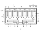
- FIG. 3 is a plan view showing an outline of the head substrate shown in FIG.
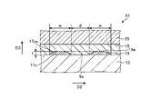
- FIG. 4 is a sectional view taken along line IV-IV of FIG.
- FIG. 5 is a cross-sectional view of a main part of the thermal head according to the reference embodiment.
- FIG. 6 is a cross-sectional view of a main part of the thermal head according to the first and second modifications of the embodiment.
- FIG. 7A is an enlarged cross-sectional view of the portion P1 shown in FIG.
- FIG. 7B is an enlarged cross-sectional view of the portion P2 shown in FIG. FIG.
- FIG. 8 is a cross-sectional view of a main part of the thermal head according to the third modification of the embodiment.
- FIG. 9 is a cross-sectional view of a main part of the thermal head according to the fourth modification of the embodiment.
- FIG. 10 is a cross-sectional view of a main part of the thermal head according to the fifth modification of the embodiment.
- FIG. 11 is a cross-sectional view of a main part of the thermal head according to the sixth modification of the embodiment.
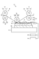
- FIG. 12 is a schematic diagram of the thermal printer according to the embodiment.
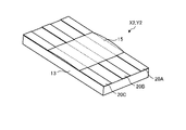
- FIG. 13A is a perspective view of the simulation model.
- 13B is a plan view of the simulation model shown in FIG. 13A.
- FIG. 14A is a side view of the simulation model shown in FIG. 13A as viewed from the long side.
- FIG. 13A is a perspective view of the simulation model. 13A as viewed from the long side.
- FIG. 14B is a side view of the simulation model of the thermal head according to the embodiment as viewed from the short side.
- FIG. 14C is a side view of the simulation model of the thermal head according to the reference embodiment as viewed from the short side.
- FIG. 15 is a table summarizing the physical property values used in the simulation.
- FIG. 16 is a graph showing the simulation results.
- FIG. 17A is a diagram showing a simulation result of the thermal head according to the embodiment.
- FIG. 17B is a diagram showing a simulation result of the thermal head according to the reference embodiment.
- the present disclosure has been made in view of the above, and provides a thermal head and a thermal printer capable of improving print image quality.
- FIG. 1 is a perspective view showing an outline of a thermal head according to an embodiment.
- the thermal head X1 according to the embodiment includes a heat radiating body 1, a head substrate 3, and an FPC (flexible printed wiring board) 5.
- the head substrate 3 is located on the radiator body 1.
- the FPC 5 is electrically connected to the head substrate 3.
- the head substrate 3 includes a substrate 7, a heat generating portion 9, a plurality of drive ICs 11, and a covering member 29.
- the radiator body 1 has a plate shape.
- the heat radiating body 1 has a rectangular shape in a plan view.
- the heat radiating body 1 has a heat radiating function. Specifically, the heat radiating body 1 releases the heat generated in the heat generating portion 9 of the head substrate 3 that does not contribute to the printing to the outside of the thermal head X1.
- the head substrate 3 is adhered to the upper surface of the heat radiating body 1 with double-sided tape, an adhesive or the like (not shown).
- the radiator 1 is made of a metal material such as copper, iron or aluminum.
- the head substrate 3 has a plate shape.
- the head substrate 3 has a rectangular shape in a plan view.
- each member constituting the thermal head X1 is located on the substrate 7.
- the head substrate 3 prints on the recording medium P (see FIG. 12) according to an electric signal supplied from the outside.
- the drive IC 11 is located on the substrate 7.
- the plurality of drive ICs 11 are located along the main scanning direction.
- the drive IC 11 is an electronic component having a function of controlling the energized state of each heat generating portion 9.
- a switching member having a plurality of switching elements inside may be used as the drive IC 11.
- the drive IC 11 is covered with a covering member 29 made of a resin such as an epoxy resin or a silicone resin.
- the covering member 29 is located across the plurality of drive ICs 11.
- the covering member 29 is an example of a sealing material.
- the FPC 5 has, for example, a pair of first and second ends in the lateral direction.
- the first end of the FPC 5 is electrically connected to the head substrate 3.
- the second end of the FPC 5 is electrically connected to the connector 31.
- the FPC 5 is electrically connected to the head substrate 3 by the conductive bonding material 23 (see FIG. 2).
- the conductive bonding material 23 As an example, an anisotropic conductive film (ACF) in which conductive particles are mixed in a solder material or an electrically insulating resin may be used as the conductive joining material 23.
- ACF anisotropic conductive film
- FIG. 2 is a cross-sectional view showing an outline of the thermal head shown in FIG.
- FIG. 3 is a plan view showing an outline of the head substrate shown in FIG.
- the head substrate 3 includes a substrate 7, a common electrode 17, an individual electrode 19, a third electrode 12, a fourth electrode 14, a terminal 2, a resistor layer 15, a protective layer 25, and a coating layer 27. Further prepare.
- the protective layer 25 and the covering layer 27 are omitted.
- FIG. 3 shows the wiring of the head substrate 3 in a simplified manner.
- the drive IC 11, the protective layer 25, and the covering layer 27 are omitted.
- the configuration of the fourth electrode 14 is simplified.
- the substrate 7 has a rectangular shape in a plan view, and the main surface (upper surface) 7e of the substrate 7 has a first long side 7a which is one long side and a second long side 7b which is the other long side. , The first short side 7c and the second short side 7d.
- the substrate 7 is made of an electrically insulating material such as alumina ceramics, a semiconductor material such as single crystal silicon, or the like.
- the substrate 7 may have a heat storage layer 13.
- the heat storage layer 13 is a portion that protrudes from the main surface 7e in the thickness direction of the substrate 7 and extends in a band shape along the second direction D2 (main scanning direction).
- the heat storage layer 13 has a function of satisfactorily pressing the recording medium for printing against the protective layer 25 located on the heat generating portion 9.
- the heat storage layer 13 may have a base portion.
- the base portion is a portion located over the entire area on the main surface 7e side of the substrate 7.
- the heat storage layer 13 contains, for example, a glass component.
- the heat storage layer 13 temporarily stores a part of the heat generated in the heat generating portion 9. As a result, the heat storage layer 13 can shorten the time required to raise the temperature of the heat generating portion 9. That is, the heat storage layer 13 has a function of enhancing the heat response characteristics of the thermal head X1.
- the heat storage layer 13 is produced, for example, by applying a predetermined glass paste obtained by mixing glass powder with an appropriate organic solvent to the main surface 7e side of the substrate 7 by screen printing or the like, which is well known in the past, and firing.
- the substrate 7 may have only a base portion as the heat storage layer 13.
- the common electrode 17 is located on the main surface 7e of the substrate 7.
- the common electrode 17 is made of a conductive material.
- any one of aluminum, gold, silver and copper or an alloy thereof may be used as the common electrode 17.
- the common electrode 17 has a first common electrode 17a, a plurality of second common electrodes 17b, a third common electrode 17c, and a plurality of terminals 2.
- the common electrode 17 is commonly and electrically connected to a plurality of elements included in the heat generating portion 9.
- the first common electrode 17a is located between the first long side 7a of the substrate 7 and the heat generating portion 9.
- the first common electrode 17a extends in the main scanning direction.
- the plurality of second common electrodes 17b extend in the sub-scanning direction.
- One of the plurality of (two in this case) second common electrodes 17b is located on the first short side 7c side of the substrate 7, and the other one is located on the second short side 7d side.
- the second common electrode 17b connects the terminal 2 and the first common electrode 17a.
- the third common electrode 17c extends from the first common electrode 17a toward each element of the heat generating portion 9 in a comb-teeth shape, and a part thereof is inserted through the opposite side of the heat generating portion 9.
- the third common electrode 17c is located at a distance from each other in the second direction D2 (main scanning direction).
- the third common electrode 17c is an example of the first electrode.
- the individual electrode 19 is located on the main surface 7e of the substrate 7.
- the individual electrode 19 contains a metal component and has conductivity.
- the individual electrode 19 is formed of, for example, metals such as aluminum, nickel, gold, silver, platinum, palladium, and copper, and alloys thereof.
- the plurality of individual electrodes 19 are located along the main scanning direction.
- the individual electrode 19 is located between two adjacent third common electrodes 17c. Therefore, in the thermal head X1, the third common electrode 17c and the individual electrodes 19 are alternately positioned in the main scanning direction.
- the individual electrode 19 has an electrode pad 10 connected to the second long side 7b side of the substrate 7.
- the individual electrode 19 is an example of the second electrode.
- the third electrode 12 is connected to the electrode pad 10.
- the third electrode 12 extends in the sub-scanning direction.
- the drive IC 11 is mounted on the electrode pad 10.
- the fourth electrode 14 extends in the main scanning direction.
- the fourth electrode 14 is located across the plurality of third electrodes 12.
- the fourth electrode 14 is connected to the outside by the terminal 2.
- the terminal 2 is located on the second long side 7b side of the substrate 7.
- the terminal 2 is connected to the FPC 5 by a conductive bonding material 23 (see FIG. 2).
- the head substrate 3 is electrically connected to the outside.
- the individual electrode 19, the third common electrode 17c, and the third electrode 12 for example, a conductor paste containing a metal component and a glass component in an organic solvent can be used as the electrode material.
- the individual electrodes 19, the third common electrode 17c, and the third electrode 12 each have a material layer formed on the substrate 7 by, for example, a screen printing method, a flexographic printing method, a gravure printing method, a gravure offset printing method, or the like. Can be made.
- the individual electrodes 19, the third common electrode 17c, and the third electrode 12 are sequentially laminated by, for example, a conventionally known thin film forming technique such as a sputtering method, and then the laminated body is predetermined by using a conventionally known photoetching or the like. It may be produced by processing into a pattern.
- the material layer constituting each of the first common electrode 17a, the second common electrode 17b, the fourth electrode 14, and the terminal 2 can be produced on the substrate 7 by, for example, a screen printing method.
- the thickness of the first common electrode 17a, the second common electrode 17b, the fourth electrode 14, and the terminal 2 is, for example, about 5 to 20 ⁇ m.
- the resistor layer 15 is located straddling the third common electrode 17c and the individual electrode 19 in a state of being separated from the first long side 7a of the substrate 7.
- the portion of the resistor layer 15 located between the third common electrode 17c and the individual electrode 19 functions as each element of the heat generating portion 9.
- each element of the heat generating portion 9 is shown in a simplified manner in FIG. 3, for example, it may be located at a density of 100 dpi (dots per inch) or more. Further, each element of the heat generating portion 9 may be located at a density of 200 to 2400 dpi.
- the thickness of the resistor layer 15 is, for example, about 3 to 6 ⁇ m.
- the sheet resistance of the resistor layer 15 is, for example, about 500 to 8000 ⁇ / ⁇ .
- the coefficient of thermal expansion of the resistor layer 15 is, for example, about 5 to 10 ppm / ° C.
- the thermal conductivity of the resistor layer 15 is, for example, about 0.5 to 2 W / (m ⁇ K).
- the resistor layer 15 is formed by, for example, arranging a material paste containing a conductive component and a glass component on a substrate 7 in which various electrodes are patterned in a long strip shape in the main scanning direction by a screen printing method, a dispensing device, or the like. May be formed by.
- the conductive component may include, for example, ruthenium oxide.
- the glass component may include, for example, lead borosilicate glass.
- the protective layer 25 is located on the heat storage layer 13 formed on the main surface 7e (see FIG. 1) of the substrate 7.
- the protective layer 25 covers the heat generating portion 9.
- the protective layer 25 is located in the main scanning direction of the substrate 7 so as to be separated from the electrode pad 10 from the first long side 7a of the substrate 7.
- the protective layer 25 has an insulating property. As a result, the protective layer 25 protects the covered area from corrosion due to adhesion of moisture and the like contained in the atmosphere, or wear due to contact with the recording medium to be printed.
- the protective layer 25 can be made of, for example, glass.
- the protective layer 25 can be manufactured by using, for example, a thick film forming technique such as printing.
- the protective layer 25 may contain, for example, lead borosilicate glass. Further, the protective layer 25 may further contain, for example, one or both of alumina and zirconia.
- the protective layer 25 may be made of SiN, SiON, SiO 2 , SiC, C—SiC, TiN, TiAlN, TiC, TiCN, TiSiN, CrN, DLC (diamond-like carbon) or the like.
- a protective layer 25 can be manufactured by using a thin film forming technique such as a sputtering method.
- the protective layer 25 may have, for example, a surface roughness Ra of 0.3 ⁇ m or less.
- the coating layer 27 is located on the substrate 7 so as to partially cover the common electrode 17, the individual electrode 19, the third electrode 12, and the fourth electrode 14.
- the covering layer 27 protects the covered region from oxidation due to contact with the atmosphere or corrosion due to adhesion of moisture or the like contained in the atmosphere.
- the coating layer 27 can be made of a resin material such as an epoxy resin, a polyimide resin, or a silicone resin.
- FIG. 4 is a sectional view taken along line IV-IV of FIG.
- the thermal head X1 has a heat storage layer 13, a third common electrode 17c, an individual electrode 19, a resistor layer 15, and a protective layer 25.
- the third common electrode 17c and the individual electrode 19 are located on the heat storage layer 13.
- the third common electrode 17c and the individual electrode 19 are located apart from each other by an interval d.
- the resistor layer 15 is located on the third common electrode 17c and the individual electrode 19, and on the heat storage layer 13 having no third common electrode 17c and the individual electrode 19.
- the third common electrode 17c and the individual electrode 19 are respectively positioned so as to be sandwiched between the heat storage layer 13 and the resistor layer 15.
- the protective layer 25 is positioned so as to cover the resistor layer 15.
- the cross-sectional shapes of the third common electrode 17c and the individual electrode 19 will be described.
- the central portion of the second direction D2 of the third common electrode 17c projects toward the third direction D3 side from the end portion of the second direction D2.
- the third direction D3 is a direction that intersects the first direction D1 (see FIG. 3) and the second direction D2.
- the central portion of the second direction D2 of the individual electrode 19 projects toward the third direction D3 side from the end portion of the second direction D2.
- the width w of the individual electrode 19 and the third common electrode 17c is, for example, about 10 to 50 ⁇ m. Further, the width w of the individual electrode 19 and the third common electrode 17c may be, for example, about 20 to 30 ⁇ m.
- the thickness t of the individual electrode 19 and the third common electrode 17c is, for example, about 0.5 to 5 ⁇ m. Further, the thickness t of the individual electrode 19 and the third common electrode 17c may be about 1 to 2 ⁇ m.
- the width w of the individual electrode 19 and the third common electrode 17c may be the same or different. Further, the thickness t of the individual electrode 19 and the third common electrode 17c may be the same or different.
- the thermal head X1 according to the embodiment is compared with the case where the upper surfaces 17ca and 19a of the individual electrodes 19 and the third common electrode 17c are flat so as to be along the first direction D1 (see FIG. 3) and the second direction D2. As a result, the image quality of the print is improved. This point will be further described with reference to FIGS. 4 and 5.
- FIG. 5 is a cross-sectional view of a main part of the thermal head according to the reference form.
- the thermal head Y1 according to the reference embodiment has the same configuration as the thermal head X1 shown in FIG. 4, except that the cross sections of the third common electrode 17c and the individual electrodes 19 are rectangular. ing.
- the thermal head X1 shown in FIG. 4 and the thermal head Y1 shown in FIG. 5 generate heat when a predetermined voltage is applied between the third common electrode 17c and the individual electrodes 19.
- the portion 9a of the resistor layer 15 having a substantially trapezoidal cross section sandwiched between the third common electrode 17c and the individual electrode 19 is the main heat generating portion. It becomes.
- the portion 9b of the resistor layer 15 having a substantially trapezoidal cross section sandwiched between the third common electrode 17c and the individual electrode 19 is the main heat generating portion.
- the portion 9a is cut off as compared with the portion 9b.
- the area and volume increase.
- the resistance values between the third common electrode 17c and the individual electrodes 19 are the same between the thermal heads X1 and Y1 in FIG.
- the thermal head X1 having a larger heat generating portion transfers heat to the resistor layer 15 away from the portion 9a as compared with the thermal head Y1. It will be easier.
- the temperature of the resistor layer 15 located above the central portion of the upper surface 17ca and the upper surface 19a in the second direction D2 that partition the adjacent heat generating portions 9 can be appropriately raised. ..
- the temperature difference between the portions on the upper surface of the resistor layer 15 becomes small.
- the connection of dots in the printed matter printed by the thermal head X1 is improved, and the print quality is improved.
- the third common electrode 17c and the individual electrode 19 in the thermal head X1 have the material layer constituting each of them on the substrate 7, for example, a screen printing method, a flexographic printing method, a gravure printing method, or a gravure offset printing method. It can be manufactured by such means. For example, a paste made from an intaglio having a desired groove shape is transferred to a bracket which is an intermediate support. Next, the paste is transferred again onto the heat storage layer 13 while appropriately adjusting the holding time and the pressing strength. Thereby, the material layer having a desired shape can be positioned on the substrate 7.
- the method for manufacturing the third common electrode 17c and the individual electrode 19 is not limited to the above, and the third common electrode 17c and the individual electrode 19 may be positioned by any method.
- FIG. 6 is a cross-sectional view of a main part of the thermal head according to the first and second modifications of the embodiment.
- the thermal head X1 is a resistor layer 15 located above the central portion in the width direction (second direction D2) of the third common electrode 17c (and the individual electrode 19).
- the thickness t1 of the resistor layer 15 is smaller than the thickness t2 of the resistor layer 15 located above the end portion of the second direction D2.
- FIG. 7A is an enlarged cross-sectional view of the portion P1 shown in FIG.
- FIG. 7B is an enlarged cross-sectional view of the portion P2 shown in FIG.
- the unevenness of the interface between the upper surface 17ca of the third common electrode 17c and the resistor layer 15 is the unevenness of the interface 13a between the resistor layer 15 and the heat storage layer 13 (see FIG. 7A). It may be larger than (see FIG. 7B).
- the unevenness of the interface in the photograph of the cross section, the height difference between the highest point and the lowest point in the region of 10 ⁇ m in length along the interface at an arbitrary place (the height difference between the most protruding part and the most recessed part). ) May be measured and used as the size of the unevenness of the interface.
- the magnitude of such unevenness can be visually discriminated based on, for example, an SEM (Scanning Electron Microscope) image.
- SEM Sccanning Electron Microscope
- the unevenness of the interface between the upper surface 19a of the individual electrode 19 and the resistor layer 15 can be made to be the same as the unevenness of the interface between the upper surface 17ca and the resistor layer 15. That is, the unevenness of the interface between the upper surface 19a and the resistor layer 15 may be larger than the unevenness of the interface between the resistor layer 15 and the heat storage layer 13.
- the unevenness of the interface between the resistor layer 15 and the heat storage layer 13 is made small, for example, the variation in the current path at the interface between the resistor layer 15 located in the region R2 and the heat storage layer 13 becomes small. Further, if the unevenness of the interface between the upper surface 17ca and the resistor layer 15 is increased, for example, the interface resistance between the upper surface 17ca located in the region R1 and the resistor layer 15 becomes smaller, and the variation in the interface resistance can be reduced. .. As a result, the variation in the resistance value between the electrodes adjacent to each other in the second direction D2 is reduced, and the density unevenness between the dots in the printed matter printed by the thermal head X1 can be reduced, so that the printing image quality is improved.
- FIG. 8 is a cross-sectional view of a main part of the thermal head according to the third modification of the embodiment.
- the thickness t3 of the protective layer 25 located on the third common electrode 17c (and the individual electrode 19) is the resistance layer 15 located between the third common electrode 17c and the individual electrode 19. It may be smaller than the thickness t4 of the protective layer 25 located above.
- the heat conduction distance to the surface of the protective layer 25 is reduced to the region R2. It is smaller than the heat conduction distance to the surface of the located protective layer 25. As a result, the temperature difference between the portions on the upper surface of the protective layer 25 becomes small. As a result, the connection of dots in the printed matter printed by the thermal head X1 is improved, and the print quality is improved.
- the protective layer 25 shown in FIG. 8 can be manufactured by the following procedure. That is, for example, a pattern having a portion where the material layer of the protective layer 25 is not located is formed on the resistor layer 15 located on the third common electrode 17c (and the individual electrode 19) by, for example, screen printing. After that, the protective layer 25 shown in FIG. 8 can be positioned on the resistor layer 15 by the softening flow of the material layer by firing.
- the method for producing the protective layer 25 is not limited, and the protective layer 25 may be positioned by any method.
- FIG. 9 is a cross-sectional view of a main part of the thermal head according to the fourth modification of the embodiment.
- the central portion of the second direction D2 protrudes from the end portion of the second direction D2 on the upper surfaces 17ca and 19a. Further, in the third common electrode 17c and the individual electrode 19, the central portion of the second direction D2 is negative in the third direction D3 with respect to the end portion of the second direction D2 on the lower surfaces 17ccb and 19b located above the heat storage layer 13. It may protrude to the direction side (heat storage layer 13 side).
- the amount of protrusion of the central portion with respect to the end portion in the second direction D2 is smaller on the lower surface 17cc than on the upper surface 17ca.
- the amount of protrusion of the central portion with respect to the end portion in the second direction D2 is smaller on the lower surface 19b than on the upper surface 19a.
- the thermal head X1 shown in FIG. 9 when a predetermined voltage is applied between the third common electrode 17c and the individual electrode 19, the resistor layer 15 sandwiched between the third common electrode 17c and the individual electrode 19
- the portion 9c is the main heat generation site. Since the amount of protrusion on the lower surfaces 17cab and 19b is smaller than the amount of protrusion on the upper surfaces 17ca and 19a, the amount of heat generated on the heat storage layer 13 side of the portion 9c located on the lower side opposite to the upper surface of the resistor layer 15 is increased. It can be made smaller. Further, the temperature on the upper surface side of the resistor layer 15 can be appropriately raised. As a result, the connection of dots in the printed matter printed by the thermal head X1 is improved, and the print quality is improved.
- the ratio (lower surface side protrusion amount / upper surface side protrusion amount) of the lower surface 17cc, 19b side protrusion amount (lower surface side protrusion amount) to the upper surface 17ca, 19a side protrusion amount (upper surface side protrusion amount) is, for example, 0. It can be .75 or less.
- the amount of protrusion on the lower surface side may be 0.
- the value of the amount of protrusion on the lower surface side / the amount of protrusion on the upper surface side is not limited to the above range.
- FIG. 10 is a cross-sectional view of a main part of the thermal head according to the fifth modification of the embodiment.
- the end portion 17ce of the third common electrode 17c in the second direction D2 protrudes in the second direction D2 from the end portion 17cc of the lower surface 17cc of the third common electrode 17c in the second direction D2. .. Further, the end portion 17cf of the third common electrode 17c located on the side opposite to the end portion 17ce is different from the end portion 17cd of the lower surface 17cc located on the side opposite to the end portion 17cc in the second direction D2. It protrudes to the other side.
- the end portion 19e of the second direction D2 of the individual electrode 19 protrudes in the second direction D2 from the end portion 19c of the lower surface 19b of the individual electrode 19 in the second direction.
- the end portion 19f of the individual electrode 19 located on the side opposite to the end portion 19e is on the side opposite to the second direction D2 with respect to the end portion 19d of the lower surface 19b located on the side opposite to the end portion 19c. It stands out.
- At least one of the third common electrode 17c and the individual electrode 19 has a portion closer to the upper surfaces 17ca and 19a than the lower surfaces 17cc and 19b so as to project toward the other of the third common electrode 17c and the individual electrodes 19.
- the portion of the other of the third common electrode 17c and the individual electrode 19 that is closer to the upper surfaces 17ca and 19a than the lower surfaces 17cc and 19b faces one of the third common electrode 17c and the individual electrode 19. It stands out, but it doesn't have to be.
- the end portions 17ce and 19e most protruding in the second direction D2 may be located apart from the lower surface 17cc and 19b in the third direction D3, respectively. good.
- the concentration point of the electric field generated between the third common electrode 17c and the individual electrode 19 by energization approaches the central portion in the thickness direction (third direction D3) of the resistor layer 15.
- the ratio of the portion located inside the resistor layer 15 to the electric field generated between the third common electrode 17c and the individual electrode 19 increases, so that the heat generation efficiency of the resistor layer 15 is improved.
- FIG. 11 is a cross-sectional view of a main part of the thermal head according to the sixth modification of the embodiment.
- the thermal head X1 shown in FIG. 11 differs from the thermal head X1 according to the embodiment in that it has a first protective layer 25a and a second protective layer 25b instead of the protective layer 25.
- the first protective layer 25a is located on the resistor layer 15.
- the first protective layer 25a can be made of, for example, glass.
- the first protective layer 25a may contain, for example, lead borosilicate glass. Further, the first protective layer 25a may further contain, for example, one or both of alumina and zirconia.
- the first protective layer 25a has an insulating property. As a result, the first protective layer 25a is protected from corrosion due to adhesion of moisture and the like contained in the atmosphere.
- the second protective layer 25b is located on the first protective layer 25a.
- the second protective layer 25b may be made of, for example, SiN, SiON, SiO 2 , SiC, C—SiC, TiN, TiAlN, TiC, TiCN, TiSiN, CrN, DLC, or the like.
- the second protective layer 25b has an insulating property. As a result, the second protective layer 25b is protected from corrosion due to adhesion of moisture and the like contained in the atmosphere, or wear due to contact with the recording medium to be printed.
- FIG. 12 is a schematic diagram of the thermal printer according to the embodiment.
- the thermal printer Z1 includes the above-mentioned thermal head X1, a transport mechanism 40, a platen roller 50, a power supply device 60, and a control device 70.
- the thermal head X1 is attached to a mounting surface 80a of a mounting member 80 arranged in a housing (not shown) of the thermal printer Z1.
- the thermal head X1 is attached to the mounting member 80 so as to be along the main scanning direction which is a direction orthogonal to the transport direction S.
- the transport mechanism 40 has a drive unit (not shown) and transport rollers 43, 45, 47, 49.
- the transport mechanism 40 is on the protective layer 25 located on the plurality of heat generating portions 9 of the thermal head X1 so that the recording medium P such as the thermal paper and the image receiving paper on which the ink is transferred is along the transport direction S indicated by the arrow.
- the drive unit has a function of driving the transfer rollers 43, 45, 47, 49.
- a motor may be used as a drive unit.
- the transport rollers 43, 45, 47, 49 are made of, for example, columnar shaft bodies 43a, 45a, 47a, 49a made of a metal such as stainless steel, and elastic members 43b, 45b, 47b, made of butadiene rubber or the like. It may be covered with 49b.
- an ink film (not shown) is conveyed between the recording medium P and the heat generating portion 9 of the thermal head X1 together with the recording medium P.
- the platen roller 50 has a function of pressing the recording medium P onto the protective layer 25 located on the heat generating portion 9 of the thermal head X1.
- the platen roller 50 is arranged so as to extend along a direction orthogonal to the transport direction S, and both ends thereof are supported and fixed so as to be rotatable while the recording medium P is pressed onto the heat generating portion 9.
- the platen roller 50 may be configured by, for example, covering a columnar shaft body 50a made of a metal such as stainless steel with an elastic member 50b made of butadiene rubber or the like.
- the power supply device 60 has a function of supplying a current for heating the heat generating portion 9 of the thermal head X1 and a current for operating the drive IC 11.
- the control device 70 has a function of supplying a control signal for controlling the operation of the drive IC 11 to the drive IC 11 in order to selectively generate heat of the heat generation unit 9 of the thermal head X1 as described above.
- the thermal printer Z1 presses the recording medium P onto the heat generating portion 9 of the thermal head X1 by the platen roller 50, and conveys the recording medium P onto the heat generating portion 9 by the conveying mechanism 40, while the power supply device 60 and the control device 70. Selectively heats the heat generating unit 9 by. As a result, the thermal printer Z1 prints a predetermined image on the recording medium P.
- the recording medium P is an image receiving paper or the like
- the ink of the ink film (not shown) conveyed together with the recording medium P is thermally transferred to the recording medium P to print on the recording medium P.
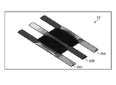
- FIG. 13A is a perspective view of the simulation model.
- 13B is a plan view of the simulation model shown in FIG. 13A.
- FIG. 14A is a side view of the simulation model shown in FIG. 13A as viewed from the long side.
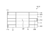
- FIG. 14B is a side view of the simulation model X2 as viewed from the short side.
- FIG. 14C is a side view of the simulation model Y2 as viewed from the short side.
- the simulation models X2 and Y2 have a heat storage layer 13, electrodes 20A to 20C located on the heat storage layer 13, and a resistor layer 15 that covers a part of the heat storage layer 13 and the electrodes 20A to 20C. ..
- the electrodes 20A to 20C may be simply referred to as electrodes 20.
- the electrode 20A, the electrode 20C, and the electrode 20B one corresponds to the first electrode and the other corresponds to the second electrode.
- the electrodes 20A to 20C extend along the long side S1 of the heat storage layer 13.
- the electrodes 20A to 20C are arranged side by side at equal intervals in the short side S2 direction.
- Each of the electrodes 20A to 20C has a width of 26 ⁇ m and a thickness of 1 ⁇ m.
- the maximum height of the resistor layer 15 from the heat storage layer 13 is 6 ⁇ m.
- the resistor layer 15 covers the central portion of the heat storage layer 13 and the electrodes 20A to 20C in the length direction of each.
- the maximum width of the resistor layer 15 is 130 ⁇ m.
- the simulation model X2 has a curved surface shape in which the upper surface 20a of the electrode 20 has a protruding center in the width direction. That is, in the simulation model X2, on the upper surface 20a of the electrode 20, the central portion in the short side S2 direction protrudes from the end portion in the short side S2 direction.
- the simulation model Y2 differs from the simulation model X2 in that the cross section of the electrode 20 has a rectangular shape, as shown in FIG. 14C.
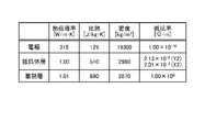
- FIG. 15 is a table summarizing the physical property values used in the simulation.
- FIG. 15 shows the values of thermal conductivity, specific heat, density and resistivity of the electrode 20, the resistor layer 15 and the heat storage layer 13.
- the resistivity values of the resistors are slightly different between the simulation models Y2 and X2. This is because the resistance value between the first electrode and the second electrode (to be exact, the resistance value between the parts P11 and P13 and the part P12 in FIG. 13B) is the simulation models Y2 and X2. This is because they were adjusted to be equal.
- FIGS. 17A and 17B are diagrams showing the calorific value of each part.
- the portion having a large calorific value is shown in a dark color.
- the simulation model X2 it can be seen that in the simulation model X2, the portion having a large amount of heat generation extends toward the center in the width direction of the electrodes 20A to 20C as compared with the simulation model Y2.
- the vicinity of the electrode 20B located in the center is in the state closest to the real thing.
- FIG. 16 is a graph showing the temperature on the upper surface of the resistor layer 15, and shows the temperature of the portion shown by MP in FIG. 13B. According to FIG. 16, it can be seen that in the simulation model X2, the temperature of the portion located on the electrode 20B on the upper surface of the resistor layer 15 is higher than that in the simulation model Y2.
- the present invention is effective for improving the printing quality of the thermal head.
- the present disclosure is not limited to the above embodiments, and various changes can be made as long as the purpose is not deviated.
- the two or more third common electrodes 17c and the individual electrodes 19 according to the embodiment and each modification may be appropriately combined.
- only one of the third common electrode 17c and the individual electrode 19 may be used as the third common electrode 17c or the individual electrode 19 according to the embodiment and each modification.
- the thermal head X1 for example, a flat head in which the heat generating portion 9, the heat storage layer 13, the common electrode 17, the individual electrode 19, and the like are located on the main surface 7e of the substrate 7 is exemplified.
- the heat generating portion 9, the heat storage layer 13, the common electrode 17, the individual electrode 19, and the like may be located on a surface other than the main surface 7e of the substrate 7.
- the description has been made using a so-called thick film head in which the resistor layer 15 is formed by printing, the description is not limited to the thick film head.
- the resistor layer 15 may be used for a so-called thin film head formed by sputtering.
- the connector 31 may be directly electrically connected to the head substrate 3 without providing the FPC 5.
- the connector pin (not shown) of the connector 31 and the electrode pad 10 may be electrically connected.
- the thermal head X1 having the covering layer 27 is exemplified, the covering layer 27 does not necessarily have to be provided. In that case, the protective layer 25 (or the first protective layer 25a and the second protective layer 25b) may be extended to the region where the covering layer 27 is provided.
Landscapes
- Physics & Mathematics (AREA)
- Geometry (AREA)
- Electronic Switches (AREA)
Priority Applications (4)
| Application Number | Priority Date | Filing Date | Title |
|---|---|---|---|
| US18/028,214 US20230373226A1 (en) | 2020-09-30 | 2021-09-28 | Thermal head and thermal printer |
| CN202180064233.6A CN116323232B (zh) | 2020-09-30 | 2021-09-28 | 热敏头以及热敏打印机 |
| JP2022554031A JP7454696B2 (ja) | 2020-09-30 | 2021-09-28 | サーマルヘッドおよびサーマルプリンタ |
| EP21875648.4A EP4223544A4 (en) | 2020-09-30 | 2021-09-28 | THERMAL HEAD AND THERMAL PRINTER |
Applications Claiming Priority (2)
| Application Number | Priority Date | Filing Date | Title |
|---|---|---|---|
| JP2020-166488 | 2020-09-30 | ||
| JP2020166488 | 2020-09-30 |
Publications (1)
| Publication Number | Publication Date |
|---|---|
| WO2022071347A1 true WO2022071347A1 (ja) | 2022-04-07 |
Family
ID=80950581
Family Applications (1)
| Application Number | Title | Priority Date | Filing Date |
|---|---|---|---|
| PCT/JP2021/035716 Ceased WO2022071347A1 (ja) | 2020-09-30 | 2021-09-28 | サーマルヘッドおよびサーマルプリンタ |
Country Status (5)
| Country | Link |
|---|---|
| US (1) | US20230373226A1 (https=) |
| EP (1) | EP4223544A4 (https=) |
| JP (1) | JP7454696B2 (https=) |
| CN (1) | CN116323232B (https=) |
| WO (1) | WO2022071347A1 (https=) |
Families Citing this family (1)
| Publication number | Priority date | Publication date | Assignee | Title |
|---|---|---|---|---|
| USD936139S1 (en) * | 2018-02-28 | 2021-11-16 | Sato Holdings Kabushiki Kaisha | Thermal head for a printer |
Citations (7)
| Publication number | Priority date | Publication date | Assignee | Title |
|---|---|---|---|---|
| JPS5499443A (en) | 1978-01-23 | 1979-08-06 | Hitachi Ltd | Forming method of heating resistors of thick film type heat sensitive recording head |
| JPS60145863A (ja) * | 1984-01-10 | 1985-08-01 | Oki Electric Ind Co Ltd | 薄膜サ−マルヘツド |
| JPH029641A (ja) * | 1988-06-29 | 1990-01-12 | Hitachi Ltd | 感熱記録ヘッド |
| JPH02182468A (ja) * | 1989-01-09 | 1990-07-17 | Oki Electric Ind Co Ltd | サーマルヘッドの電極部構造 |
| US20060232656A1 (en) * | 2005-04-15 | 2006-10-19 | Eastman Kodak Company | Thermal printer, print head, printing method and substrate for use therewith |
| JP2018192694A (ja) * | 2017-05-17 | 2018-12-06 | ローム株式会社 | サーマルプリントヘッドおよびサーマルプリントヘッドの製造方法 |
| JP2019119149A (ja) | 2018-01-09 | 2019-07-22 | ローム株式会社 | サーマルプリントヘッド |
Family Cites Families (15)
| Publication number | Priority date | Publication date | Assignee | Title |
|---|---|---|---|---|
| JPH0834133A (ja) * | 1994-07-22 | 1996-02-06 | Rohm Co Ltd | サーマルヘッドおよびこれを用いたプリンタ |
| JP3794105B2 (ja) * | 1997-05-19 | 2006-07-05 | 神鋼電機株式会社 | サーマルヘッド |
| US6891331B2 (en) * | 2000-08-30 | 2005-05-10 | Matsushita Electric Industrial Co., Ltd. | Plasma display unit and production method thereof |
| JP4434016B2 (ja) * | 2002-08-02 | 2010-03-17 | 日本碍子株式会社 | 圧電/電歪膜型素子の製造方法 |
| JP4367771B2 (ja) * | 2004-06-15 | 2009-11-18 | ローム株式会社 | サーマルヘッド |
| JP5329887B2 (ja) * | 2008-09-26 | 2013-10-30 | 東芝ホクト電子株式会社 | サーマルヘッド |
| US9238376B2 (en) * | 2011-11-28 | 2016-01-19 | Kyocera Corporation | Thermal head and thermal printer equipped with the same |
| JP5952089B2 (ja) * | 2012-01-25 | 2016-07-13 | ローム株式会社 | 微細配線パターンの製造方法、およびサーマルプリントヘッド |
| CN104619504B (zh) * | 2012-09-28 | 2017-05-03 | 京瓷株式会社 | 热敏头以及具备该热敏头的热敏打印机 |
| US9937728B2 (en) * | 2014-08-26 | 2018-04-10 | Kyocera Corporation | Thermal head and thermal printer |
| JP2016137692A (ja) * | 2015-01-29 | 2016-08-04 | 京セラ株式会社 | サーマルヘッドおよびこれを備えるサーマルプリンタ |
| JP6364383B2 (ja) * | 2015-06-30 | 2018-07-25 | アオイ電子株式会社 | 配線基板、およびサーマルヘッド |
| JP2019164993A (ja) * | 2018-03-14 | 2019-09-26 | 株式会社リコー | 電極形成用組成物、電極の製造方法及び非水系蓄電素子の製造方法 |
| JP2020151890A (ja) * | 2019-03-19 | 2020-09-24 | 東芝ホクト電子株式会社 | サーマルプリントヘッド及びサーマルプリンタ |
| TWI708690B (zh) * | 2019-07-01 | 2020-11-01 | 謙華科技股份有限公司 | 能夠提高輸出解析度的熱印頭結構及其製造方法 |
-
2021
- 2021-09-28 JP JP2022554031A patent/JP7454696B2/ja active Active
- 2021-09-28 CN CN202180064233.6A patent/CN116323232B/zh active Active
- 2021-09-28 EP EP21875648.4A patent/EP4223544A4/en active Pending
- 2021-09-28 WO PCT/JP2021/035716 patent/WO2022071347A1/ja not_active Ceased
- 2021-09-28 US US18/028,214 patent/US20230373226A1/en active Pending
Patent Citations (7)
| Publication number | Priority date | Publication date | Assignee | Title |
|---|---|---|---|---|
| JPS5499443A (en) | 1978-01-23 | 1979-08-06 | Hitachi Ltd | Forming method of heating resistors of thick film type heat sensitive recording head |
| JPS60145863A (ja) * | 1984-01-10 | 1985-08-01 | Oki Electric Ind Co Ltd | 薄膜サ−マルヘツド |
| JPH029641A (ja) * | 1988-06-29 | 1990-01-12 | Hitachi Ltd | 感熱記録ヘッド |
| JPH02182468A (ja) * | 1989-01-09 | 1990-07-17 | Oki Electric Ind Co Ltd | サーマルヘッドの電極部構造 |
| US20060232656A1 (en) * | 2005-04-15 | 2006-10-19 | Eastman Kodak Company | Thermal printer, print head, printing method and substrate for use therewith |
| JP2018192694A (ja) * | 2017-05-17 | 2018-12-06 | ローム株式会社 | サーマルプリントヘッドおよびサーマルプリントヘッドの製造方法 |
| JP2019119149A (ja) | 2018-01-09 | 2019-07-22 | ローム株式会社 | サーマルプリントヘッド |
Non-Patent Citations (1)
| Title |
|---|
| See also references of EP4223544A4 |
Also Published As
| Publication number | Publication date |
|---|---|
| EP4223544A1 (en) | 2023-08-09 |
| JP7454696B2 (ja) | 2024-03-22 |
| EP4223544A4 (en) | 2024-11-06 |
| CN116323232A (zh) | 2023-06-23 |
| US20230373226A1 (en) | 2023-11-23 |
| JPWO2022071347A1 (https=) | 2022-04-07 |
| CN116323232B (zh) | 2026-04-21 |
Similar Documents
| Publication | Publication Date | Title |
|---|---|---|
| JP6181244B2 (ja) | サーマルヘッドおよびこれを備えるサーマルプリンタ | |
| JP5836825B2 (ja) | サーマルヘッドおよびこれを備えるサーマルプリンタ | |
| JP7454696B2 (ja) | サーマルヘッドおよびサーマルプリンタ | |
| CN115298037B (zh) | 热敏头以及热敏打印机 | |
| JP7336588B2 (ja) | サーマルヘッドおよびサーマルプリンタ | |
| JP2012030439A (ja) | サーマルヘッドおよびこれを備えるサーマルプリンタ | |
| CN105408119B (zh) | 热敏头及具备该热敏头的热敏打印机 | |
| JP7444972B2 (ja) | サーマルヘッドおよびサーマルプリンタ | |
| JP2016185675A (ja) | サーマルヘッドおよびサーマルプリンタ | |
| JP7411461B2 (ja) | サーマルヘッドおよびサーマルプリンタ | |
| JP2016137692A (ja) | サーマルヘッドおよびこれを備えるサーマルプリンタ | |
| JPWO2017170800A1 (ja) | サーマルヘッドおよびサーマルプリンタ | |
| WO2025244111A1 (ja) | サーマルヘッドおよびサーマルプリンタ | |
| WO2025243860A1 (ja) | サーマルヘッドおよびサーマルプリンタ | |
| JP7811998B2 (ja) | サーマルヘッドおよびサーマルプリンタ | |
| JP4369723B2 (ja) | サーマルヘッド、及びそれを用いたサーマルプリンタ | |
| JP7036692B2 (ja) | サーマルヘッドおよびサーマルプリンタ | |
| JP5918049B2 (ja) | サーマルヘッドおよびこれを備えるサーマルプリンタ | |
| JP6901419B2 (ja) | サーマルヘッドおよびサーマルプリンタ | |
| JP6426541B2 (ja) | サーマルヘッドおよびサーマルプリンタ | |
| JPWO2020067424A1 (ja) | サーマルヘッドおよびサーマルプリンタ | |
| JP2021107142A (ja) | サーマルヘッドおよびサーマルプリンタ |
Legal Events
| Date | Code | Title | Description |
|---|---|---|---|
| 121 | Ep: the epo has been informed by wipo that ep was designated in this application |
Ref document number: 21875648 Country of ref document: EP Kind code of ref document: A1 |
|
| ENP | Entry into the national phase |
Ref document number: 2022554031 Country of ref document: JP Kind code of ref document: A |
|
| NENP | Non-entry into the national phase |
Ref country code: DE |
|
| ENP | Entry into the national phase |
Ref document number: 2021875648 Country of ref document: EP Effective date: 20230502 |