WO2022071347A1 - サーマルヘッドおよびサーマルプリンタ - Google Patents
サーマルヘッドおよびサーマルプリンタ Download PDFInfo
- Publication number
- WO2022071347A1 WO2022071347A1 PCT/JP2021/035716 JP2021035716W WO2022071347A1 WO 2022071347 A1 WO2022071347 A1 WO 2022071347A1 JP 2021035716 W JP2021035716 W JP 2021035716W WO 2022071347 A1 WO2022071347 A1 WO 2022071347A1
- Authority
- WO
- WIPO (PCT)
- Prior art keywords
- electrode
- thermal head
- substrate
- layer
- resistor layer
- Prior art date
Links
- 239000000758 substrate Substances 0.000 claims abstract description 65
- 239000010410 layer Substances 0.000 claims description 115
- 239000011241 protective layer Substances 0.000 claims description 53
- 238000005338 heat storage Methods 0.000 claims description 35
- 230000032258 transport Effects 0.000 claims description 8
- 230000007723 transport mechanism Effects 0.000 claims description 6
- 238000004088 simulation Methods 0.000 description 34
- 230000004048 modification Effects 0.000 description 21
- 238000012986 modification Methods 0.000 description 21
- 238000000034 method Methods 0.000 description 17
- 239000000463 material Substances 0.000 description 13
- 238000007639 printing Methods 0.000 description 9
- 239000011521 glass Substances 0.000 description 8
- 239000010408 film Substances 0.000 description 6
- 238000007650 screen-printing Methods 0.000 description 6
- 238000010586 diagram Methods 0.000 description 5
- 229910052751 metal Inorganic materials 0.000 description 5
- 239000002184 metal Substances 0.000 description 5
- MCMNRKCIXSYSNV-UHFFFAOYSA-N Zirconium dioxide Chemical compound O=[Zr]=O MCMNRKCIXSYSNV-UHFFFAOYSA-N 0.000 description 4
- 239000011247 coating layer Substances 0.000 description 4
- 238000005260 corrosion Methods 0.000 description 4
- 230000007797 corrosion Effects 0.000 description 4
- 230000020169 heat generation Effects 0.000 description 4
- RYGMFSIKBFXOCR-UHFFFAOYSA-N Copper Chemical compound [Cu] RYGMFSIKBFXOCR-UHFFFAOYSA-N 0.000 description 3
- 229910052782 aluminium Inorganic materials 0.000 description 3
- XAGFODPZIPBFFR-UHFFFAOYSA-N aluminium Chemical compound [Al] XAGFODPZIPBFFR-UHFFFAOYSA-N 0.000 description 3
- PNEYBMLMFCGWSK-UHFFFAOYSA-N aluminium oxide Inorganic materials [O-2].[O-2].[O-2].[Al+3].[Al+3] PNEYBMLMFCGWSK-UHFFFAOYSA-N 0.000 description 3
- 239000005388 borosilicate glass Substances 0.000 description 3
- 229910052802 copper Inorganic materials 0.000 description 3
- 239000010949 copper Substances 0.000 description 3
- 238000003825 pressing Methods 0.000 description 3
- 229920005989 resin Polymers 0.000 description 3
- 239000011347 resin Substances 0.000 description 3
- 238000004544 sputter deposition Methods 0.000 description 3
- 239000010409 thin film Substances 0.000 description 3
- XEEYBQQBJWHFJM-UHFFFAOYSA-N Iron Chemical compound [Fe] XEEYBQQBJWHFJM-UHFFFAOYSA-N 0.000 description 2
- PXHVJJICTQNCMI-UHFFFAOYSA-N Nickel Chemical compound [Ni] PXHVJJICTQNCMI-UHFFFAOYSA-N 0.000 description 2
- KDLHZDBZIXYQEI-UHFFFAOYSA-N Palladium Chemical compound [Pd] KDLHZDBZIXYQEI-UHFFFAOYSA-N 0.000 description 2
- 239000005062 Polybutadiene Substances 0.000 description 2
- 229910004541 SiN Inorganic materials 0.000 description 2
- 229910004298 SiO 2 Inorganic materials 0.000 description 2
- BQCADISMDOOEFD-UHFFFAOYSA-N Silver Chemical compound [Ag] BQCADISMDOOEFD-UHFFFAOYSA-N 0.000 description 2
- 229910010037 TiAlN Inorganic materials 0.000 description 2
- 229910008482 TiSiN Inorganic materials 0.000 description 2
- ATJFFYVFTNAWJD-UHFFFAOYSA-N Tin Chemical compound [Sn] ATJFFYVFTNAWJD-UHFFFAOYSA-N 0.000 description 2
- 229910045601 alloy Inorganic materials 0.000 description 2
- 239000000956 alloy Substances 0.000 description 2
- 239000004020 conductor Substances 0.000 description 2
- 230000000694 effects Effects 0.000 description 2
- 230000005684 electric field Effects 0.000 description 2
- 239000003822 epoxy resin Substances 0.000 description 2
- 238000010304 firing Methods 0.000 description 2
- PCHJSUWPFVWCPO-UHFFFAOYSA-N gold Chemical compound [Au] PCHJSUWPFVWCPO-UHFFFAOYSA-N 0.000 description 2
- 229910052737 gold Inorganic materials 0.000 description 2
- 239000010931 gold Substances 0.000 description 2
- 238000007646 gravure printing Methods 0.000 description 2
- QRXWMOHMRWLFEY-UHFFFAOYSA-N isoniazide Chemical compound NNC(=O)C1=CC=NC=C1 QRXWMOHMRWLFEY-UHFFFAOYSA-N 0.000 description 2
- 238000004519 manufacturing process Methods 0.000 description 2
- 229910003465 moissanite Inorganic materials 0.000 description 2
- 238000007645 offset printing Methods 0.000 description 2
- 239000003960 organic solvent Substances 0.000 description 2
- 230000000704 physical effect Effects 0.000 description 2
- BASFCYQUMIYNBI-UHFFFAOYSA-N platinum Chemical compound [Pt] BASFCYQUMIYNBI-UHFFFAOYSA-N 0.000 description 2
- 229920002857 polybutadiene Polymers 0.000 description 2
- 229920000647 polyepoxide Polymers 0.000 description 2
- 229910010271 silicon carbide Inorganic materials 0.000 description 2
- 229910052814 silicon oxide Inorganic materials 0.000 description 2
- 229920002050 silicone resin Polymers 0.000 description 2
- 229910052709 silver Inorganic materials 0.000 description 2
- 239000004332 silver Substances 0.000 description 2
- 239000010935 stainless steel Substances 0.000 description 2
- 229910001220 stainless steel Inorganic materials 0.000 description 2
- 238000012546 transfer Methods 0.000 description 2
- OKTJSMMVPCPJKN-UHFFFAOYSA-N Carbon Chemical compound [C] OKTJSMMVPCPJKN-UHFFFAOYSA-N 0.000 description 1
- 239000000853 adhesive Substances 0.000 description 1
- 230000001070 adhesive effect Effects 0.000 description 1
- 238000013459 approach Methods 0.000 description 1
- 229910052799 carbon Inorganic materials 0.000 description 1
- 239000000919 ceramic Substances 0.000 description 1
- 239000011248 coating agent Substances 0.000 description 1
- 238000000576 coating method Methods 0.000 description 1
- 239000012777 electrically insulating material Substances 0.000 description 1
- 239000007772 electrode material Substances 0.000 description 1
- 230000002708 enhancing effect Effects 0.000 description 1
- 238000010438 heat treatment Methods 0.000 description 1
- 230000006872 improvement Effects 0.000 description 1
- 229910052742 iron Inorganic materials 0.000 description 1
- 230000007246 mechanism Effects 0.000 description 1
- 239000007769 metal material Substances 0.000 description 1
- 150000002739 metals Chemical class 0.000 description 1
- 229910021421 monocrystalline silicon Inorganic materials 0.000 description 1
- 229910052759 nickel Inorganic materials 0.000 description 1
- 230000003647 oxidation Effects 0.000 description 1
- 238000007254 oxidation reaction Methods 0.000 description 1
- 229910052763 palladium Inorganic materials 0.000 description 1
- 239000002245 particle Substances 0.000 description 1
- 238000005192 partition Methods 0.000 description 1
- 238000001259 photo etching Methods 0.000 description 1
- 229910052697 platinum Inorganic materials 0.000 description 1
- 229920001721 polyimide Polymers 0.000 description 1
- 239000009719 polyimide resin Substances 0.000 description 1
- 239000000843 powder Substances 0.000 description 1
- 238000012545 processing Methods 0.000 description 1
- 230000004044 response Effects 0.000 description 1
- 229910001925 ruthenium oxide Inorganic materials 0.000 description 1
- WOCIAKWEIIZHES-UHFFFAOYSA-N ruthenium(iv) oxide Chemical compound O=[Ru]=O WOCIAKWEIIZHES-UHFFFAOYSA-N 0.000 description 1
- 239000003566 sealing material Substances 0.000 description 1
- 239000004065 semiconductor Substances 0.000 description 1
- 239000002356 single layer Substances 0.000 description 1
- 229910000679 solder Inorganic materials 0.000 description 1
- 230000003746 surface roughness Effects 0.000 description 1
Images


Classifications
-
- B—PERFORMING OPERATIONS; TRANSPORTING
- B41—PRINTING; LINING MACHINES; TYPEWRITERS; STAMPS
- B41J—TYPEWRITERS; SELECTIVE PRINTING MECHANISMS, i.e. MECHANISMS PRINTING OTHERWISE THAN FROM A FORME; CORRECTION OF TYPOGRAPHICAL ERRORS
- B41J2/00—Typewriters or selective printing mechanisms characterised by the printing or marking process for which they are designed
- B41J2/315—Typewriters or selective printing mechanisms characterised by the printing or marking process for which they are designed characterised by selective application of heat to a heat sensitive printing or impression-transfer material
- B41J2/32—Typewriters or selective printing mechanisms characterised by the printing or marking process for which they are designed characterised by selective application of heat to a heat sensitive printing or impression-transfer material using thermal heads
- B41J2/335—Structure of thermal heads
- B41J2/33505—Constructional details
- B41J2/3351—Electrode layers
-
- B—PERFORMING OPERATIONS; TRANSPORTING
- B41—PRINTING; LINING MACHINES; TYPEWRITERS; STAMPS
- B41J—TYPEWRITERS; SELECTIVE PRINTING MECHANISMS, i.e. MECHANISMS PRINTING OTHERWISE THAN FROM A FORME; CORRECTION OF TYPOGRAPHICAL ERRORS
- B41J2/00—Typewriters or selective printing mechanisms characterised by the printing or marking process for which they are designed
- B41J2/315—Typewriters or selective printing mechanisms characterised by the printing or marking process for which they are designed characterised by selective application of heat to a heat sensitive printing or impression-transfer material
- B41J2/32—Typewriters or selective printing mechanisms characterised by the printing or marking process for which they are designed characterised by selective application of heat to a heat sensitive printing or impression-transfer material using thermal heads
- B41J2/345—Typewriters or selective printing mechanisms characterised by the printing or marking process for which they are designed characterised by selective application of heat to a heat sensitive printing or impression-transfer material using thermal heads characterised by the arrangement of resistors or conductors
-
- B—PERFORMING OPERATIONS; TRANSPORTING
- B41—PRINTING; LINING MACHINES; TYPEWRITERS; STAMPS
- B41J—TYPEWRITERS; SELECTIVE PRINTING MECHANISMS, i.e. MECHANISMS PRINTING OTHERWISE THAN FROM A FORME; CORRECTION OF TYPOGRAPHICAL ERRORS
- B41J2/00—Typewriters or selective printing mechanisms characterised by the printing or marking process for which they are designed
- B41J2/315—Typewriters or selective printing mechanisms characterised by the printing or marking process for which they are designed characterised by selective application of heat to a heat sensitive printing or impression-transfer material
- B41J2/32—Typewriters or selective printing mechanisms characterised by the printing or marking process for which they are designed characterised by selective application of heat to a heat sensitive printing or impression-transfer material using thermal heads
- B41J2/335—Structure of thermal heads
- B41J2/33505—Constructional details
- B41J2/33525—Passivation layers
-
- B—PERFORMING OPERATIONS; TRANSPORTING
- B41—PRINTING; LINING MACHINES; TYPEWRITERS; STAMPS
- B41J—TYPEWRITERS; SELECTIVE PRINTING MECHANISMS, i.e. MECHANISMS PRINTING OTHERWISE THAN FROM A FORME; CORRECTION OF TYPOGRAPHICAL ERRORS
- B41J2/00—Typewriters or selective printing mechanisms characterised by the printing or marking process for which they are designed
- B41J2/315—Typewriters or selective printing mechanisms characterised by the printing or marking process for which they are designed characterised by selective application of heat to a heat sensitive printing or impression-transfer material
- B41J2/32—Typewriters or selective printing mechanisms characterised by the printing or marking process for which they are designed characterised by selective application of heat to a heat sensitive printing or impression-transfer material using thermal heads
- B41J2/335—Structure of thermal heads
- B41J2/33505—Constructional details
- B41J2/3353—Protective layers
-
- B—PERFORMING OPERATIONS; TRANSPORTING
- B41—PRINTING; LINING MACHINES; TYPEWRITERS; STAMPS
- B41J—TYPEWRITERS; SELECTIVE PRINTING MECHANISMS, i.e. MECHANISMS PRINTING OTHERWISE THAN FROM A FORME; CORRECTION OF TYPOGRAPHICAL ERRORS
- B41J2/00—Typewriters or selective printing mechanisms characterised by the printing or marking process for which they are designed
- B41J2/315—Typewriters or selective printing mechanisms characterised by the printing or marking process for which they are designed characterised by selective application of heat to a heat sensitive printing or impression-transfer material
- B41J2/32—Typewriters or selective printing mechanisms characterised by the printing or marking process for which they are designed characterised by selective application of heat to a heat sensitive printing or impression-transfer material using thermal heads
- B41J2/335—Structure of thermal heads
- B41J2/3354—Structure of thermal heads characterised by geometry
-
- B—PERFORMING OPERATIONS; TRANSPORTING
- B41—PRINTING; LINING MACHINES; TYPEWRITERS; STAMPS
- B41J—TYPEWRITERS; SELECTIVE PRINTING MECHANISMS, i.e. MECHANISMS PRINTING OTHERWISE THAN FROM A FORME; CORRECTION OF TYPOGRAPHICAL ERRORS
- B41J2/00—Typewriters or selective printing mechanisms characterised by the printing or marking process for which they are designed
- B41J2/315—Typewriters or selective printing mechanisms characterised by the printing or marking process for which they are designed characterised by selective application of heat to a heat sensitive printing or impression-transfer material
- B41J2/32—Typewriters or selective printing mechanisms characterised by the printing or marking process for which they are designed characterised by selective application of heat to a heat sensitive printing or impression-transfer material using thermal heads
- B41J2/335—Structure of thermal heads
- B41J2/3355—Structure of thermal heads characterised by materials
-
- B—PERFORMING OPERATIONS; TRANSPORTING
- B41—PRINTING; LINING MACHINES; TYPEWRITERS; STAMPS
- B41J—TYPEWRITERS; SELECTIVE PRINTING MECHANISMS, i.e. MECHANISMS PRINTING OTHERWISE THAN FROM A FORME; CORRECTION OF TYPOGRAPHICAL ERRORS
- B41J2/00—Typewriters or selective printing mechanisms characterised by the printing or marking process for which they are designed
- B41J2/315—Typewriters or selective printing mechanisms characterised by the printing or marking process for which they are designed characterised by selective application of heat to a heat sensitive printing or impression-transfer material
- B41J2/32—Typewriters or selective printing mechanisms characterised by the printing or marking process for which they are designed characterised by selective application of heat to a heat sensitive printing or impression-transfer material using thermal heads
- B41J2/335—Structure of thermal heads
- B41J2/33555—Structure of thermal heads characterised by type
- B41J2/3357—Surface type resistors
Definitions
- the embodiment of the disclosure relates to a thermal head and a thermal printer.
- the thermal head includes a substrate, electrodes, and a resistor layer.
- the electrodes are located on the substrate and extend along a first direction of the substrate.
- the resistor layer is located on the substrate and on the electrodes.
- the electrode has a first electrode and a second electrode arranged at predetermined intervals in a second direction intersecting the first direction. At least one of the first electrode and the second electrode has a central portion in the second direction protruding from an end portion in the second direction on an upper surface located below the resistor layer.
- the thermal printer includes the thermal head described above, a transport mechanism, and a platen roller.
- the transport mechanism transports the recording medium onto the heat generating portion located on the substrate.
- the platen roller presses the recording medium onto the heat generating portion.
- FIG. 1 is a perspective view showing an outline of a thermal head according to an embodiment.
- FIG. 2 is a cross-sectional view showing an outline of the thermal head shown in FIG.
- FIG. 3 is a plan view showing an outline of the head substrate shown in FIG.
- FIG. 4 is a sectional view taken along line IV-IV of FIG.
- FIG. 5 is a cross-sectional view of a main part of the thermal head according to the reference embodiment.
- FIG. 6 is a cross-sectional view of a main part of the thermal head according to the first and second modifications of the embodiment.
- FIG. 7A is an enlarged cross-sectional view of the portion P1 shown in FIG.
- FIG. 7B is an enlarged cross-sectional view of the portion P2 shown in FIG. FIG.
- FIG. 8 is a cross-sectional view of a main part of the thermal head according to the third modification of the embodiment.
- FIG. 9 is a cross-sectional view of a main part of the thermal head according to the fourth modification of the embodiment.
- FIG. 10 is a cross-sectional view of a main part of the thermal head according to the fifth modification of the embodiment.
- FIG. 11 is a cross-sectional view of a main part of the thermal head according to the sixth modification of the embodiment.
- FIG. 12 is a schematic diagram of the thermal printer according to the embodiment.
- FIG. 13A is a perspective view of the simulation model.
- 13B is a plan view of the simulation model shown in FIG. 13A.
- FIG. 14A is a side view of the simulation model shown in FIG. 13A as viewed from the long side.
- FIG. 13A is a perspective view of the simulation model. 13A as viewed from the long side.
- FIG. 14B is a side view of the simulation model of the thermal head according to the embodiment as viewed from the short side.
- FIG. 14C is a side view of the simulation model of the thermal head according to the reference embodiment as viewed from the short side.
- FIG. 15 is a table summarizing the physical property values used in the simulation.
- FIG. 16 is a graph showing the simulation results.
- FIG. 17A is a diagram showing a simulation result of the thermal head according to the embodiment.
- FIG. 17B is a diagram showing a simulation result of the thermal head according to the reference embodiment.
- the present disclosure has been made in view of the above, and provides a thermal head and a thermal printer capable of improving print image quality.
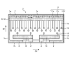
- FIG. 1 is a perspective view showing an outline of a thermal head according to an embodiment.
- the thermal head X1 according to the embodiment includes a heat radiating body 1, a head substrate 3, and an FPC (flexible printed wiring board) 5.
- the head substrate 3 is located on the radiator body 1.
- the FPC 5 is electrically connected to the head substrate 3.
- the head substrate 3 includes a substrate 7, a heat generating portion 9, a plurality of drive ICs 11, and a covering member 29.
- the radiator body 1 has a plate shape.
- the heat radiating body 1 has a rectangular shape in a plan view.
- the heat radiating body 1 has a heat radiating function. Specifically, the heat radiating body 1 releases the heat generated in the heat generating portion 9 of the head substrate 3 that does not contribute to the printing to the outside of the thermal head X1.
- the head substrate 3 is adhered to the upper surface of the heat radiating body 1 with double-sided tape, an adhesive or the like (not shown).
- the radiator 1 is made of a metal material such as copper, iron or aluminum.
- the head substrate 3 has a plate shape.
- the head substrate 3 has a rectangular shape in a plan view.
- each member constituting the thermal head X1 is located on the substrate 7.
- the head substrate 3 prints on the recording medium P (see FIG. 12) according to an electric signal supplied from the outside.
- the drive IC 11 is located on the substrate 7.
- the plurality of drive ICs 11 are located along the main scanning direction.
- the drive IC 11 is an electronic component having a function of controlling the energized state of each heat generating portion 9.
- a switching member having a plurality of switching elements inside may be used as the drive IC 11.
- the drive IC 11 is covered with a covering member 29 made of a resin such as an epoxy resin or a silicone resin.
- the covering member 29 is located across the plurality of drive ICs 11.
- the covering member 29 is an example of a sealing material.
- the FPC 5 has, for example, a pair of first and second ends in the lateral direction.
- the first end of the FPC 5 is electrically connected to the head substrate 3.
- the second end of the FPC 5 is electrically connected to the connector 31.
- the FPC 5 is electrically connected to the head substrate 3 by the conductive bonding material 23 (see FIG. 2).
- the conductive bonding material 23 As an example, an anisotropic conductive film (ACF) in which conductive particles are mixed in a solder material or an electrically insulating resin may be used as the conductive joining material 23.
- ACF anisotropic conductive film
- FIG. 2 is a cross-sectional view showing an outline of the thermal head shown in FIG.
- FIG. 3 is a plan view showing an outline of the head substrate shown in FIG.
- the head substrate 3 includes a substrate 7, a common electrode 17, an individual electrode 19, a third electrode 12, a fourth electrode 14, a terminal 2, a resistor layer 15, a protective layer 25, and a coating layer 27. Further prepare.
- the protective layer 25 and the covering layer 27 are omitted.
- FIG. 3 shows the wiring of the head substrate 3 in a simplified manner.
- the drive IC 11, the protective layer 25, and the covering layer 27 are omitted.
- the configuration of the fourth electrode 14 is simplified.
- the substrate 7 has a rectangular shape in a plan view, and the main surface (upper surface) 7e of the substrate 7 has a first long side 7a which is one long side and a second long side 7b which is the other long side. , The first short side 7c and the second short side 7d.
- the substrate 7 is made of an electrically insulating material such as alumina ceramics, a semiconductor material such as single crystal silicon, or the like.
- the substrate 7 may have a heat storage layer 13.
- the heat storage layer 13 is a portion that protrudes from the main surface 7e in the thickness direction of the substrate 7 and extends in a band shape along the second direction D2 (main scanning direction).
- the heat storage layer 13 has a function of satisfactorily pressing the recording medium for printing against the protective layer 25 located on the heat generating portion 9.
- the heat storage layer 13 may have a base portion.
- the base portion is a portion located over the entire area on the main surface 7e side of the substrate 7.
- the heat storage layer 13 contains, for example, a glass component.
- the heat storage layer 13 temporarily stores a part of the heat generated in the heat generating portion 9. As a result, the heat storage layer 13 can shorten the time required to raise the temperature of the heat generating portion 9. That is, the heat storage layer 13 has a function of enhancing the heat response characteristics of the thermal head X1.
- the heat storage layer 13 is produced, for example, by applying a predetermined glass paste obtained by mixing glass powder with an appropriate organic solvent to the main surface 7e side of the substrate 7 by screen printing or the like, which is well known in the past, and firing.
- the substrate 7 may have only a base portion as the heat storage layer 13.
- the common electrode 17 is located on the main surface 7e of the substrate 7.
- the common electrode 17 is made of a conductive material.
- any one of aluminum, gold, silver and copper or an alloy thereof may be used as the common electrode 17.
- the common electrode 17 has a first common electrode 17a, a plurality of second common electrodes 17b, a third common electrode 17c, and a plurality of terminals 2.
- the common electrode 17 is commonly and electrically connected to a plurality of elements included in the heat generating portion 9.
- the first common electrode 17a is located between the first long side 7a of the substrate 7 and the heat generating portion 9.
- the first common electrode 17a extends in the main scanning direction.
- the plurality of second common electrodes 17b extend in the sub-scanning direction.
- One of the plurality of (two in this case) second common electrodes 17b is located on the first short side 7c side of the substrate 7, and the other one is located on the second short side 7d side.
- the second common electrode 17b connects the terminal 2 and the first common electrode 17a.
- the third common electrode 17c extends from the first common electrode 17a toward each element of the heat generating portion 9 in a comb-teeth shape, and a part thereof is inserted through the opposite side of the heat generating portion 9.
- the third common electrode 17c is located at a distance from each other in the second direction D2 (main scanning direction).
- the third common electrode 17c is an example of the first electrode.
- the individual electrode 19 is located on the main surface 7e of the substrate 7.
- the individual electrode 19 contains a metal component and has conductivity.
- the individual electrode 19 is formed of, for example, metals such as aluminum, nickel, gold, silver, platinum, palladium, and copper, and alloys thereof.
- the plurality of individual electrodes 19 are located along the main scanning direction.
- the individual electrode 19 is located between two adjacent third common electrodes 17c. Therefore, in the thermal head X1, the third common electrode 17c and the individual electrodes 19 are alternately positioned in the main scanning direction.
- the individual electrode 19 has an electrode pad 10 connected to the second long side 7b side of the substrate 7.
- the individual electrode 19 is an example of the second electrode.
- the third electrode 12 is connected to the electrode pad 10.
- the third electrode 12 extends in the sub-scanning direction.
- the drive IC 11 is mounted on the electrode pad 10.
- the fourth electrode 14 extends in the main scanning direction.
- the fourth electrode 14 is located across the plurality of third electrodes 12.
- the fourth electrode 14 is connected to the outside by the terminal 2.
- the terminal 2 is located on the second long side 7b side of the substrate 7.
- the terminal 2 is connected to the FPC 5 by a conductive bonding material 23 (see FIG. 2).
- the head substrate 3 is electrically connected to the outside.
- the individual electrode 19, the third common electrode 17c, and the third electrode 12 for example, a conductor paste containing a metal component and a glass component in an organic solvent can be used as the electrode material.
- the individual electrodes 19, the third common electrode 17c, and the third electrode 12 each have a material layer formed on the substrate 7 by, for example, a screen printing method, a flexographic printing method, a gravure printing method, a gravure offset printing method, or the like. Can be made.
- the individual electrodes 19, the third common electrode 17c, and the third electrode 12 are sequentially laminated by, for example, a conventionally known thin film forming technique such as a sputtering method, and then the laminated body is predetermined by using a conventionally known photoetching or the like. It may be produced by processing into a pattern.
- the material layer constituting each of the first common electrode 17a, the second common electrode 17b, the fourth electrode 14, and the terminal 2 can be produced on the substrate 7 by, for example, a screen printing method.
- the thickness of the first common electrode 17a, the second common electrode 17b, the fourth electrode 14, and the terminal 2 is, for example, about 5 to 20 ⁇ m.
- the resistor layer 15 is located straddling the third common electrode 17c and the individual electrode 19 in a state of being separated from the first long side 7a of the substrate 7.
- the portion of the resistor layer 15 located between the third common electrode 17c and the individual electrode 19 functions as each element of the heat generating portion 9.
- each element of the heat generating portion 9 is shown in a simplified manner in FIG. 3, for example, it may be located at a density of 100 dpi (dots per inch) or more. Further, each element of the heat generating portion 9 may be located at a density of 200 to 2400 dpi.
- the thickness of the resistor layer 15 is, for example, about 3 to 6 ⁇ m.
- the sheet resistance of the resistor layer 15 is, for example, about 500 to 8000 ⁇ / ⁇ .
- the coefficient of thermal expansion of the resistor layer 15 is, for example, about 5 to 10 ppm / ° C.
- the thermal conductivity of the resistor layer 15 is, for example, about 0.5 to 2 W / (m ⁇ K).
- the resistor layer 15 is formed by, for example, arranging a material paste containing a conductive component and a glass component on a substrate 7 in which various electrodes are patterned in a long strip shape in the main scanning direction by a screen printing method, a dispensing device, or the like. May be formed by.
- the conductive component may include, for example, ruthenium oxide.
- the glass component may include, for example, lead borosilicate glass.
- the protective layer 25 is located on the heat storage layer 13 formed on the main surface 7e (see FIG. 1) of the substrate 7.
- the protective layer 25 covers the heat generating portion 9.
- the protective layer 25 is located in the main scanning direction of the substrate 7 so as to be separated from the electrode pad 10 from the first long side 7a of the substrate 7.
- the protective layer 25 has an insulating property. As a result, the protective layer 25 protects the covered area from corrosion due to adhesion of moisture and the like contained in the atmosphere, or wear due to contact with the recording medium to be printed.
- the protective layer 25 can be made of, for example, glass.
- the protective layer 25 can be manufactured by using, for example, a thick film forming technique such as printing.
- the protective layer 25 may contain, for example, lead borosilicate glass. Further, the protective layer 25 may further contain, for example, one or both of alumina and zirconia.
- the protective layer 25 may be made of SiN, SiON, SiO 2 , SiC, C—SiC, TiN, TiAlN, TiC, TiCN, TiSiN, CrN, DLC (diamond-like carbon) or the like.
- a protective layer 25 can be manufactured by using a thin film forming technique such as a sputtering method.
- the protective layer 25 may have, for example, a surface roughness Ra of 0.3 ⁇ m or less.
- the coating layer 27 is located on the substrate 7 so as to partially cover the common electrode 17, the individual electrode 19, the third electrode 12, and the fourth electrode 14.
- the covering layer 27 protects the covered region from oxidation due to contact with the atmosphere or corrosion due to adhesion of moisture or the like contained in the atmosphere.
- the coating layer 27 can be made of a resin material such as an epoxy resin, a polyimide resin, or a silicone resin.
- FIG. 4 is a sectional view taken along line IV-IV of FIG.
- the thermal head X1 has a heat storage layer 13, a third common electrode 17c, an individual electrode 19, a resistor layer 15, and a protective layer 25.
- the third common electrode 17c and the individual electrode 19 are located on the heat storage layer 13.
- the third common electrode 17c and the individual electrode 19 are located apart from each other by an interval d.
- the resistor layer 15 is located on the third common electrode 17c and the individual electrode 19, and on the heat storage layer 13 having no third common electrode 17c and the individual electrode 19.
- the third common electrode 17c and the individual electrode 19 are respectively positioned so as to be sandwiched between the heat storage layer 13 and the resistor layer 15.
- the protective layer 25 is positioned so as to cover the resistor layer 15.
- the cross-sectional shapes of the third common electrode 17c and the individual electrode 19 will be described.
- the central portion of the second direction D2 of the third common electrode 17c projects toward the third direction D3 side from the end portion of the second direction D2.
- the third direction D3 is a direction that intersects the first direction D1 (see FIG. 3) and the second direction D2.
- the central portion of the second direction D2 of the individual electrode 19 projects toward the third direction D3 side from the end portion of the second direction D2.
- the width w of the individual electrode 19 and the third common electrode 17c is, for example, about 10 to 50 ⁇ m. Further, the width w of the individual electrode 19 and the third common electrode 17c may be, for example, about 20 to 30 ⁇ m.
- the thickness t of the individual electrode 19 and the third common electrode 17c is, for example, about 0.5 to 5 ⁇ m. Further, the thickness t of the individual electrode 19 and the third common electrode 17c may be about 1 to 2 ⁇ m.
- the width w of the individual electrode 19 and the third common electrode 17c may be the same or different. Further, the thickness t of the individual electrode 19 and the third common electrode 17c may be the same or different.
- the thermal head X1 according to the embodiment is compared with the case where the upper surfaces 17ca and 19a of the individual electrodes 19 and the third common electrode 17c are flat so as to be along the first direction D1 (see FIG. 3) and the second direction D2. As a result, the image quality of the print is improved. This point will be further described with reference to FIGS. 4 and 5.
- FIG. 5 is a cross-sectional view of a main part of the thermal head according to the reference form.
- the thermal head Y1 according to the reference embodiment has the same configuration as the thermal head X1 shown in FIG. 4, except that the cross sections of the third common electrode 17c and the individual electrodes 19 are rectangular. ing.
- the thermal head X1 shown in FIG. 4 and the thermal head Y1 shown in FIG. 5 generate heat when a predetermined voltage is applied between the third common electrode 17c and the individual electrodes 19.
- the portion 9a of the resistor layer 15 having a substantially trapezoidal cross section sandwiched between the third common electrode 17c and the individual electrode 19 is the main heat generating portion. It becomes.
- the portion 9b of the resistor layer 15 having a substantially trapezoidal cross section sandwiched between the third common electrode 17c and the individual electrode 19 is the main heat generating portion.
- the portion 9a is cut off as compared with the portion 9b.
- the area and volume increase.
- the resistance values between the third common electrode 17c and the individual electrodes 19 are the same between the thermal heads X1 and Y1 in FIG.
- the thermal head X1 having a larger heat generating portion transfers heat to the resistor layer 15 away from the portion 9a as compared with the thermal head Y1. It will be easier.
- the temperature of the resistor layer 15 located above the central portion of the upper surface 17ca and the upper surface 19a in the second direction D2 that partition the adjacent heat generating portions 9 can be appropriately raised. ..
- the temperature difference between the portions on the upper surface of the resistor layer 15 becomes small.
- the connection of dots in the printed matter printed by the thermal head X1 is improved, and the print quality is improved.
- the third common electrode 17c and the individual electrode 19 in the thermal head X1 have the material layer constituting each of them on the substrate 7, for example, a screen printing method, a flexographic printing method, a gravure printing method, or a gravure offset printing method. It can be manufactured by such means. For example, a paste made from an intaglio having a desired groove shape is transferred to a bracket which is an intermediate support. Next, the paste is transferred again onto the heat storage layer 13 while appropriately adjusting the holding time and the pressing strength. Thereby, the material layer having a desired shape can be positioned on the substrate 7.
- the method for manufacturing the third common electrode 17c and the individual electrode 19 is not limited to the above, and the third common electrode 17c and the individual electrode 19 may be positioned by any method.
- FIG. 6 is a cross-sectional view of a main part of the thermal head according to the first and second modifications of the embodiment.
- the thermal head X1 is a resistor layer 15 located above the central portion in the width direction (second direction D2) of the third common electrode 17c (and the individual electrode 19).
- the thickness t1 of the resistor layer 15 is smaller than the thickness t2 of the resistor layer 15 located above the end portion of the second direction D2.
- FIG. 7A is an enlarged cross-sectional view of the portion P1 shown in FIG.
- FIG. 7B is an enlarged cross-sectional view of the portion P2 shown in FIG.
- the unevenness of the interface between the upper surface 17ca of the third common electrode 17c and the resistor layer 15 is the unevenness of the interface 13a between the resistor layer 15 and the heat storage layer 13 (see FIG. 7A). It may be larger than (see FIG. 7B).
- the unevenness of the interface in the photograph of the cross section, the height difference between the highest point and the lowest point in the region of 10 ⁇ m in length along the interface at an arbitrary place (the height difference between the most protruding part and the most recessed part). ) May be measured and used as the size of the unevenness of the interface.
- the magnitude of such unevenness can be visually discriminated based on, for example, an SEM (Scanning Electron Microscope) image.
- SEM Sccanning Electron Microscope
- the unevenness of the interface between the upper surface 19a of the individual electrode 19 and the resistor layer 15 can be made to be the same as the unevenness of the interface between the upper surface 17ca and the resistor layer 15. That is, the unevenness of the interface between the upper surface 19a and the resistor layer 15 may be larger than the unevenness of the interface between the resistor layer 15 and the heat storage layer 13.
- the unevenness of the interface between the resistor layer 15 and the heat storage layer 13 is made small, for example, the variation in the current path at the interface between the resistor layer 15 located in the region R2 and the heat storage layer 13 becomes small. Further, if the unevenness of the interface between the upper surface 17ca and the resistor layer 15 is increased, for example, the interface resistance between the upper surface 17ca located in the region R1 and the resistor layer 15 becomes smaller, and the variation in the interface resistance can be reduced. .. As a result, the variation in the resistance value between the electrodes adjacent to each other in the second direction D2 is reduced, and the density unevenness between the dots in the printed matter printed by the thermal head X1 can be reduced, so that the printing image quality is improved.
- FIG. 8 is a cross-sectional view of a main part of the thermal head according to the third modification of the embodiment.
- the thickness t3 of the protective layer 25 located on the third common electrode 17c (and the individual electrode 19) is the resistance layer 15 located between the third common electrode 17c and the individual electrode 19. It may be smaller than the thickness t4 of the protective layer 25 located above.
- the heat conduction distance to the surface of the protective layer 25 is reduced to the region R2. It is smaller than the heat conduction distance to the surface of the located protective layer 25. As a result, the temperature difference between the portions on the upper surface of the protective layer 25 becomes small. As a result, the connection of dots in the printed matter printed by the thermal head X1 is improved, and the print quality is improved.
- the protective layer 25 shown in FIG. 8 can be manufactured by the following procedure. That is, for example, a pattern having a portion where the material layer of the protective layer 25 is not located is formed on the resistor layer 15 located on the third common electrode 17c (and the individual electrode 19) by, for example, screen printing. After that, the protective layer 25 shown in FIG. 8 can be positioned on the resistor layer 15 by the softening flow of the material layer by firing.
- the method for producing the protective layer 25 is not limited, and the protective layer 25 may be positioned by any method.
- FIG. 9 is a cross-sectional view of a main part of the thermal head according to the fourth modification of the embodiment.
- the central portion of the second direction D2 protrudes from the end portion of the second direction D2 on the upper surfaces 17ca and 19a. Further, in the third common electrode 17c and the individual electrode 19, the central portion of the second direction D2 is negative in the third direction D3 with respect to the end portion of the second direction D2 on the lower surfaces 17ccb and 19b located above the heat storage layer 13. It may protrude to the direction side (heat storage layer 13 side).
- the amount of protrusion of the central portion with respect to the end portion in the second direction D2 is smaller on the lower surface 17cc than on the upper surface 17ca.
- the amount of protrusion of the central portion with respect to the end portion in the second direction D2 is smaller on the lower surface 19b than on the upper surface 19a.
- the thermal head X1 shown in FIG. 9 when a predetermined voltage is applied between the third common electrode 17c and the individual electrode 19, the resistor layer 15 sandwiched between the third common electrode 17c and the individual electrode 19
- the portion 9c is the main heat generation site. Since the amount of protrusion on the lower surfaces 17cab and 19b is smaller than the amount of protrusion on the upper surfaces 17ca and 19a, the amount of heat generated on the heat storage layer 13 side of the portion 9c located on the lower side opposite to the upper surface of the resistor layer 15 is increased. It can be made smaller. Further, the temperature on the upper surface side of the resistor layer 15 can be appropriately raised. As a result, the connection of dots in the printed matter printed by the thermal head X1 is improved, and the print quality is improved.
- the ratio (lower surface side protrusion amount / upper surface side protrusion amount) of the lower surface 17cc, 19b side protrusion amount (lower surface side protrusion amount) to the upper surface 17ca, 19a side protrusion amount (upper surface side protrusion amount) is, for example, 0. It can be .75 or less.
- the amount of protrusion on the lower surface side may be 0.
- the value of the amount of protrusion on the lower surface side / the amount of protrusion on the upper surface side is not limited to the above range.
- FIG. 10 is a cross-sectional view of a main part of the thermal head according to the fifth modification of the embodiment.
- the end portion 17ce of the third common electrode 17c in the second direction D2 protrudes in the second direction D2 from the end portion 17cc of the lower surface 17cc of the third common electrode 17c in the second direction D2. .. Further, the end portion 17cf of the third common electrode 17c located on the side opposite to the end portion 17ce is different from the end portion 17cd of the lower surface 17cc located on the side opposite to the end portion 17cc in the second direction D2. It protrudes to the other side.
- the end portion 19e of the second direction D2 of the individual electrode 19 protrudes in the second direction D2 from the end portion 19c of the lower surface 19b of the individual electrode 19 in the second direction.
- the end portion 19f of the individual electrode 19 located on the side opposite to the end portion 19e is on the side opposite to the second direction D2 with respect to the end portion 19d of the lower surface 19b located on the side opposite to the end portion 19c. It stands out.
- At least one of the third common electrode 17c and the individual electrode 19 has a portion closer to the upper surfaces 17ca and 19a than the lower surfaces 17cc and 19b so as to project toward the other of the third common electrode 17c and the individual electrodes 19.
- the portion of the other of the third common electrode 17c and the individual electrode 19 that is closer to the upper surfaces 17ca and 19a than the lower surfaces 17cc and 19b faces one of the third common electrode 17c and the individual electrode 19. It stands out, but it doesn't have to be.
- the end portions 17ce and 19e most protruding in the second direction D2 may be located apart from the lower surface 17cc and 19b in the third direction D3, respectively. good.
- the concentration point of the electric field generated between the third common electrode 17c and the individual electrode 19 by energization approaches the central portion in the thickness direction (third direction D3) of the resistor layer 15.
- the ratio of the portion located inside the resistor layer 15 to the electric field generated between the third common electrode 17c and the individual electrode 19 increases, so that the heat generation efficiency of the resistor layer 15 is improved.
- FIG. 11 is a cross-sectional view of a main part of the thermal head according to the sixth modification of the embodiment.
- the thermal head X1 shown in FIG. 11 differs from the thermal head X1 according to the embodiment in that it has a first protective layer 25a and a second protective layer 25b instead of the protective layer 25.
- the first protective layer 25a is located on the resistor layer 15.
- the first protective layer 25a can be made of, for example, glass.
- the first protective layer 25a may contain, for example, lead borosilicate glass. Further, the first protective layer 25a may further contain, for example, one or both of alumina and zirconia.
- the first protective layer 25a has an insulating property. As a result, the first protective layer 25a is protected from corrosion due to adhesion of moisture and the like contained in the atmosphere.
- the second protective layer 25b is located on the first protective layer 25a.
- the second protective layer 25b may be made of, for example, SiN, SiON, SiO 2 , SiC, C—SiC, TiN, TiAlN, TiC, TiCN, TiSiN, CrN, DLC, or the like.
- the second protective layer 25b has an insulating property. As a result, the second protective layer 25b is protected from corrosion due to adhesion of moisture and the like contained in the atmosphere, or wear due to contact with the recording medium to be printed.
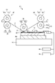
- FIG. 12 is a schematic diagram of the thermal printer according to the embodiment.
- the thermal printer Z1 includes the above-mentioned thermal head X1, a transport mechanism 40, a platen roller 50, a power supply device 60, and a control device 70.
- the thermal head X1 is attached to a mounting surface 80a of a mounting member 80 arranged in a housing (not shown) of the thermal printer Z1.
- the thermal head X1 is attached to the mounting member 80 so as to be along the main scanning direction which is a direction orthogonal to the transport direction S.
- the transport mechanism 40 has a drive unit (not shown) and transport rollers 43, 45, 47, 49.
- the transport mechanism 40 is on the protective layer 25 located on the plurality of heat generating portions 9 of the thermal head X1 so that the recording medium P such as the thermal paper and the image receiving paper on which the ink is transferred is along the transport direction S indicated by the arrow.
- the drive unit has a function of driving the transfer rollers 43, 45, 47, 49.
- a motor may be used as a drive unit.
- the transport rollers 43, 45, 47, 49 are made of, for example, columnar shaft bodies 43a, 45a, 47a, 49a made of a metal such as stainless steel, and elastic members 43b, 45b, 47b, made of butadiene rubber or the like. It may be covered with 49b.
- an ink film (not shown) is conveyed between the recording medium P and the heat generating portion 9 of the thermal head X1 together with the recording medium P.
- the platen roller 50 has a function of pressing the recording medium P onto the protective layer 25 located on the heat generating portion 9 of the thermal head X1.
- the platen roller 50 is arranged so as to extend along a direction orthogonal to the transport direction S, and both ends thereof are supported and fixed so as to be rotatable while the recording medium P is pressed onto the heat generating portion 9.
- the platen roller 50 may be configured by, for example, covering a columnar shaft body 50a made of a metal such as stainless steel with an elastic member 50b made of butadiene rubber or the like.
- the power supply device 60 has a function of supplying a current for heating the heat generating portion 9 of the thermal head X1 and a current for operating the drive IC 11.
- the control device 70 has a function of supplying a control signal for controlling the operation of the drive IC 11 to the drive IC 11 in order to selectively generate heat of the heat generation unit 9 of the thermal head X1 as described above.
- the thermal printer Z1 presses the recording medium P onto the heat generating portion 9 of the thermal head X1 by the platen roller 50, and conveys the recording medium P onto the heat generating portion 9 by the conveying mechanism 40, while the power supply device 60 and the control device 70. Selectively heats the heat generating unit 9 by. As a result, the thermal printer Z1 prints a predetermined image on the recording medium P.
- the recording medium P is an image receiving paper or the like
- the ink of the ink film (not shown) conveyed together with the recording medium P is thermally transferred to the recording medium P to print on the recording medium P.
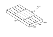
- FIG. 13A is a perspective view of the simulation model.
- 13B is a plan view of the simulation model shown in FIG. 13A.
- FIG. 14A is a side view of the simulation model shown in FIG. 13A as viewed from the long side.
- FIG. 14B is a side view of the simulation model X2 as viewed from the short side.
- FIG. 14C is a side view of the simulation model Y2 as viewed from the short side.
- the simulation models X2 and Y2 have a heat storage layer 13, electrodes 20A to 20C located on the heat storage layer 13, and a resistor layer 15 that covers a part of the heat storage layer 13 and the electrodes 20A to 20C. ..
- the electrodes 20A to 20C may be simply referred to as electrodes 20.
- the electrode 20A, the electrode 20C, and the electrode 20B one corresponds to the first electrode and the other corresponds to the second electrode.
- the electrodes 20A to 20C extend along the long side S1 of the heat storage layer 13.
- the electrodes 20A to 20C are arranged side by side at equal intervals in the short side S2 direction.
- Each of the electrodes 20A to 20C has a width of 26 ⁇ m and a thickness of 1 ⁇ m.
- the maximum height of the resistor layer 15 from the heat storage layer 13 is 6 ⁇ m.
- the resistor layer 15 covers the central portion of the heat storage layer 13 and the electrodes 20A to 20C in the length direction of each.
- the maximum width of the resistor layer 15 is 130 ⁇ m.
- the simulation model X2 has a curved surface shape in which the upper surface 20a of the electrode 20 has a protruding center in the width direction. That is, in the simulation model X2, on the upper surface 20a of the electrode 20, the central portion in the short side S2 direction protrudes from the end portion in the short side S2 direction.
- the simulation model Y2 differs from the simulation model X2 in that the cross section of the electrode 20 has a rectangular shape, as shown in FIG. 14C.
- FIG. 15 is a table summarizing the physical property values used in the simulation.
- FIG. 15 shows the values of thermal conductivity, specific heat, density and resistivity of the electrode 20, the resistor layer 15 and the heat storage layer 13.
- the resistivity values of the resistors are slightly different between the simulation models Y2 and X2. This is because the resistance value between the first electrode and the second electrode (to be exact, the resistance value between the parts P11 and P13 and the part P12 in FIG. 13B) is the simulation models Y2 and X2. This is because they were adjusted to be equal.
- FIGS. 17A and 17B are diagrams showing the calorific value of each part.
- the portion having a large calorific value is shown in a dark color.
- the simulation model X2 it can be seen that in the simulation model X2, the portion having a large amount of heat generation extends toward the center in the width direction of the electrodes 20A to 20C as compared with the simulation model Y2.
- the vicinity of the electrode 20B located in the center is in the state closest to the real thing.
- FIG. 16 is a graph showing the temperature on the upper surface of the resistor layer 15, and shows the temperature of the portion shown by MP in FIG. 13B. According to FIG. 16, it can be seen that in the simulation model X2, the temperature of the portion located on the electrode 20B on the upper surface of the resistor layer 15 is higher than that in the simulation model Y2.
- the present invention is effective for improving the printing quality of the thermal head.
- the present disclosure is not limited to the above embodiments, and various changes can be made as long as the purpose is not deviated.
- the two or more third common electrodes 17c and the individual electrodes 19 according to the embodiment and each modification may be appropriately combined.
- only one of the third common electrode 17c and the individual electrode 19 may be used as the third common electrode 17c or the individual electrode 19 according to the embodiment and each modification.
- the thermal head X1 for example, a flat head in which the heat generating portion 9, the heat storage layer 13, the common electrode 17, the individual electrode 19, and the like are located on the main surface 7e of the substrate 7 is exemplified.
- the heat generating portion 9, the heat storage layer 13, the common electrode 17, the individual electrode 19, and the like may be located on a surface other than the main surface 7e of the substrate 7.
- the description has been made using a so-called thick film head in which the resistor layer 15 is formed by printing, the description is not limited to the thick film head.
- the resistor layer 15 may be used for a so-called thin film head formed by sputtering.
- the connector 31 may be directly electrically connected to the head substrate 3 without providing the FPC 5.
- the connector pin (not shown) of the connector 31 and the electrode pad 10 may be electrically connected.
- the thermal head X1 having the covering layer 27 is exemplified, the covering layer 27 does not necessarily have to be provided. In that case, the protective layer 25 (or the first protective layer 25a and the second protective layer 25b) may be extended to the region where the covering layer 27 is provided.
Landscapes
- Physics & Mathematics (AREA)
- Geometry (AREA)
- Electronic Switches (AREA)
Abstract
サーマルヘッド(X1)は、基板(7)と、電極(17,19)と、抵抗体層(15)とを備える。電極(17,19)は、基板(7)の上に位置し、平面視で基板(7)の第1方向(D1)に沿って延びる。抵抗体層(15)は、基板(7)の上および電極(17,19)の上に位置する。電極(17,19)は、第1方向(D1)に交差する第2方向(D2)に所定の間隔で並ぶ第1電極(17c)および第2電極(19)を有する。第1電極(17c)および第2電極(19)のうち、少なくとも一方は、抵抗体層(15)の下に位置する上面(19a)において、第2方向(D2)の中央部が第2方向(D2)の端部よりも突出している。
Description
開示の実施形態は、サーマルヘッドおよびサーマルプリンタに関する。
従来、ファクシミリあるいはビデオプリンタ等の印画デバイスとして、種々のサーマルヘッドが提案されている。
実施形態の一態様に係るサーマルヘッドは、基板と、電極と、抵抗体層とを備える。電極は、前記基板の上に位置し、前記基板の第1方向に沿って延びる。抵抗体層は、前記基板の上および前記電極の上に位置する。前記電極は、前記第1方向に交差する第2方向に所定の間隔で並ぶ第1電極および第2電極を有する。前記第1電極および前記第2電極のうち、少なくとも一方は、前記抵抗体層の下に位置する上面において、前記第2方向の中央部が前記第2方向の端部よりも突出している。
また、本発明の一態様に係るサーマルプリンタは、上記に記載のサーマルヘッドと、搬送機構と、プラテンローラとを備える。搬送機構は、基板の上に位置する発熱部の上に記録媒体を搬送する。プラテンローラは、発熱部の上に記録媒体を押圧する。
以下、添付図面を参照して、本願の開示するサーマルヘッドおよびサーマルプリンタの実施形態について説明する。なお、以下に示す各実施形態によりこの発明が限定されるものではない。
従来のサーマルヘッドの構造には、例えば印画画質を向上させるという点で改善の余地がある。本開示は、上記に鑑みてなされたものであって、印画画質を向上することができるサーマルヘッドおよびサーマルプリンタを提供する。
<実施形態>
図1は、実施形態に係るサーマルヘッドの概略を示す斜視図である。図1に示すように、実施形態に係るサーマルヘッドX1は、放熱体1と、ヘッド基体3と、FPC(フレキシブルプリント配線板)5とを備えている。ヘッド基体3は、放熱体1上に位置する。FPC5は、ヘッド基体3と電気的に接続されている。ヘッド基体3は、基板7と、発熱部9と、複数の駆動IC11と被覆部材29とを備える。
図1は、実施形態に係るサーマルヘッドの概略を示す斜視図である。図1に示すように、実施形態に係るサーマルヘッドX1は、放熱体1と、ヘッド基体3と、FPC(フレキシブルプリント配線板)5とを備えている。ヘッド基体3は、放熱体1上に位置する。FPC5は、ヘッド基体3と電気的に接続されている。ヘッド基体3は、基板7と、発熱部9と、複数の駆動IC11と被覆部材29とを備える。
放熱体1は、板状である。放熱体1は、平面視で長方形状を有している。放熱体1は、放熱機能を有している。具体的には、放熱体1は、ヘッド基体3の発熱部9で発生した熱のうち、印画に寄与しない熱をサーマルヘッドX1の外部に放出する。放熱体1の上面には、両面テープあるいは接着剤等(不図示)によってヘッド基体3が接着されている。放熱体1は、例えば、銅、鉄またはアルミニウム等の金属材料で作製される。
ヘッド基体3は、板状である。ヘッド基体3は、平面視で長方形状である。ヘッド基体3は、基板7の上にサーマルヘッドX1を構成する各部材が位置している。ヘッド基体3は、外部より供給された電気信号に従い、記録媒体P(図12参照)に印字を行う。
駆動IC11は、基板7上に位置している。複数の駆動IC11は、主走査方向に沿って位置している。駆動IC11は、各発熱部9の通電状態を制御する機能を有する電子部品である。一例として、内部に複数のスイッチング素子を有する切替部材が駆動IC11として用いられてもよい。
駆動IC11は、エポキシ樹脂またはシリコーン樹脂等の樹脂を材料とする被覆部材29によって被覆されている。被覆部材29は、複数の駆動IC11にわたって位置している。被覆部材29は、封止材の一例である。
FPC5は、たとえば短手方向に一対の第1端および第2端を有する。FPC5の第1端は、ヘッド基体3と電気的に接続されている。FPC5の第2端は、コネクタ31と電気的に接続されている。
FPC5は、導電性接合材23(図2参照)により、ヘッド基体3と電気的に接続されている。一例として、半田材料あるいは電気絶縁性の樹脂中に導電性粒子が混入された異方性導電フィルム(ACF)が導電性接合材23として用いられてもよい。
以下、図1~図3を用いて、ヘッド基体3を構成する各部材について説明する。図2は、図1に示すサーマルヘッドの概略を示す断面図である。図3は、図1に示すヘッド基体の概略を示す平面図である。
ヘッド基体3は、基板7と、共通電極17と、個別電極19と、第3電極12と、第4電極14と、端子2と、抵抗体層15と、保護層25と、被覆層27とをさらに備える。なお、図1では、保護層25および被覆層27を省略している。また、図3は、ヘッド基体3の配線を簡略化して示している。図3において、駆動IC11、保護層25および被覆層27は省略されている。また、図3において、第4電極14の構成は簡略化されている。
基板7は、平面視で長方形状をなしており、基板7の主面(上面)7eは、一方の長辺である第1長辺7aと、他方の長辺である第2長辺7bと、第1短辺7cと、第2短辺7dとを有している。基板7は、アルミナセラミックス等の電気絶縁性材料、あるいは単結晶シリコン等の半導体材料等によって作製される。
また、基板7は、蓄熱層13を有してもよい。蓄熱層13は、主面7eから基板7の厚み方向に突出し、第2方向D2(主走査方向)に沿って帯状に延びる部分である。蓄熱層13は、印画する記録媒体を、発熱部9上に位置する保護層25に良好に押し当てる機能を有する。
なお、蓄熱層13は下地部を有していてもよい。この場合、下地部は、基板7の主面7e側の全域にわたり位置している部分である。
蓄熱層13は、例えば、ガラス成分を含有する。蓄熱層13は、発熱部9で発生する熱の一部を一時的に蓄積する。これにより、蓄熱層13は、発熱部9の温度を上昇させるのに要する時間を短くすることができる。すなわち、蓄熱層13は、サーマルヘッドX1の熱応答特性を高める機能を有する。
蓄熱層13は、例えば、ガラス粉末に適当な有機溶剤を混合して得た所定のガラスペーストを従来周知のスクリーン印刷等によって基板7の主面7e側に塗布、焼成することで作製される。なお、基板7は、蓄熱層13として下地部のみを有していてもよい。
図2に示すように、共通電極17は、基板7の主面7eに位置している。共通電極17は、導電性を有する材料で作製される。例えば、アルミニウム、金、銀および銅のうちのいずれか一種の金属またはこれらの合金が共通電極17として用いられてもよい。
図3に示すように、共通電極17は、第1共通電極17aと、複数の第2共通電極17bと、第3共通電極17cと、複数の端子2とを有している。共通電極17は、発熱部9が有する複数の素子に対して共通して電気的に接続されている。
第1共通電極17aは、基板7の第1長辺7aと発熱部9との間に位置している。第1共通電極17aは、主走査方向に延びている。複数の第2共通電極17bは、副走査方向に延びている。複数(ここでは2つ)の第2共通電極17bのうち1つは、基板7の第1短辺7c側に位置し、他の1つは第2短辺7d側に位置している。第2共通電極17bは、端子2と第1共通電極17aとを接続している。第3共通電極17cは、第1共通電極17aから発熱部9の各素子に向けて櫛歯状に延びており、一部が発熱部9の反対側に挿通されている。第3共通電極17cは、第2方向D2(主走査方向)に互いに間隔をあけてそれぞれ位置している。第3共通電極17cは、第1電極の一例である。
個別電極19は、基板7の主面7eに位置している。個別電極19は、金属成分を含有し、導電性を有する。個別電極19は、例えば、アルミニウム、ニッケル、金、銀、白金、パラジウム、銅等の金属、およびそれらの合金により形成される。複数の個別電極19は、主走査方向に沿って位置している。個別電極19は、隣り合う2つの第3共通電極17cの間に位置している。そのため、サーマルヘッドX1は、第3共通電極17cと個別電極19とが主走査方向に交互に位置している。個別電極19は、基板7の第2長辺7b側に電極パッド10が接続されている。個別電極19は、第2電極の一例である。
第3電極12は、電極パッド10に接続されている。第3電極12は、副走査方向に延びている。電極パッド10には、上述したように駆動IC11が搭載される。
第4電極14は、主走査方向に延びている。第4電極14は、複数の第3電極12にわたって位置している。第4電極14は、端子2により外部に接続されている。
端子2は、基板7の第2長辺7b側に位置している。端子2は、導電性接合材23(図2参照)により、FPC5に接続されている。それにより、ヘッド基体3は、外部と電気的に接続されている。
上記の個別電極19、第3共通電極17cおよび第3電極12は、例えば、金属成分とガラス成分とを有機溶媒中に含有する導体ペーストを電極材料として用いることができる。また、個別電極19、第3共通電極17cおよび第3電極12は、各々を構成する材料層を、基板7上に、例えばスクリーン印刷法、フレキソ印刷法、グラビア印刷法、グラビアオフセット印刷法などにより作製することができる。なお、個別電極19、第3共通電極17cおよび第3電極12は、例えば、スパッタリング法等の従来周知の薄膜成形技術によって順次積層した後、積層体を従来周知のフォトエッチングなどを用いて所定のパターンに加工することにより作製されてもよい。
また、上記の第1共通電極17a、第2共通電極17b、第4電極14および端子2は、各々を構成する材料層を、基板7上に、例えばスクリーン印刷法により作製できる。第1共通電極17a、第2共通電極17b、第4電極14および端子2の厚みは、例えば5~20μm程度である。このように、厚みの厚い電極を形成することにより、ヘッド基体3の配線抵抗を小さくできる。なお、厚みの厚い電極の部分は、図3においてドットで示しており、以下の図面においても同様である。
抵抗体層15は、第3共通電極17cと、個別電極19とにまたがって、基板7の第1長辺7aから離間した状態で位置している。抵抗体層15のうち、第3共通電極17cと個別電極19との間に位置する部分が、発熱部9の各素子として機能する。発熱部9の各素子は、図3では簡略化して記載されているが、例えば、100dpi(dots per inch)以上の密度で位置してもよい。さらに、発熱部9の各素子は、200~2400dpiの密度で位置してもよい。
抵抗体層15の厚みは、例えば、3~6μm程度である。抵抗体層15のシート抵抗は、例えば、500~8000Ω/□程度である。また、抵抗体層15の熱膨張率は、例えば、5~10ppm/℃程度である。また、抵抗体層15の熱伝導率は、例えば、0.5~2W/(m・K)程度である。
抵抗体層15は、例えば、各種電極がパターニングされた基板7に、導電成分とガラス成分とを含有する材料ペーストを、スクリーン印刷法またはディスペンス装置等により主走査方向に長い帯状に位置させせることにより形成されてもよい。導電成分は、例えば酸化ルテニウムを含んでよい。ガラス成分は、例えばホウケイ酸鉛ガラスを含んでよい。
保護層25は、基板7の主面7e(図1参照)に形成された蓄熱層13上に位置している。保護層25は、発熱部9を被覆している。保護層25は、基板7の第1長辺7aから、電極パッド10と離間するように、基板7の主走査方向にわたって位置している。
保護層25は、絶縁性を有している。これにより、保護層25は、被覆した領域を、大気中に含まれている水分等の付着による腐食、あるいは印画する記録媒体との接触による摩耗から保護する。保護層25は、例えば、ガラスにより作製できる。保護層25は、例えば、印刷等の厚膜形成技術を用いて作製できる。保護層25は、例えばホウケイ酸鉛ガラスを含んでよい。また、保護層25は、例えばアルミナおよびジルコニアのうち一方または両方をさらに含有してもよい。
また、保護層25は、SiN、SiON、SiO2、SiC、C-SiC、TiN、TiAlN、TiC、TiCN、TiSiN、CrNあるいはDLC(diamond-like carbon)等を用いて作製されてもよい。このような保護層25はスパッタリング法等の薄膜形成技術を用いて作製できる。
また、保護層25は、例えば、0.3μm以下の表面粗さRaを有してもよい。
被覆層27は、共通電極17、個別電極19、第3電極12および第4電極14を部分的に被覆するように基板7上に位置している。被覆層27は、被覆した領域を、大気との接触による酸化、あるいは大気中に含まれている水分等の付着による腐食から保護する。被覆層27は、エポキシ系樹脂、ポリイミド系樹脂、あるいはシリコーン系樹脂等の樹脂材料により作製できる。
次に、図4を用いて、実施形態に係るサーマルヘッドX1の要部について詳細に説明する。図4は、図3のIV-IV線断面図である。
図4に示すように、実施形態に係るサーマルヘッドX1は、蓄熱層13と、第3共通電極17cと、個別電極19と、抵抗体層15と、保護層25とを有している。
第3共通電極17cおよび個別電極19は、蓄熱層13の上に位置している。第3共通電極17cと個別電極19とは間隔dだけ離れて位置している。
抵抗体層15は、第3共通電極17cおよび個別電極19の上、ならびに第3共通電極17cおよび個別電極19を有しない蓄熱層13の上に位置している。これにより、第3共通電極17cおよび個別電極19は、蓄熱層13と抵抗体層15との間に挟まれてそれぞれ位置する。また、保護層25は、抵抗体層15を覆うように位置している。
ここで、第3共通電極17cおよび個別電極19の断面形状について説明する。第3共通電極17cは、抵抗体層15の下に位置する上面17caにおいて、第2方向D2の中央部が第2方向D2の端部よりも第3方向D3側に突出している。第3方向D3は、第1方向D1(図3参照)および第2方向D2に交差する方向である。同様に、個別電極19は、抵抗体層15の下に位置する上面19aにおいて、第2方向D2の中央部が第2方向D2の端部よりも第3方向D3側に突出している。
個別電極19および第3共通電極17cの幅wは、例えば10~50μm程度である。また、個別電極19および第3共通電極17cの幅wは、例えば20~30μm程度であってもよい。また、個別電極19および第3共通電極17cの厚みtは、例えば0.5~5μm程度である。また、個別電極19および第3共通電極17cの厚みtは、1~2μm程度であってもよい。個別電極19および第3共通電極17cの幅wは、それぞれ同じであってもよく、異なっていてもよい。また、個別電極19および第3共通電極17cの厚みtも、それぞれ同じであってもよく、異なっていてもよい。
このように、個別電極19および第3共通電極17cは、上面17ca,上面19aの中央部が第3方向D3側に突出している。これにより、実施形態に係るサーマルヘッドX1は、個別電極19および第3共通電極17cの上面17ca,19aが第1方向D1(図3参照)および第2方向D2に沿うように平坦な場合と比較して、印画画質が向上する。この点について、図4、図5を用いてさらに説明する。
図5は、参考形態に係るサーマルヘッドの要部断面図である。参考形態に係るサーマルヘッドY1は、図5に示すように、第3共通電極17cおよび個別電極19の断面が矩形状であることを除き、図4に示すサーマルヘッドX1と同様の構成を有している。
図4に示すサーマルヘッドX1および図5に示すサーマルヘッドY1は、第3共通電極17cおよび個別電極19の間に所定の電圧を印加すると発熱する。具体的には、図4に示すサーマルヘッドX1では、第3共通電極17cと個別電極19との間に挟まれた、略台形状の断面を有する抵抗体層15の部分9aが主な発熱部位となる。
一方、図5に示すサーマルヘッドY1では、第3共通電極17cと個別電極19との間に挟まれた、略台形状の断面を有する抵抗体層15の部分9bが主な発熱部位となる。
サーマルヘッドX1,Y1において、第3共通電極17cおよび個別電極19の幅wおよび厚みt、第3共通電極17cおよび個別電極19の間隔dを揃えると、部分9aは、部分9bと比較して断面積および体積が大きくなる。このとき、サーマルヘッドX1,Y1の間で図4中、第3共通電極17cと個別電極19との間の抵抗値が同じであると仮定する。この場合、サーマルヘッドX1,Y1に同じ条件のパルス電圧を印加すると、発熱部位が大きいサーマルヘッドX1の方が、サーマルヘッドY1と比較して部分9aから離れた抵抗体層15にまで熱が伝わりやすくなる。このため、隣り合う発熱部9(図1~3参照)を区画する上面17caおよび上面19aの第2方向D2の中央部の上に位置する抵抗体層15の温度を適度に上昇させることができる。この結果、抵抗体層15の上面における部位間の温度差が小さくなる。これにより、サーマルヘッドX1によって印刷した印刷物におけるドットの繋がりが良くなり、印画画質が向上する。
サーマルヘッドX1における第3共通電極17cおよび個別電極19は、上記したように、各々を構成する材料層を、基板7上に、例えばスクリーン印刷法、フレキソ印刷法、グラビア印刷法、グラビアオフセット印刷法などにより作製できる。例えば、所望の溝形状を有する凹版により作製したペーストを中間支持体であるブラケットに転写する。次いで、保持時間や押圧強度を適宜調整しつつ蓄熱層13の上に上記ペーストを再度転写する。これにより、所望の形状を有する材料層を基板7上に位置させることができる。ただし、第3共通電極17cおよび個別電極19の作製方法は上記したものに限られず、いかなる方法で第3共通電極17cおよび個別電極19を位置させてもよい。
<変形例>
次に、実施形態に係る第1~第6変形例に係るサーマルヘッドX1について説明する。図6は、実施形態の第1、第2変形例に係るサーマルヘッドの要部断面図である。
次に、実施形態に係る第1~第6変形例に係るサーマルヘッドX1について説明する。図6は、実施形態の第1、第2変形例に係るサーマルヘッドの要部断面図である。
第1変形例に係るサーマルヘッドX1は、図6に示すように、第3共通電極17c(および個別電極19)の幅方向(第2方向D2)の中央部の上に位置する抵抗体層15の厚みt1が、第2方向D2の端部の上に位置する抵抗体層15の厚みt2よりも小さい。このように厚みt1を厚みt2よりも小さくすることにより、発熱部9(図1~図3参照)と比較して発熱量が小さい領域R1に位置する抵抗体層15の表面までの熱伝導距離が、領域R2に位置する抵抗体層15の表面までの熱伝導距離と比較して小さくなる。この結果、抵抗体層15の上面における部位間の温度差が小さくなる。これにより、サーマルヘッドX1によって印刷した印刷物におけるドットの繋がりが良くなり、印画画質が向上する。
また、第2変形例に係るサーマルヘッドX1は、図6に示す部分P1と部分P2との間で界面の凹凸形状が相違する。図7Aは、図6に示す部分P1の拡大断面図である。図7Bは、図6に示す部分P2の拡大断面図である。
図7A、図7Bに示すように、第3共通電極17cの上面17caと抵抗体層15との界面の凹凸(図7A参照)は、抵抗体層15と蓄熱層13との界面13aの凹凸(図7B参照)よりも大きくてもよい。ここで、界面の凹凸については、断面の写真において、任意の場所の界面に沿った長さ10μmの領域内の最高点と最低点の高低差(最も突出した部分と最も凹んだ部分の高低差)を測定して、それを界面の凹凸の大きさとすればよい。かかる凹凸の大小は、例えばSEM(Scanning Electron Microscope)画像に基づいて目視等により判別することができる。なお、図示は省略するが、個別電極19の上面19aと抵抗体層15との界面の凹凸についても、上面17caと抵抗体層15との界面の凹凸と同程度とすることができる。すなわち、上面19aと抵抗体層15との界面の凹凸は、抵抗体層15と蓄熱層13との界面の凹凸よりも大きくてもよい。
抵抗体層15と蓄熱層13との界面の凹凸を小さくすると、例えば、領域R2に位置する抵抗体層15と蓄熱層13との界面における電流経路のばらつきが小さくなる。また、上面17caと抵抗体層15との界面の凹凸を大きくすると、例えば、領域R1に位置する上面17caと抵抗体層15との界面抵抗が小さくなり、界面抵抗のばらつきを小さくすることができる。これにより、第2方向D2に隣り合う電極間の抵抗値のばらつきが小さくなり、サーマルヘッドX1によって印刷した印刷物におけるドット間の濃度ムラを小さくできることから、印画画質が向上する。
次に、図8を用いて、第3変形例に係るサーマルヘッドX1について説明する。図8は、実施形態の第3変形例に係るサーマルヘッドの要部断面図である。
図8に示すように、第3共通電極17c(および個別電極19)の上に位置する保護層25の厚みt3は、第3共通電極17cおよび個別電極19の間に位置する抵抗体層15の上に位置する保護層25の厚みt4よりも小さくてもよい。
発熱部9(図1~図3参照)と比較して発熱量が小さい領域R1に位置する保護層25の厚みを小さくすることで、保護層25の表面までの熱伝導距離が、領域R2に位置する保護層25の表面までの熱伝導距離と比較して小さくなる。この結果、保護層25の上面における部位間の温度差が小さくなる。これにより、サーマルヘッドX1によって印刷した印刷物におけるドットの繋がりが良くなり、印画画質が向上する。
なお、図8に示す保護層25は次のような手順で作製することができる。すなわち、例えば、第3共通電極17c(および個別電極19)の上に位置する抵抗体層15の上に、例えばスクリーン印刷等により保護層25の材料層が位置しない部分を有するパターンを形成する。その後、焼成による材料層の軟化流動により、図8に示す保護層25を抵抗体層15の上に位置させることができる。なお、保護層25の製法に制限はなく、いかなる方法により保護層25を位置させてもよい。
次に、図9を用いて、第4変形例に係るサーマルヘッドX1について説明する。図9は、実施形態の第4変形例に係るサーマルヘッドの要部断面図である。
図9に示すように、第3共通電極17cおよび個別電極19は、上面17ca,19aにおいて、第2方向D2の中央部が第2方向D2の端部よりも突出している。さらに、第3共通電極17cおよび個別電極19は、蓄熱層13の上に位置する下面17cb,19bにおいて、第2方向D2の中央部が第2方向D2の端部よりも第3方向D3の負方向側(蓄熱層13側)に突出していてもよい。
また、第3共通電極17cにおいて、第2方向D2の端部に対する中央部の突出量は、下面17cbの方が、上面17caよりも小さい。同様に、個別電極19において、第2方向D2の端部に対する中央部の突出量は、下面19bの方が、上面19aよりも小さい。
図9に示すサーマルヘッドX1において、第3共通電極17cおよび個別電極19の間に所定の電圧を印加すると、第3共通電極17cと個別電極19との間に挟まれた、抵抗体層15の部分9cが主な発熱部位となる。下面17cb,19b側の突出量が上面17ca,19a側の突出量よりも小さいことで、抵抗体層15の上面とは反対側の下側に位置する部分9cの蓄熱層13側における発熱量を小さくすることができる。また、抵抗体層15の上面側の温度を適切に上昇させることができる。これにより、サーマルヘッドX1によって印刷した印刷物におけるドットの繋がりが良くなり、印画画質が向上する。
ここで、上面17ca,19a側の突出量(上面側突出量)に対する下面17cb,19b側の突出量(下面側突出量)の割合(下面側突出量/上面側突出量)は、例えば、0.75以下とすることができる。下面側突出量は0であってもよい。ただし、下面側突出量/上面側突出量の値は、上記した範囲に限られない。
次に、図10を用いて、第5変形例に係るサーマルヘッドX1について説明する。図10は、実施形態の第5変形例に係るサーマルヘッドの要部断面図である。
図10に示すように、第3共通電極17cの第2方向D2の端部17ceは、第3共通電極17cの下面17cbの第2方向D2の端部17ccよりも第2方向D2に突出している。また、端部17ceとは反対側に位置する第3共通電極17cの端部17cfは、端部17ccとは反対側に位置する下面17cbの端部17cdと比較して、第2方向D2とは反対側に突出している。
同様に、個別電極19の第2方向D2の端部19eは、個別電極19の下面19bの第2方向の端部19cよりも第2方向D2に突出している。また、端部19eとは反対側に位置する個別電極19の端部19fは、端部19cとは反対側に位置する下面19bの端部19dに対して、第2方向D2とは反対側に突出している。
すなわち、第3共通電極17cおよび個別電極19の少なくとも一方は、下面17cb,19bよりも上面17ca,19aに近い部分が、第3共通電極17cおよび個別電極19の他方に向かって突出している。なお、図10に示す例では、第3共通電極17cおよび個別電極19の他方も、下面17cb,19bよりも上面17ca,19aに近い部分が、第3共通電極17cおよび個別電極19の一方に向かって突出しているが、そうでなくても良い。
このように、第3共通電極17cおよび個別電極19のうち、第2方向D2に最も突出している端部17ce,19eは、下面17cb,19bから第3方向D3に離れてそれぞれ位置していてもよい。この場合、通電により第3共通電極17cと個別電極19との間に生じる電界の集中点が抵抗体層15の厚み方向(第3方向D3)の中央部分に近づく。これにより、第3共通電極17cと個別電極19との間に生じる電界のうち、抵抗体層15の内部に位置する部分の割合が増加することから、抵抗体層15の発熱効率が向上する。
上記した実施形態および各変形例に係るサーマルヘッドX1では、抵抗体層15の上に位置する保護層25が単層であるとして説明したが、これに限らない。図11は、実施形態の第6変形例に係るサーマルヘッドの要部断面図である。
図11に示すサーマルヘッドX1は、保護層25に代えて第1保護層25aおよび第2保護層25bを有する点で実施形態に係るサーマルヘッドX1と相違する。
第1保護層25aは、抵抗体層15の上に位置している。第1保護層25aは、例えば、ガラスにより作製できる。第1保護層25aは、例えばホウケイ酸鉛ガラスを含んでよい。また、第1保護層25aは、例えばアルミナおよびジルコニアのうち一方または両方をさらに含有してもよい。
第1保護層25aは、絶縁性を有している。これにより、第1保護層25aは、大気中に含まれている水分等の付着による腐食から保護する。
第2保護層25bは、第1保護層25aの上に位置している。第2保護層25bは、例えば、SiN、SiON、SiO2、SiC、C-SiC、TiN、TiAlN、TiC、TiCN、TiSiN、CrNあるいはDLC等を用いて作製してもよい。
第2保護層25bは、絶縁性を有している。これにより、第2保護層25bは、大気中に含まれている水分等の付着による腐食、あるいは印画する記録媒体との接触による摩耗から保護する。
次に、サーマルヘッドX1を有するサーマルプリンタZ1について、図12を参照しつつ説明する。図12は、実施形態に係るサーマルプリンタの模式図である。
実施形態に係るサーマルプリンタZ1は、上述のサーマルヘッドX1と、搬送機構40と、プラテンローラ50と、電源装置60と、制御装置70とを備えている。サーマルヘッドX1は、サーマルプリンタZ1の筐体(不図示)に配置された取付部材80の取付面80aに取り付けられている。なお、サーマルヘッドX1は、搬送方向Sに直交する方向である主走査方向に沿うようにして、取付部材80に取り付けられている。
搬送機構40は、駆動部(不図示)と、搬送ローラ43,45,47,49とを有している。搬送機構40は、感熱紙、インクが転写される受像紙等の記録媒体Pを矢印で示した搬送方向Sに沿うように、サーマルヘッドX1の複数の発熱部9上に位置する保護層25上に搬送する。駆動部は、搬送ローラ43,45,47,49を駆動させる機能を有している。例えば、モータが駆動部として用いられてもよい。搬送ローラ43,45,47,49は、例えば、ステンレス等の金属を材料とする円柱状の軸体43a,45a,47a,49aを、ブタジエンゴム等を材料とする弾性部材43b,45b,47b,49bにより被覆したものであってもよい。なお、記録媒体Pが、インクが転写される受像紙等の場合は、記録媒体PとサーマルヘッドX1の発熱部9との間に、記録媒体Pとともにインクフィルム(不図示)を搬送する。
プラテンローラ50は、記録媒体PをサーマルヘッドX1の発熱部9上に位置する保護層25上に押圧する機能を有する。プラテンローラ50は、搬送方向Sに直交する方向に沿って延びるように配置され、記録媒体Pを発熱部9上に押圧した状態で回転可能となるように両端部が支持固定されている。プラテンローラ50は、例えば、ステンレス等の金属からなる円柱状の軸体50aを、ブタジエンゴム等からなる弾性部材50bにより被覆して構成されてもよい。
電源装置60は、上記のようにサーマルヘッドX1の発熱部9を発熱させるための電流および駆動IC11を動作させるための電流を供給する機能を有している。制御装置70は、上記のようにサーマルヘッドX1の発熱部9を選択的に発熱させるために、駆動IC11の動作を制御する制御信号を駆動IC11に供給する機能を有している。
サーマルプリンタZ1は、プラテンローラ50によって記録媒体PをサーマルヘッドX1の発熱部9上に押圧しつつ、搬送機構40によって記録媒体Pを発熱部9上に搬送しながら、電源装置60および制御装置70によって発熱部9を選択的に発熱させる。これにより、サーマルプリンタZ1は、記録媒体Pに所定の印画を行う。なお、記録媒体Pが受像紙等の場合は、記録媒体Pとともに搬送されるインクフィルム(不図示)のインクを記録媒体Pに熱転写することによって、記録媒体Pへの印画を行う。
<実験例>
次に、本発明の効果を確認するために行ったシミュレーションについて説明する。まず、シミュレーションモデルの構造について、図13A~図14Cを用いて説明する。なお、シミュレーションモデルについては、実施形態に係るサーマルヘッドのシミュレーションモデルX2と、参考形態に係るサーマルヘッドのシミュレーションモデルY2と、の2つのモデルを作成した。これら2つのモデルに共通する構造については同じ図面を用いて説明する。
次に、本発明の効果を確認するために行ったシミュレーションについて説明する。まず、シミュレーションモデルの構造について、図13A~図14Cを用いて説明する。なお、シミュレーションモデルについては、実施形態に係るサーマルヘッドのシミュレーションモデルX2と、参考形態に係るサーマルヘッドのシミュレーションモデルY2と、の2つのモデルを作成した。これら2つのモデルに共通する構造については同じ図面を用いて説明する。
図13Aは、シミュレーションモデルの斜視図である。図13Bは、図13Aに示すシミュレーションモデルの平面図である。図14Aは、図13Aに示すシミュレーションモデルを長辺側から見た側面図である。図14Bは、シミュレーションモデルX2を短辺側から見た側面図である。図14Cは、シミュレーションモデルY2を短辺側から見た側面図である。
シミュレーションモデルX2,Y2は、蓄熱層13と、蓄熱層13の上に位置する電極20A~電極20Cと、蓄熱層13および電極20A~20Cの一部を覆う抵抗体層15とを有している。なお、電極20A~20Cを区別しない場合、単に電極20と称することがある。電極20Aおよび電極20Cと、電極20Bと、のうち、一方が第1電極に相当し、他方が第2電極に相当する。
蓄熱層13は、長辺S1=300μm、短辺S2=151μm、高さ25μmの矩形状を有している。電極20A~20Cは、蓄熱層13の長辺S1に沿って延びている。電極20A~20Cは、短辺S2方向に等間隔で並んで位置している。電極20A~20Cの各々は、幅が26μmであり、厚みが1μmである。抵抗体層15の蓄熱層13からの最大高さは、6μmである。抵抗体層15は、蓄熱層13および電極20A~20Cの、各々の長さ方向の中央部分を覆っている。抵抗体層15の最大幅は130μmである。
シミュレーションモデルX2は、図14Bに示すように、電極20の上面20aが、幅方向の中央が突出した曲面状の形状を有している。すなわち、シミュレーションモデルX2では、電極20の上面20aにおいて、短辺S2方向の中央部が短辺S2方向の端部よりも突出している。これに対し、シミュレーションモデルY2は、図14Cに示すように、電極20の横断面が矩形状である点でシミュレーションモデルX2と相違する。
図15は、シミュレーションに用いた物性値をまとめた表である。図15では、電極20、抵抗体層15および蓄熱層13の熱伝導率、比熱、密度および抵抗率の値を示している。なお、シミュレーションモデルY2とX2とで抵抗体の抵抗率の値が僅かに相違している。これは、第1電極と第2電極との間の抵抗値(正確には、図13Bにおける、部位P11およびP13と、部位P12と、の間の抵抗値)が、シミュレーションモデルY2とX2とで等しくなるように調整したためである。
以上のようなシミュレーションモデルX2,Y2において、図13Bの部位P11、P13が20V、部位P12が0Vとなるように電圧を1パルス(100μs)印加して、各部位の発熱量および温度をシミュレーションした。その結果を図16、図17A、図17Bに示す。
図17A、図17Bは、各部の発熱量を示した図である。図17A、図17Bでは、発熱量の多い部分が濃い色で示されている。図17A、図17Bによれば、シミュレーションモデルX2では、シミュレーションモデルY2に比較して、発熱量が多い部分が電極20A~20Cの幅方向の中央に向かって広がっていることがわかる。なお、本シミュレーションにおいては、電極20Aおよび電極20Cよりも外側の部分が考慮されていないため、中央に位置する電極20B付近が実物に最も近い状態となっている。
図16は、抵抗体層15の上面における温度を示すグラフであり、図13BにMPで示した部分の温度を示している。図16によれば、シミュレーションモデルX2では、シミュレーションモデルY2と比較して、抵抗体層15の上面における、電極20Bの上に位置する部分の温度が高いことがわかる。
以上のシミュレーションにより、サーマルヘッドの印画品質の改善に本発明が有効であることが確認できた。
以上、本開示の実施形態について説明したが、本開示は上記実施形態に限定されるものではなく、その趣旨を逸脱しない限りにおいて種々の変更が可能である。例えば、実施形態および各変形例に係る2以上の第3共通電極17cおよび個別電極19は、適宜組み合わせられてもよい。また、第3共通電極17cおよび個別電極19のうち、一方のみを実施形態および各変形例に係る第3共通電極17cまたは個別電極19としてもよい。
また、サーマルヘッドX1として、例えば、発熱部9、蓄熱層13、共通電極17および個別電極19等が基板7の主面7eの上に位置する平面ヘッドを例示した。これに限らず、発熱部9、蓄熱層13、共通電極17および個別電極19等は、基板7の主面7e以外の表面に位置していてもよい。
また、抵抗体層15を印刷により形成した、いわゆる厚膜ヘッドを用いて説明したが、厚膜ヘッドに限定されるものではない。抵抗体層15をスパッタリングにより形成した、いわゆる薄膜ヘッドに用いてもよい。
また、FPC5を設けずにコネクタ31をヘッド基体3に直接電気的に接続してもよい。その場合、コネクタ31のコネクタピン(不図示)と電極パッド10とを電気的に接続すればよい。
また、被覆層27を有するサーマルヘッドX1を例示したが、被覆層27は、必ずしも備えなくてもよい。その場合、被覆層27を設けていた領域まで保護層25(または第1保護層25aおよび第2保護層25b)を延在させればよい。
さらなる効果や変形例は、当業者によって容易に導き出すことができる。このため、本開示のより広範な態様は、以上のように表しかつ記述した特定の詳細および代表的な実施形態に限定されるものではない。したがって、添付の請求の範囲およびその均等物によって定義される総括的な発明の概念の精神または範囲から逸脱することなく、様々な変更が可能である。
X1 サーマルヘッド
Z1 サーマルプリンタ
1 放熱体
3 ヘッド基体
7 基板
9 発熱部
10 電極パッド
11 駆動IC
15 抵抗体層
17c 第3共通電極
19 個別電極
25 保護層
27 被覆層
29 被覆部材
Z1 サーマルプリンタ
1 放熱体
3 ヘッド基体
7 基板
9 発熱部
10 電極パッド
11 駆動IC
15 抵抗体層
17c 第3共通電極
19 個別電極
25 保護層
27 被覆層
29 被覆部材
Claims (8)
- 基板と、
前記基板の上に位置し、前記基板の第1方向に沿って延びる電極と、
前記基板の上および前記電極の上に位置する抵抗体層と
を備え、
前記電極は、前記第1方向に交差する第2方向に所定の間隔で並ぶ第1電極および第2電極を有し、
前記第1電極および前記第2電極のうち、少なくとも一方は、前記抵抗体層の下に位置する上面において、前記第2方向の中央部が前記第2方向の端部よりも突出している
サーマルヘッド。 - 前記第1電極および前記第2電極のうち、少なくとも一方は、下面における、前記第2方向の中央部の前記第2方向の端部に対する突出量が、前記上面における、前記第2方向の中央部の前記第2方向の端部に対する突出量よりも小さい
請求項1に記載のサーマルヘッド。 - 前記第1電極および前記第2電極のうち、少なくとも一方は、下面よりも前記上面に近い部分が、前記第1電極および前記第2電極の他方に向かって突出している
請求項1または2に記載のサーマルヘッド。 - 前記第1電極および前記第2電極のうち、少なくとも一方において、前記第2方向の中央部の上に位置する前記抵抗体層の厚みは、前記第2方向の端部の上に位置する前記抵抗体層の厚みよりも小さい
請求項1~3のいずれか1つに記載のサーマルヘッド。 - 前記第1電極および前記第2電極のうち、少なくとも一方の前記上面と前記抵抗体層との界面の凹凸は、前記抵抗体層と前記基板との界面の凹凸よりも大きい
請求項1~4のいずれか1つに記載のサーマルヘッド。 - 前記抵抗体層の上に位置する保護層を備え、
前記第1電極および前記第2電極の上に位置する前記保護層の厚みは、前記第1電極および前記第2電極の間に位置する前記抵抗体層の上に位置する前記保護層の厚みよりも小さい
請求項1~5のいずれか1つに記載のサーマルヘッド。 - 前記基板は、上面の少なくとも一部に蓄熱層を有し、
前記電極および前記抵抗体層は、前記蓄熱層の上に位置する
請求項1~6のいずれか1つに記載のサーマルヘッド。 - 請求項1~7のいずれか1つに記載のサーマルヘッドと、
前記基板の上に位置する発熱部の上に記録媒体を搬送する搬送機構と、
前記発熱部の上に前記記録媒体を押圧するプラテンローラと
を備えるサーマルプリンタ。
Priority Applications (4)
| Application Number | Priority Date | Filing Date | Title |
|---|---|---|---|
| EP21875648.4A EP4223544A1 (en) | 2020-09-30 | 2021-09-28 | Thermal head and thermal printer |
| CN202180064233.6A CN116323232A (zh) | 2020-09-30 | 2021-09-28 | 热敏头以及热敏打印机 |
| JP2022554031A JP7454696B2 (ja) | 2020-09-30 | 2021-09-28 | サーマルヘッドおよびサーマルプリンタ |
| US18/028,214 US20230373226A1 (en) | 2020-09-30 | 2021-09-28 | Thermal head and thermal printer |
Applications Claiming Priority (2)
| Application Number | Priority Date | Filing Date | Title |
|---|---|---|---|
| JP2020-166488 | 2020-09-30 | ||
| JP2020166488 | 2020-09-30 |
Publications (1)
| Publication Number | Publication Date |
|---|---|
| WO2022071347A1 true WO2022071347A1 (ja) | 2022-04-07 |
Family
ID=80950581
Family Applications (1)
| Application Number | Title | Priority Date | Filing Date |
|---|---|---|---|
| PCT/JP2021/035716 WO2022071347A1 (ja) | 2020-09-30 | 2021-09-28 | サーマルヘッドおよびサーマルプリンタ |
Country Status (5)
| Country | Link |
|---|---|
| US (1) | US20230373226A1 (ja) |
| EP (1) | EP4223544A1 (ja) |
| JP (1) | JP7454696B2 (ja) |
| CN (1) | CN116323232A (ja) |
| WO (1) | WO2022071347A1 (ja) |
Citations (7)
| Publication number | Priority date | Publication date | Assignee | Title |
|---|---|---|---|---|
| JPS5499443A (en) | 1978-01-23 | 1979-08-06 | Hitachi Ltd | Forming method of heating resistors of thick film type heat sensitive recording head |
| JPS60145863A (ja) * | 1984-01-10 | 1985-08-01 | Oki Electric Ind Co Ltd | 薄膜サ−マルヘツド |
| JPH029641A (ja) * | 1988-06-29 | 1990-01-12 | Hitachi Ltd | 感熱記録ヘッド |
| JPH02182468A (ja) * | 1989-01-09 | 1990-07-17 | Oki Electric Ind Co Ltd | サーマルヘッドの電極部構造 |
| US20060232656A1 (en) * | 2005-04-15 | 2006-10-19 | Eastman Kodak Company | Thermal printer, print head, printing method and substrate for use therewith |
| JP2018192694A (ja) * | 2017-05-17 | 2018-12-06 | ローム株式会社 | サーマルプリントヘッドおよびサーマルプリントヘッドの製造方法 |
| JP2019119149A (ja) | 2018-01-09 | 2019-07-22 | ローム株式会社 | サーマルプリントヘッド |
-
2021
- 2021-09-28 EP EP21875648.4A patent/EP4223544A1/en active Pending
- 2021-09-28 CN CN202180064233.6A patent/CN116323232A/zh active Pending
- 2021-09-28 WO PCT/JP2021/035716 patent/WO2022071347A1/ja unknown
- 2021-09-28 JP JP2022554031A patent/JP7454696B2/ja active Active
- 2021-09-28 US US18/028,214 patent/US20230373226A1/en active Pending
Patent Citations (7)
| Publication number | Priority date | Publication date | Assignee | Title |
|---|---|---|---|---|
| JPS5499443A (en) | 1978-01-23 | 1979-08-06 | Hitachi Ltd | Forming method of heating resistors of thick film type heat sensitive recording head |
| JPS60145863A (ja) * | 1984-01-10 | 1985-08-01 | Oki Electric Ind Co Ltd | 薄膜サ−マルヘツド |
| JPH029641A (ja) * | 1988-06-29 | 1990-01-12 | Hitachi Ltd | 感熱記録ヘッド |
| JPH02182468A (ja) * | 1989-01-09 | 1990-07-17 | Oki Electric Ind Co Ltd | サーマルヘッドの電極部構造 |
| US20060232656A1 (en) * | 2005-04-15 | 2006-10-19 | Eastman Kodak Company | Thermal printer, print head, printing method and substrate for use therewith |
| JP2018192694A (ja) * | 2017-05-17 | 2018-12-06 | ローム株式会社 | サーマルプリントヘッドおよびサーマルプリントヘッドの製造方法 |
| JP2019119149A (ja) | 2018-01-09 | 2019-07-22 | ローム株式会社 | サーマルプリントヘッド |
Also Published As
| Publication number | Publication date |
|---|---|
| JP7454696B2 (ja) | 2024-03-22 |
| JPWO2022071347A1 (ja) | 2022-04-07 |
| EP4223544A1 (en) | 2023-08-09 |
| CN116323232A (zh) | 2023-06-23 |
| US20230373226A1 (en) | 2023-11-23 |
Similar Documents
| Publication | Publication Date | Title |
|---|---|---|
| JP6181244B2 (ja) | サーマルヘッドおよびこれを備えるサーマルプリンタ | |
| JP5836825B2 (ja) | サーマルヘッドおよびこれを備えるサーマルプリンタ | |
| JP2012030439A (ja) | サーマルヘッドおよびこれを備えるサーマルプリンタ | |
| JP6419006B2 (ja) | サーマルヘッドおよびサーマルプリンタ | |
| WO2021200729A1 (ja) | サーマルヘッドおよびサーマルプリンタ | |
| WO2022071347A1 (ja) | サーマルヘッドおよびサーマルプリンタ | |
| JP6584641B2 (ja) | サーマルヘッドおよびサーマルプリンタ | |
| WO2021200869A1 (ja) | サーマルヘッドおよびサーマルプリンタ | |
| WO2015099149A1 (ja) | サーマルヘッドおよびサーマルプリンタ | |
| WO2021200669A1 (ja) | サーマルヘッドおよびサーマルプリンタ | |
| JP2016137692A (ja) | サーマルヘッドおよびこれを備えるサーマルプリンタ | |
| JP7411461B2 (ja) | サーマルヘッドおよびサーマルプリンタ | |
| WO2024029512A1 (ja) | サーマルヘッドおよびサーマルプリンタ | |
| JP7036692B2 (ja) | サーマルヘッドおよびサーマルプリンタ | |
| JP5780715B2 (ja) | サーマルヘッドおよびこれを備えるサーマルプリンタ | |
| JP6901419B2 (ja) | サーマルヘッドおよびサーマルプリンタ | |
| WO2023120093A1 (ja) | サーマルヘッドおよびサーマルプリンタ | |
| JP5882613B2 (ja) | サーマルヘッドの製造方法 | |
| JP4369723B2 (ja) | サーマルヘッド、及びそれを用いたサーマルプリンタ | |
| JP5918049B2 (ja) | サーマルヘッドおよびこれを備えるサーマルプリンタ | |
| JP6426541B2 (ja) | サーマルヘッドおよびサーマルプリンタ | |
| JPWO2020067424A1 (ja) | サーマルヘッドおよびサーマルプリンタ | |
| JP2014144623A (ja) | サーマルヘッドおよびサーマルプリンタ | |
| JP2021107142A (ja) | サーマルヘッドおよびサーマルプリンタ |
Legal Events
| Date | Code | Title | Description |
|---|---|---|---|
| 121 | Ep: the epo has been informed by wipo that ep was designated in this application |
Ref document number: 21875648 Country of ref document: EP Kind code of ref document: A1 |
|
| ENP | Entry into the national phase |
Ref document number: 2022554031 Country of ref document: JP Kind code of ref document: A |
|
| NENP | Non-entry into the national phase |
Ref country code: DE |
|
| ENP | Entry into the national phase |
Ref document number: 2021875648 Country of ref document: EP Effective date: 20230502 |