WO2022065373A1 - 回路基板及びモジュール - Google Patents
回路基板及びモジュール Download PDFInfo
- Publication number
- WO2022065373A1 WO2022065373A1 PCT/JP2021/034828 JP2021034828W WO2022065373A1 WO 2022065373 A1 WO2022065373 A1 WO 2022065373A1 JP 2021034828 W JP2021034828 W JP 2021034828W WO 2022065373 A1 WO2022065373 A1 WO 2022065373A1
- Authority
- WO
- WIPO (PCT)
- Prior art keywords
- circuit board
- coating layer
- electrode pad
- electrode
- substrate
- Prior art date
- Legal status (The legal status is an assumption and is not a legal conclusion. Google has not performed a legal analysis and makes no representation as to the accuracy of the status listed.)
- Ceased
Links
Images




Classifications
-
- H—ELECTRICITY
- H05—ELECTRIC TECHNIQUES NOT OTHERWISE PROVIDED FOR
- H05K—PRINTED CIRCUITS; CASINGS OR CONSTRUCTIONAL DETAILS OF ELECTRIC APPARATUS; MANUFACTURE OF ASSEMBLAGES OF ELECTRICAL COMPONENTS
- H05K3/00—Apparatus or processes for manufacturing printed circuits
- H05K3/22—Secondary treatment of printed circuits
- H05K3/28—Applying non-metallic protective coatings
-
- H—ELECTRICITY
- H05—ELECTRIC TECHNIQUES NOT OTHERWISE PROVIDED FOR
- H05K—PRINTED CIRCUITS; CASINGS OR CONSTRUCTIONAL DETAILS OF ELECTRIC APPARATUS; MANUFACTURE OF ASSEMBLAGES OF ELECTRICAL COMPONENTS
- H05K1/00—Printed circuits
- H05K1/02—Details
- H05K1/11—Printed elements for providing electric connections to or between printed circuits
- H05K1/111—Pads for surface mounting, e.g. lay-out
-
- H—ELECTRICITY
- H05—ELECTRIC TECHNIQUES NOT OTHERWISE PROVIDED FOR
- H05K—PRINTED CIRCUITS; CASINGS OR CONSTRUCTIONAL DETAILS OF ELECTRIC APPARATUS; MANUFACTURE OF ASSEMBLAGES OF ELECTRICAL COMPONENTS
- H05K1/00—Printed circuits
- H05K1/02—Details
- H05K1/0271—Arrangements for reducing stress or warp in rigid printed circuit boards, e.g. caused by loads, vibrations or differences in thermal expansion
-
- H—ELECTRICITY
- H05—ELECTRIC TECHNIQUES NOT OTHERWISE PROVIDED FOR
- H05K—PRINTED CIRCUITS; CASINGS OR CONSTRUCTIONAL DETAILS OF ELECTRIC APPARATUS; MANUFACTURE OF ASSEMBLAGES OF ELECTRICAL COMPONENTS
- H05K1/00—Printed circuits
- H05K1/02—Details
- H05K1/03—Use of materials for the substrate
- H05K1/0306—Inorganic insulating substrates, e.g. ceramic, glass
-
- H—ELECTRICITY
- H05—ELECTRIC TECHNIQUES NOT OTHERWISE PROVIDED FOR
- H05K—PRINTED CIRCUITS; CASINGS OR CONSTRUCTIONAL DETAILS OF ELECTRIC APPARATUS; MANUFACTURE OF ASSEMBLAGES OF ELECTRICAL COMPONENTS
- H05K1/00—Printed circuits
- H05K1/02—Details
- H05K1/11—Printed elements for providing electric connections to or between printed circuits
- H05K1/111—Pads for surface mounting, e.g. lay-out
- H05K1/112—Pads for surface mounting, e.g. lay-out directly combined with via connections
- H05K1/113—Via provided in pad; Pad over filled via
-
- H—ELECTRICITY
- H05—ELECTRIC TECHNIQUES NOT OTHERWISE PROVIDED FOR
- H05K—PRINTED CIRCUITS; CASINGS OR CONSTRUCTIONAL DETAILS OF ELECTRIC APPARATUS; MANUFACTURE OF ASSEMBLAGES OF ELECTRICAL COMPONENTS
- H05K1/00—Printed circuits
- H05K1/18—Printed circuits structurally associated with non-printed electric components
- H05K1/181—Printed circuits structurally associated with non-printed electric components associated with surface mounted components
-
- H—ELECTRICITY
- H05—ELECTRIC TECHNIQUES NOT OTHERWISE PROVIDED FOR
- H05K—PRINTED CIRCUITS; CASINGS OR CONSTRUCTIONAL DETAILS OF ELECTRIC APPARATUS; MANUFACTURE OF ASSEMBLAGES OF ELECTRICAL COMPONENTS
- H05K3/00—Apparatus or processes for manufacturing printed circuits
- H05K3/22—Secondary treatment of printed circuits
- H05K3/28—Applying non-metallic protective coatings
- H05K3/284—Applying non-metallic protective coatings for encapsulating mounted components
-
- H—ELECTRICITY
- H05—ELECTRIC TECHNIQUES NOT OTHERWISE PROVIDED FOR
- H05K—PRINTED CIRCUITS; CASINGS OR CONSTRUCTIONAL DETAILS OF ELECTRIC APPARATUS; MANUFACTURE OF ASSEMBLAGES OF ELECTRICAL COMPONENTS
- H05K2201/00—Indexing scheme relating to printed circuits covered by H05K1/00
- H05K2201/06—Thermal details
- H05K2201/068—Thermal details wherein the coefficient of thermal expansion is important
Definitions
- the present invention relates to a circuit board and a module.
- circuit board there is a circuit board in which an electronic component is mounted on the board and a protruding electrode is provided around the portion where the electronic component of the board is mounted.
- a protruding electrode is formed on the electrode pad.
- the present invention has been made to solve the above-mentioned problems, and to provide a circuit board having a structure in which an electrode pad on which a protruding electrode is formed is hard to be peeled off by an impact, and a module including the above-mentioned circuit board. The purpose.
- the circuit board of the present invention includes a substrate, an electrode pad formed on the surface of the substrate, and a protruding electrode formed on the electrode pad, and the electrode pad on which the protruding electrode is formed is an upper surface thereof.
- the visual shape is larger than that of the protruding electrode, and a coating layer is provided on at least a part of the outer periphery of the electrode pad on which the protruding electrode is formed.
- the module of the present invention includes the circuit board of the present invention, an electronic component mounted on the circuit board, and a mold resin for sealing the circuit board and the periphery of the electronic component, and the protruding electrode is the mold. It is characterized in that it is exposed from the upper surface of the resin.
- circuit board having a structure in which an electrode pad on which a protruding electrode is formed is not easily peeled off by an impact, and a module including the circuit board.
- FIG. 1 is a top view schematically showing an electrode pad, a protruding electrode, and a coating layer formed on the surface of a substrate.
- FIG. 2 is a cross-sectional view taken along the line AA of FIG.
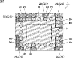
- FIG. 3 is a top view schematically showing an example of an embodiment of a circuit board.
- FIG. 4 is a top view schematically showing another example of the embodiment of the circuit board.
- FIG. 5 is a perspective view schematically showing a module in which electronic components are mounted on a circuit board and resin-molded.
- circuit board of the present invention will be described.
- the present invention is not limited to the following configuration, and can be appropriately modified and applied without changing the gist of the present invention. It should be noted that a combination of two or more of the individual desirable configurations described below is also the present invention.
- FIG. 1 is a top view schematically showing an electrode pad, a protruding electrode, and a coating layer formed on the surface of a substrate
- FIG. 2 is a cross-sectional view taken along the line AA of FIG.
- the circuit board of the present invention includes a substrate, an electrode pad formed on the surface of the substrate, a protruding electrode formed on the electrode pad, and a coating layer. 1 and 2 show two different modes on the left side and the right side as protruding electrodes formed on the electrode pads provided on the surface of the substrate 10.
- FIGS. 1 and 2 show an embodiment in which the protruding electrode 25 is formed on the electrode pad 20.
- the electrode pad 20 is an electrode pad whose top-viewed shape is larger than that of the protruding electrode 25.
- Two protruding electrodes 25 are provided on the electrode pad 20. Since the electrode pad 20 is an electrode pad larger than the protruding electrode 25, there is a portion on the surface of the substrate 10 where the electrode pad 20 is spread without being hidden by the protruding electrode 25.
- a coating layer is provided on at least a part of the outer periphery of the electrode pad on which the protruding electrode is formed.
- 1 and 2 show a coating layer 40 that covers at least a part of the outer periphery of the electrode pad 20. Further, since the electrode pad 20 is hidden by the coating layer 40, the outer circumference of the electrode pad 20 is shown by a dotted line. The covering layer 40 is provided to the outside of the dotted line.
- the outer periphery of the electrode pad may be peeled off when an impact is applied to the circuit board.
- a coating layer By covering the outer periphery of the electrode pad with a coating layer, it is possible to prevent peeling of the outer periphery of the electrode pad.
- the electrode pad provided with the coating layer is an electrode pad having a relatively large area, but when the portion where the electrode pad spreads without being hidden by the protruding electrode is large to some extent, the outer periphery of the electrode pad is likely to be peeled off due to an impact. .. From this point of view, when the circuit board is viewed from above, if the maximum length from the protruding electrode to the outer periphery of the electrode pad before the coating layer is provided is 30 ⁇ m or more, the effect of providing the coating layer is more effectively exhibited. Therefore, it is preferable.
- the coating layer 40 does not cover all of the electrode pads 20 exposed on the surface of the substrate 10, and the electrode pads 20 are exposed around the protruding electrodes 25. .. This reflects that in the process of manufacturing the circuit board, it is preferable in the process to provide the protruding electrode after forming the coating layer that covers the electrode pad, so that such a positional relationship is often obtained.
- the electrode pad 30 has the same shape as the protruding electrode 35 when viewed from above, and one protruding electrode 35 is provided on the electrode pad 30. Since the electrode pad 30 and the protruding electrode 25 have the same shape when viewed from above, the electrode pad 30 is hidden by the protruding electrode 35 on the surface of the substrate 10, and there is no portion where the electrode pad 30 is exposed. Therefore, there is no problem that the outer periphery of the electrode pad 30 is peeled off, and it is not necessary to provide a coating layer.
- the ground electrode pad connected to the ground is often a large electrode pad as shown on the left side of FIGS. 1 and 2. Further, as shown on the left side of FIGS. 1 and 2, a plurality of protruding electrodes are often formed on the ground electrode pad. That is, the electrode pad to which the coating layer is provided is preferably a ground electrode pad.
- the signal electrode pad serving as the signal terminal is often an electrode pad having the same area as the protruding electrode as shown on the right side of FIGS. 1 and 2. That is, it is often not necessary to provide a coating layer on the signal electrode pad.
- the substrate constituting the circuit board of the present invention is preferably a ceramic substrate.
- a low temperature sintered ceramic substrate (LTCC substrate) can be preferably used.
- the low-temperature sintered ceramic material is a ceramic material that can be sintered at a temperature of 1000 ° C. or lower and can be simultaneously fired with Au, Ag, Cu, etc. having a small specific resistance.
- Specific examples of the low-temperature sintered ceramic material include ZnO-MgO-Al 2 , a glass composite low-temperature sintered ceramic material obtained by mixing borosilicate-based glass with ceramic powders such as alumina, zirconia, magnesia, and forsterite.
- a resin substrate can be used in addition to the ceramic substrate.
- the resin substrate include a paper phenol substrate, a glass epoxy substrate, a BT (bismaleimide-triazine resin) substrate, a polyimide resin substrate and the like.
- the electrode pad one having a pattern formed by a method such as screen printing using a conductive paste or photolithography can be used.
- the conductive paste includes, for example, a conductive metal powder, a binder, a plasticizer, and the like.
- a co-based material (ceramic powder) for adjusting the shrinkage rate may be added to the conductive paste.
- the conductive metal material contained in the conductive paste include a metal containing at least one of Ag, Ag-Pt alloy, Ag-Pd alloy, Cu, Ni, Pt, Pd, W, Mo and Au as a main component. Etc. can be used.
- the thickness of the electrode pad is preferably, for example, 20 ⁇ m or more and 30 ⁇ m or less.
- a ceramic coating layer containing a ceramic material or a solder resist layer can be used as the coating layer constituting the circuit board of the present invention.
- the substrate is a ceramic substrate, it is preferable that the ceramic material contained in the ceramic coating layer is co-sintered with the ceramic material constituting the ceramic substrate.
- the coating layer is a ceramic coating layer
- the substrate is also a ceramic substrate.
- both the coating layer and the substrate are made of a ceramic material, the adhesiveness between the substrate and the coating layer is good, and the coefficient of thermal expansion is close to each other, so that peeling is unlikely to occur between the substrate and the coating layer.
- the ceramic material constituting the coating layer and the ceramic material constituting the ceramic substrate are the same ceramic material.
- a ceramic coating layer containing the above-mentioned low-temperature sintered ceramic material can be used. Further, a ceramic coating layer was formed by dispersing and kneading the mixed raw material powder obtained by adding and mixing an appropriate amount of alumina (Al 2 O 3 ) powder to the above low-temperature sintered ceramic material in an organic vehicle. The ceramic coating layer obtained by applying the ceramic paste for use and drying it can be used.
- the ceramic coating layer contains the low-temperature sintered ceramic material and further alumina, the coefficient of thermal expansion of the surface of the ceramic substrate made of the low-temperature sintered ceramic material can be matched with the coefficient of thermal expansion of the ceramic coating layer.
- the thermal expansion coefficient of the ceramic substrate and the ceramic coating layer can be more matched by containing alumina in the ceramic coating layer. can.
- the content of alumina added to the low-temperature sintered ceramic material is 2% by weight based on the total amount of the low-temperature sintered ceramic material and alumina. As mentioned above, it is preferably 15% by weight or less.
- a ceramic coating layer a ceramic for forming a ceramic coating layer obtained by dispersing and kneading a mixed raw material powder obtained by adding and mixing an appropriate amount of glass powder to the above-mentioned low-temperature sintered ceramic material in an organic vehicle.
- a ceramic coating layer obtained by applying a paste and drying it can also be used. By including the low temperature sintered ceramic material and further glass in the ceramic coating layer, cracking of the ceramic coating layer can be prevented. In addition, the plating resistance of the ceramic coating layer can be improved.
- the content of SiO 2 in the ceramic material in the ceramic coating layer is 5% by weight or more and 15% by weight as compared with the ceramic material constituting the ceramic substrate. It is preferable that the content is as high as% or less and the BaO content is as low as 5% by weight or more and 15% by weight or less.
- the ceramic material contained in the ceramic coating layer may have the same composition as the low-temperature sintered ceramic material constituting the low-temperature sintered ceramic substrate. Further, the ceramic material contained in the ceramic coating layer may include a low-temperature sintered ceramic material constituting the low-temperature sintered ceramic substrate, and further, alumina and glass.
- a solder resist layer made of a material used as a solder resist can also be used.
- the substrate is preferably a resin substrate.
- the substrate may be a ceramic substrate and the coating layer may be a solder resist layer, or the substrate may be a low-temperature sintered ceramic substrate and the coating layer may be a solder resist layer.
- the thickness of the coating layer is preferably, for example, 20 ⁇ m or more and 30 ⁇ m or less.
- the amount of overlap between the coating layer and the electrode pad on the outer periphery of the electrode pad is preferably 30 ⁇ m or more and 200 ⁇ m or less.
- the amount of alumina powder added is adjusted when preparing the ceramic paste for forming the ceramic coating layer.
- the thermal expansion coefficient of the ceramic coating layer can be adjusted. As a result, when the coefficient of thermal expansion of the substrate is ⁇ 1 , the coefficient of thermal expansion of the electrode pad is ⁇ 2 , and the coefficient of thermal expansion of the ceramic coating layer is ⁇ 3 , the relationship is ⁇ 3 ⁇ 1 ⁇ 2 . preferable.
- the coefficient of thermal expansion of the substrate is ⁇ 1 : 10 ppm / ° C
- the coefficient of thermal expansion of the electrode pad is ⁇ 2 : 16 ppm / ° C
- the coefficient of thermal expansion of the ceramic coating layer is ⁇ 3 : 9 ppm / ° C.
- the protruding electrode constituting the circuit board of the present invention is not particularly limited, and an electrode made of a conductive material that can be electrically connected to the electrode pad can be used.
- the shape of the protruding electrode is preferably cylindrical, having a diameter of 70 ⁇ m or more and 600 ⁇ m or less, and a height of 20 ⁇ m or more and 500 ⁇ m or less. Further, it is preferable that the aspect ratio (height / diameter) is 7 or more and 25 or less.
- the protruding electrode formed on the ground electrode pad and the protruding electrode formed on the signal electrode pad may have the same shape or different shapes.
- FIG. 3 is a top view schematically showing an example of an embodiment of a circuit board.
- the circuit board 1 shown in FIG. 3 has a region for mounting electronic components (region B surrounded by a dotted line in FIG. 3) in the central portion of the substrate 10, and electrode pads and protruding electrodes are provided around the region. It is formed.
- a land (not shown) for mounting an electronic component is provided in the area for mounting the electronic component.
- Examples of electronic components mounted on the board include ICs, filters, capacitors, inductors and the like. It is preferable that the height of the electronic component to be mounted is lower than the height of the protruding electrode.
- the substrate 10 is provided with an electrode pad 20 which is a ground electrode pad and an electrode pad 30 which is a signal electrode pad.
- the electrode pad 20 which is a ground electrode pad is provided with a protrusion electrode 25, and since the top view shape of the electrode pad 20 is larger than that of the protrusion electrode 25, the portion where the electrode pad 20 is exposed without being hidden by the protrusion electrode 25. Exists. By enlarging the ground electrode pad, the strength of the ground electrode pad can be improved, and the ground can be strengthened by connecting to the shield electrode on the outer peripheral portion.
- the coating layer 40 is provided between the outer periphery of the circuit board and the projection electrodes when the circuit board is viewed from above.
- the coating layer 40 is provided on the outside of the protrusion electrode 25. Since the electrode pad is easily peeled off by an impact on the outer peripheral side of the circuit board, providing a coating layer at this portion is effective in preventing the electrode pad from peeling off.
- the coating layer may include the outer periphery of the circuit board. Further, although the electronic component is mounted in the central portion of the substrate, if the ground electrode pad is provided on the central portion side of the substrate, the distance from the land electrode for mounting the component becomes small and there is a possibility of interference. Therefore, the electrode pad is enlarged on the outer peripheral portion of the substrate, and the coating layer is provided there.
- the coating layer 40 is provided on an electrode pad provided with a protruding electrode arranged at a corner when the circuit board is viewed from above.
- the four projection electrodes indicated by reference numeral 25a are the projection electrodes arranged at the four corners when the circuit board is viewed from above. It is in the corners of the circuit board that the electrode pads are particularly prone to peeling due to impact. Therefore, providing a coating layer at this portion is particularly effective in preventing the electrode pad from peeling off.
- a plurality of protruding electrodes 25 are formed on one electrode pad 20.
- the electrode pad 20 is a ground electrode pad, if a plurality of protruding electrodes are formed on one ground electrode pad, even if one protruding electrode is disconnected, the remaining protruding electrodes secure the connection. This is because it is preferable because it can be used.
- one protruding electrode 25 may be formed for one electrode pad 20.
- the electrode pad 30, which is a signal electrode pad, is provided with a protrusion electrode 35.
- the electrode pad 30 has the same shape as the protruding electrode 35 when viewed from above, and one protruding electrode 35 is provided on the electrode pad 30.
- the electrode pad 30 is not provided with a coating layer.
- FIG. 3 shows an embodiment in which a region for mounting an electronic component is present in the central portion of the substrate 10, and an electrode pad and a protruding electrode are formed around the region.
- the position where the electrode pad and the protruding electrode are provided is not particularly limited, and the position where the electrode pad and the protruding electrode are provided may be the central portion of the substrate.
- FIG. 4 is a top view schematically showing another example of the embodiment of the circuit board.
- the circuit board 2 shown in FIG. 4 also has a region for mounting electronic components (region C surrounded by a dotted line in FIG. 4) in the central portion of the substrate 10, and electrode pads and protruding electrodes are provided around the region. It is formed.
- a land (not shown) for mounting an electronic component is provided in the area for mounting the electronic component.
- the electrode pad 20 which is a ground electrode pad is provided inside the circuit board 2 with respect to the protrusion electrode 25.
- the coating layer 40 is provided inside the circuit board 2 with respect to the protrusion electrode 25.
- the total area of the electrode pads exposed on the front and back surfaces of the circuit board is about the same from the viewpoint of preventing the board from warping.
- the circuit board may be warped if the electrode pad becomes large. Therefore, it is possible to prevent the substrate from warping by providing a coating layer on the surface of the electrode pad provided inside the protruding electrode to reduce the total area of the electrode pad exposed on the surface of the substrate. can.
- the outer periphery of the electrode pad is exposed inside the circuit board without being covered by the coating layer, but unlike the outer peripheral side of the circuit board, the electrode is exposed in this region. Since the problem that the outer periphery of the pad is peeled off is unlikely to occur, there is no problem that the outer periphery of the electrode pad is exposed in this region.
- the coating layer 40 is provided between the plurality of projection electrodes 25 when the circuit board 2 is viewed from above.
- the region where the coating layer 40 is provided between the protrusion electrodes 25 is shown as a region E surrounded by a dotted line.
- the shape of the electrode pad 20 may be asymmetrical with respect to the protruding electrode 25b.
- the top view of the protruding electrode 25b shown in FIG. 4 is circular, whereas the electrode pad 20 has a notched shape inside the circuit board 2.
- a coating layer 40 is provided on the outer periphery of the electrode pad 20 on the outer peripheral side of the circuit board 2 with respect to the protruding electrode 25b.
- the module of the present invention includes the circuit board of the present invention, an electronic component mounted on the circuit board, and a mold resin for sealing the circuit board and the periphery of the electronic component, and the protruding electrode is the mold. It is exposed from the upper surface of the resin.
- FIG. 5 is a perspective view schematically showing a module in which electronic components are mounted on a circuit board and resin-molded.
- the electronic component 50 is mounted on the central portion of the circuit board 1 shown in FIG. 3, and is sealed with the mold resin 60.
- the protrusion electrode 25 and the upper surface of the protrusion electrode 35 are exposed on the upper surface of the mold resin 60 so that the protrusion electrode 25 and the protrusion electrode 35 of the circuit board 1 can be electrically connected to the outside on the upper surface of the mold resin 60. It has become.
- the heights of the protrusion electrode 25 and the protrusion electrode 35 are designed to be higher than the height of the electronic component 50.
- the electronic component 50 include at least one selected from the group consisting of ICs, filters, capacitors and inductors.
Landscapes
- Engineering & Computer Science (AREA)
- Microelectronics & Electronic Packaging (AREA)
- Chemical & Material Sciences (AREA)
- Ceramic Engineering (AREA)
- Inorganic Chemistry (AREA)
- Manufacturing & Machinery (AREA)
- Non-Metallic Protective Coatings For Printed Circuits (AREA)
- Electric Connection Of Electric Components To Printed Circuits (AREA)
Abstract
基板10と、上記基板10の表面に形成された電極パッド20と、上記電極パッド20上に形成された突起電極25と、を備え、上記突起電極25が形成された電極パッド20は、その上面視形状が上記突起電極25よりも大きく、上記突起電極25が形成された電極パッド20の外周の少なくとも一部に被覆層40が設けられていることを特徴とする回路基板1。
Description
本発明は、回路基板及びモジュールに関する。
回路基板として、基板に電子部品を実装し、基板の電子部品を実装した部位の周囲に突起電極を備えるものがある。
特許文献1では、電極パッド上に突起電極が形成されている。
特許文献1では、電極パッド上に突起電極が形成されている。
特許文献1に記載されているように、比較的面積が大きい電極パッド上に突起電極が形成されていると、回路基板に熱衝撃や落下衝撃といった衝撃が加わった際に電極パッドの外周が剥離することがあった。
とくに、回路基板を上面視した際に、電極パッドが回路基板の隅に位置する場合に衝撃による剥離が生じやすくなっていた。
とくに、回路基板を上面視した際に、電極パッドが回路基板の隅に位置する場合に衝撃による剥離が生じやすくなっていた。
本発明は上記の問題を解決するためになされたものであり、突起電極が形成された電極パッドが衝撃により剥離しにくい構成を有する回路基板、及び、上記回路基板を備えるモジュールを提供することを目的とする。
本発明の回路基板は、基板と、上記基板の表面に形成された電極パッドと、上記電極パッド上に形成された突起電極と、を備え、上記突起電極が形成された電極パッドは、その上面視形状が上記突起電極よりも大きく、上記突起電極が形成された電極パッドの外周の少なくとも一部に被覆層が設けられていることを特徴とする。
本発明のモジュールは、本発明の回路基板と、上記回路基板に実装された電子部品と、上記回路基板及び上記電子部品の周囲を封止するモールド樹脂と、を備え、上記突起電極が上記モールド樹脂の上面から露出してなることを特徴とする。
本発明によれば、突起電極が形成された電極パッドが衝撃により剥離しにくい構成を有する回路基板、及び、上記回路基板を備えるモジュールを提供することができる。
以下、本発明の回路基板について説明する。
しかしながら、本発明は、以下の構成に限定されるものではなく、本発明の要旨を変更しない範囲において適宜変更して適用することができる。なお、以下において記載する個々の望ましい構成を2つ以上組み合わせたものもまた本発明である。
しかしながら、本発明は、以下の構成に限定されるものではなく、本発明の要旨を変更しない範囲において適宜変更して適用することができる。なお、以下において記載する個々の望ましい構成を2つ以上組み合わせたものもまた本発明である。
図1は、基板の表面に形成された電極パッド、突起電極及び被覆層を模式的に示す上面図であり、図2は、図1のA-A線断面図である。
本発明の回路基板は、基板と、上記基板の表面に形成された電極パッドと、上記電極パッド上に形成された突起電極と、被覆層とを備える。
図1及び図2には、基板10の表面に設けられた電極パッド上に形成された突起電極として左側及び右側に異なる2種類の態様を合わせて示している。
本発明の回路基板は、基板と、上記基板の表面に形成された電極パッドと、上記電極パッド上に形成された突起電極と、被覆層とを備える。
図1及び図2には、基板10の表面に設けられた電極パッド上に形成された突起電極として左側及び右側に異なる2種類の態様を合わせて示している。
図1及び図2の左側には、電極パッド20の上に突起電極25が形成された態様を示している。電極パッド20は、その上面視した形状が突起電極25よりも大きい電極パッドである。そして、電極パッド20の上には突起電極25が2つ設けられている。電極パッド20は突起電極25よりも大きい電極パッドであるので、電極パッド20が基板10の表面で突起電極25に隠れることなく広がっている部位が存在する。
本発明の回路基板では、突起電極が形成された電極パッドの外周の少なくとも一部に被覆層が設けられる。
図1及び図2には、電極パッド20の外周の少なくとも一部を被覆する被覆層40を示している。また、電極パッド20が被覆層40に隠れるので、電極パッド20の外周を点線で示している。この点線よりも外側にまで被覆層40が設けられている。
図1及び図2には、電極パッド20の外周の少なくとも一部を被覆する被覆層40を示している。また、電極パッド20が被覆層40に隠れるので、電極パッド20の外周を点線で示している。この点線よりも外側にまで被覆層40が設けられている。
上述したように、比較的面積が大きい電極パッド上に突起電極が形成されていると、回路基板に衝撃が加わった際に電極パッドの外周が剥離することがある。電極パッドの外周を被覆層で被覆することにより、電極パッドの外周の剥離を防止することができる。
被覆層を設ける電極パッドは、比較的面積が大きい電極パッドであるが、電極パッドが突起電極に隠れることなく広がっている部位がある程度大きい場合に、衝撃による電極パッドの外周の剥離が生じやすくなる。その観点から、回路基板を上面視した際に、被覆層を設ける前での突起電極から電極パッドの外周までの最長長さが30μm以上であると、被覆層を設ける効果がより有効に発揮されるため好ましい。
また、図1及び図2に示す態様では、被覆層40は基板10の表面に露出する電極パッド20の全てを被覆するわけではなく、突起電極25の周囲においては電極パッド20が露出している。これは、回路基板の製造過程において、電極パッドを被覆する被覆層を形成した後に突起電極を設けることが工程上好ましいため、このような位置関係になることが多いことを反映している。
図1及び図2の右側には、電極パッド30の上に突起電極35が形成された態様を示している。電極パッド30は、その上面視した形状が突起電極35と同じ電極パッドであり、電極パッド30の上には突起電極35が1つ設けられている。
電極パッド30と突起電極25はその上面視した形状が同じであるので、電極パッド30は基板10の表面で突起電極35に隠れており、電極パッド30が露出した部位は存在しない。そのため、このような電極パッド30には外周が剥離するという問題は生じず、被覆層を設ける必要もない。
電極パッド30と突起電極25はその上面視した形状が同じであるので、電極パッド30は基板10の表面で突起電極35に隠れており、電極パッド30が露出した部位は存在しない。そのため、このような電極パッド30には外周が剥離するという問題は生じず、被覆層を設ける必要もない。
回路基板において、グランドに接続されるグランド電極パッドは、図1及び図2の左側に示すような大きい電極パッドとなることが多い。また、グランド電極パッドには、図1及び図2の左側に示すように、複数の突起電極を形成することが多い。
すなわち、被覆層を設ける対象となる電極パッドは、グランド電極パッドであることが好ましい。
すなわち、被覆層を設ける対象となる電極パッドは、グランド電極パッドであることが好ましい。
また、回路基板において、信号端子となる信号電極パッドは、図1及び図2の右側に示すような、突起電極と同じ面積の電極パッドとなることが多い。すなわち、信号電極パッドには被覆層を設ける必要がないことが多い。
本発明の回路基板を構成する基板は、セラミック基板であることが好ましい。
セラミック基板としては、低温焼結セラミック基板(LTCC基板)を好ましく用いることができる。
低温焼結セラミック材料とは、1000℃以下の温度で焼結可能であって、比抵抗の小さなAu、Ag、Cu等と同時焼成が可能なセラミック材料である。低温焼結セラミック材料としては、具体的には、アルミナ、ジルコニア、マグネシア、フォルステライト等のセラミック粉末にホウ珪酸系ガラスを混合してなるガラス複合系低温焼結セラミック材料、ZnO-MgO-Al2O3-SiO2系の結晶化ガラスを用いた結晶化ガラス系低温焼結セラミック材料、BaO-Al2O3-SiO2系セラミック粉末やAl2O3-CaO-SiO2-MgO-B2O3系セラミック粉末等を用いた非ガラス系低温焼結セラミック材料等が挙げられる。
セラミック基板としては、低温焼結セラミック基板(LTCC基板)を好ましく用いることができる。
低温焼結セラミック材料とは、1000℃以下の温度で焼結可能であって、比抵抗の小さなAu、Ag、Cu等と同時焼成が可能なセラミック材料である。低温焼結セラミック材料としては、具体的には、アルミナ、ジルコニア、マグネシア、フォルステライト等のセラミック粉末にホウ珪酸系ガラスを混合してなるガラス複合系低温焼結セラミック材料、ZnO-MgO-Al2O3-SiO2系の結晶化ガラスを用いた結晶化ガラス系低温焼結セラミック材料、BaO-Al2O3-SiO2系セラミック粉末やAl2O3-CaO-SiO2-MgO-B2O3系セラミック粉末等を用いた非ガラス系低温焼結セラミック材料等が挙げられる。
また、本発明の回路基板を構成する基板として、セラミック基板の他には樹脂基板を使用することができる。樹脂基板としては、紙フェノール基板、ガラスエポキシ基板、BT(ビスマレイミド-トリアジン樹脂)基板、ポリイミド樹脂基板等が挙げられる。
電極パッドとしては、導電性ペーストを用いたスクリーン印刷又はフォトリソグラフィ等の手法によりパターン形成されたものが使用できる。
導電性ペーストには、例えば、導電性金属粉末、バインダー及び可塑剤等が含まれる。導電性ペーストには、収縮率調整用の共素地(セラミック粉末)が添加されていてもよい。導電性ペーストに含まれる導電性金属材料としては、例えば、Ag、Ag-Pt合金、Ag-Pd合金、Cu、Ni、Pt、Pd、W、Mo及びAuの少なくとも1種を主成分とする金属等を用いることができる。これらの導電性金属材料のうち、Ag、Ag-Pt合金、Ag-Pd合金及びCuは、比抵抗が小さいため、特に高周波向けの導体パターンにおいてより好ましく用いることができる。
電極パッドの厚みは、例えば20μm以上30μm以下とすることが好ましい。
導電性ペーストには、例えば、導電性金属粉末、バインダー及び可塑剤等が含まれる。導電性ペーストには、収縮率調整用の共素地(セラミック粉末)が添加されていてもよい。導電性ペーストに含まれる導電性金属材料としては、例えば、Ag、Ag-Pt合金、Ag-Pd合金、Cu、Ni、Pt、Pd、W、Mo及びAuの少なくとも1種を主成分とする金属等を用いることができる。これらの導電性金属材料のうち、Ag、Ag-Pt合金、Ag-Pd合金及びCuは、比抵抗が小さいため、特に高周波向けの導体パターンにおいてより好ましく用いることができる。
電極パッドの厚みは、例えば20μm以上30μm以下とすることが好ましい。
本発明の回路基板を構成する被覆層としては、セラミック材料を含むセラミック被覆層、又はソルダーレジスト層を使用することができる。
基板がセラミック基板である場合は、セラミック被覆層に含まれるセラミック材料がセラミック基板を構成するセラミック材料と共焼結していることが好ましい。
基板がセラミック基板である場合は、セラミック被覆層に含まれるセラミック材料がセラミック基板を構成するセラミック材料と共焼結していることが好ましい。
被覆層がセラミック被覆層である場合、基板もセラミック基板であることが好ましい。被覆層と基板が共にセラミック材料であると、基板と被覆層の接着性が良く、また、熱膨張係数も近くなるので基板と被覆層の間に剥離が生じにくい。
また、被覆層を構成するセラミック材料とセラミック基板を構成するセラミック材料が同じセラミック材料であることが好ましい。
また、被覆層を構成するセラミック材料とセラミック基板を構成するセラミック材料が同じセラミック材料であることが好ましい。
セラミック被覆層としては、上記の低温焼結セラミック材料を含むセラミック被覆層を用いることができる。また、上記の低温焼結セラミック材料にアルミナ(Al2O3)粉末を適量添加、混合することにより得た混合原料粉末を、有機ビヒクル中に分散、混錬することにより得たセラミック被覆層形成用のセラミックペーストを塗布し、乾燥することで得られるセラミック被覆層を使用することができる。
セラミック被覆層が、低温焼結セラミック材料とさらにアルミナを含むことによって、低温焼結セラミック材料からなるセラミック基板の表面の熱膨張係数とセラミック被覆層の熱膨張係数を整合させることができる。とくに、セラミック基板の表面に、アルミナを用いた拘束層に由来するアルミナ成分が存在する場合、セラミック被覆層がアルミナを含むことによって、セラミック基板とセラミック被覆層の熱膨張係数をより整合させることができる。
セラミック被覆層が、低温焼結セラミック材料とさらにアルミナを含むことによって、低温焼結セラミック材料からなるセラミック基板の表面の熱膨張係数とセラミック被覆層の熱膨張係数を整合させることができる。とくに、セラミック基板の表面に、アルミナを用いた拘束層に由来するアルミナ成分が存在する場合、セラミック被覆層がアルミナを含むことによって、セラミック基板とセラミック被覆層の熱膨張係数をより整合させることができる。
また、セラミック被覆層が、低温焼結セラミック材料とさらにアルミナを含む場合、低温焼結セラミック材料に添加されるアルミナの含有量は、低温焼結セラミック材料とアルミナの合計量に対して2重量%以上、15重量%以下であることが好ましい。
セラミック被覆層として、上記の低温焼結セラミック材料にガラス粉末を適量添加、混合することにより得た混合原料粉末を、有機ビヒクル中に分散、混錬することにより得たセラミック被覆層形成用のセラミックペーストを塗布し、乾燥することで得られるセラミック被覆層を使用することもできる。
セラミック被覆層が、低温焼結セラミック材料とさらにガラスを含むことによって、セラミック被覆層の割れを防止することができる。また、セラミック被覆層の耐めっき性を向上させることができる。
セラミック被覆層が、低温焼結セラミック材料とさらにガラスを含むことによって、セラミック被覆層の割れを防止することができる。また、セラミック被覆層の耐めっき性を向上させることができる。
セラミック被覆層が、低温焼結セラミック材料とさらにガラスを含む場合、セラミック基板を構成するセラミック材料と比較して、セラミック被覆層におけるセラミック材料中のSiO2の含有率が5重量%以上、15重量%以下高く、BaOの含有率が5重量%以上、15重量%以下低くなることが好ましい。
また、セラミック被覆層に含まれるセラミック材料は、低温焼結セラミック基板を構成する低温焼結セラミック材料と同一組成であってもよい。
また、セラミック被覆層に含まれるセラミック材料は、低温焼結セラミック基板を構成する低温焼結セラミック材料と、さらにアルミナ及びガラスを含んでいてもよい。
また、セラミック被覆層に含まれるセラミック材料は、低温焼結セラミック基板を構成する低温焼結セラミック材料と、さらにアルミナ及びガラスを含んでいてもよい。
本発明の回路基板を構成する被覆層としては、ソルダーレジストとして使用される材料からなるソルダーレジスト層を使用することもできる。
被覆層がソルダーレジスト層である場合、基板は樹脂基板であることが好ましい。また、基板がセラミック基板であって被覆層がソルダーレジスト層であってもよく、基板が低温焼結セラミック基板であって被覆層がソルダーレジスト層であってもよい。
被覆層がソルダーレジスト層である場合、基板は樹脂基板であることが好ましい。また、基板がセラミック基板であって被覆層がソルダーレジスト層であってもよく、基板が低温焼結セラミック基板であって被覆層がソルダーレジスト層であってもよい。
被覆層の厚みは、例えば20μm以上30μm以下とすることが好ましい。
また、電極パッドの外周における被覆層と電極パッドの重なり量は、30μm以上200μm以下であることが好ましい。
被覆層の熱膨張係数を基板の熱膨張係数に近づけることにより、被覆層を設けることによる電極パッドの剥離防止効果を高めることができる。
また、電極パッドの外周における被覆層と電極パッドの重なり量は、30μm以上200μm以下であることが好ましい。
被覆層の熱膨張係数を基板の熱膨張係数に近づけることにより、被覆層を設けることによる電極パッドの剥離防止効果を高めることができる。
セラミック被覆層が、低温焼結セラミック基板を構成する低温焼結セラミック材料とさらにアルミナを含む場合に、セラミック被覆層形成用のセラミックペーストを作製する際、アルミナ粉末の添加量を調整することにより、セラミック被覆層の熱膨張係数を調整することができる。その結果、基板の熱膨張係数をα1、電極パッドの熱膨張係数をα2、セラミック被覆層の熱膨張係数をα3としたとき、α3<α1<α2の関係とすることが好ましい。例えば、基板の熱膨張係数α1:10ppm/℃、電極パッドの熱膨張係数α2:16ppm/℃、セラミック被覆層の熱膨張係数α3:9ppm/℃とすることが好ましい。
本発明の回路基板を構成する突起電極は、特に限定されるものではなく、電極パッドと電気的に接続可能な導電材料からなる電極を使用することができる。
突起電極の形状としては、円柱状であり、その直径が70μm以上、600μm以下、その高さが20μm以上、500μm以下であるものが好ましい。
また、そのアスペクト比(高さ/直径)が7以上、25以下であるものが好ましい。
グランド電極パッド上に形成される突起電極と、信号電極パッド上に形成される突起電極は、同じ形状であっても異なる形状であってもよい。
突起電極の形状としては、円柱状であり、その直径が70μm以上、600μm以下、その高さが20μm以上、500μm以下であるものが好ましい。
また、そのアスペクト比(高さ/直径)が7以上、25以下であるものが好ましい。
グランド電極パッド上に形成される突起電極と、信号電極パッド上に形成される突起電極は、同じ形状であっても異なる形状であってもよい。
続いて、本発明の回路基板の好ましい実施形態について説明する。
図3は、回路基板の実施形態の一例を模式的に示す上面図である。
図3に示す回路基板1には、基板10の中央部に電子部品を実装するための領域(図3中、点線で囲む領域B)が存在し、当該領域の周囲に電極パッド及び突起電極が形成されている。電子部品を実装するための領域には、電子部品実装用のランド(図示しない)が設けられている。
図3は、回路基板の実施形態の一例を模式的に示す上面図である。
図3に示す回路基板1には、基板10の中央部に電子部品を実装するための領域(図3中、点線で囲む領域B)が存在し、当該領域の周囲に電極パッド及び突起電極が形成されている。電子部品を実装するための領域には、電子部品実装用のランド(図示しない)が設けられている。
基板に実装する電子部品としては、IC、フィルタ、コンデンサ、インダクタ等が挙げられる。
実装する電子部品の高さが突起電極の高さよりも低くなることが好ましい。
実装する電子部品の高さが突起電極の高さよりも低くなることが好ましい。
基板10には、グランド電極パッドである電極パッド20と、信号電極パッドである電極パッド30が設けられている。
グランド電極パッドである電極パッド20には突起電極25が設けられていて、電極パッド20はその上面視形状が突起電極25よりも大きいので、電極パッド20が突起電極25に隠れることなく露出した部位が存在する。
グランド電極パッドを大きくすることで、グランド電極パッドの強度を向上させ、外周部のシールド電極に接続させてグランドを強化することができる。
グランド電極パッドを大きくすることで、グランド電極パッドの強度を向上させ、外周部のシールド電極に接続させてグランドを強化することができる。
被覆層40は、回路基板を上面視した際の回路基板の外周と突起電極の間に設けられている。言い換えると、被覆層40は突起電極25の外側に設けられている。
衝撃によって電極パッドが剥離しやすいのは回路基板の外周側であるので、この部位に被覆層を設けることは、電極パッドの剥離防止により有効である。
被覆層は回路基板の外周を含んでいてもよい。
また、基板の中央部には電子部品が実装されるが、グランド電極パッドが基板中央部側に設けられると、部品実装用のランド電極との距離が小さくなり、干渉する可能性がある。そのため、基板の外周部で電極パッドを大きくして、そこに被覆層を設けるようにしている。
衝撃によって電極パッドが剥離しやすいのは回路基板の外周側であるので、この部位に被覆層を設けることは、電極パッドの剥離防止により有効である。
被覆層は回路基板の外周を含んでいてもよい。
また、基板の中央部には電子部品が実装されるが、グランド電極パッドが基板中央部側に設けられると、部品実装用のランド電極との距離が小さくなり、干渉する可能性がある。そのため、基板の外周部で電極パッドを大きくして、そこに被覆層を設けるようにしている。
また、被覆層40は、回路基板を上面視した際に隅に配置されている突起電極が設けられた電極パッドに対して設けられている。
図3において参照符号25aで示す4つの突起電極が回路基板を上面視した際に4隅に配置されている突起電極である。
衝撃によって電極パッドが特に剥離しやすいのは回路基板の隅である。そのため、この部位に被覆層を設けることは、電極パッドの剥離防止に特に有効である。
図3において参照符号25aで示す4つの突起電極が回路基板を上面視した際に4隅に配置されている突起電極である。
衝撃によって電極パッドが特に剥離しやすいのは回路基板の隅である。そのため、この部位に被覆層を設けることは、電極パッドの剥離防止に特に有効である。
1つの電極パッド20には複数の突起電極25が形成されていることが好ましい。電極パッド20がグランド電極パッドである場合、1つのグランド電極パッドに対して複数の突起電極が形成されていると、1つの突起電極の接続が外れたとしても残りの突起電極で接続を確保することができるので好ましいためである。
また、1つの電極パッド20に対して1つの突起電極25が形成されていてもよい。図3において参照符号25bで示す、図3の上下に1つずつ設けられた突起電極が、1つの電極パッドに対して1つ形成された突起電極である。
信号電極パッドである電極パッド30には突起電極35が設けられている。電極パッド30は、その上面視した形状が突起電極35と同じ電極パッドであり、電極パッド30の上には突起電極35が1つ設けられている。
電極パッド30には被覆層は設けられていない。
電極パッド30には被覆層は設けられていない。
なお、図3には基板10の中央部に電子部品を実装するための領域が存在し、当該領域の周囲に電極パッド及び突起電極が形成された態様を示している。しかしながら、本発明の回路基板の実施形態において電極パッド及び突起電極が設けられる位置は特に限定されるものではなく、電極パッド及び突起電極が設けられる位置が基板の中央部であってもよい。
図4は、回路基板の実施形態の別の一例を模式的に示す上面図である。
図4に示す回路基板2にも、基板10の中央部に電子部品を実装するための領域(図4中、点線で囲む領域C)が存在し、当該領域の周囲に電極パッド及び突起電極が形成されている。電子部品を実装するための領域には、電子部品実装用のランド(図示しない)が設けられている。
以下には、図3に示す実施形態の回路基板と異なる事項について説明する。
図4に示す回路基板2にも、基板10の中央部に電子部品を実装するための領域(図4中、点線で囲む領域C)が存在し、当該領域の周囲に電極パッド及び突起電極が形成されている。電子部品を実装するための領域には、電子部品実装用のランド(図示しない)が設けられている。
以下には、図3に示す実施形態の回路基板と異なる事項について説明する。
図4に示す回路基板2では、回路基板2を上面視した際に、グランド電極パッドである電極パッド20が突起電極25よりも回路基板2の内側に設けられている。そして、被覆層40が突起電極25よりも回路基板2の内側に設けられている。
回路基板において基板の表裏面に露出している電極パッドの総面積は、基板反りを防止する観点からは同程度であることが好ましい。しかし、突起電極の内側にまで電極パッドを設ける場合、電極パッドが大きくなると、回路基板に反りが生じることがある。そのため、突起電極の内側に設けた電極パッドの表面に対しても被覆層を設けて基板の表面に露出する電極パッドの総面積を小さくすることによって、基板に反りが生じることを防止することができる。
なお、図4で点線で囲む領域Dで示す部分では、回路基板の内側で電極パッドの外周が被覆層に覆われずに露出しているが、回路基板の外周側とは異なりこの領域では電極パッドの外周が剥離するという問題が生じにくいため、この領域において電極パッドの外周が露出していることは問題ない。
また、図4で示す回路基板2では、被覆層40は、回路基板2を上面視した際の複数の突起電極25の間に設けられている。
図4には、突起電極25の間で被覆層40が設けられている領域を点線で囲む領域Eとして示している。
突起電極の間で露出している電極パッドに対して被覆層を設けることにより、基板の表面に露出する電極パッドの総面積を小さくすることができる。そのため、基板に反りが生じることを防止することができる。
図4には、突起電極25の間で被覆層40が設けられている領域を点線で囲む領域Eとして示している。
突起電極の間で露出している電極パッドに対して被覆層を設けることにより、基板の表面に露出する電極パッドの総面積を小さくすることができる。そのため、基板に反りが生じることを防止することができる。
また、1つの電極パッド20に対して1つの突起電極25bが形成されている場合、突起電極25bに対して電極パッド20の形状が非対称であってもよい。
図4に示す突起電極25bの上面視形状は円形であるのに対し、電極パッド20は回路基板2の内側において切り欠かれた形状になっている。
突起電極25bよりも回路基板2の外周側において、電極パッド20の外周に被覆層40が設けられている。
図4に示す突起電極25bの上面視形状は円形であるのに対し、電極パッド20は回路基板2の内側において切り欠かれた形状になっている。
突起電極25bよりも回路基板2の外周側において、電極パッド20の外周に被覆層40が設けられている。
本発明のモジュールは、本発明の回路基板と、上記回路基板に実装された電子部品と、上記回路基板及び上記電子部品の周囲を封止するモールド樹脂と、を備え、上記突起電極が上記モールド樹脂の上面から露出してなる。
図5は、回路基板に電子部品を実装し、樹脂モールドしたモジュールを模式的に示す斜視図である。
図5に示すモジュール100では、図3に示す回路基板1の中央部に電子部品50が実装され、モールド樹脂60で封止された状態を示している。モールド樹脂60の上面には突起電極25及び突起電極35の上面が露出するようにして、モールド樹脂60の上面において回路基板1の突起電極25及び突起電極35と外部との電気的接続が取れるようになっている。
また、突起電極25及び突起電極35の高さは電子部品50の高さよりも高くなるように設計している。
電子部品50としては、IC、フィルタ、コンデンサ及びインダクタからなる群から選択された少なくとも1種が挙げられる。
図5に示すモジュール100では、図3に示す回路基板1の中央部に電子部品50が実装され、モールド樹脂60で封止された状態を示している。モールド樹脂60の上面には突起電極25及び突起電極35の上面が露出するようにして、モールド樹脂60の上面において回路基板1の突起電極25及び突起電極35と外部との電気的接続が取れるようになっている。
また、突起電極25及び突起電極35の高さは電子部品50の高さよりも高くなるように設計している。
電子部品50としては、IC、フィルタ、コンデンサ及びインダクタからなる群から選択された少なくとも1種が挙げられる。
このようにモールド樹脂で封止されたモジュールにおいては、モジュールに熱衝撃が加わった際に、モールド樹脂の熱膨張係数と基板の熱膨張係数の差により、電極パッドの外周に力が加わることがあったが、電極パッドの外周に被覆層を設けることによって、熱衝撃による電極パッドの剥離を防止することができる。
1、2 回路基板
10 基板
20 電極パッド(グランド電極パッド)
25 突起電極
25a 上面視で4隅に配置されている突起電極
25b 1つの電極パッドに対して1つ形成された突起電極
30 電極パッド(信号電極パッド)
35 突起電極
40 被覆層
50 電子部品
60 モールド樹脂
100 モジュール
10 基板
20 電極パッド(グランド電極パッド)
25 突起電極
25a 上面視で4隅に配置されている突起電極
25b 1つの電極パッドに対して1つ形成された突起電極
30 電極パッド(信号電極パッド)
35 突起電極
40 被覆層
50 電子部品
60 モールド樹脂
100 モジュール
Claims (15)
- 基板と、前記基板の表面に形成された電極パッドと、前記電極パッド上に形成された突起電極と、を備え、
前記突起電極が形成された電極パッドは、その上面視形状が前記突起電極よりも大きく、
前記突起電極が形成された電極パッドの外周の少なくとも一部に被覆層が設けられていることを特徴とする回路基板。 - 1つの前記電極パッド上に複数の前記突起電極が形成されている電極パッドを含む請求項1に記載の回路基板。
- 前記被覆層が設けられた前記電極パッドは、グランド電極パッドである請求項1又は2に記載の回路基板。
- 前記被覆層は、前記回路基板を上面視した際に隅に配置されている突起電極が設けられた電極パッドに対して設けられている請求項1~3のいずれかに記載の回路基板。
- 前記被覆層は、前記回路基板を上面視した際の前記回路基板の外周と前記突起電極の間に設けられている請求項1~4のいずれかに記載の回路基板。
- 前記被覆層は、前記回路基板を上面視した際の複数の前記突起電極の間に設けられている請求項1~5のいずれかに記載の回路基板。
- 前記被覆層は、前記回路基板を上面視した際の前記突起電極よりも前記回路基板の内側に設けられている請求項1~6のいずれかに記載の回路基板。
- 前記基板はセラミック基板である請求項1~7のいずれかに記載の回路基板。
- 前記セラミック基板は低温焼結セラミック基板である請求項8に記載の回路基板。
- 前記被覆層はセラミック被覆層である請求項1~9のいずれかに記載の回路基板。
- 前記被覆層はセラミック被覆層であり、かつ、前記セラミック基板は低温焼結セラミック基板であり、前記セラミック被覆層は、前記低温焼結セラミック基板を構成する低温焼結セラミック材料と、さらにアルミナを含む請求項1~7のいずれかに記載の回路基板。
- 前記被覆層はセラミック被覆層であり、かつ、前記セラミック基板は低温焼結セラミック基板であり、前記セラミック被覆層は、前記低温焼結セラミック基板を構成する低温焼結セラミック材料と、さらにガラスを含む請求項1~7のいずれかに記載の回路基板。
- 請求項1~12のいずれかに記載の回路基板と、
前記回路基板に実装された電子部品と、
前記回路基板及び前記電子部品の周囲を封止するモールド樹脂と、を備え、
前記突起電極が前記モールド樹脂の上面から露出してなることを特徴とするモジュール。 - 前記電子部品が、IC、フィルタ、コンデンサ及びインダクタからなる群から選択された少なくとも1種である請求項13に記載のモジュール。
- 前記突起電極の高さが前記電子部品の高さより高い請求項13又は14に記載のモジュール。
Priority Applications (2)
| Application Number | Priority Date | Filing Date | Title |
|---|---|---|---|
| CN202190000758.9U CN220123154U (zh) | 2020-09-25 | 2021-09-22 | 电路基板和模块 |
| US18/189,460 US12396094B2 (en) | 2020-09-25 | 2023-03-24 | Circuit substrate and module |
Applications Claiming Priority (2)
| Application Number | Priority Date | Filing Date | Title |
|---|---|---|---|
| JP2020-160822 | 2020-09-25 | ||
| JP2020160822 | 2020-09-25 |
Related Child Applications (1)
| Application Number | Title | Priority Date | Filing Date |
|---|---|---|---|
| US18/189,460 Continuation US12396094B2 (en) | 2020-09-25 | 2023-03-24 | Circuit substrate and module |
Publications (1)
| Publication Number | Publication Date |
|---|---|
| WO2022065373A1 true WO2022065373A1 (ja) | 2022-03-31 |
Family
ID=80846544
Family Applications (1)
| Application Number | Title | Priority Date | Filing Date |
|---|---|---|---|
| PCT/JP2021/034828 Ceased WO2022065373A1 (ja) | 2020-09-25 | 2021-09-22 | 回路基板及びモジュール |
Country Status (3)
| Country | Link |
|---|---|
| US (1) | US12396094B2 (ja) |
| CN (1) | CN220123154U (ja) |
| WO (1) | WO2022065373A1 (ja) |
Citations (4)
| Publication number | Priority date | Publication date | Assignee | Title |
|---|---|---|---|---|
| JP2004014616A (ja) * | 2002-06-04 | 2004-01-15 | Sumitomo Metal Electronics Devices Inc | セラミック回路基板用外部接続端子 |
| WO2007049458A1 (ja) * | 2005-10-26 | 2007-05-03 | Murata Manufacturing Co., Ltd. | 積層型電子部品、電子装置および積層型電子部品の製造方法 |
| WO2008004423A1 (en) * | 2006-06-15 | 2008-01-10 | Murata Manufacturing Co., Ltd. | Wiring board having columnar conductor and method for manufacturing the wiring board |
| JP2017152678A (ja) * | 2016-02-22 | 2017-08-31 | 京セラ株式会社 | 配線基板、電子装置および配線基板の製造方法 |
Family Cites Families (5)
| Publication number | Priority date | Publication date | Assignee | Title |
|---|---|---|---|---|
| JP4706929B2 (ja) | 2006-06-01 | 2011-06-22 | Tdk株式会社 | 複合配線基板及びその製造方法 |
| TWI443789B (zh) * | 2008-07-04 | 2014-07-01 | 欣興電子股份有限公司 | 嵌埋有半導體晶片之電路板及其製法 |
| US9508671B2 (en) * | 2015-04-20 | 2016-11-29 | Advanced Semiconductor Engineering, Inc. | Semiconductor device and semiconductor package |
| CN109156080B (zh) * | 2016-05-16 | 2021-10-08 | 株式会社村田制作所 | 陶瓷电子部件 |
| WO2020129808A1 (ja) * | 2018-12-21 | 2020-06-25 | 株式会社村田製作所 | 電子部品モジュールの製造方法及び電子部品モジュール |
-
2021
- 2021-09-22 WO PCT/JP2021/034828 patent/WO2022065373A1/ja not_active Ceased
- 2021-09-22 CN CN202190000758.9U patent/CN220123154U/zh active Active
-
2023
- 2023-03-24 US US18/189,460 patent/US12396094B2/en active Active
Patent Citations (4)
| Publication number | Priority date | Publication date | Assignee | Title |
|---|---|---|---|---|
| JP2004014616A (ja) * | 2002-06-04 | 2004-01-15 | Sumitomo Metal Electronics Devices Inc | セラミック回路基板用外部接続端子 |
| WO2007049458A1 (ja) * | 2005-10-26 | 2007-05-03 | Murata Manufacturing Co., Ltd. | 積層型電子部品、電子装置および積層型電子部品の製造方法 |
| WO2008004423A1 (en) * | 2006-06-15 | 2008-01-10 | Murata Manufacturing Co., Ltd. | Wiring board having columnar conductor and method for manufacturing the wiring board |
| JP2017152678A (ja) * | 2016-02-22 | 2017-08-31 | 京セラ株式会社 | 配線基板、電子装置および配線基板の製造方法 |
Also Published As
| Publication number | Publication date |
|---|---|
| CN220123154U (zh) | 2023-12-01 |
| US20230232531A1 (en) | 2023-07-20 |
| US12396094B2 (en) | 2025-08-19 |
Similar Documents
| Publication | Publication Date | Title |
|---|---|---|
| US6338893B1 (en) | Conductive paste and ceramic printed circuit substrate using the same | |
| JP2002198660A (ja) | 回路基板及びその製造方法 | |
| US20070274055A1 (en) | Surface Mountable Device | |
| US7009114B2 (en) | Wiring substrate, method of producing the same, and electronic device using the same | |
| JP2680443B2 (ja) | セラミック配線基板およびその製造方法 | |
| JP5582069B2 (ja) | セラミック多層基板 | |
| JP4000633B2 (ja) | 配線基板の製造方法 | |
| CN220123154U (zh) | 电路基板和模块 | |
| US20230113966A1 (en) | Electronic component and method for manufacturing electronic component | |
| CN100551208C (zh) | 陶瓷基板制造方法以及使用该陶瓷基板的电子元件模块 | |
| JP4077625B2 (ja) | 低温焼成磁器組成物および低温焼成磁器の製造方法 | |
| JPH11273997A (ja) | 電子部品及びその製造方法 | |
| JPH0795630B2 (ja) | 複合積層セラミック部品 | |
| JP2004165343A (ja) | 積層型セラミック電子部品およびその製造方法 | |
| JP2003078103A (ja) | 回路基板 | |
| JP2001284819A (ja) | 積層回路基板 | |
| JP2010232257A (ja) | 多層配線基板 | |
| JP3905991B2 (ja) | ガラスセラミック配線基板 | |
| JP3450119B2 (ja) | メタライズ組成物及びそれを用いた配線基板 | |
| JP2001308667A (ja) | Lcフィルタ | |
| JPH1098244A (ja) | 厚膜回路基板及びその製造方法 | |
| JP2604416B2 (ja) | 複合積層セラミック部品 | |
| JP3934910B2 (ja) | 回路基板 | |
| JP3935833B2 (ja) | 電子装置 | |
| WO2025121101A1 (ja) | 回路モジュール |
Legal Events
| Date | Code | Title | Description |
|---|---|---|---|
| 121 | Ep: the epo has been informed by wipo that ep was designated in this application |
Ref document number: 21872502 Country of ref document: EP Kind code of ref document: A1 |
|
| NENP | Non-entry into the national phase |
Ref country code: DE |
|
| 122 | Ep: pct application non-entry in european phase |
Ref document number: 21872502 Country of ref document: EP Kind code of ref document: A1 |
|
| NENP | Non-entry into the national phase |
Ref country code: JP |