WO2022050354A1 - 実装構造体、ledディスプレイ、及び実装方法 - Google Patents
実装構造体、ledディスプレイ、及び実装方法 Download PDFInfo
- Publication number
- WO2022050354A1 WO2022050354A1 PCT/JP2021/032305 JP2021032305W WO2022050354A1 WO 2022050354 A1 WO2022050354 A1 WO 2022050354A1 JP 2021032305 W JP2021032305 W JP 2021032305W WO 2022050354 A1 WO2022050354 A1 WO 2022050354A1
- Authority
- WO
- WIPO (PCT)
- Prior art keywords
- mold
- copper
- substrate
- mounting structure
- metal
- Prior art date
- Legal status (The legal status is an assumption and is not a legal conclusion. Google has not performed a legal analysis and makes no representation as to the accuracy of the status listed.)
- Ceased
Links
Images



Classifications
-
- H—ELECTRICITY
- H10—SEMICONDUCTOR DEVICES; ELECTRIC SOLID-STATE DEVICES NOT OTHERWISE PROVIDED FOR
- H10W—GENERIC PACKAGES, INTERCONNECTIONS, CONNECTORS OR OTHER CONSTRUCTIONAL DETAILS OF DEVICES COVERED BY CLASS H10
- H10W90/00—Package configurations
- H10W90/701—Package configurations characterised by the relative positions of pads or connectors relative to package parts
-
- H—ELECTRICITY
- H10—SEMICONDUCTOR DEVICES; ELECTRIC SOLID-STATE DEVICES NOT OTHERWISE PROVIDED FOR
- H10H—INORGANIC LIGHT-EMITTING SEMICONDUCTOR DEVICES HAVING POTENTIAL BARRIERS
- H10H20/00—Individual inorganic light-emitting semiconductor devices having potential barriers, e.g. light-emitting diodes [LED]
- H10H20/01—Manufacture or treatment
-
- H—ELECTRICITY
- H05—ELECTRIC TECHNIQUES NOT OTHERWISE PROVIDED FOR
- H05K—PRINTED CIRCUITS; CASINGS OR CONSTRUCTIONAL DETAILS OF ELECTRIC APPARATUS; MANUFACTURE OF ASSEMBLAGES OF ELECTRICAL COMPONENTS
- H05K1/00—Printed circuits
- H05K1/18—Printed circuits structurally associated with non-printed electric components
- H05K1/181—Printed circuits structurally associated with non-printed electric components associated with surface mounted components
-
- H—ELECTRICITY
- H05—ELECTRIC TECHNIQUES NOT OTHERWISE PROVIDED FOR
- H05K—PRINTED CIRCUITS; CASINGS OR CONSTRUCTIONAL DETAILS OF ELECTRIC APPARATUS; MANUFACTURE OF ASSEMBLAGES OF ELECTRICAL COMPONENTS
- H05K3/00—Apparatus or processes for manufacturing printed circuits
- H05K3/10—Apparatus or processes for manufacturing printed circuits in which conductive material is applied to the insulating support in such a manner as to form the desired conductive pattern
- H05K3/20—Apparatus or processes for manufacturing printed circuits in which conductive material is applied to the insulating support in such a manner as to form the desired conductive pattern by affixing prefabricated conductor pattern
-
- H—ELECTRICITY
- H05—ELECTRIC TECHNIQUES NOT OTHERWISE PROVIDED FOR
- H05K—PRINTED CIRCUITS; CASINGS OR CONSTRUCTIONAL DETAILS OF ELECTRIC APPARATUS; MANUFACTURE OF ASSEMBLAGES OF ELECTRICAL COMPONENTS
- H05K3/00—Apparatus or processes for manufacturing printed circuits
- H05K3/30—Assembling printed circuits with electric components, e.g. with resistors
- H05K3/32—Assembling printed circuits with electric components, e.g. with resistors electrically connecting electric components or wires to printed circuits
-
- H—ELECTRICITY
- H10—SEMICONDUCTOR DEVICES; ELECTRIC SOLID-STATE DEVICES NOT OTHERWISE PROVIDED FOR
- H10H—INORGANIC LIGHT-EMITTING SEMICONDUCTOR DEVICES HAVING POTENTIAL BARRIERS
- H10H20/00—Individual inorganic light-emitting semiconductor devices having potential barriers, e.g. light-emitting diodes [LED]
- H10H20/80—Constructional details
- H10H20/85—Packages
- H10H20/857—Interconnections, e.g. lead-frames, bond wires or solder balls
-
- H—ELECTRICITY
- H10—SEMICONDUCTOR DEVICES; ELECTRIC SOLID-STATE DEVICES NOT OTHERWISE PROVIDED FOR
- H10W—GENERIC PACKAGES, INTERCONNECTIONS, CONNECTORS OR OTHER CONSTRUCTIONAL DETAILS OF DEVICES COVERED BY CLASS H10
- H10W70/00—Package substrates; Interposers; Redistribution layers [RDL]
- H10W70/60—Insulating or insulated package substrates; Interposers; Redistribution layers
-
- H—ELECTRICITY
- H10—SEMICONDUCTOR DEVICES; ELECTRIC SOLID-STATE DEVICES NOT OTHERWISE PROVIDED FOR
- H10W—GENERIC PACKAGES, INTERCONNECTIONS, CONNECTORS OR OTHER CONSTRUCTIONAL DETAILS OF DEVICES COVERED BY CLASS H10
- H10W72/00—Interconnections or connectors in packages
- H10W72/01—Manufacture or treatment
- H10W72/012—Manufacture or treatment of bump connectors, dummy bumps or thermal bumps
- H10W72/01251—Changing the shapes of bumps
-
- H—ELECTRICITY
- H10—SEMICONDUCTOR DEVICES; ELECTRIC SOLID-STATE DEVICES NOT OTHERWISE PROVIDED FOR
- H10W—GENERIC PACKAGES, INTERCONNECTIONS, CONNECTORS OR OTHER CONSTRUCTIONAL DETAILS OF DEVICES COVERED BY CLASS H10
- H10W90/00—Package configurations
-
- B—PERFORMING OPERATIONS; TRANSPORTING
- B82—NANOTECHNOLOGY
- B82Y—SPECIFIC USES OR APPLICATIONS OF NANOSTRUCTURES; MEASUREMENT OR ANALYSIS OF NANOSTRUCTURES; MANUFACTURE OR TREATMENT OF NANOSTRUCTURES
- B82Y30/00—Nanotechnology for materials or surface science, e.g. nanocomposites
-
- H—ELECTRICITY
- H05—ELECTRIC TECHNIQUES NOT OTHERWISE PROVIDED FOR
- H05K—PRINTED CIRCUITS; CASINGS OR CONSTRUCTIONAL DETAILS OF ELECTRIC APPARATUS; MANUFACTURE OF ASSEMBLAGES OF ELECTRICAL COMPONENTS
- H05K1/00—Printed circuits
- H05K1/02—Details
- H05K1/09—Use of materials for the conductive, e.g. metallic pattern
- H05K1/092—Dispersed materials, e.g. conductive pastes or inks
- H05K1/097—Inks comprising nanoparticles and specially adapted for being sintered at low temperature
-
- H—ELECTRICITY
- H05—ELECTRIC TECHNIQUES NOT OTHERWISE PROVIDED FOR
- H05K—PRINTED CIRCUITS; CASINGS OR CONSTRUCTIONAL DETAILS OF ELECTRIC APPARATUS; MANUFACTURE OF ASSEMBLAGES OF ELECTRICAL COMPONENTS
- H05K2203/00—Indexing scheme relating to apparatus or processes for manufacturing printed circuits covered by H05K3/00
- H05K2203/10—Using electric, magnetic and electromagnetic fields; Using laser light
- H05K2203/107—Using laser light
-
- H—ELECTRICITY
- H05—ELECTRIC TECHNIQUES NOT OTHERWISE PROVIDED FOR
- H05K—PRINTED CIRCUITS; CASINGS OR CONSTRUCTIONAL DETAILS OF ELECTRIC APPARATUS; MANUFACTURE OF ASSEMBLAGES OF ELECTRICAL COMPONENTS
- H05K3/00—Apparatus or processes for manufacturing printed circuits
- H05K3/10—Apparatus or processes for manufacturing printed circuits in which conductive material is applied to the insulating support in such a manner as to form the desired conductive pattern
- H05K3/12—Apparatus or processes for manufacturing printed circuits in which conductive material is applied to the insulating support in such a manner as to form the desired conductive pattern using thick film techniques, e.g. printing techniques to apply the conductive material or similar techniques for applying conductive paste or ink patterns
- H05K3/1275—Apparatus or processes for manufacturing printed circuits in which conductive material is applied to the insulating support in such a manner as to form the desired conductive pattern using thick film techniques, e.g. printing techniques to apply the conductive material or similar techniques for applying conductive paste or ink patterns by other printing techniques, e.g. letterpress printing, intaglio printing, lithographic printing, offset printing
-
- H—ELECTRICITY
- H10—SEMICONDUCTOR DEVICES; ELECTRIC SOLID-STATE DEVICES NOT OTHERWISE PROVIDED FOR
- H10H—INORGANIC LIGHT-EMITTING SEMICONDUCTOR DEVICES HAVING POTENTIAL BARRIERS
- H10H20/00—Individual inorganic light-emitting semiconductor devices having potential barriers, e.g. light-emitting diodes [LED]
- H10H20/01—Manufacture or treatment
- H10H20/036—Manufacture or treatment of packages
- H10H20/0364—Manufacture or treatment of packages of interconnections
-
- H—ELECTRICITY
- H10—SEMICONDUCTOR DEVICES; ELECTRIC SOLID-STATE DEVICES NOT OTHERWISE PROVIDED FOR
- H10W—GENERIC PACKAGES, INTERCONNECTIONS, CONNECTORS OR OTHER CONSTRUCTIONAL DETAILS OF DEVICES COVERED BY CLASS H10
- H10W70/00—Package substrates; Interposers; Redistribution layers [RDL]
- H10W70/01—Manufacture or treatment
- H10W70/05—Manufacture or treatment of insulating or insulated package substrates, or of interposers, or of redistribution layers
- H10W70/098—Applying pastes or inks, e.g. screen printing
-
- H—ELECTRICITY
- H10—SEMICONDUCTOR DEVICES; ELECTRIC SOLID-STATE DEVICES NOT OTHERWISE PROVIDED FOR
- H10W—GENERIC PACKAGES, INTERCONNECTIONS, CONNECTORS OR OTHER CONSTRUCTIONAL DETAILS OF DEVICES COVERED BY CLASS H10
- H10W72/00—Interconnections or connectors in packages
- H10W72/01—Manufacture or treatment
- H10W72/012—Manufacture or treatment of bump connectors, dummy bumps or thermal bumps
- H10W72/01221—Manufacture or treatment of bump connectors, dummy bumps or thermal bumps using local deposition
- H10W72/01223—Manufacture or treatment of bump connectors, dummy bumps or thermal bumps using local deposition in liquid form, e.g. by dispensing droplets or by screen printing
-
- H—ELECTRICITY
- H10—SEMICONDUCTOR DEVICES; ELECTRIC SOLID-STATE DEVICES NOT OTHERWISE PROVIDED FOR
- H10W—GENERIC PACKAGES, INTERCONNECTIONS, CONNECTORS OR OTHER CONSTRUCTIONAL DETAILS OF DEVICES COVERED BY CLASS H10
- H10W72/00—Interconnections or connectors in packages
- H10W72/01—Manufacture or treatment
- H10W72/012—Manufacture or treatment of bump connectors, dummy bumps or thermal bumps
- H10W72/01261—Chemical or physical modification, e.g. by sintering or anodisation
-
- H—ELECTRICITY
- H10—SEMICONDUCTOR DEVICES; ELECTRIC SOLID-STATE DEVICES NOT OTHERWISE PROVIDED FOR
- H10W—GENERIC PACKAGES, INTERCONNECTIONS, CONNECTORS OR OTHER CONSTRUCTIONAL DETAILS OF DEVICES COVERED BY CLASS H10
- H10W72/00—Interconnections or connectors in packages
- H10W72/071—Connecting or disconnecting
- H10W72/072—Connecting or disconnecting of bump connectors
-
- H—ELECTRICITY
- H10—SEMICONDUCTOR DEVICES; ELECTRIC SOLID-STATE DEVICES NOT OTHERWISE PROVIDED FOR
- H10W—GENERIC PACKAGES, INTERCONNECTIONS, CONNECTORS OR OTHER CONSTRUCTIONAL DETAILS OF DEVICES COVERED BY CLASS H10
- H10W72/00—Interconnections or connectors in packages
- H10W72/071—Connecting or disconnecting
- H10W72/072—Connecting or disconnecting of bump connectors
- H10W72/07202—Connecting or disconnecting of bump connectors using auxiliary members
- H10W72/07204—Connecting or disconnecting of bump connectors using auxiliary members using temporary auxiliary members, e.g. sacrificial coatings
- H10W72/07207—Temporary substrates, e.g. removable substrates
-
- H—ELECTRICITY
- H10—SEMICONDUCTOR DEVICES; ELECTRIC SOLID-STATE DEVICES NOT OTHERWISE PROVIDED FOR
- H10W—GENERIC PACKAGES, INTERCONNECTIONS, CONNECTORS OR OTHER CONSTRUCTIONAL DETAILS OF DEVICES COVERED BY CLASS H10
- H10W72/00—Interconnections or connectors in packages
- H10W72/20—Bump connectors, e.g. solder bumps or copper pillars; Dummy bumps; Thermal bumps
- H10W72/241—Dispositions, e.g. layouts
-
- H—ELECTRICITY
- H10—SEMICONDUCTOR DEVICES; ELECTRIC SOLID-STATE DEVICES NOT OTHERWISE PROVIDED FOR
- H10W—GENERIC PACKAGES, INTERCONNECTIONS, CONNECTORS OR OTHER CONSTRUCTIONAL DETAILS OF DEVICES COVERED BY CLASS H10
- H10W72/00—Interconnections or connectors in packages
- H10W72/20—Bump connectors, e.g. solder bumps or copper pillars; Dummy bumps; Thermal bumps
- H10W72/251—Materials
- H10W72/252—Materials comprising solid metals or solid metalloids, e.g. PbSn, Ag or Cu
-
- H—ELECTRICITY
- H10—SEMICONDUCTOR DEVICES; ELECTRIC SOLID-STATE DEVICES NOT OTHERWISE PROVIDED FOR
- H10W—GENERIC PACKAGES, INTERCONNECTIONS, CONNECTORS OR OTHER CONSTRUCTIONAL DETAILS OF DEVICES COVERED BY CLASS H10
- H10W90/00—Package configurations
- H10W90/701—Package configurations characterised by the relative positions of pads or connectors relative to package parts
- H10W90/721—Package configurations characterised by the relative positions of pads or connectors relative to package parts of bump connectors
- H10W90/724—Package configurations characterised by the relative positions of pads or connectors relative to package parts of bump connectors between a chip and a stacked insulating package substrate, interposer or RDL
Definitions
- a contact print that forms a pattern of a conductive material on a substrate by applying a paste containing conductive particles to the surface of a resin template that has been patterned including irregularities and pressing it onto a SiO 2 / Si substrate.
- a method has also been reported (Patent Document 2).
- a manufacturing method in which a composition containing a copper complex is applied to a substrate to form a composition layer, and the composition layer is irradiated with a laser to precipitate copper to produce a conductor on the substrate has also been reported (Patent Document 3). ).
- the inkjet method of Patent Document 1 is a method of ejecting a metal nanoparticle paste directly from a nozzle onto a substrate. At this time, the metal nanoparticle paste may scatter, bleed, or spread on the substrate when viewed at the nano level. be. This may reduce the accuracy of the wiring pattern. Further, in the contact printing method of Patent Document 2, silver nanopaste is applied on the resin template to form a layer of silver nanopaste having undulations according to unevenness on the template. After that, the template is pressed against the substrate, and only the silver nanopaste applied to the convex portion is transferred to the SiO 2 / Si substrate.
- an object of the present disclosure is to use a mounting structure in which a semiconductor element is mounted on a substrate, an LED display including the mounting structure, and a semiconductor element as a substrate, which can be manufactured efficiently with less joint blurring and excellent accuracy. It is to provide an implementation method for implementation.
- the inventors of the present disclosure irradiate a metal complex transferred by a microcontact printing method onto an electrode which is a bump of a bulk metal material arranged on a substrate. It has been found that by precipitating metal nanoparticles in the treatment, it is possible to obtain a mounted structure that has less bonding blur, is excellent in accuracy, and can be efficiently manufactured. This disclosure has been completed based on these findings.
- the present disclosure is a mounting structure in which a semiconductor element having terminals is mounted on a substrate having electrodes, and the mounting structure is a junction in which the terminals and the electrodes are joined so as to face each other.
- the electrode comprises a portion, the electrode is a bump of a bulk metal material disposed on the substrate, and the junction is a metal transferred onto at least one of the electrode or the terminal using a microcontact printing method.
- a mounting structure obtained by heat-sealing metal nanoparticles precipitated from a complex by laser irradiation treatment.
- the present disclosure is a mounting method in which a semiconductor element having terminals is mounted on a substrate having electrodes, wherein the electrodes are bumps of a bulk metal material arranged on the substrate, and a microcontact printing method is used.
- the metal complex is transferred onto at least one of the electrode or the terminal, metal nanoparticles are precipitated from the metal complex by laser irradiation treatment, and the terminal and the electrode deposit the precipitated metal nanoparticles.
- a mounting method in which heat fusion is performed in a state of being in contact with each other so as to face each other.
- the metal complex preferably contains a copper complex formed of keto acid and copper ions, and a copper complex formed of a ligand containing a nitrogen atom and copper ions.
- the mold used in the above microcontact printing method preferably contains polysiloxane as a constituent material.
- the semiconductor element is preferably an LED element having the longest line length of 100 ⁇ m or less among the lines connecting arbitrary two points on the outer circumference of the semiconductor element in a plan view.
- the mounting structure or mounting method of the present disclosure it is possible to obtain a mounting structure that has less joint blurring, is excellent in accuracy, and can be manufactured efficiently. Further, the mounting structure of the present disclosure can be suitably used as an LED display.
- FIG. 1 (A) is an enlarged perspective view of a part of the mounting structure of the present disclosure
- FIG. 1 (B) is a partial cross-sectional view of FIG. 1 (A).
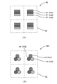
- FIG. 2A is an enlarged plan view of a part of the mounting structure of the present disclosure
- FIG. 2B is an enlarged plan view of a part of a modification of the mounting structure of the present disclosure.
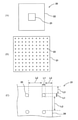
- 3A is a plan view of the master mold
- FIG. 3B is a partially enlarged plan view of FIG. 3A
- FIG. 3C is a part of FIG. 3B.
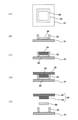
- 4 (A) to 4 (E) are schematic views showing an example of a mold forming method.
- 5 (A) to 5 (E) are schematic views showing an example of transcription by the microcontact printing method.
- 6 (A) to 6 (E) are schematic views showing the mounting method of the present disclosure.
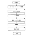
- FIG. 7 is a flowchart showing the implementation method of the present disclosure.
- the semiconductor element 11 has a terminal 14, and the substrate 12 has an electrode 15.
- the semiconductor element 11 is mounted on the substrate 12 so that the terminal 14 and the electrode 15 face each other.
- the joining portion 13 joins the terminal 14 and the electrode 15. That is, the plurality of semiconductor elements 11 are mounted on the substrate 12 via the joint portion 13.
- the semiconductor element 11 is an electronic component using a semiconductor, and here, a microscale element is particularly shown.
- the semiconductor element 11 includes a semiconductor element 111, a semiconductor element 112, and a semiconductor element 113.
- the semiconductor element 111 is a red micro LED
- the semiconductor element 112 is a green micro LED
- the semiconductor element 113 is a blue micro LED.
- One pixel is composed of one semiconductor element 111, one semiconductor element 112, and one semiconductor element 113.
- a plurality of pixels including the semiconductor element 111, the semiconductor element 112, and the semiconductor element 113 are arranged and arranged on the substrate 12 at predetermined intervals.
- the semiconductor element 11 exemplifies three types of micro LEDs in the present embodiment, they may all be the same depending on the specifications, and may include a plurality of types other than the three types. good. Further, the size, shape, number of elements, and the like may differ depending on the brightness and the like of each semiconductor element. For example, one pixel may be formed by a combination of four semiconductor elements 11 in which two semiconductor elements 113 are used for each of the semiconductor element 111 and the semiconductor element 112.
- the length of the longest line of the lines connecting arbitrary two points on the outer circumference of the semiconductor element 11 in a plan view is 100 ⁇ m or less.
- the plan view refers to a case where the substrate 12 and the like are viewed from a direction perpendicular to the plane direction.
- the semiconductor element 11 (111, 112, 113) has, for example, a rectangular shape having a diagonal line of 100 ⁇ m or less in a plan view.
- the diagonal line is more preferably 70 ⁇ m or less, and further preferably 35 ⁇ m or less.
- the joint portion 13 is formed, for example, by heat-sealing metal nanoparticles made of the above-mentioned metal.
- the temperature is preferably 100 to 200 ° C, more preferably 100 to 150 ° C, and even more preferably 100 to 120 ° C.
- the heating time is preferably 120 minutes or less, more preferably 15 minutes or less, and even more preferably 5 minutes or less.
- the joint portion 13 may be mixed and integrated with a part of the terminal 14 and the electrode 15 melted by heat fusion. As a result, the terminal 14 can be more firmly bonded to the electrode 15.
- the copper complex composition contains, for example, a first copper complex formed of ketoic acid and copper ions, and a second copper complex formed of a ligand containing a nitrogen atom and copper ions. It is preferably a thing.
- the first copper complex is preferably formed from, for example, keto acid and copper ions (copper ketoate).
- the first copper complex include copper ⁇ -ketoate such as copper glyoxylate, copper ⁇ -keto acid and copper ⁇ -ketoate.
- the first copper complex may be one of these or a combination of two or more.
- the second copper complex is preferably formed from a ligand containing a nitrogen atom and a copper ion.
- the second copper complex is, for example, a monoalkylamine copper complex (C n H 2n + 1 NH 2 Cu: n is an integer) such as a methylamine copper complex or an ethylamine copper complex, a dialkylamine copper complex, or a trialkylamine copper complex.
- Amine-based copper complexes such as ethylenediamine copper complex and ethanolamine copper complex can be mentioned.
- the second copper complex may be one of these or a combination of two or more.
- the content of the first copper complex and the second copper complex contained in the copper complex composition is not particularly limited, but is preferably in the range of 90% by weight to 5% by weight, for example, 80% by weight of the entire composition. More preferably, it is in the range of% to 10% by weight.
- the molar ratio of the first copper complex to the second copper complex (first copper complex: second copper complex) contained in the copper complex composition is not particularly limited, but is, for example, 9: 1 to 1: 1. It is preferably in the range of 9, and more preferably in the range of 8: 2 to 2: 8.
- the metal complex composition may further contain a solvent capable of dissolving the metal complex contained in the metal complex composition.
- a solvent capable of dissolving the metal complex contained in the metal complex composition.
- examples of such a solvent include alcohol solvents such as methanol, ethanol and aminoethanol, ketone solvents such as cyclohexanone, amide solvents such as dimethylformamide, terpen solvents such as terpineol, and ester solvents. ..
- the solvent may be one of the above solvents or a combination of two or more.
- the metal complex composition may contain additives other than the metal complex and the medium, if necessary. Examples of the additive include a viscosity regulator, a pH regulator and the like.
- metal nanoparticles generated by precipitation melt and grow with each other in the laser irradiation region.
- the reaction of precipitating metal nanoparticles from a metal complex proceeds in an extremely short time. That is, extremely small size metal nanoparticles are deposited before the metal complex reacts with oxygen in the atmosphere. Therefore, it is presumed that metal nanoparticles can be satisfactorily formed from the metal complex composition without being easily affected by oxidation even in the atmosphere. Further, since the precipitated metal nanoparticles are melted at a temperature lower than the melting point of the metal, the metal nanoparticles can be precipitated with low energy. Further, since the metal complex composition is in a state in which the metal complex is dissolved, problems such as aggregation and oxidation are less likely to occur as compared with a material using metal particles, and the metal complex composition is excellent in storage stability.
- the metal nanoparticles deposited on the electrode 15 are heat-sealed. As a result, the joint portion 13 is formed.
- the joining portion 13 joins the terminal 14 and the electrode 15.
- the semiconductor element 11 is mounted on the substrate 12. Further, since a plurality of joint portions 13 are formed at one time by using a microcontact printing method, the semiconductor element 11 can be efficiently and accurately mounted on the substrate 12.
- the mounting structure 10 of the present disclosure can be preferably used as, for example, an LED (including an LED display), a display element for a head-up display, a backlight such as a liquid crystal display, lighting, and an optical component such as a visible light communication device. ..
- the semiconductor element 11 can be mounted on the substrate 12 efficiently and accurately, it can be particularly preferably used as a micro LED or the like which is a miniaturized device.
- the longest line for example, the diameter in the case of a circle
- the lines connecting arbitrary two points on the outer circumference of the LED element in a plan view may be 100 ⁇ m or less.
- FIG. 3 (A) is a plan view of the master mold 20
- FIG. 3 (B) is an enlarged plan view of the transfer portion 21 which is a part of FIG. 3 (A)
- FIG. 3 (C) is a plan view. It is a plan view which further enlarged a part of the transfer part 21 of FIG. 3 (B).
- the master mold 20 is a mold for forming a mold used in the microcontact printing method.
- the master mold 20 is provided with a pattern shape (inverted shape of a desired mold) having an inverted concave-convex shape corresponding to the desired shape in order to give the mold a desired shape.
- the master mold 20 is a structure in which fine uneven shapes are applied to the surface of Si, quartz, metal, etc., and is very expensive, which is also called a master. Since a mold is formed from an expensive master mold and a pattern is formed by a microcontact printing method using the mold, the cost can be significantly reduced.
- the master mold 20 includes a transfer portion 21 and a peripheral portion 22.
- the outer shapes of the transfer portion 21 and the peripheral portion 22 are rectangular in a plan view, and the peripheral portion 22 surrounds the periphery of the transfer portion 21.
- the length of one side of the master mold 20 (the length of one side on the outer periphery of the peripheral portion 22) is preferably 10 to 700 mm, more preferably 10 to 150 mm, still more preferably 10 to 100 mm. ..
- the length of one side of the transfer unit 21 is preferably 10 to 600 mm, more preferably 10 to 100 mm, and even more preferably 10 to 50 mm.
- the shapes of the transfer portion 21 and the peripheral portion 22 are not limited to the rectangular shape, and may be adopted according to specifications such as other polygonal shapes, circular shapes, and elliptical shapes.
- the diameter (L1) of the recess 23 in a plan view is preferably 100 ⁇ m or less, more preferably 50 ⁇ m or less, still more preferably 10 ⁇ m or less. ..
- the depth of the recess 23 is preferably 200 ⁇ m or less, more preferably 100 ⁇ m or less, and even more preferably 20 ⁇ m or less.
- the distance (L2) between the recesses 23 of the transfer unit 21 is designed according to the layout of each color of the semiconductor element 11 (111, 112, 113). Further, the distance between the recesses 23 of the transfer unit 21 can be appropriately changed according to the specifications of the mounting structure 10. For example, when the master mold 20 and the substrate 12 are overlapped with each other, the recess 23 is formed at a position where it overlaps with all the electrodes 15 on the substrate 12 or at a position where it overlaps with at least a part of the electrodes 15.
- the metal complex composition is transferred onto the terminal 14 on the semiconductor element 11 side
- the recess 23 overlaps all the terminals 14 on the semiconductor element 11. It is formed at a position or a position overlapping at least a part of the terminal 14. Since there are a plurality of semiconductor elements 11, it is preferable that the semiconductor elements 11 are treated as if they are loaded on a chip plate, for example.
- the shortest distance (L3) from the edge 24 of the transfer portion 21 of the recess 23 is preferably 100 ⁇ m or less, preferably 30 ⁇ m or less, and even more preferably 10 ⁇ m or less.
- the mold of the present disclosure (hereinafter, also simply referred to as a mold) is made of a cured product or a solidified product of a resin composition (hereinafter, also referred to as a mold-forming resin composition) that forms a mold.
- the mold is, for example, a film made of a cured product or a solidified product of the resin composition forming the mold.
- the mold may be a structure in which a cured product or a solidified product of the resin composition for forming a mold is laminated on a base member.
- a mold containing a fibrous core material can be mentioned.
- the base member includes a fibrous core material and supports a cured product or a solidified product of the mold-forming resin composition.
- the cured product or solidified product of the resin composition for mold formation has an uneven shape on its surface.
- the mold is provided with a pattern shape having an inverted uneven shape corresponding to the shape of the master mold 20 by the master mold 20.
- a plurality of convex portions are formed in the locations corresponding to the plurality of concave portions 23 in the locations corresponding to the transfer portions 21 of the master mold 20 in the mold.
- the mold-forming resin composition includes a resin for forming a mold and a curable composition.
- the mold it is preferable to use a film having a linear expansion rate of 200 ppm / K or less and whose size does not change before and after repeated use with a solvent, or a mold containing a fibrous core material.
- the linear expansion rate of the mold is more preferably 100 ppm / K or less, and further preferably 50 ppm / K or less.
- the linear expansion rate of the mold is 200 ppm / K or less, the volume change due to the heat of the mold is small. Therefore, deformation of the mold due to heat generated by friction is suppressed, and transfer with higher accuracy becomes possible when used in the microcontact printing method.
- the size change before and after repeated use with a solvent can be obtained by comparing the dimensions of the initial mold with the dimensions of the mold after repeated use with a solvent.
- the dimensions of the mold after being impregnated with the solvent at room temperature for 1 hour and then dried under reduced pressure (10 Pa, 80 ° C., 2 hours) may be tentatively used.
- examples of the mold containing the fibrous core material include a mold in which a mold portion having a concavo-convex pattern shape is laminated on a fibrous core material hardened with a resin similar to the mold.
- examples of the fibrous core material include fabrics containing a material having low elasticity. Specific examples thereof include non-woven fabrics made of cellulose, cotton and the like, and woven fabrics such as glass cloth.
- the resin forming the mold examples include polysiloxane (dimethylpolysiloxane, etc.), which is a silicone-based resin, fluororesin, polyolefin-based resin (polyethylene, polypropylene, polycyclic olefin, etc.), polyethersulfone-based resin, and polycarbonate.
- polysiloxane dimethylpolysiloxane, etc.
- fluororesin polyolefin-based resin
- polyolefin-based resin polyethylene, polypropylene, polycyclic olefin, etc.
- polyethersulfone-based resin examples include based resins, polyester resins (polyarylate, polyethylene terephthalate, polyethylene naphthalate, etc.), polyamide resins, polymethyl methacrylate and the like.
- polysiloxane is preferable. Further, in the curing of the mold-forming resin composition, for example, a three-dimensional cross-linking reaction by hydrosilylation to an unsaturated double bond, radical polymerization, an epoxy reaction, or the like may be used.
- the curable composition include polysiloxane containing an epoxy compound and the like.
- polysiloxane is used as the resin, the compatibility with a curable composition such as an epoxy compound is excellent, and the contact angle tends to be small. Further, when polysiloxane is used as the resin and the curable composition, the flexibility of the obtained mold is excellent.
- a mold release agent may be added to the mold forming resin composition, and for example, an organic solvent may be added to adjust the viscosity.
- organic solvent include saturated or unsaturated hydrocarbon solvents such as pentane, hexane, heptane, octane and petroleum ether; aromatic hydrocarbon solvents such as benzene, toluene and xylene; acetone, methyl ethyl ketone and methyl isobutyl ketone.
- the viscosity (at 25 ° C.) of the mold-forming resin composition is preferably adjusted to, for example, about 1 to 100 mPa ⁇ s from the viewpoint of coatability.
- FIGS. 4 (A) and 4 (B) are schematic views showing an example of a mold forming method.
- 4 (A) is a schematic plan view
- FIG. 4 (B) is a schematic cross-sectional view of FIG. 4 (A).
- a mold set in which the master mold 20 is set is prepared.
- the master mold 20 and the frame 32 are arranged on the plate 31.
- the master mold 20, the plate 31, and the frame 32 each have a square shape in a plan view, but this is an example and is not limited to this shape.
- the mold forming resin composition 34 is filled up to the upper edge of the frame 32, so that a mold having a desired thickness can be obtained.
- the plate 31 is preferably in the shape of a flat plate, and is installed so that the surface direction is horizontal. As a result, a mold in which unnecessary thickness deviation is suppressed in the horizontal direction can be obtained.
- the material of the plate 31 is preferably one having excellent heat resistance, for example, an inorganic material such as glass or silicon; a resin such as a cycloolefin polymer, a polycarbonate, polypropylene, polyethylene or an epoxy; a metal; these materials. Combinations and the like can be mentioned.
- the material of the frame 32 is preferably one having heat resistance and chemical resistance, and examples thereof include fluororesins such as Teflon (registered trademark) and cycloolefin polymers.
- the surface of the frame 32 may be mold-released with a fluorine-based silane coupling agent or the like, if necessary.
- the above-mentioned mold forming resin composition 34 is poured into the space surrounded by the frame 32 on the master mold 20 of the mold set.
- the mold forming resin composition 34 is filled in the space surrounded by the master mold 20 and the frame 32.
- the mold-forming resin composition 34 laminated with the plate 31, the master mold 20, and the base member 35 is cured through a curing step.
- the mold-forming resin composition 34 can be cured by advancing the polymerization reaction of the curable compound (particularly, the cationically curable compound) contained in the mold-forming resin composition 34.
- the curing method can be appropriately selected from a well-known or conventional method. Although not particularly limited, examples thereof include a method of heating and / or irradiating with active energy rays.
- UV rays are preferable because they are easy to handle.
- a light source for irradiating ultraviolet rays a high-pressure mercury lamp, an ultra-high-pressure mercury lamp, a carbon arc lamp, a xenon lamp, a metal halide lamp, or the like is used.
- the formed mold 30 can be taken out by removing it from the plate 31, the frame 32, and the master mold 20. As a result, the mold 30 is obtained.
- the mold is a film made of a cured product of the mold forming resin composition 34
- the same member as the plate 31 is used instead of the base member 35 in the above-mentioned mold forming method.
- the cured mold-forming resin composition 34 can be taken out by removing it from the same members as the plate 31, the frame 32, the master mold 20, and the plate 31. As a result, a mold which is a film made of a cured product of the mold forming resin composition 34 can be obtained.
- the mold 30 is peeled off from the flat plate 41.
- the metal complex composition 42 is separated from the flat plate 41 in a state of being adsorbed on the convex portion 44 of the mold 30.
- the mold 30 is pressed against the substrate 12 having the electrode 15. It is preferable that the electrode 15 is arranged on the substrate 12 at a position facing the convex portion 44 when facing the mold 30.
- the electrode 15 may be arranged at a position facing all the convex portions 44, or, if necessary, at a position facing a part of the convex portions 44.
- the transfer rate, transfer accuracy and misalignment indicating the transferability of the transfer pattern obtained by the above transfer method satisfy the following criteria.
- Each transfer pattern is evaluated based on the observation result of the optical microscope.
- the misalignment is preferably 10 ⁇ m or less, more preferably 6 ⁇ m or less, further preferably 2 ⁇ m or less, and most preferably 0 ⁇ m, that is, there is no misalignment at all.
- the metal complex composition 42 can be accurately transferred to a plurality of locations on the electrode 15 at one time.
- the misalignment is calculated by substituting the observation result into the following equation (3).
- Positional deviation center point of transfer pattern-center point on setting ... Equation (3)
- the center point of the transfer pattern is the center position of the transferred dot pattern.
- the center point on the setting is the center position of the dot pattern when the transfer is performed accurately and without deviation.
- the positional deviation between the electrode 15 or the terminal 14 and the joint portion 13 is preferably 10 ⁇ m or less, more preferably 6 ⁇ m or less, further preferably 2 ⁇ m or less, that is, the positional deviation is 0 ⁇ m. Most preferably none at all.
- the convex portion 44 of the mold 30 When the convex portion 44 of the mold 30 is overlapped with the mold 30, it overlaps with a part of a plurality of LED elements 62 of the LED chip plate 61 in a plan view.
- the convex portion 44 is formed so as to overlap only the LED element 62 at the position where the R LED element is required.
- the mold 30 is pressed against the LED chip plate 61, the convex portion 44 can come into contact with the portion where the LED element of R is required. After that, the mold 30 is peeled off from the LED chip plate 61.
- the LED chip plate 61 is pressed against the substrate 12 having the electrode 15 (S4 in FIG. 7).
- the plurality of LED elements 62 at the location where the metal nanoparticle cluster 47 is formed come into contact with the electrodes 15 at the corresponding locations.
- the terminal 14 on the LED element 62 is in contact with the electrode 15 on the substrate 12 via the metal nanoparticle group 47.
- the terminal 14 and the electrode 15 are in contact with each other so as to sandwich the metal nanoparticle group 47 containing the metal nanoparticles.
- a frame made of Teflon (registered trademark), inner diameter: a square with a side of 20 mm in a plan view, thickness in the stacking direction: 3 mm
- the prepared liquid polysiloxane composition 1 was poured into the space surrounded by the master mold and the frame. After degassing the poured liquid polysiloxane composition 1 under reduced pressure (pressure 10 kPa) for 30 minutes, the glass substrate is placed on the liquid polysiloxane composition 1 so that bubbles do not enter between the liquid polysiloxane composition 1 and the liquid polysiloxane composition 1. I stuck it on the top of.
- a film-shaped mold (A) having a film thickness of 2 mm was obtained in which a pillar-shaped pattern (diameter of convex pattern: 10 ⁇ m, height of convex portion: 10 ⁇ m) was formed on the surface.
- the master mold is fixed on a glass substrate, and a frame (made of Teflon (registered trademark), inner diameter: a square with a side of 20 mm in a plan view, thickness in the stacking direction: 2) so as to surround the master mold. .0 mm) was fixed on the glass substrate.
- the prepared liquid polysiloxane composition 1 was poured into the space surrounded by the master mold and the frame. After degassing under reduced pressure, the prepared sheet-shaped molded base material was attached to the upper part of the liquid polysiloxane composition 1 so that bubbles did not enter between the liquid polysiloxane composition 1 and the liquid polysiloxane composition 1.
- the glass substrate, the frame, and the master mold are peeled off to form a mold (B) (thickness in the stacking direction (sheet-like mold base material and the cured product of the liquid polysiloxane composition 1).
- the place where is laminated 1.5 mm was obtained.
- Transfer example 2 Copper nanoparticles were precipitated by transfer and transfer of the copper complex composition A by the same operation as in Transfer Example 1 except that the mold (B) of Production Example 2 was used, and the copper nanoparticles formed on the glass substrate were contained. The transfer pattern (B) to be used was obtained.
- Transfer rate (%) number of dots transferred in 10 ⁇ 10 at the center of the transfer pattern / 100 ⁇ 100 ... Equation (1)
- the transferability at the transfer rate was evaluated according to the following evaluation criteria. ⁇ : Transfer rate is 98% or more: (Good transferability)
- X Transfer rate is less than 98%: (Poor transferability)
- ⁇ Position shift> The positional deviation of the obtained transfer pattern was calculated by substituting it into the following equation (3).
- Positional deviation center point of transfer pattern-center point on setting ... Equation (3)
- the center point of the transfer pattern is the center position of the transferred dot pattern.
- the center point on the setting is the center position of the dot pattern when the transfer is performed accurately and without deviation.
- the transferability in misalignment was evaluated according to the following evaluation criteria. ⁇ : Positional deviation ⁇ 2 ⁇ m (excellent transferability) ⁇ : 2 ⁇ m ⁇ Position deviation ⁇ 10 ⁇ m (good transferability) X: 10 ⁇ m ⁇ Position shift (poor transferability)
- the copper plate was placed on a glass substrate having copper bumps having the same pattern shape as Master Mold.
- the copper bumps on the glass substrate are laminated so as to face each other with the transferred transfer pattern on the copper plate.
- the laminated glass substrate and copper plate were heated at 200 ° C. for 30 minutes.
- the copper nanoparticles in the transfer pattern are heat fused with the copper bumps on the glass substrate.
- the copper plate was joined to the copper bump on the glass substrate.
- the bonded state was observed from the glass surface with an optical microscope (DM4000M, manufactured by Leica Microsystems, Inc.). From the observation results of the optical microscope, it was confirmed that the copper plate was bonded to the copper bumps on the glass substrate.
- a semiconductor element having terminals is a mounting structure mounted on a substrate having electrodes.
- the mounting structure includes a joint portion in which the terminal and the electrode are joined so as to face each other.
- the electrodes are bumps of bulk metal material placed on the substrate.
- the junction is formed by heat-sealing metal nanoparticles precipitated by laser irradiation treatment from a metal complex transferred onto at least one of the electrodes or terminals using a microcontact printing method.
- Mounting structure [Appendix 2] The mounting structure according to Annex 1, wherein the metal complex contains a copper complex.
- the copper complex includes a first copper complex formed of ketoic acid and copper ions, and a second copper complex formed of a ligand containing a nitrogen atom and copper ions.
- the mounting structure described in. [Appendix 4] The total content of the first copper complex and the second copper complex is 90% by weight to 5% by weight (preferably 80% by weight to 10% by weight) of the entire composition forming the metal complex. ), The mounting structure according to Appendix 3.
- the molar ratio of the first copper complex to the second copper complex is 9: 1 to 1: 9 (preferably 8: 2 to 2). : The mounting structure according to Appendix 3 or 4, which is within the range of 8).
- the mold used in the microcontact printing method has a linear expansion rate of 200 ppm / K or less (preferably 100 ppm / K or less, more preferably 50 ppm / K or less) before and after repeated use with a solvent.
- the mounting structure according to any one of Supplementary note 1 to 8, wherein a mold made of a film whose size does not change in the above method or a mold containing a fibrous core material (preferably a polysiloxane mold containing the fibrous core material) is used. body.
- the mold containing the fibrous core material is a mold in which a mold portion having a concavo-convex pattern shape is laminated on a fibrous core material hardened with a resin (preferably polysiloxane).
- the mounting structure according to Appendix 10 wherein the fibrous core material hardened with the resin has a structure in which the fibrous core material is impregnated with the resin.
- the metal complex includes a cuprous complex formed from keto acid and copper ions, and a cupric complex formed from a ligand containing a nitrogen atom and copper ions.
- the mounting method described in. [Appendix 20] The total content of the first copper complex and the second copper complex is 90% by weight to 5% by weight (preferably 80% by weight to 10% by weight) of the entire composition forming the metal complex. ), The implementation method according to Appendix 19.
- the molar ratio of the first copper complex to the second copper complex is 9: 1 to 1: 9 (preferably 8: 2 to 2). : The mounting method according to Appendix 19 or 20, which is within the range of 8).
Landscapes
- Engineering & Computer Science (AREA)
- Microelectronics & Electronic Packaging (AREA)
- Manufacturing & Machinery (AREA)
- Led Device Packages (AREA)
- Wire Bonding (AREA)
- Electric Connection Of Electric Components To Printed Circuits (AREA)
Priority Applications (5)
| Application Number | Priority Date | Filing Date | Title |
|---|---|---|---|
| US18/019,434 US20240038951A1 (en) | 2020-09-07 | 2021-09-02 | Mounted structure, led display, and mounting method |
| KR1020237011534A KR20230062614A (ko) | 2020-09-07 | 2021-09-02 | 실장 구조체, led 디스플레이 및 실장 방법 |
| CN202180050332.9A CN115956289A (zh) | 2020-09-07 | 2021-09-02 | 安装构造体、led显示器以及安装方法 |
| JP2022546970A JPWO2022050354A1 (https=) | 2020-09-07 | 2021-09-02 | |
| EP21864407.8A EP4213196A4 (en) | 2020-09-07 | 2021-09-02 | MOUNTING STRUCTURE, LED DISPLAY AND MOUNTING METHOD |
Applications Claiming Priority (2)
| Application Number | Priority Date | Filing Date | Title |
|---|---|---|---|
| JP2020-150004 | 2020-09-07 | ||
| JP2020150004 | 2020-09-07 |
Publications (1)
| Publication Number | Publication Date |
|---|---|
| WO2022050354A1 true WO2022050354A1 (ja) | 2022-03-10 |
Family
ID=80491117
Family Applications (1)
| Application Number | Title | Priority Date | Filing Date |
|---|---|---|---|
| PCT/JP2021/032305 Ceased WO2022050354A1 (ja) | 2020-09-07 | 2021-09-02 | 実装構造体、ledディスプレイ、及び実装方法 |
Country Status (7)
| Country | Link |
|---|---|
| US (1) | US20240038951A1 (https=) |
| EP (1) | EP4213196A4 (https=) |
| JP (1) | JPWO2022050354A1 (https=) |
| KR (1) | KR20230062614A (https=) |
| CN (1) | CN115956289A (https=) |
| TW (1) | TW202224212A (https=) |
| WO (1) | WO2022050354A1 (https=) |
Families Citing this family (2)
| Publication number | Priority date | Publication date | Assignee | Title |
|---|---|---|---|---|
| US20230420269A1 (en) * | 2022-06-27 | 2023-12-28 | Nichia Corporation | Conductive paste, wiring substrate, light-emitting device,and manufacturing method thereof |
| EP4625042A1 (en) * | 2024-03-28 | 2025-10-01 | Université d'Aix Marseille | Direct metal nanoimprint |
Citations (9)
| Publication number | Priority date | Publication date | Assignee | Title |
|---|---|---|---|---|
| JPH07212015A (ja) * | 1994-01-12 | 1995-08-11 | Matsushita Electric Ind Co Ltd | 電子部品実装方法および電子部品実装機 |
| JP2004277868A (ja) * | 2003-03-19 | 2004-10-07 | Mitsubishi Paper Mills Ltd | 導電性組成物の作製方法 |
| JP2007110054A (ja) | 2005-10-17 | 2007-04-26 | Hyogo Prefecture | パターン形成方法およびパターン形成ずみ基板 |
| JP2010003854A (ja) * | 2008-06-19 | 2010-01-07 | Seiko Epson Corp | 接合膜付き回路基板、接合膜付き回路基板の接合方法、電子デバイスおよび電子機器 |
| JP4539284B2 (ja) | 2004-10-26 | 2010-09-08 | パナソニック株式会社 | 発光素子実装構造体および発光素子実装構造体の製造方法 |
| JP2010278228A (ja) * | 2009-05-28 | 2010-12-09 | Seiko Epson Corp | 接合方法および接合体 |
| JP2012119572A (ja) * | 2010-12-02 | 2012-06-21 | Shimadzu Corp | 転写印刷用スタンプ製造方法および電子デバイス |
| WO2018212345A1 (ja) | 2017-05-18 | 2018-11-22 | 学校法人芝浦工業大学 | 導体の製造方法、配線基板の製造方法及び導体形成用組成物 |
| JP2020150004A (ja) | 2019-03-11 | 2020-09-17 | セイコーインスツル株式会社 | パッケージ及びパッケージの製造方法 |
Family Cites Families (8)
| Publication number | Priority date | Publication date | Assignee | Title |
|---|---|---|---|---|
| JP2009164261A (ja) * | 2007-12-28 | 2009-07-23 | Seiko Epson Corp | 半導体装置および電子機器 |
| JP2010219447A (ja) * | 2009-03-18 | 2010-09-30 | Toppan Printing Co Ltd | 有機トランジスタ用インク、有機トランジスタの電極及びその形成方法並びに有機トランジスタ |
| WO2013146483A1 (ja) * | 2012-03-30 | 2013-10-03 | 帝人株式会社 | 透明導電性積層体 |
| JP2014013868A (ja) * | 2012-07-05 | 2014-01-23 | Nec Corp | マイクロコンタクトプリント装置およびマイクロコンタクトプリント方法 |
| JP2016167471A (ja) * | 2013-07-09 | 2016-09-15 | 株式会社ダイセル | 銀ナノ粒子を用いた半導体装置及びその製造方法 |
| KR20160054339A (ko) * | 2014-11-06 | 2016-05-16 | 주식회사 실리콘웍스 | 개선된 패턴을 가지는 기판 및 집적회로 칩 |
| FR3039008B1 (fr) | 2015-07-16 | 2019-06-14 | Safran Electrical & Power | Dispositif de connexion electrique raccordable a plusieurs cables avec protection contre les dommages par corps etrangers |
| TW202541302A (zh) * | 2019-02-04 | 2025-10-16 | 日商索尼半導體解決方案公司 | 電子裝置 |
-
2021
- 2021-09-02 CN CN202180050332.9A patent/CN115956289A/zh active Pending
- 2021-09-02 US US18/019,434 patent/US20240038951A1/en active Pending
- 2021-09-02 KR KR1020237011534A patent/KR20230062614A/ko not_active Ceased
- 2021-09-02 EP EP21864407.8A patent/EP4213196A4/en not_active Withdrawn
- 2021-09-02 JP JP2022546970A patent/JPWO2022050354A1/ja active Pending
- 2021-09-02 WO PCT/JP2021/032305 patent/WO2022050354A1/ja not_active Ceased
- 2021-09-07 TW TW110133219A patent/TW202224212A/zh unknown
Patent Citations (9)
| Publication number | Priority date | Publication date | Assignee | Title |
|---|---|---|---|---|
| JPH07212015A (ja) * | 1994-01-12 | 1995-08-11 | Matsushita Electric Ind Co Ltd | 電子部品実装方法および電子部品実装機 |
| JP2004277868A (ja) * | 2003-03-19 | 2004-10-07 | Mitsubishi Paper Mills Ltd | 導電性組成物の作製方法 |
| JP4539284B2 (ja) | 2004-10-26 | 2010-09-08 | パナソニック株式会社 | 発光素子実装構造体および発光素子実装構造体の製造方法 |
| JP2007110054A (ja) | 2005-10-17 | 2007-04-26 | Hyogo Prefecture | パターン形成方法およびパターン形成ずみ基板 |
| JP2010003854A (ja) * | 2008-06-19 | 2010-01-07 | Seiko Epson Corp | 接合膜付き回路基板、接合膜付き回路基板の接合方法、電子デバイスおよび電子機器 |
| JP2010278228A (ja) * | 2009-05-28 | 2010-12-09 | Seiko Epson Corp | 接合方法および接合体 |
| JP2012119572A (ja) * | 2010-12-02 | 2012-06-21 | Shimadzu Corp | 転写印刷用スタンプ製造方法および電子デバイス |
| WO2018212345A1 (ja) | 2017-05-18 | 2018-11-22 | 学校法人芝浦工業大学 | 導体の製造方法、配線基板の製造方法及び導体形成用組成物 |
| JP2020150004A (ja) | 2019-03-11 | 2020-09-17 | セイコーインスツル株式会社 | パッケージ及びパッケージの製造方法 |
Non-Patent Citations (1)
| Title |
|---|
| See also references of EP4213196A4 |
Also Published As
| Publication number | Publication date |
|---|---|
| TW202224212A (zh) | 2022-06-16 |
| JPWO2022050354A1 (https=) | 2022-03-10 |
| EP4213196A4 (en) | 2024-11-20 |
| CN115956289A (zh) | 2023-04-11 |
| EP4213196A1 (en) | 2023-07-19 |
| KR20230062614A (ko) | 2023-05-09 |
| US20240038951A1 (en) | 2024-02-01 |
Similar Documents
| Publication | Publication Date | Title |
|---|---|---|
| TWI527848B (zh) | 非隨機異方性導電膠膜及其製程 | |
| US8250750B2 (en) | Method for manufacturing tape wiring board | |
| CN108419378B (zh) | 印刷线路板保护层的制作方法 | |
| CN1444270A (zh) | Cof柔性印刷线路板及制造该线路板的方法 | |
| WO2022050354A1 (ja) | 実装構造体、ledディスプレイ、及び実装方法 | |
| CN1532905A (zh) | 电子部件的制造方法、电子部件、电子部件的安装方法和电子装置 | |
| CN105102514B (zh) | 用于激光烧蚀的具有图像增强的微孔载体 | |
| TWI304608B (en) | Manufacturing method of semiconductor device, semiconductor device, circuit board, electro-optic device, and electronic apparatus | |
| JP6032637B2 (ja) | 部品実装基板の製造システム及び製造方法 | |
| WO2022050353A1 (ja) | 実装構造体、ledディスプレイ、及び実装方法 | |
| CN100401860C (zh) | 图案形状物及其制造方法 | |
| US9468095B1 (en) | Manufacturing method of multilayer wiring and multilayer wiring structure | |
| JP4137177B2 (ja) | 導電パターンの形成方法、および配線基板 | |
| CN101573784B (zh) | 电极结构体及凸点形成方法 | |
| KR20220122663A (ko) | 땜납 범프 형성용 부재, 땜납 범프 형성용 부재의 제조 방법, 및 땜납 범프 부착 전극 기판의 제조 방법 | |
| KR20140037635A (ko) | 도전성 페이스트를 충진시켜서 회로기판을 제작하는 방법과 그 방법에 의하여 제작된 회로기판 | |
| CN109302806B (zh) | 一种线路板的制备方法 | |
| JP2014017534A (ja) | 配線板の製造方法 | |
| JP5406241B2 (ja) | 配線板の製造方法 | |
| CN108174522A (zh) | 一种嵌埋线路柔性电路板及其制备方法 | |
| CN111403362A (zh) | 覆晶薄膜封装方法、封装结构、显示装置、电子设备 | |
| KR101886303B1 (ko) | 나노구조의 미세패턴을 갖는 실리카 박막 제조방법 | |
| JP6671335B2 (ja) | 機能性膜のパターニング方法、電子デバイスの製造方法 | |
| KR20200001842A (ko) | 나노패턴을 포함하는 바코터 및 그 제조방법, 바코터를 이용한 박막 형성방법 | |
| TW202130764A (zh) | 用於圖案化預成型物之製造及膠帶轉移方法 |
Legal Events
| Date | Code | Title | Description |
|---|---|---|---|
| 121 | Ep: the epo has been informed by wipo that ep was designated in this application |
Ref document number: 21864407 Country of ref document: EP Kind code of ref document: A1 |
|
| WWE | Wipo information: entry into national phase |
Ref document number: 18019434 Country of ref document: US |
|
| ENP | Entry into the national phase |
Ref document number: 2022546970 Country of ref document: JP Kind code of ref document: A |
|
| ENP | Entry into the national phase |
Ref document number: 20237011534 Country of ref document: KR Kind code of ref document: A |
|
| NENP | Non-entry into the national phase |
Ref country code: DE |
|
| ENP | Entry into the national phase |
Ref document number: 2021864407 Country of ref document: EP Effective date: 20230411 |
|
| WWW | Wipo information: withdrawn in national office |
Ref document number: 2021864407 Country of ref document: EP |
|
| WWR | Wipo information: refused in national office |
Ref document number: 1020237011534 Country of ref document: KR |