WO2022050353A1 - 実装構造体、ledディスプレイ、及び実装方法 - Google Patents
実装構造体、ledディスプレイ、及び実装方法 Download PDFInfo
- Publication number
- WO2022050353A1 WO2022050353A1 PCT/JP2021/032303 JP2021032303W WO2022050353A1 WO 2022050353 A1 WO2022050353 A1 WO 2022050353A1 JP 2021032303 W JP2021032303 W JP 2021032303W WO 2022050353 A1 WO2022050353 A1 WO 2022050353A1
- Authority
- WO
- WIPO (PCT)
- Prior art keywords
- mold
- ink
- printing method
- substrate
- metal nanoparticles
- Prior art date
- Legal status (The legal status is an assumption and is not a legal conclusion. Google has not performed a legal analysis and makes no representation as to the accuracy of the status listed.)
- Ceased
Links
Images




Classifications
-
- H—ELECTRICITY
- H10—SEMICONDUCTOR DEVICES; ELECTRIC SOLID-STATE DEVICES NOT OTHERWISE PROVIDED FOR
- H10W—GENERIC PACKAGES, INTERCONNECTIONS, CONNECTORS OR OTHER CONSTRUCTIONAL DETAILS OF DEVICES COVERED BY CLASS H10
- H10W90/00—Package configurations
- H10W90/701—Package configurations characterised by the relative positions of pads or connectors relative to package parts
-
- H—ELECTRICITY
- H10—SEMICONDUCTOR DEVICES; ELECTRIC SOLID-STATE DEVICES NOT OTHERWISE PROVIDED FOR
- H10H—INORGANIC LIGHT-EMITTING SEMICONDUCTOR DEVICES HAVING POTENTIAL BARRIERS
- H10H20/00—Individual inorganic light-emitting semiconductor devices having potential barriers, e.g. light-emitting diodes [LED]
- H10H20/01—Manufacture or treatment
- H10H20/011—Manufacture or treatment of bodies, e.g. forming semiconductor layers
- H10H20/018—Bonding of wafers
-
- B—PERFORMING OPERATIONS; TRANSPORTING
- B41—PRINTING; LINING MACHINES; TYPEWRITERS; STAMPS
- B41M—PRINTING, DUPLICATING, MARKING, OR COPYING PROCESSES; COLOUR PRINTING
- B41M1/00—Inking and printing with a printer's forme
- B41M1/02—Letterpress printing, e.g. book printing
-
- B—PERFORMING OPERATIONS; TRANSPORTING
- B41—PRINTING; LINING MACHINES; TYPEWRITERS; STAMPS
- B41M—PRINTING, DUPLICATING, MARKING, OR COPYING PROCESSES; COLOUR PRINTING
- B41M1/00—Inking and printing with a printer's forme
- B41M1/10—Intaglio printing ; Gravure printing
-
- B—PERFORMING OPERATIONS; TRANSPORTING
- B41—PRINTING; LINING MACHINES; TYPEWRITERS; STAMPS
- B41N—PRINTING PLATES OR FOILS; MATERIALS FOR SURFACES USED IN PRINTING MACHINES FOR PRINTING, INKING, DAMPING, OR THE LIKE; PREPARING SUCH SURFACES FOR USE AND CONSERVING THEM
- B41N1/00—Printing plates or foils; Materials therefor
- B41N1/003—Printing plates or foils; Materials therefor with ink abhesive means or abhesive forming means, such as abhesive siloxane or fluoro compounds, e.g. for dry lithographic printing
-
- G—PHYSICS
- G09—EDUCATION; CRYPTOGRAPHY; DISPLAY; ADVERTISING; SEALS
- G09F—DISPLAYING; ADVERTISING; SIGNS; LABELS OR NAME-PLATES; SEALS
- G09F9/00—Indicating arrangements for variable information in which the information is built-up on a support by selection or combination of individual elements
- G09F9/30—Indicating arrangements for variable information in which the information is built-up on a support by selection or combination of individual elements in which the desired character or characters are formed by combining individual elements
- G09F9/33—Indicating arrangements for variable information in which the information is built-up on a support by selection or combination of individual elements in which the desired character or characters are formed by combining individual elements being semiconductor devices, e.g. diodes
-
- H—ELECTRICITY
- H05—ELECTRIC TECHNIQUES NOT OTHERWISE PROVIDED FOR
- H05K—PRINTED CIRCUITS; CASINGS OR CONSTRUCTIONAL DETAILS OF ELECTRIC APPARATUS; MANUFACTURE OF ASSEMBLAGES OF ELECTRICAL COMPONENTS
- H05K3/00—Apparatus or processes for manufacturing printed circuits
- H05K3/10—Apparatus or processes for manufacturing printed circuits in which conductive material is applied to the insulating support in such a manner as to form the desired conductive pattern
- H05K3/20—Apparatus or processes for manufacturing printed circuits in which conductive material is applied to the insulating support in such a manner as to form the desired conductive pattern by affixing prefabricated conductor pattern
-
- H—ELECTRICITY
- H05—ELECTRIC TECHNIQUES NOT OTHERWISE PROVIDED FOR
- H05K—PRINTED CIRCUITS; CASINGS OR CONSTRUCTIONAL DETAILS OF ELECTRIC APPARATUS; MANUFACTURE OF ASSEMBLAGES OF ELECTRICAL COMPONENTS
- H05K3/00—Apparatus or processes for manufacturing printed circuits
- H05K3/30—Assembling printed circuits with electric components, e.g. with resistors
- H05K3/32—Assembling printed circuits with electric components, e.g. with resistors electrically connecting electric components or wires to printed circuits
-
- H—ELECTRICITY
- H10—SEMICONDUCTOR DEVICES; ELECTRIC SOLID-STATE DEVICES NOT OTHERWISE PROVIDED FOR
- H10H—INORGANIC LIGHT-EMITTING SEMICONDUCTOR DEVICES HAVING POTENTIAL BARRIERS
- H10H20/00—Individual inorganic light-emitting semiconductor devices having potential barriers, e.g. light-emitting diodes [LED]
- H10H20/80—Constructional details
- H10H20/85—Packages
- H10H20/857—Interconnections, e.g. lead-frames, bond wires or solder balls
-
- H—ELECTRICITY
- H10—SEMICONDUCTOR DEVICES; ELECTRIC SOLID-STATE DEVICES NOT OTHERWISE PROVIDED FOR
- H10W—GENERIC PACKAGES, INTERCONNECTIONS, CONNECTORS OR OTHER CONSTRUCTIONAL DETAILS OF DEVICES COVERED BY CLASS H10
- H10W70/00—Package substrates; Interposers; Redistribution layers [RDL]
- H10W70/60—Insulating or insulated package substrates; Interposers; Redistribution layers
-
- H—ELECTRICITY
- H10—SEMICONDUCTOR DEVICES; ELECTRIC SOLID-STATE DEVICES NOT OTHERWISE PROVIDED FOR
- H10W—GENERIC PACKAGES, INTERCONNECTIONS, CONNECTORS OR OTHER CONSTRUCTIONAL DETAILS OF DEVICES COVERED BY CLASS H10
- H10W72/00—Interconnections or connectors in packages
- H10W72/20—Bump connectors, e.g. solder bumps or copper pillars; Dummy bumps; Thermal bumps
-
- H—ELECTRICITY
- H10—SEMICONDUCTOR DEVICES; ELECTRIC SOLID-STATE DEVICES NOT OTHERWISE PROVIDED FOR
- H10W—GENERIC PACKAGES, INTERCONNECTIONS, CONNECTORS OR OTHER CONSTRUCTIONAL DETAILS OF DEVICES COVERED BY CLASS H10
- H10W90/00—Package configurations
-
- H—ELECTRICITY
- H10—SEMICONDUCTOR DEVICES; ELECTRIC SOLID-STATE DEVICES NOT OTHERWISE PROVIDED FOR
- H10H—INORGANIC LIGHT-EMITTING SEMICONDUCTOR DEVICES HAVING POTENTIAL BARRIERS
- H10H20/00—Individual inorganic light-emitting semiconductor devices having potential barriers, e.g. light-emitting diodes [LED]
- H10H20/01—Manufacture or treatment
- H10H20/036—Manufacture or treatment of packages
- H10H20/0364—Manufacture or treatment of packages of interconnections
-
- H—ELECTRICITY
- H10—SEMICONDUCTOR DEVICES; ELECTRIC SOLID-STATE DEVICES NOT OTHERWISE PROVIDED FOR
- H10W—GENERIC PACKAGES, INTERCONNECTIONS, CONNECTORS OR OTHER CONSTRUCTIONAL DETAILS OF DEVICES COVERED BY CLASS H10
- H10W70/00—Package substrates; Interposers; Redistribution layers [RDL]
- H10W70/01—Manufacture or treatment
- H10W70/05—Manufacture or treatment of insulating or insulated package substrates, or of interposers, or of redistribution layers
- H10W70/098—Applying pastes or inks, e.g. screen printing
-
- H—ELECTRICITY
- H10—SEMICONDUCTOR DEVICES; ELECTRIC SOLID-STATE DEVICES NOT OTHERWISE PROVIDED FOR
- H10W—GENERIC PACKAGES, INTERCONNECTIONS, CONNECTORS OR OTHER CONSTRUCTIONAL DETAILS OF DEVICES COVERED BY CLASS H10
- H10W72/00—Interconnections or connectors in packages
- H10W72/071—Connecting or disconnecting
- H10W72/072—Connecting or disconnecting of bump connectors
Definitions
- the present disclosure relates to a mounting structure in which a semiconductor element is mounted on a substrate, an LED display including the mounting structure, and a mounting method for mounting the semiconductor element on a substrate.
- a wet process electroless plating method or electrolytic plating method, etc.
- a metal layer formed on the entire surface of the insulating substrate by a dry process vacuum vapor deposition method, sputtering method, etc.
- a photolithograph method There is known a method (subtractive method) of forming a metal wiring by etching using a mask formed in the above process and removing the mask after the plating is completed.
- Patent Document 2 In the inkjet method of Patent Document 1, a wiring pattern is formed on the substrate by ejecting the metal nanoparticle paste from the nozzle onto the substrate and then heating the paste. Furthermore, a contact print that forms a pattern of a conductive material on a substrate by applying a paste containing conductive particles to the surface of a resin template that has been patterned including irregularities and pressing it onto a SiO 2 / Si substrate. A method has also been reported (Patent Document 2).
- the inkjet method of Patent Document 1 is a method of ejecting a metal nanoparticle paste directly from a nozzle onto a substrate. At this time, the metal nanoparticle paste may scatter, bleed, or spread on the substrate when viewed at the nano level. be. This may reduce the accuracy of the wiring pattern.
- silver nanopaste is applied on the resin template to form a layer of silver nanopaste having undulations according to unevenness on the template. After that, the template is pressed against the substrate, and only the silver nanopaste applied to the convex portion is transferred to the SiO 2 / Si substrate. Therefore, since the silver nanopaste applied to the concave portion of the template remains after transfer, it is necessary to remove the remaining silver nanopaste by washing for continuous use. Therefore, the same template cannot be used continuously, and the manufacturing efficiency may decrease.
- an object of the present disclosure is to use a mounting structure in which a semiconductor element is mounted on a substrate, an LED display including the mounting structure, and a semiconductor element as a substrate, which can be manufactured efficiently with less joint blurring and excellent accuracy. It is to provide an implementation method for implementation.
- the inventors of the present disclosure transfer using a microcontact printing method onto at least one of an electrode or a terminal which is a bump of a bulk metal material arranged on a substrate. It has been found that by heat-sealing the metal nanoparticles in the ink containing the metal nanoparticles, it is possible to obtain a mounting structure that has less bonding blur, is excellent in accuracy, and can be efficiently manufactured. This disclosure has been completed based on these findings.
- the present disclosure is a mounting structure in which a semiconductor element having terminals is mounted on a substrate having electrodes, and the mounting structure is a joint portion for joining the terminals and the electrodes so as to face each other.
- the electrode is a bump of bulk metal material placed on the substrate, and the junction is a metal nano transferred onto at least one of the electrode or terminal using a microcontact printing method.
- a mounting structure in which metal nanoparticles in an ink containing particles are heat-sealed.
- the present disclosure is a mounting method in which a semiconductor element having terminals is mounted on a substrate having electrodes, wherein the electrodes are bumps of a bulk metal material arranged on the substrate, and a microcontact printing method is used.
- the metal nanoparticles containing the metal nanoparticles are transferred onto at least one of the electrode or the terminal, and the terminal and the electrode are transferred onto at least one of the electrode or the terminal.
- a mounting method for heat-sealing in a state of contact with an ink containing an ink is provided.
- the average particle size of the metal nanoparticles is preferably 0.5 to 100 nm.
- the mold used in the above microcontact printing method preferably contains polysiloxane as a constituent material.
- the mold used in the above microcontact printing method is a film having a linear expansion rate of 200 ppm / K or less and whose size does not change before and after repeated use with a solvent, or a polysiloxane mold containing a fibrous core material. It is preferable to do so.
- the micro-contact printing method is a letterpress printing method using a mold, and an ink containing metal nanoparticles transferred onto at least one of the electrodes or terminals is applied to the ink uniformly applied to a flat plate. It is preferable that the portion that is attracted to the convex portion of the mold when the mold is pressed is transferred.
- the micro-contact printing method is an intaglio printing method using a mold, and an ink containing metal nanoparticles transferred onto at least one of the electrode or the terminal is applied to the ink uniformly applied to a flat plate. It is preferable that the ink filled in the concave portion of the mold is transferred when the mold is pressed against the mold.
- the micro-contact printing method is an offset printing method using a mold and an intermediate transfer body, and ink containing metal nanoparticles transferred onto at least one of the electrodes or terminals is transferred to the intermediate transfer body.
- the mold is pressed against the uniformly applied ink and peeled off, the ink remaining on the intermediate transfer body is transferred onto at least one of the electrodes or terminals on the substrate. Is preferable.
- the semiconductor element is preferably an LED element having the longest line length of 100 ⁇ m or less among the lines connecting arbitrary two points on the outer circumference of the semiconductor element in a plan view.
- the present disclosure provides an LED display including the above mounting structure.
- the mounting structure or mounting method of the present disclosure it is possible to obtain a mounting structure that has less joint blurring, is excellent in accuracy, and can be manufactured efficiently. Further, the mounting structure of the present disclosure can be suitably used as an LED display.
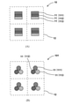
- FIG. 1 (A) is an enlarged perspective view of a part of the mounting structure of the present disclosure
- FIG. 1 (B) is a partial cross-sectional view of FIG. 1 (A).
- FIG. 2A is an enlarged plan view of a part of the mounting structure of the present disclosure
- FIG. 2B is an enlarged plan view of a part of a modification of the mounting structure of the present disclosure.
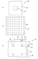
- 3A is a plan view of the master mold
- FIG. 3B is a partially enlarged plan view of FIG. 3A
- FIG. 3C is a part of FIG. 3B. It is an enlarged plan view.
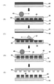
- 4 (A) to 4 (E) are schematic views showing an example of a mold forming method.
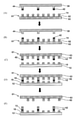
- FIG. 5 (A) to 5 (E) are schematic views showing an example of transcription by the microcontact printing method.
- 6 (A) to 6 (E) are schematic views showing another example of transcription by the microcontact printing method.
- 7 (A) to 7 (E) are schematic views showing still another example of transcription by the microcontact printing method.
- 8 (A) to 8 (E) are schematic views showing the mounting method of the present disclosure.
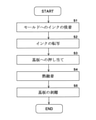
- FIG. 9 is a flowchart showing the implementation method of the present disclosure.
- FIG. 1 (A) is an enlarged perspective view of a part of the mounting structure (hereinafter, also simply referred to as a mounting structure) 10 of the present disclosure
- FIG. 1 (B) is a part of FIG. 1 (A). It is a cross-sectional view.
- FIG. 2A is an enlarged plan view of a part of the mounting structure 10
- FIG. 2B is an enlarged plan view of a part of a modified example of the mounting structure 10.
- the mounting structure 10 includes a plurality of semiconductor elements 11, a substrate 12, and a plurality of junctions 13.
- the semiconductor element 11 has a terminal 14, and the substrate 12 has an electrode 15.
- the semiconductor element 11 is mounted on the substrate 12 so that the terminal 14 and the electrode 15 face each other.
- the joining portion 13 joins the terminal 14 and the electrode 15. That is, the plurality of semiconductor elements 11 are mounted on the substrate 12 via the joint portion 13.
- the semiconductor element 11 is an electronic component using a semiconductor, and here, a microscale element is particularly shown.
- the semiconductor element 11 includes a semiconductor element 111, a semiconductor element 112, and a semiconductor element 113.
- the semiconductor element 111 is a red micro LED
- the semiconductor element 112 is a green micro LED
- the semiconductor element 113 is a blue micro LED.
- One pixel is composed of one semiconductor element 111, one semiconductor element 112, and one semiconductor element 113.
- a plurality of pixels including the semiconductor element 111, the semiconductor element 112, and the semiconductor element 113 are arranged and arranged on the substrate 12 at predetermined intervals.
- the semiconductor element 11 exemplifies three types of micro LEDs in the present embodiment, they may all be the same depending on the specifications, and may include a plurality of types other than the three types. good. Further, the size, shape, number of elements, and the like may differ depending on the brightness and the like of each semiconductor element. For example, one pixel may be formed by a combination of four semiconductor elements 11 in which two semiconductor elements 113 are used for each of the semiconductor element 111 and the semiconductor element 112.
- the length of the longest line of the lines connecting arbitrary two points on the outer circumference of the semiconductor element 11 in a plan view is 100 ⁇ m or less.
- the plan view refers to a case where the substrate 12 and the like are viewed from a direction perpendicular to the plane direction.
- the semiconductor element 11 (111, 112, 113) has a rectangular shape having a diagonal of 100 ⁇ m or less in a plan view as shown in FIG. 2 (A).
- the diagonal line is more preferably 70 ⁇ m or less, and further preferably 35 ⁇ m or less.
- FIG. 2B shows a mounting structure 101 which is a modification of the mounting structure 10.
- the semiconductor element 11 (111, 112, 113) has a circular shape having a diameter of 100 ⁇ m or less.
- the diameter is more preferably 50 ⁇ m or less, and further preferably 20 ⁇ m or less.
- the shape of the semiconductor element 11 is not limited to a rectangular shape or a circular shape, and other polygonal shapes, elliptical shapes, and the like can be adopted depending on the specifications.
- the substrate 12 is a flat substrate having an electrode 15.
- the flat substrate include a glass plate; a semiconductor such as silicon, gallium arsenic, and gallium nitride; a composite substrate obtained by impregnating a base material such as glass cloth or a non-woven fabric with a resin such as an epoxy resin and curing the composite substrate: an epoxy resin cured product, a liquid crystal.
- Engineering plastics such as polymers, resin substrates such as polycarbonate, polypropylene, and polyethylene; metal substrates; combinations of these materials and the like can be mentioned.
- the substrate 12 may have a pattern structure such as a fine wiring, a crystal structure, an optical waveguide, an optical structure such as holography, and the like, if necessary.
- the substrate 12 has, for example, a rectangular shape having a diagonal length of 600 mm or less in a plan view.
- the diagonal length is more preferably 100 mm or less, and further preferably 75 mm or less.
- the shape of the substrate 12 is not limited to a rectangular shape, and may be adopted depending on specifications such as other polygonal shapes, circular shapes, and elliptical shapes.
- the electrode 15 is a bump (convex portion) of a bulk metal material arranged on the substrate 12.
- the bulk metal material is preferably conductive and has low resistance.
- the components constituting the bulk metal material include metals, metal salts such as metal oxides, and carbon.
- the components constituting the bulk metal material may be composed of only one kind of component, or may contain a plurality of kinds of components. Among them, metal is preferable as the component constituting the bulk metal material.
- Metals are, for example, a single element such as gold, silver, palladium, platinum, nickel, copper, iron, lead, cobalt, manganese, aluminum, zinc, bismuth, silicon, tin, cadmium, indium, and multiple elements of these metals. , It may be an oxide or a salt of these metals.
- the electrode 15 is arranged on the substrate 12 according to the specifications of the mounting structure 10.
- the electrodes 15 are arranged at positions corresponding to all the semiconductor elements 11.
- the joint portion 13 contains a material having conductivity.
- the conductive material include metals, metal salts such as metal oxides, carbon and the like, or mixtures thereof.
- the metal include gold, silver, palladium, platinum, nickel, copper, iron, lead, cobalt, manganese, aluminum, zinc, bismuth, silicon, tin, cadmium, indium and the like.
- the metal is particularly preferably silver. Since silver nanoparticles are highly versatile and have a low melting point, they can be sintered at a relatively low temperature. Therefore, the temperature such as heat fusion can be maintained at a relatively low temperature, and the influence of heat on the semiconductor element 11 and the substrate 12 can be suppressed.
- the joint portion 13 is formed, for example, by heat-sealing metal nanoparticles made of the above-mentioned metal.
- the temperature is preferably 100 to 200 ° C, more preferably 100 to 150 ° C, and even more preferably 100 to 120 ° C.
- the heating time is preferably 120 minutes or less, more preferably 15 minutes or less, and even more preferably 5 minutes or less.
- the joint portion 13 may be mixed and integrated with a part of the terminal 14 and the electrode 15 melted by heat fusion. As a result, the terminal 14 can be more firmly bonded to the electrode 15.
- the metal nanoparticles are inks containing metal nanoparticles transferred onto the electrode 15 using a microcontact printing method.
- the ink containing the metal nanoparticles may be transferred onto the terminal 14 on the semiconductor element 11 side instead of the electrode 15 on the substrate 12 side. Further, the ink containing the metal nanoparticles may be transferred onto both the electrode 15 and the terminal 14. In other words, the ink containing the metal nanoparticles may be transferred onto at least one of the electrode 15 or the terminal 14.
- ink containing metal nanoparticles can be transferred to a plurality of places at a time by using the mold described below.
- the ink containing the metal nanoparticles is a solvent in which the metal nanoparticles are dispersed.
- the solvent include aliphatic hydrocarbon solvents such as pentane, hexane, heptane, octane, nonane, decane, undecane, dodecane, tridecane and tetradecane; alicyclic hydrocarbon solvents such as cyclohexane, methylcyclohexane and decalin; toluene and xylene.
- Aromatic hydrocarbon solvents such as mecitylene; methanol, ethanol, n-propanol, isopropanol, n-butanol, isobutanol, sec-butanol, tert-butanol, n-pentanol, n-hexanol, 2-ethylhexanol.
- metal nanoparticles for the formation of the junction 13 can reduce the amount used as compared to the case of using bulk metal, and the placement of the metal in fine regions using the microcontact printing method can be achieved. It will be possible. Transcription by the microcontact printing method will be described in detail later.
- the average particle diameter (median diameter, D50) of the metal nanoparticles is not particularly limited, but is preferably 0.5 to 100 nm, more preferably 0.5 to 35 nm, and further preferably 0.5 to 25 nm.
- the average particle size of the metal nanoparticles is 0.5 nm or more, it is easier to handle at the time of preparing the ink than when it is smaller than 0.5 nm.
- the average particle size of the metal nanoparticles is 100 nm or less, the metal nanoparticles are uniformly dispersed with respect to the solvent, so that a uniform ink coating film in which the bias of the metal nanoparticles is suppressed can be formed.
- the average particle size of the metal nanoparticles is 0.5 to 100 nm, the amount of the metal nanoparticles used to obtain sufficient conductivity can be suppressed to a predetermined amount or less.
- the average particle size of the metal nanoparticles is a value obtained by number averaging. For example, the particle size of 100 metal nanoparticles is arbitrarily measured from an image taken with a transmission electron microscope, and the average value thereof. Can be obtained from.
- the joint portion 13 formed by heat-sealing the metal nanoparticles in the ink joins the terminal 14 and the electrode 15.
- the semiconductor element 11 is mounted on the substrate 12. Further, since a plurality of joint portions 13 are formed at one time by using a microcontact printing method, the semiconductor element 11 can be efficiently and accurately mounted on the substrate 12.
- the mounting structure 10 of the present disclosure can be preferably used as, for example, an LED (including an LED display), a display element for a head-up display, a backlight such as a liquid crystal display, lighting, and an optical component such as a visible light communication device. ..
- the semiconductor element 11 can be mounted on the substrate 12 efficiently and accurately, it can be particularly preferably used as a micro LED or the like which is a miniaturized device.
- the longest line for example, the diameter in the case of a circle
- the lines connecting arbitrary two points on the outer circumference of the LED element in a plan view may be 100 ⁇ m or less.
- FIG. 3 (A) is a plan view of the master mold 20
- FIG. 3 (B) is an enlarged plan view of the transfer portion 21 which is a part of FIG. 3 (A)
- FIG. 3 (C) is a plan view. It is a plan view which further enlarged a part of the transfer part 21 of FIG. 3 (B).
- the master mold 20 is a mold for forming a mold used in the microcontact printing method.
- the master mold 20 is provided with a pattern shape (inverted shape of a desired mold) having an inverted concave-convex shape corresponding to the desired shape in order to give the mold a desired shape.
- the master mold 20 is a structure in which fine uneven shapes are applied to the surface of Si, quartz, metal, etc., and is very expensive, which is also called a master. Since a mold is formed from an expensive master mold and a pattern is formed by a microcontact printing method using the mold, the cost can be significantly reduced.
- the master mold 20 includes a transfer portion 21 and a peripheral portion 22.
- the outer shapes of the transfer portion 21 and the peripheral portion 22 are rectangular in a plan view, and the peripheral portion 22 surrounds the periphery of the transfer portion 21.
- the length of one side of the master mold 20 (the length of one side on the outer periphery of the peripheral portion 22) is preferably 10 to 700 mm, more preferably 10 to 150 mm, still more preferably 10 to 100 mm. ..
- the length of one side of the transfer unit 21 is preferably 10 to 600 mm, more preferably 10 to 100 mm, and even more preferably 10 to 50 mm.
- the shapes of the transfer portion 21 and the peripheral portion 22 are not limited to the rectangular shape, and may be adopted according to specifications such as other polygonal shapes, circular shapes, and elliptical shapes.
- the transfer unit 21 has an uneven shape on its surface.
- the transfer unit 21 includes, for example, a plurality of recesses 23 formed at predetermined intervals.
- the recess 23 has, for example, a cylindrical shape that is recessed inward from the surface of the transfer portion 21.
- the shape of the recess 23 is not limited to a columnar shape, and may be adopted according to specifications such as a polygonal columnar shape.
- the side recessed into the recess 23 may be formed in a planar shape, or may be formed three-dimensionally, for example, in a hemispherical shape.
- the diameter (L1) of the recess 23 in a plan view is preferably 100 ⁇ m or less, more preferably 50 ⁇ m or less, still more preferably 10 ⁇ m or less. ..
- the depth of the recess 23 is preferably 200 ⁇ m or less, more preferably 100 ⁇ m or less, and even more preferably 20 ⁇ m or less.
- the distance (L2) between the recesses 23 of the transfer unit 21 is designed according to the layout of each color of the semiconductor element 11 (111, 112, 113). Further, the distance between the recesses 23 of the transfer unit 21 can be appropriately changed according to the specifications of the mounting structure 10. For example, when the master mold 20 and the substrate 12 are overlapped with each other, the recess 23 is formed at a position where it overlaps with all the electrodes 15 on the substrate 12 or at a position where it overlaps with at least a part of the electrodes 15.
- the recess 23 is located at a position where the ink is overlapped with all the terminals 14 on the semiconductor element 11 or. It is formed at a position overlapping with at least a part of the terminal 14. Since there are a plurality of semiconductor elements 11, it is preferable that the semiconductor elements 11 are treated as if they are loaded on a chip plate, for example.
- the shortest distance (L3) from the edge 24 of the transfer portion 21 of the recess 23 is preferably 100 ⁇ m or less, preferably 30 ⁇ m or less, and even more preferably 10 ⁇ m or less.
- the mold of the present disclosure (hereinafter, also simply referred to as a mold) is made of a cured product or a solidified product of a resin composition (hereinafter, also referred to as a mold-forming resin composition) that forms a mold.
- the mold is, for example, a film made of a cured product or a solidified product of the resin composition forming the mold.
- the mold may be a structure in which a cured product or a solidified product of the resin composition for forming a mold is laminated on a base member.
- a mold containing a fibrous core material can be mentioned.
- the base member includes a fibrous core material and supports a cured product or a solidified product of the mold-forming resin composition.
- the cured product or solidified product of the resin composition for mold formation has an uneven shape on its surface.
- the mold is provided with a pattern shape having an inverted uneven shape corresponding to the shape of the master mold 20 by the master mold 20.
- a plurality of convex portions are formed in the locations corresponding to the plurality of concave portions 23 in the locations corresponding to the transfer portions 21 of the master mold 20 in the mold.
- the mold-forming resin composition includes a resin for forming a mold and a curable composition.
- the mold it is preferable to use a film having a linear expansion rate of 200 ppm / K or less and whose size does not change before and after repeated use with a solvent, or a mold containing a fibrous core material.
- the linear expansion rate of the mold is more preferably 100 ppm / K or less, and further preferably 50 ppm / K or less.
- the linear expansion rate of the mold is 200 ppm / K or less, the volume change due to the heat of the mold is small. Therefore, deformation of the mold due to heat generated by friction is suppressed, and transfer with higher accuracy becomes possible when used in the microcontact printing method.
- the size change before and after repeated use with a solvent can be obtained by comparing the dimensions of the initial mold with the dimensions of the mold after repeated use with a solvent.
- the dimensions of the mold after being impregnated with the solvent at room temperature for 1 hour and then dried under reduced pressure (10 Pa, 80 ° C., 2 hours) may be tentatively used.
- examples of the mold containing the fibrous core material include a mold in which a mold portion having a concavo-convex pattern shape is laminated on a fibrous core material hardened with a resin similar to the mold.
- examples of the fibrous core material include fabrics containing a material having low elasticity. Specific examples thereof include non-woven fabrics made of cellulose, cotton and the like, and woven fabrics such as glass cloth.
- the resin forming the mold examples include polysiloxane (dimethylpolysiloxane, etc.), which is a silicone-based resin, fluororesin, polyolefin-based resin (polyethylene, polypropylene, polycyclic olefin, etc.), polyethersulfone-based resin, and polycarbonate.
- polysiloxane dimethylpolysiloxane, etc.
- fluororesin polyolefin-based resin
- polyolefin-based resin polyethylene, polypropylene, polycyclic olefin, etc.
- polyethersulfone-based resin examples include based resins, polyester resins (polyarylate, polyethylene terephthalate, polyethylene naphthalate, etc.), polyamide resins, polymethyl methacrylate and the like.
- polysiloxane is preferable. Further, in the curing of the mold-forming resin composition, for example, a three-dimensional cross-linking reaction by hydrosilylation to an unsaturated double bond, radical polymerization, an epoxy reaction, or the like may be used.
- the curable composition include polysiloxane containing an epoxy compound and the like.
- polysiloxane is used as the resin, the compatibility with a curable composition such as an epoxy compound is excellent, and the contact angle tends to be small. Further, when polysiloxane is used as the resin and the curable composition, the flexibility of the obtained mold is excellent.
- the protruding portion of the mold is formed by other contact such as a flat plate. Can flexibly contact objects along. As a result, the ink applied to the flat plate or the like can be adsorbed evenly to the protruding portion of the mold. Further, since the mold is excellent in mold releasability and flexibility, the mold can be removed from the master mold 20 more easily.
- a mold release agent may be added to the mold forming resin composition, and for example, an organic solvent may be added to adjust the viscosity.
- organic solvent include saturated or unsaturated hydrocarbon solvents such as pentane, hexane, heptane, octane and petroleum ether; aromatic hydrocarbon solvents such as benzene, toluene and xylene; acetone, methyl ethyl ketone and methyl isobutyl ketone.
- the viscosity (at 25 ° C.) of the mold-forming resin composition is preferably adjusted to, for example, about 1 to 100 mPa ⁇ s from the viewpoint of coatability.
- the viscosity of the resin composition for mold formation is, for example, using a digital viscometer (model number "DVU-EII type", manufactured by Tokimec Co., Ltd.), rotor: standard 1 ° 34'x R24, temperature: 25 ° C, rotation. Number: Can be measured under the condition of 0.5 to 10 rpm.
- a digital viscometer model number "DVU-EII type", manufactured by Tokimec Co., Ltd.
- FIGS. 4 (A) and 4 (B) are schematic views showing an example of a mold forming method.
- 4 (A) is a schematic plan view
- FIG. 4 (B) is a schematic cross-sectional view of FIG. 4 (A).
- a mold set in which the master mold 20 is set is prepared.
- the master mold 20 and the frame 32 are arranged on the plate 31.
- the master mold 20, the plate 31, and the frame 32 each have a square shape in a plan view, but this is an example and is not limited to this shape.
- the frame 32 has a shape that surrounds the periphery of the master mold 20 in a plan view.
- the length of each side inside the frame 32 is the same as the side of the master mold 20. That is, when the master mold 20 is a square having a side of 20 mm in a plan view, the length of each side inside the frame 32 is 20 mm.
- the horizontal thickness of the frame 32 in a plan view is preferably 0.5 mm or more, preferably 1 mm or more, and even more preferably 10 mm or more.
- the vertical thickness of the frame 32 is preferably a length obtained by adding the desired thickness of the mold to the vertical thickness of the master mold 20.
- the mold forming resin composition 34 is filled up to the upper edge of the frame 32, so that a mold having a desired thickness can be obtained.
- the plate 31 is preferably in the shape of a flat plate, and is installed so that the surface direction is horizontal. As a result, a mold in which unnecessary thickness deviation is suppressed in the horizontal direction can be obtained.
- the material of the plate 31 is preferably one having excellent heat resistance, for example, an inorganic material such as glass or silicon; a resin such as a cycloolefin polymer, a polycarbonate, polypropylene, polyethylene or an epoxy; a metal; these materials. Combinations and the like can be mentioned.
- the material of the frame 32 is preferably one having heat resistance and chemical resistance, and examples thereof include fluororesins such as Teflon (registered trademark) and cycloolefin polymers.
- the surface of the frame 32 may be mold-released with a fluorine-based silane coupling agent or the like, if necessary.
- the above-mentioned mold forming resin composition 34 is poured into the space surrounded by the frame 32 on the master mold 20 of the mold set.
- the mold forming resin composition 34 is filled in the space surrounded by the master mold 20 and the frame 32.
- the filled resin composition 34 for forming a mold is further defoamed by a defoaming step.
- Defoaming can be performed by a known or conventional defoaming method. Of these, defoaming by decompression (decompression degassing, vacuum degassing) is preferable.
- the vacuum degassing can be performed, for example, by allowing the mold set filled with the mold forming resin composition 34 to stand in an environment of, for example, a pressure of 0.1 to 20 kPa for 1 to 10 minutes. As a result, the bubbles inside the mold forming resin composition 34 are discharged to the outside. Therefore, for example, bubbles adsorbed on the unevenness of the master mold 20 can be eliminated, and a mold in which the unevenness of the master mold 20 is precisely transferred can be obtained.
- the base member 35 is superposed on the filled mold-forming resin composition 34 so as to be in close contact with the filled resin composition 34.
- the mold-forming resin composition 34 is sandwiched between the master mold 20 and the base member 35, and the base member 35 may be a mold containing the above-mentioned fibrous core material.
- the mold-forming resin composition 34 is likely to be integrated with the base member 35 including the fibrous core material when cured.
- the laminated members, that is, the plate 31, the master mold 20, the mold forming resin composition 34, and the base member 35 are pressed in the laminating direction. You may. As a result, the degree of adhesion of each member can be improved, and variation in thickness in the stacking direction can be prevented.
- the pressure at the time of pressing is, for example, 0.01 to 100 MPa.
- the mold-forming resin composition 34 laminated with the plate 31, the master mold 20, and the base member 35 is cured through a curing step.
- the mold-forming resin composition 34 can be cured by advancing the polymerization reaction of the curable compound (particularly, the cationically curable compound) contained in the mold-forming resin composition 34.
- the curing method can be appropriately selected from a well-known or conventional method. Although not particularly limited, examples thereof include a method of heating and / or irradiating with active energy rays.
- Heating is preferable as the curing method. In the case of heating, it is not necessary to transmit the light to be irradiated to the mold forming resin composition 34, so that the other members surrounding the mold forming resin composition 34 do not need to have translucency.
- the temperature is preferably 80 ° C. or higher, more preferably 100 ° C. or higher, and even more preferably 150 ° C. or higher.
- the mold-forming resin composition 34 is sufficiently cured.
- the curing time is preferably 15 minutes or longer, more preferably 30 minutes or longer, and even more preferably 90 minutes or longer.
- the mold-forming resin composition 34 is sufficiently cured.
- the mold-forming resin composition 34 is cured, it is integrated with the base member 35. As a result, the mold 30 in which the resin composition 34 for forming the mold and the base member 35 are integrated is formed.
- UV rays are preferable because they are easy to handle.
- a light source for irradiating ultraviolet rays a high-pressure mercury lamp, an ultra-high-pressure mercury lamp, a carbon arc lamp, a xenon lamp, a metal halide lamp, or the like is used.
- the irradiation time varies depending on the type of light source, the distance between the light source and the coated surface, and other conditions, but is several tens of seconds at the longest.
- the illuminance is, for example, about 5 to 200 mW / cm 2 .
- heating post-cure may be performed as necessary to promote curing.
- the formed mold 30 can be taken out by removing it from the plate 31, the frame 32, and the master mold 20. As a result, the mold 30 is obtained.
- the mold is a film made of a cured product of the mold forming resin composition 34
- the same member as the plate 31 is used instead of the base member 35 in the above-mentioned mold forming method.
- the cured mold-forming resin composition 34 can be taken out by removing it from the same members as the plate 31, the frame 32, the master mold 20, and the plate 31. As a result, a mold which is a film made of a cured product of the mold forming resin composition 34 can be obtained.
- Transfer method by microcontact printing method 1 5 (A) to 5 (E) are schematic views showing an example of a transfer method by a microcontact printing method (hereinafter, also referred to as transfer method 1).
- the transfer method 1 is a letterpress printing method using a mold.
- FIGS. 5A to 5E description will be given with reference to FIGS. 5A to 5E.
- the ink 42 containing the above-mentioned metal nanoparticles (hereinafter, also referred to as ink 42) is uniformly applied to the smooth surface of the flat plate 41.
- the flat plate 41 is preferably a plate-like material having at least a smooth surface on which the ink 42 is applied, that is, a plate-like material having no uneven shape such as a letterpress or intaglio, and having high rigidity that is not easily deformed.
- the flat plate 41 may be installed on either a flat surface or a curved surface, and may be installed on the surface of a drum, for example. Examples of the material of the flat plate 41 include glass; silicon; a resin such as polycarbonate, polypropylene, and polyethylene; a metal; and a combination of these materials.
- the thickness of the coating film of the ink 42 is, for example, preferably 1 to 100 ⁇ m, more preferably 1 to 50 ⁇ m, further preferably 1 to 20 ⁇ m, and most preferably 1 to 10 ⁇ m. .. If the thickness of the coating film of the ink 42 is 1 to 10 ⁇ m, the ink 42 contains a sufficient amount of metal nanoparticles. Therefore, the semiconductor element 11 should be sufficiently bonded to the substrate 12 at the time of heat fusion. Can be done.
- the mold 30 is pressed against the applied ink 42.
- the mold 30 is pressed so that the side with the convex portion 44 faces the flat plate 41.
- the roller 43 applies pressure to the mold 30 from the side opposite to the side pressed against the ink 42.
- the pressure is preferably 1000 Pa or more, more preferably 10,000 Pa or more, and further preferably 100,000 Pa or more.
- the mold 30 is uniformly and evenly pressed against the flat plate 41 side by the roller 43. Therefore, the ink 42 can be uniformly adhered to the convex portion 44 of the mold 30.
- the mold 30 is peeled off from the flat plate 41.
- the ink 42 is separated from the flat plate 41 in a state of being adsorbed on the convex portion 44 of the mold 30.
- the mold 30 is pressed against the substrate 12 having the electrode 15. It is preferable that the electrode 15 is arranged on the substrate 12 at a position facing the convex portion 44 when facing the mold 30.
- the electrode 15 may be arranged at a position facing all the convex portions 44, or, if necessary, at a position facing a part of the convex portions 44.
- the side of the mold 30 having the convex portion 44 and the side of the substrate 12 having the electrode 15 are pressed against each other so as to face each other.
- the ink 42 adsorbed on the convex portion 44 is pressed against the electrode 15 of the substrate 12.
- the roller 45 applies pressure to the mold 30 from the side opposite to the side pressed against the ink 42.
- the pressure is preferably 1000 Pa or more, more preferably 10,000 Pa or more, and further preferably 100,000 Pa or more.
- the mold 30 is uniformly and evenly pressed against the substrate 12 by the rollers 45. Therefore, the ink 42 can be uniformly adhered to the electrode 15 of the substrate 12.
- the mold 30 is peeled off from the substrate 12.
- the ink 42 is separated from the mold 30 in a state of being adsorbed on the electrode 15 of the substrate 12.
- the microcontact printing method using the mold 30 can accurately transfer the ink 42 to a plurality of locations on the electrode 15 at one time.
- Transfer method 2 by microcontact printing method 6 (A) to 6 (E) are schematic views showing another example of transcription by the microcontact printing method (hereinafter, also referred to as transcription method 2).
- the transfer method 2 is an intaglio printing method using a mold.
- description will be given with reference to FIGS. 6A to 6E. The description of the same contents as that of the transfer method 1 will be omitted.
- the ink 42 containing the above-mentioned metal nanoparticles (hereinafter, also referred to as ink 42) is uniformly applied to the flat plate 41.
- the thickness of the coating film of the ink 42 is, for example, preferably 1 to 150 ⁇ m, more preferably 2 to 100 ⁇ m, and even more preferably 5 to 50 ⁇ m.
- the mold 30 is pressed against the applied ink 42.
- the mold 30 includes a convex portion 44 and a concave portion 46.
- the pressure is preferably 1000 Pa or more, more preferably 10,000 Pa or more, and further preferably 100,000 Pa or more.
- the mold 30 is uniformly and evenly pressed against the flat plate 41 side by the roller 43. Therefore, the ink 42 uniformly enters the recess 46 of the mold 30.
- the mold 30 is peeled off from the flat plate 41.
- the ink 42 is separated from the flat plate 41 in a state of being filled in the recess 46 of the mold 30.
- the excess ink 42 of the mold 30 is removed.
- the removal of the ink 42 can be performed by a known or conventional method.
- a spatula 47 or the like may be used to scrape off the excess ink 42 on the surface of the mold 30. As a result, the excess ink 42 adhering to the convex portion 44 of the mold 30 can be eliminated.
- the mold 30 is pressed against the substrate 12 having the electrode 15. It is preferable that the electrode 15 is arranged at a position facing the recess 46 when the substrate 12 faces the mold 30.
- the electrodes 15 may be arranged at locations facing all the recesses 46, or, if necessary, at locations facing some recesses 46.
- the side of the mold 30 having the recess 46 and the side of the substrate 12 having the electrode 15 are pressed against each other so as to face each other.
- the ink 42 filled in the recess 46 is pressed against the electrode 15 of the substrate 12.
- pressure may be applied from the side opposite to the side where the mold 30 is pressed against the ink 42 by the roller 45.
- the mold 30 is uniformly and evenly pressed against the substrate 12 by the rollers 45. Therefore, the ink 42 can be uniformly adhered to the electrode 15 of the substrate 12.
- the mold 30 is peeled off from the substrate 12.
- the ink 42 is separated from the mold 30 in a state of being adsorbed on the electrode 15 of the substrate 12.
- the microcontact printing method using the mold 30 can accurately transfer the ink 42 to a plurality of locations on the electrode 15 at one time.
- the ink 42 may be transferred onto the terminal 14 on the semiconductor element 11 side instead of the electrode 15 on the substrate 12 side. Further, the ink 42 may be transferred onto both the electrode 15 and the terminal 14. In the method of mounting the semiconductor element on the substrate described below, the case where the ink 42 is transferred onto the terminal 14 on the semiconductor element 11 side will be described.
- Transfer method 3 by microcontact printing method 7 (A) to 7 (E) are schematic views showing still another example of transcription by the microcontact printing method (hereinafter, also referred to as transcription method 3).
- the transfer method 3 is a printing method using an intermediate transfer body, and is a so-called offset method (particularly, a reverse offset method) printing method.
- offset method particularly, a reverse offset method
- the ink 42 containing the above-mentioned metal nanoparticles is uniformly applied to the intermediate transfer member 50.
- the thickness of the coating film of the ink 42 is, for example, preferably 1 to 100 ⁇ m, more preferably 1 to 50 ⁇ m, further preferably 1 to 20 ⁇ m, and most preferably 1 to 10 ⁇ m. .. If the thickness of the coating film of the ink 42 is 1 to 10 ⁇ m, the ink 42 contains a sufficient amount of metal nanoparticles. Therefore, the semiconductor element 11 should be sufficiently bonded to the substrate 12 at the time of heat fusion. Can be done.
- the same mold as described above can be used except that the ink 42 is not uneven and is flat on the side to which the ink 42 is applied. That is, as the intermediate transfer body, it is preferable to use a film having a linear expansion rate of 200 ppm / K or less and whose size does not change before and after repeated use with a solvent, or an intermediate transfer body containing a fibrous core material.
- the linear expansion rate of the intermediate transfer material is more preferably 100 ppm / K or less, and further preferably 50 ppm / K or less. When the linear expansion rate of the intermediate transfer body is 200 ppm / K or less, the volume change due to the heat of the intermediate transfer body is small.
- the size change before and after repeated use with a solvent can be obtained by comparing the dimensions of the initial intermediate transfer body with the dimensions of the intermediate transfer body after repeated use with the solvent. After repeated use with a solvent, for example, the dimensions of the intermediate transfer material after being impregnated with the solvent at room temperature for 1 hour and then dried under reduced pressure (10 Pa, 80 ° C., 2 hours) may be tentatively used.
- the intermediate transfer body including the fibrous core material for example, an intermediate transfer body in which a mold portion having a concavo-convex pattern shape is laminated on a fibrous core material hardened with the same resin as the intermediate transfer body.
- the fibrous core material include fabrics containing a material having low elasticity. Specific examples thereof include non-woven fabrics made of cellulose, cotton and the like, and woven fabrics such as glass cloth.
- the resin forming the intermediate transfer body examples include polysiloxane (dimethylpolysiloxane, etc.), which is a silicone-based resin, fluororesin, polyolefin-based resin (polyethylene, polypropylene, polycyclic olefin, etc.), and polyethersulfone-based resin. , Polycarbonate resin, polyester resin (polyarylate, polyethylene terephthalate, polyethylene naphthalate, etc.), polyamide resin, polymethylmethacrylate and the like. Among the above resins, polysiloxane is preferable.
- the curable composition forming the intermediate transfer body examples include polysiloxane containing an epoxy compound and the like.
- the compatibility with a curable composition such as an epoxy compound is excellent, and the contact angle tends to be small.
- the flexibility of the intermediate transfer body is excellent. Therefore, when used in the offset method, the protruding portion of the facing mold flexibly follows the intermediate transfer body. Can be in contact with each other. As a result, the ink applied to the intermediate transfer body can be adsorbed evenly to the protruding portion of the mold. Further, since the intermediate transfer body is excellent in releasability and flexibility, the intermediate transfer body can be removed more easily.
- the mold 30 is pressed against the ink 42 applied on the intermediate transfer body 50.
- the mold 30 is pressed so that the side with the convex portion 44 faces the intermediate transfer body 50.
- pressure is applied from the side opposite to the side where the mold 30 is pressed against the ink 42 by the roller 51.
- the pressure is preferably 1000 Pa or more, more preferably 10,000 Pa or more, and further preferably 100,000 Pa or more.
- the mold 30 is uniformly and evenly pressed against the intermediate transfer body 50 by the roller 51. Therefore, the ink 42 can be uniformly adhered to the convex portion 44 of the mold 30.
- the mold 30 is peeled off from the intermediate transfer body 50.
- the ink 42 is separated from the intermediate transfer body 50 in a state of being adsorbed on the convex portion 44 of the mold 30.
- the ink 42 adsorbed on the convex portion 44 of the mold 30 is removed from the intermediate transfer body 50, and the convex ink 42 remains on the intermediate transfer body 50 at a position corresponding to the concave portion of the mold 30.
- the intermediate transfer body 50 is pressed against the substrate 12 having the electrode 15.
- the electrode 15 is arranged at a position facing the ink 42 remaining on the intermediate transfer body 50.
- the electrodes 15 may be arranged at locations facing all the inks 42, or, if necessary, at locations facing some inks 42.
- the side of the intermediate transfer body 50 where the ink 42 exists and the side of the substrate 12 where the electrode 15 is located are pressed against each other so as to face each other.
- the ink 42 on the intermediate transfer body 50 is pressed against the electrode 15 of the substrate 12.
- the roller 52 applies pressure to the intermediate transfer member 50 from the side opposite to the side pressed against the ink 42.
- the pressure is preferably 1000 Pa or more, more preferably 10,000 Pa or more, and further preferably 100,000 Pa or more.
- the intermediate transfer body 50 is uniformly and evenly pressed against the substrate 12 by the rollers 52. Therefore, the ink 42 can be uniformly adhered to the electrode 15 of the substrate 12.
- the intermediate transfer member 50 is peeled off from the substrate 12.
- the ink 42 is separated from the intermediate transfer body 50 in a state of being adsorbed on the electrode 15 of the substrate 12.
- the inversion offset type microcontact printing method using the intermediate transfer member 50 can accurately transfer the ink 42 to a plurality of locations on the electrode 15 at one time.
- FIGS. 8A to 8E are schematic views showing a method of mounting a semiconductor element according to the present disclosure on a substrate (hereinafter, also simply referred to as a mounting method).
- FIG. 9 is a flowchart showing the implementation method of the present disclosure.
- the LED display will be described as an example of the mounting structure.
- the microcontact printing method will be described here with respect to the case where the above-mentioned transfer method 1 is used, but the method is not limited thereto. In the description of the mounting method, the same contents as those of the transfer method 1 will be omitted.
- the LED display is, for example, as shown in FIG. 1A, in which a plurality of semiconductor elements 11 are mounted on a substrate 12.
- the plurality of semiconductor elements 11 include three types of LED elements, R, G, and B. Therefore, it is necessary to mount the LED element on the substrate 12 at a position determined for each type of R, G, and B. Further, in order to prevent color unevenness and the like, the three types of LED elements R, G, and B need to be mounted regularly and without blurring.
- the LED chip plate 61 is a semiconductor element in which a plurality of LED elements 62 are loaded on the chip plate 63.
- the plurality of LED elements 62 are R LED elements among R, G, and B.
- the LED element 62 has a terminal 14. The terminal 14 is arranged on the LED element 62 so as to be in the direction opposite to the side connected to the chip plate 63.
- the convex portion 44 of the mold 30 When the convex portion 44 of the mold 30 is overlapped with the mold 30, it overlaps with a part of a plurality of LED elements 62 of the LED chip plate 61 in a plan view.
- the convex portion 44 is formed so as to overlap only the LED element 62 at the position where the R LED element is required.
- the mold 30 is pressed against the LED chip plate 61, the convex portion 44 can come into contact with the portion where the LED element of R is required. After that, the mold 30 is peeled off from the LED chip plate 61.
- the ink 42 adsorbed on the tip of the convex portion 44 is transferred onto the terminal 14 of the LED element 62 in contact with the ink 42 (S2 in FIG. 9).
- the mounting method can accurately transfer the ink 42 to a plurality of places at one time.
- the substrate 12 is prepared.
- the substrate 12 has a plurality of electrodes 15 formed on the surface thereof. It is preferable that the electrode 15 is formed at a position corresponding to at least three types of LED elements, R, G, and B.
- the LED chip plate 61 is pressed against the substrate 12 having the electrode 15 (S3 in FIG. 9).
- the plurality of LED elements 62 at the location where the ink 42 is transferred come into contact with the electrodes 15 at the corresponding locations.
- the terminal 14 on the LED element 62 is in contact with the electrode 15 on the substrate 12 via the ink 42.
- the terminal 14 and the electrode 15 are in contact with each other so as to sandwich the ink 42 in between.
- Heating is performed in a state where the terminal 14 and the electrode 15 are in contact with each other via the ink 42 (S4 in FIG. 9).
- the metal nanoparticles in the ink 42 are heat-sealed to form the joint portion 13.
- the joint portion 13 may be mixed with a part of the terminal 14 and the electrode 15 melted by heat fusion and integrated with the terminal 14 and the electrode 15. As a result, the terminal 14 and the electrode 15 are joined.
- the LED chip plate 61 is peeled off from the substrate 12 (S5 in FIG. 9).
- the plurality of LED elements 62 which are the LED elements of R, are mounted on the substrate 12 with high accuracy at one time.
- the G or B LED elements can be mounted on the substrate 12 by the same method. Therefore, in the LED display, three types of LED elements R, G, and B can be mounted on the substrate 12 at once for each type. Therefore, the time and labor can be significantly reduced as compared with the case where the LED elements 62 are mounted one by one on the substrate 12.
- PDMS Liquid polysiloxane
- CAT260 manufactured by Shin-Etsu Chemical Co., Ltd.
- a master mold with an uneven pattern on a glass substrate with a thickness of 1 mm in the stacking direction (made of silicon, a square with a side of 20 mm in a plan view, a transfer part: a square with a side of 5 mm in a plan view, a hole: 100 x 100
- a frame made of Teflon (registered trademark), inner diameter: a square with a side of 20 mm in a plan view, thickness in the stacking direction: 3 mm
- the prepared liquid polysiloxane composition 1 was poured into the space surrounded by the master mold and the frame. After degassing the poured liquid polysiloxane composition 1 under reduced pressure (pressure 10 Pa) for 30 minutes, the glass substrate is placed on the liquid polysiloxane composition 1 so that bubbles do not enter between the liquid polysiloxane composition 1 and the liquid polysiloxane composition 1. I stuck it on the top of.
- a film-shaped mold (A) having a film thickness of 2 mm was obtained in which a pillar-shaped pattern (diameter of convex pattern: 10 ⁇ m, height of convex portion: 10 ⁇ m) was formed on the surface.
- the liquid polysiloxane composition 2 was prepared by mixing at a ratio of 1/3 (weight ratio).
- a frame made of aluminum having an opening of 30 mm square and covered with a cellulose non-woven fabric is put into a liquid polysiloxane composition 2 placed in a vat and left for 30 minutes to turn the liquid polysiloxane composition 2 into a cellulose non-woven fabric. Impregnated.
- the aluminum frame was pulled up, the excess liquid polysiloxane composition 2 was scraped off with a squeegee, and then the mixture was allowed to stand at 23 ° C. for 24 hours in a vertically suspended state. Then, the liquid polysiloxane composition 2 was cured by heating at 150 ° C. for 2 hours to prepare a sheet-shaped mold base material (thickness in the laminating direction: 0.5 mm).
- the master mold is fixed on a glass substrate, and a frame (made of Teflon (registered trademark), inner diameter: a square with a side of 20 mm in a plan view, thickness in the stacking direction: 2) so as to surround the master mold. .0 mm) was fixed on a glass substrate.
- the prepared liquid polysiloxane composition 1 was poured into the space surrounded by the master mold and the frame. After degassing under reduced pressure, the prepared sheet-shaped molded base material was attached to the upper part of the liquid polysiloxane composition 1 so that bubbles did not enter between the liquid polysiloxane composition 1 and the liquid polysiloxane composition 1.
- the glass substrate, the frame, and the master mold are peeled off to form a mold (B) (thickness in the stacking direction (sheet-like mold base material and the cured product of the liquid polysiloxane composition 1).
- the place where is laminated 1.5 mm was obtained.
- DSN-0351P (manufactured by Daicel Co., Ltd.) was diluted with a glycol solvent (dipropylene glycol monobutyl ether) at a ratio of DSN-0351P / glycol solvent 1/1 to obtain a silver nanoparticles dispersion.
- the obtained silver nanoparticle dispersion was spin-coated on a glass substrate at 3000 rpm for 30 seconds to prepare a liquid coating film having a film thickness of 3 ⁇ m.
- the mold (A) of Production Example 1 was placed on the prepared liquid coating film, and the convex portion of the mold (A) to which the silver nanoparticle dispersion liquid was attached was transferred onto a glass substrate.
- the transferred material transferred onto the glass substrate was observed with an optical microscope (DM4000M, manufactured by Leica Microsystems, Inc.). From the observation results of the optical microscope, it was confirmed that the silver nanoparticle dispersion liquid was faithfully transferred onto the glass substrate according to the shape of the convex portion of the mold (A).
- Transfer example 2 The silver nanoink was transferred by the same operation as in Transfer Example 1 except that the mold (B) of Production Example 2 was used. From the observation results of the optical microscope, it was confirmed that the silver nanoparticle dispersion liquid was faithfully transferred onto the glass substrate according to the shape of the convex portion of the mold (B). Further, it was confirmed that the mold (B) was reinforced with a cellulose non-woven fabric and exhibited stable transferability without being affected by the tension during transfer.
- the silver nanoparticle dispersion liquid remaining on the sheet-shaped mold substrate was transferred onto the glass substrate. From the observation results of the optical microscope, it was confirmed that the silver nanoparticle dispersion liquid was faithfully transferred onto the glass substrate according to the shape of the concave portion of the mold (A).
- Example 1 [Joining example]
- a liquid coating film composed of a silver nanoparticle dispersion having a film thickness of 3 ⁇ m was prepared on a glass substrate.
- the mold (A) of Production Example 1 was placed on a liquid coating film made of a silver nanoparticle dispersion, and the convex portion of the mold (A) with the silver nanoparticle dispersion was transferred onto a polyimide film.
- the polyimide film was placed on a glass substrate having copper bumps having the same pattern shape as that of Master Mold. At this time, the copper bumps on the glass substrate are laminated with the transferred silver nanoparticle dispersion liquid on the polyimide film in the direction facing each other.
- the laminated glass substrate and polyimide film were heated at 200 ° C. for 30 minutes.
- the silver nanoparticles are heat fused with the copper bumps on the glass substrate.
- the polyimide film was bonded to the copper bump on the glass substrate.
- the bonded state was observed from the glass surface with an optical microscope (DM4000M, manufactured by Leica Microsystems, Inc.). From the observation results of the optical microscope, it was confirmed that the polyimide film was bonded to the copper bump on the glass substrate.
- a semiconductor element having terminals is a mounting structure mounted on a substrate having electrodes.
- the mounting structure includes a joint portion for joining the terminal and the electrode so as to face each other.
- the electrodes are bumps of bulk metal material placed on the substrate.
- the junction is formed by heat-sealing metal nanoparticles in an ink containing metal nanoparticles transferred onto at least one of the electrodes or terminals using a microcontact printing method.
- Mounting structure [Appendix 2]
- the average particle size of the metal nanoparticles is 0.5 to 100 nm (preferably 0.5 to 35 nm, more preferably 0.5 to 25 nm).
- the mounting structure according to Appendix 1.
- the mold used in the microcontact printing method contains polysiloxane as a constituent material.
- the mold used in the microcontact printing method has a linear expansion rate of 200 ppm / K or less (preferably 100 ppm / K or less, more preferably 50 ppm / K or less) before and after repeated use with a solvent. Use a mold made of a film that does not change in size, or a polysiloxane mold containing a fibrous core material.
- the microcontact printing method is a letterpress printing method using a mold.
- the ink containing the metal nanoparticles transferred onto at least one of the electrodes or the terminals has a portion that is adsorbed on the convex portion of the mold when the mold is pressed against the ink uniformly applied to the flat plate. It is a transcription The mounting structure according to any one of Supplementary note 1 to 4.
- the microcontact printing method is an intaglio printing method using a mold.
- the ink containing the metal nanoparticles transferred onto at least one of the electrodes or the terminals is the ink filled in the recesses of the mold when the mold is pressed against the ink uniformly applied to the flat plate. Is a transcription of The mounting structure according to any one of Supplementary note 1 to 4.
- the microcontact printing method is an offset printing method using a mold and an intermediate transfer body.
- the ink containing the metal nanoparticles transferred onto at least one of the electrodes or the terminals is the intermediate transfer body when the mold is pressed against the ink uniformly applied to the intermediate transfer body and peeled off.
- the ink remaining in the ink is transferred onto at least one of the electrodes or terminals on the substrate.
- the mounting structure according to any one of Supplementary note 1 to 4.
- Appendix 8 The mounting structure according to Appendix 7, wherein the intermediate transfer body contains polysiloxane as a constituent material.
- the intermediate transfer body is made of an intermediate transfer body made of a film having a linear expansion rate of 200 ppm / K or less and whose size does not change before and after repeated use with a solvent, or a polysiloxane containing a fibrous core material.
- the semiconductor element is an LED element having a length of 100 ⁇ m or less among the lines connecting arbitrary two points on the outer periphery of the semiconductor element in a plan view.
- the mounting structure according to any one of Supplementary note 1 to 9.
- [Appendix 18] A mounting method for mounting a semiconductor element having terminals on a substrate having electrodes.
- the electrodes are bumps of bulk metal material placed on the substrate.
- Ink containing metal nanoparticles is transferred onto at least one of the electrodes or terminals using a microcontact printing method.
- the terminal and the electrode are heat-sealed in a state of being in contact with each other via an ink containing the metal nanoparticles transferred onto the electrode or at least one of the terminals.
- Implementation method. [Appendix 19] The average particle size of the metal nanoparticles is 0.5 to 100 nm.
- the mold used in the microcontact printing method contains polysiloxane as a constituent material.
- the mold used in the microcontact printing method has a linear expansion rate of 200 ppm / K or less (preferably 100 ppm / K or less, more preferably 50 ppm / K or less) before and after repeated use with a solvent.
- the mounting method according to any one of Supplementary note 18 to 20.
- the microcontact printing method is a letterpress printing method.
- the microcontact printing method is an intaglio printing method.
- the microcontact printing method is an offset printing method using a mold and an intermediate transfer body.
- the mounting method according to any one of the appendices 18 to 21.
- Supplementary Note 25 The mounting method according to Supplementary note 24, wherein the intermediate transfer body contains polysiloxane as a constituent material.
- the intermediate transfer body is made of an intermediate transfer body made of a film having a linear expansion rate of 200 ppm / K or less and whose size does not change before and after repeated use with a solvent, or a polysiloxane containing a fibrous core material.
- the semiconductor element is an LED element having a length of 100 ⁇ m or less among the lines connecting arbitrary two points on the outer periphery of the semiconductor element in a plan view.
- the mounting method according to any one of Supplementary note 18 to 26.
- the mounting method of the present disclosure can mount a plurality of semiconductor elements on a substrate efficiently at one time, with less joint blurring, and with high accuracy. Further, in the mounting structure of the present disclosure, the semiconductor element is mounted on the substrate with less blurring of bonding and with high accuracy. Therefore, the mounting method and mounting structure of the present disclosure are preferable as, for example, LEDs (including LED displays), display elements for head-up displays, backlights such as liquid crystal displays, lighting, and optical components such as visible light communication devices. Can be used. Further, since the semiconductor element 11 can be mounted on the substrate efficiently and accurately, it can be preferably used as a particularly miniaturized device such as a micro LED.
Landscapes
- Engineering & Computer Science (AREA)
- Manufacturing & Machinery (AREA)
- Microelectronics & Electronic Packaging (AREA)
- Physics & Mathematics (AREA)
- General Physics & Mathematics (AREA)
- Theoretical Computer Science (AREA)
- Led Device Packages (AREA)
Priority Applications (5)
| Application Number | Priority Date | Filing Date | Title |
|---|---|---|---|
| KR1020237011532A KR20230061522A (ko) | 2020-09-07 | 2021-09-02 | 실장 구조체, led 디스플레이 및 실장 방법 |
| EP21864406.0A EP4213195A4 (en) | 2020-09-07 | 2021-09-02 | MOUNTED STRUCTURE, LED DISPLAY DEVICE AND MOUNTING METHOD |
| US18/019,149 US20230282763A1 (en) | 2020-09-07 | 2021-09-02 | Mounted structure, led display, and mounting method |
| CN202180050328.2A CN115956288A (zh) | 2020-09-07 | 2021-09-02 | 安装构造体、led显示器以及安装方法 |
| JP2022546969A JPWO2022050353A1 (https=) | 2020-09-07 | 2021-09-02 |
Applications Claiming Priority (2)
| Application Number | Priority Date | Filing Date | Title |
|---|---|---|---|
| JP2020-150001 | 2020-09-07 | ||
| JP2020150001 | 2020-09-07 |
Publications (1)
| Publication Number | Publication Date |
|---|---|
| WO2022050353A1 true WO2022050353A1 (ja) | 2022-03-10 |
Family
ID=80491111
Family Applications (1)
| Application Number | Title | Priority Date | Filing Date |
|---|---|---|---|
| PCT/JP2021/032303 Ceased WO2022050353A1 (ja) | 2020-09-07 | 2021-09-02 | 実装構造体、ledディスプレイ、及び実装方法 |
Country Status (7)
| Country | Link |
|---|---|
| US (1) | US20230282763A1 (https=) |
| EP (1) | EP4213195A4 (https=) |
| JP (1) | JPWO2022050353A1 (https=) |
| KR (1) | KR20230061522A (https=) |
| CN (1) | CN115956288A (https=) |
| TW (1) | TW202224231A (https=) |
| WO (1) | WO2022050353A1 (https=) |
Cited By (2)
| Publication number | Priority date | Publication date | Assignee | Title |
|---|---|---|---|---|
| WO2024013499A1 (en) | 2022-07-15 | 2024-01-18 | Fraenkel Wright Limited | Gas storage using liquid for gas displacement |
| JP2025501097A (ja) * | 2022-05-25 | 2025-01-17 | 韓国機械研究院 | ナノクラスタを用いた大面積の透明反射パネル及びこの製造方法 |
Citations (10)
| Publication number | Priority date | Publication date | Assignee | Title |
|---|---|---|---|---|
| JPH07212015A (ja) * | 1994-01-12 | 1995-08-11 | Matsushita Electric Ind Co Ltd | 電子部品実装方法および電子部品実装機 |
| JP2007110054A (ja) | 2005-10-17 | 2007-04-26 | Hyogo Prefecture | パターン形成方法およびパターン形成ずみ基板 |
| JP2007268715A (ja) * | 2006-03-30 | 2007-10-18 | Toppan Printing Co Ltd | 印刷方法、電極パターンの形成方法及び薄膜トランジスタの形成方法 |
| JP4539284B2 (ja) | 2004-10-26 | 2010-09-08 | パナソニック株式会社 | 発光素子実装構造体および発光素子実装構造体の製造方法 |
| JP2010219447A (ja) * | 2009-03-18 | 2010-09-30 | Toppan Printing Co Ltd | 有機トランジスタ用インク、有機トランジスタの電極及びその形成方法並びに有機トランジスタ |
| JP2010278228A (ja) * | 2009-05-28 | 2010-12-09 | Seiko Epson Corp | 接合方法および接合体 |
| JP2012119572A (ja) * | 2010-12-02 | 2012-06-21 | Shimadzu Corp | 転写印刷用スタンプ製造方法および電子デバイス |
| JP2013074041A (ja) * | 2011-09-27 | 2013-04-22 | Toppan Printing Co Ltd | Cmos半導体装置の製造方法及びcmos半導体装置 |
| JP2014013868A (ja) * | 2012-07-05 | 2014-01-23 | Nec Corp | マイクロコンタクトプリント装置およびマイクロコンタクトプリント方法 |
| JP2020150001A (ja) | 2019-03-11 | 2020-09-17 | 株式会社リコー | 受光回路、受光素子及びapdアレイ装置 |
Family Cites Families (6)
| Publication number | Priority date | Publication date | Assignee | Title |
|---|---|---|---|---|
| JP3952995B2 (ja) * | 2003-06-13 | 2007-08-01 | セイコーエプソン株式会社 | 光導波路の形成方法 |
| US7195733B2 (en) * | 2004-04-27 | 2007-03-27 | The Board Of Trustees Of The University Of Illinois | Composite patterning devices for soft lithography |
| JP5416153B2 (ja) * | 2010-03-18 | 2014-02-12 | 古河電気工業株式会社 | 導電性ペースト、及びその製造方法、並びに導電接続部材 |
| JP2016167471A (ja) * | 2013-07-09 | 2016-09-15 | 株式会社ダイセル | 銀ナノ粒子を用いた半導体装置及びその製造方法 |
| JP7130631B2 (ja) * | 2017-05-18 | 2022-09-05 | 株式会社ダイセル | 導体の製造方法、配線基板の製造方法及び導体形成用組成物の製造方法 |
| KR102454083B1 (ko) * | 2017-08-30 | 2022-10-12 | 엘지디스플레이 주식회사 | 마이크로-led 표시장치 및 그 제조방법 |
-
2021
- 2021-09-02 WO PCT/JP2021/032303 patent/WO2022050353A1/ja not_active Ceased
- 2021-09-02 JP JP2022546969A patent/JPWO2022050353A1/ja active Pending
- 2021-09-02 KR KR1020237011532A patent/KR20230061522A/ko not_active Ceased
- 2021-09-02 US US18/019,149 patent/US20230282763A1/en not_active Abandoned
- 2021-09-02 EP EP21864406.0A patent/EP4213195A4/en active Pending
- 2021-09-02 CN CN202180050328.2A patent/CN115956288A/zh active Pending
- 2021-09-07 TW TW110133220A patent/TW202224231A/zh unknown
Patent Citations (10)
| Publication number | Priority date | Publication date | Assignee | Title |
|---|---|---|---|---|
| JPH07212015A (ja) * | 1994-01-12 | 1995-08-11 | Matsushita Electric Ind Co Ltd | 電子部品実装方法および電子部品実装機 |
| JP4539284B2 (ja) | 2004-10-26 | 2010-09-08 | パナソニック株式会社 | 発光素子実装構造体および発光素子実装構造体の製造方法 |
| JP2007110054A (ja) | 2005-10-17 | 2007-04-26 | Hyogo Prefecture | パターン形成方法およびパターン形成ずみ基板 |
| JP2007268715A (ja) * | 2006-03-30 | 2007-10-18 | Toppan Printing Co Ltd | 印刷方法、電極パターンの形成方法及び薄膜トランジスタの形成方法 |
| JP2010219447A (ja) * | 2009-03-18 | 2010-09-30 | Toppan Printing Co Ltd | 有機トランジスタ用インク、有機トランジスタの電極及びその形成方法並びに有機トランジスタ |
| JP2010278228A (ja) * | 2009-05-28 | 2010-12-09 | Seiko Epson Corp | 接合方法および接合体 |
| JP2012119572A (ja) * | 2010-12-02 | 2012-06-21 | Shimadzu Corp | 転写印刷用スタンプ製造方法および電子デバイス |
| JP2013074041A (ja) * | 2011-09-27 | 2013-04-22 | Toppan Printing Co Ltd | Cmos半導体装置の製造方法及びcmos半導体装置 |
| JP2014013868A (ja) * | 2012-07-05 | 2014-01-23 | Nec Corp | マイクロコンタクトプリント装置およびマイクロコンタクトプリント方法 |
| JP2020150001A (ja) | 2019-03-11 | 2020-09-17 | 株式会社リコー | 受光回路、受光素子及びapdアレイ装置 |
Non-Patent Citations (1)
| Title |
|---|
| See also references of EP4213195A4 |
Cited By (2)
| Publication number | Priority date | Publication date | Assignee | Title |
|---|---|---|---|---|
| JP2025501097A (ja) * | 2022-05-25 | 2025-01-17 | 韓国機械研究院 | ナノクラスタを用いた大面積の透明反射パネル及びこの製造方法 |
| WO2024013499A1 (en) | 2022-07-15 | 2024-01-18 | Fraenkel Wright Limited | Gas storage using liquid for gas displacement |
Also Published As
| Publication number | Publication date |
|---|---|
| EP4213195A1 (en) | 2023-07-19 |
| TW202224231A (zh) | 2022-06-16 |
| EP4213195A4 (en) | 2024-08-21 |
| JPWO2022050353A1 (https=) | 2022-03-10 |
| KR20230061522A (ko) | 2023-05-08 |
| US20230282763A1 (en) | 2023-09-07 |
| CN115956288A (zh) | 2023-04-11 |
Similar Documents
| Publication | Publication Date | Title |
|---|---|---|
| US7790598B2 (en) | System, apparatus, and method for advanced solder bumping | |
| CN102768961B (zh) | 用于生产晶片级封装体的方法和对应的半导体封装体 | |
| CN1532905A (zh) | 电子部件的制造方法、电子部件、电子部件的安装方法和电子装置 | |
| JPH0738502B2 (ja) | 回路基板の接続方法 | |
| TW200906250A (en) | Mask for screen printing and screen printing method using the same | |
| WO2022050353A1 (ja) | 実装構造体、ledディスプレイ、及び実装方法 | |
| CN103745936A (zh) | 扇出型方片级封装的制作方法 | |
| CN111668362B (zh) | 导电薄膜及其制备方法、显示基板的制作方法及显示面板 | |
| KR20180112197A (ko) | 비전도성 접착박막을 이용한 마이크로 소자 전사방법 | |
| WO2022050354A1 (ja) | 実装構造体、ledディスプレイ、及び実装方法 | |
| JP3560042B2 (ja) | パターニング・マスクおよびパターニング方法 | |
| CN100401860C (zh) | 图案形状物及其制造方法 | |
| TW201145466A (en) | Electronic component for wiring and method of manufacturing the same | |
| KR102008985B1 (ko) | 도전성 페이스트를 충진시켜서 회로기판을 제작하는 방법과 그 방법에 의하여 제작된 회로기판 | |
| KR101158218B1 (ko) | 인쇄회로기판 및 이의 제조방법 | |
| JP4137177B2 (ja) | 導電パターンの形成方法、および配線基板 | |
| CN103428988B (zh) | 印刷电路板及其制造方法 | |
| JP2014017534A (ja) | 配線板の製造方法 | |
| KR20100112444A (ko) | 메탈 잉크를 이용한 회로 기판과, 이의 제조 방법 | |
| KR20180057888A (ko) | 전도성 페이스트 프린팅용 스퀴지 블레이드 및 그 제조방법 | |
| CN111856883A (zh) | 一种微型器件转移头及其制造方法 | |
| KR102051117B1 (ko) | 감광재를 활용한, 기둥부를 구비한 인쇄전자회로 기판의 제조방법과 그에 의한 인쇄전자회로 기판 | |
| TWI338189B (en) | Substrate structure and method of manufacturing thin film pattern layer using the same | |
| US8580164B2 (en) | Method of manufacturing mold and method of forming optical film by mold | |
| CN119008609A (zh) | 电子封装以及用于形成电子封装的方法 |
Legal Events
| Date | Code | Title | Description |
|---|---|---|---|
| 121 | Ep: the epo has been informed by wipo that ep was designated in this application |
Ref document number: 21864406 Country of ref document: EP Kind code of ref document: A1 |
|
| ENP | Entry into the national phase |
Ref document number: 2022546969 Country of ref document: JP Kind code of ref document: A |
|
| ENP | Entry into the national phase |
Ref document number: 20237011532 Country of ref document: KR Kind code of ref document: A |
|
| NENP | Non-entry into the national phase |
Ref country code: DE |
|
| ENP | Entry into the national phase |
Ref document number: 2021864406 Country of ref document: EP Effective date: 20230411 |
|
| WWR | Wipo information: refused in national office |
Ref document number: 1020237011532 Country of ref document: KR |