WO2022050256A1 - 電子部品装置を製造する方法、及び電子部品装置 - Google Patents
電子部品装置を製造する方法、及び電子部品装置 Download PDFInfo
- Publication number
- WO2022050256A1 WO2022050256A1 PCT/JP2021/031877 JP2021031877W WO2022050256A1 WO 2022050256 A1 WO2022050256 A1 WO 2022050256A1 JP 2021031877 W JP2021031877 W JP 2021031877W WO 2022050256 A1 WO2022050256 A1 WO 2022050256A1
- Authority
- WO
- WIPO (PCT)
- Prior art keywords
- electronic component
- wiring
- wiring structure
- conductor
- connection portion
- Prior art date
- Legal status (The legal status is an assumption and is not a legal conclusion. Google has not performed a legal analysis and makes no representation as to the accuracy of the status listed.)
- Ceased
Links
Images





Classifications
-
- H—ELECTRICITY
- H10—SEMICONDUCTOR DEVICES; ELECTRIC SOLID-STATE DEVICES NOT OTHERWISE PROVIDED FOR
- H10W—GENERIC PACKAGES, INTERCONNECTIONS, CONNECTORS OR OTHER CONSTRUCTIONAL DETAILS OF DEVICES COVERED BY CLASS H10
- H10W70/00—Package substrates; Interposers; Redistribution layers [RDL]
- H10W70/01—Manufacture or treatment
- H10W70/05—Manufacture or treatment of insulating or insulated package substrates, or of interposers, or of redistribution layers
-
- H—ELECTRICITY
- H10—SEMICONDUCTOR DEVICES; ELECTRIC SOLID-STATE DEVICES NOT OTHERWISE PROVIDED FOR
- H10P—GENERIC PROCESSES OR APPARATUS FOR THE MANUFACTURE OR TREATMENT OF DEVICES COVERED BY CLASS H10
- H10P72/00—Handling or holding of wafers, substrates or devices during manufacture or treatment thereof
- H10P72/70—Handling or holding of wafers, substrates or devices during manufacture or treatment thereof for supporting or gripping
- H10P72/74—Handling or holding of wafers, substrates or devices during manufacture or treatment thereof for supporting or gripping using temporarily an auxiliary support
-
- H—ELECTRICITY
- H10—SEMICONDUCTOR DEVICES; ELECTRIC SOLID-STATE DEVICES NOT OTHERWISE PROVIDED FOR
- H10W—GENERIC PACKAGES, INTERCONNECTIONS, CONNECTORS OR OTHER CONSTRUCTIONAL DETAILS OF DEVICES COVERED BY CLASS H10
- H10W42/00—Arrangements for protection of devices
- H10W42/20—Arrangements for protection of devices protecting against electromagnetic or particle radiation, e.g. light, X-rays, gamma-rays or electrons
-
- H—ELECTRICITY
- H10—SEMICONDUCTOR DEVICES; ELECTRIC SOLID-STATE DEVICES NOT OTHERWISE PROVIDED FOR
- H10W—GENERIC PACKAGES, INTERCONNECTIONS, CONNECTORS OR OTHER CONSTRUCTIONAL DETAILS OF DEVICES COVERED BY CLASS H10
- H10W42/00—Arrangements for protection of devices
- H10W42/20—Arrangements for protection of devices protecting against electromagnetic or particle radiation, e.g. light, X-rays, gamma-rays or electrons
- H10W42/261—Arrangements for protection of devices protecting against electromagnetic or particle radiation, e.g. light, X-rays, gamma-rays or electrons characterised by their shapes or dispositions
- H10W42/263—Shielding bumps
-
- H—ELECTRICITY
- H10—SEMICONDUCTOR DEVICES; ELECTRIC SOLID-STATE DEVICES NOT OTHERWISE PROVIDED FOR
- H10W—GENERIC PACKAGES, INTERCONNECTIONS, CONNECTORS OR OTHER CONSTRUCTIONAL DETAILS OF DEVICES COVERED BY CLASS H10
- H10W42/00—Arrangements for protection of devices
- H10W42/20—Arrangements for protection of devices protecting against electromagnetic or particle radiation, e.g. light, X-rays, gamma-rays or electrons
- H10W42/261—Arrangements for protection of devices protecting against electromagnetic or particle radiation, e.g. light, X-rays, gamma-rays or electrons characterised by their shapes or dispositions
- H10W42/273—Arrangements for protection of devices protecting against electromagnetic or particle radiation, e.g. light, X-rays, gamma-rays or electrons characterised by their shapes or dispositions the arrangements being between laterally adjacent chips, e.g. walls between chips
-
- H—ELECTRICITY
- H10—SEMICONDUCTOR DEVICES; ELECTRIC SOLID-STATE DEVICES NOT OTHERWISE PROVIDED FOR
- H10W—GENERIC PACKAGES, INTERCONNECTIONS, CONNECTORS OR OTHER CONSTRUCTIONAL DETAILS OF DEVICES COVERED BY CLASS H10
- H10W70/00—Package substrates; Interposers; Redistribution layers [RDL]
- H10W70/01—Manufacture or treatment
- H10W70/05—Manufacture or treatment of insulating or insulated package substrates, or of interposers, or of redistribution layers
- H10W70/08—Manufacture or treatment of insulating or insulated package substrates, or of interposers, or of redistribution layers by depositing layers on the chip or wafer, e.g. "chip-first" RDLs
- H10W70/09—Manufacture or treatment of insulating or insulated package substrates, or of interposers, or of redistribution layers by depositing layers on the chip or wafer, e.g. "chip-first" RDLs extending onto an encapsulation that laterally surrounds the chip or wafer, e.g. fan-out wafer level package [FOWLP] RDLs
-
- H—ELECTRICITY
- H10—SEMICONDUCTOR DEVICES; ELECTRIC SOLID-STATE DEVICES NOT OTHERWISE PROVIDED FOR
- H10W—GENERIC PACKAGES, INTERCONNECTIONS, CONNECTORS OR OTHER CONSTRUCTIONAL DETAILS OF DEVICES COVERED BY CLASS H10
- H10W70/00—Package substrates; Interposers; Redistribution layers [RDL]
- H10W70/01—Manufacture or treatment
- H10W70/05—Manufacture or treatment of insulating or insulated package substrates, or of interposers, or of redistribution layers
- H10W70/093—Connecting or disconnecting other interconnections thereto or therefrom, e.g. connecting bond wires or bumps
-
- H—ELECTRICITY
- H10—SEMICONDUCTOR DEVICES; ELECTRIC SOLID-STATE DEVICES NOT OTHERWISE PROVIDED FOR
- H10W—GENERIC PACKAGES, INTERCONNECTIONS, CONNECTORS OR OTHER CONSTRUCTIONAL DETAILS OF DEVICES COVERED BY CLASS H10
- H10W70/00—Package substrates; Interposers; Redistribution layers [RDL]
- H10W70/60—Insulating or insulated package substrates; Interposers; Redistribution layers
-
- H—ELECTRICITY
- H10—SEMICONDUCTOR DEVICES; ELECTRIC SOLID-STATE DEVICES NOT OTHERWISE PROVIDED FOR
- H10W—GENERIC PACKAGES, INTERCONNECTIONS, CONNECTORS OR OTHER CONSTRUCTIONAL DETAILS OF DEVICES COVERED BY CLASS H10
- H10W70/00—Package substrates; Interposers; Redistribution layers [RDL]
- H10W70/60—Insulating or insulated package substrates; Interposers; Redistribution layers
- H10W70/611—Insulating or insulated package substrates; Interposers; Redistribution layers for connecting multiple chips together
-
- H—ELECTRICITY
- H10—SEMICONDUCTOR DEVICES; ELECTRIC SOLID-STATE DEVICES NOT OTHERWISE PROVIDED FOR
- H10W—GENERIC PACKAGES, INTERCONNECTIONS, CONNECTORS OR OTHER CONSTRUCTIONAL DETAILS OF DEVICES COVERED BY CLASS H10
- H10W70/00—Package substrates; Interposers; Redistribution layers [RDL]
- H10W70/60—Insulating or insulated package substrates; Interposers; Redistribution layers
- H10W70/611—Insulating or insulated package substrates; Interposers; Redistribution layers for connecting multiple chips together
- H10W70/614—Insulating or insulated package substrates; Interposers; Redistribution layers for connecting multiple chips together the multiple chips being integrally enclosed
-
- H—ELECTRICITY
- H10—SEMICONDUCTOR DEVICES; ELECTRIC SOLID-STATE DEVICES NOT OTHERWISE PROVIDED FOR
- H10W—GENERIC PACKAGES, INTERCONNECTIONS, CONNECTORS OR OTHER CONSTRUCTIONAL DETAILS OF DEVICES COVERED BY CLASS H10
- H10W70/00—Package substrates; Interposers; Redistribution layers [RDL]
- H10W70/60—Insulating or insulated package substrates; Interposers; Redistribution layers
- H10W70/62—Insulating or insulated package substrates; Interposers; Redistribution layers characterised by their interconnections
- H10W70/65—Shapes or dispositions of interconnections
-
- H—ELECTRICITY
- H10—SEMICONDUCTOR DEVICES; ELECTRIC SOLID-STATE DEVICES NOT OTHERWISE PROVIDED FOR
- H10W—GENERIC PACKAGES, INTERCONNECTIONS, CONNECTORS OR OTHER CONSTRUCTIONAL DETAILS OF DEVICES COVERED BY CLASS H10
- H10W70/00—Package substrates; Interposers; Redistribution layers [RDL]
- H10W70/60—Insulating or insulated package substrates; Interposers; Redistribution layers
- H10W70/67—Insulating or insulated package substrates; Interposers; Redistribution layers characterised by their insulating layers or insulating parts
- H10W70/68—Shapes or dispositions thereof
- H10W70/685—Shapes or dispositions thereof comprising multiple insulating layers
-
- H—ELECTRICITY
- H10—SEMICONDUCTOR DEVICES; ELECTRIC SOLID-STATE DEVICES NOT OTHERWISE PROVIDED FOR
- H10W—GENERIC PACKAGES, INTERCONNECTIONS, CONNECTORS OR OTHER CONSTRUCTIONAL DETAILS OF DEVICES COVERED BY CLASS H10
- H10W74/00—Encapsulations, e.g. protective coatings
- H10W74/01—Manufacture or treatment
- H10W74/016—Manufacture or treatment using moulds
-
- H—ELECTRICITY
- H10—SEMICONDUCTOR DEVICES; ELECTRIC SOLID-STATE DEVICES NOT OTHERWISE PROVIDED FOR
- H10W—GENERIC PACKAGES, INTERCONNECTIONS, CONNECTORS OR OTHER CONSTRUCTIONAL DETAILS OF DEVICES COVERED BY CLASS H10
- H10W74/00—Encapsulations, e.g. protective coatings
- H10W74/01—Manufacture or treatment
- H10W74/019—Manufacture or treatment using temporary auxiliary substrates
-
- H—ELECTRICITY
- H10—SEMICONDUCTOR DEVICES; ELECTRIC SOLID-STATE DEVICES NOT OTHERWISE PROVIDED FOR
- H10W—GENERIC PACKAGES, INTERCONNECTIONS, CONNECTORS OR OTHER CONSTRUCTIONAL DETAILS OF DEVICES COVERED BY CLASS H10
- H10W74/00—Encapsulations, e.g. protective coatings
- H10W74/10—Encapsulations, e.g. protective coatings characterised by their shape or disposition
- H10W74/111—Encapsulations, e.g. protective coatings characterised by their shape or disposition the semiconductor body being completely enclosed
- H10W74/114—Encapsulations, e.g. protective coatings characterised by their shape or disposition the semiconductor body being completely enclosed by a substrate and the encapsulations
- H10W74/117—Encapsulations, e.g. protective coatings characterised by their shape or disposition the semiconductor body being completely enclosed by a substrate and the encapsulations the substrate having spherical bumps for external connection
-
- H—ELECTRICITY
- H10—SEMICONDUCTOR DEVICES; ELECTRIC SOLID-STATE DEVICES NOT OTHERWISE PROVIDED FOR
- H10W—GENERIC PACKAGES, INTERCONNECTIONS, CONNECTORS OR OTHER CONSTRUCTIONAL DETAILS OF DEVICES COVERED BY CLASS H10
- H10W90/00—Package configurations
- H10W90/701—Package configurations characterised by the relative positions of pads or connectors relative to package parts
-
- H—ELECTRICITY
- H10—SEMICONDUCTOR DEVICES; ELECTRIC SOLID-STATE DEVICES NOT OTHERWISE PROVIDED FOR
- H10P—GENERIC PROCESSES OR APPARATUS FOR THE MANUFACTURE OR TREATMENT OF DEVICES COVERED BY CLASS H10
- H10P72/00—Handling or holding of wafers, substrates or devices during manufacture or treatment thereof
- H10P72/70—Handling or holding of wafers, substrates or devices during manufacture or treatment thereof for supporting or gripping
- H10P72/74—Handling or holding of wafers, substrates or devices during manufacture or treatment thereof for supporting or gripping using temporarily an auxiliary support
- H10P72/7424—Handling or holding of wafers, substrates or devices during manufacture or treatment thereof for supporting or gripping using temporarily an auxiliary support used as a support during the manufacture of self-supporting substrates
-
- H—ELECTRICITY
- H10—SEMICONDUCTOR DEVICES; ELECTRIC SOLID-STATE DEVICES NOT OTHERWISE PROVIDED FOR
- H10P—GENERIC PROCESSES OR APPARATUS FOR THE MANUFACTURE OR TREATMENT OF DEVICES COVERED BY CLASS H10
- H10P72/00—Handling or holding of wafers, substrates or devices during manufacture or treatment thereof
- H10P72/70—Handling or holding of wafers, substrates or devices during manufacture or treatment thereof for supporting or gripping
- H10P72/74—Handling or holding of wafers, substrates or devices during manufacture or treatment thereof for supporting or gripping using temporarily an auxiliary support
- H10P72/743—Handling or holding of wafers, substrates or devices during manufacture or treatment thereof for supporting or gripping using temporarily an auxiliary support used as a support during manufacture of interconnect decals or build up layers
-
- H—ELECTRICITY
- H10—SEMICONDUCTOR DEVICES; ELECTRIC SOLID-STATE DEVICES NOT OTHERWISE PROVIDED FOR
- H10P—GENERIC PROCESSES OR APPARATUS FOR THE MANUFACTURE OR TREATMENT OF DEVICES COVERED BY CLASS H10
- H10P72/00—Handling or holding of wafers, substrates or devices during manufacture or treatment thereof
- H10P72/70—Handling or holding of wafers, substrates or devices during manufacture or treatment thereof for supporting or gripping
- H10P72/74—Handling or holding of wafers, substrates or devices during manufacture or treatment thereof for supporting or gripping using temporarily an auxiliary support
- H10P72/7436—Handling or holding of wafers, substrates or devices during manufacture or treatment thereof for supporting or gripping using temporarily an auxiliary support used to support a device or a wafer when forming electrical connections thereto
-
- H—ELECTRICITY
- H10—SEMICONDUCTOR DEVICES; ELECTRIC SOLID-STATE DEVICES NOT OTHERWISE PROVIDED FOR
- H10W—GENERIC PACKAGES, INTERCONNECTIONS, CONNECTORS OR OTHER CONSTRUCTIONAL DETAILS OF DEVICES COVERED BY CLASS H10
- H10W70/00—Package substrates; Interposers; Redistribution layers [RDL]
- H10W70/60—Insulating or insulated package substrates; Interposers; Redistribution layers
- H10W70/62—Insulating or insulated package substrates; Interposers; Redistribution layers characterised by their interconnections
- H10W70/65—Shapes or dispositions of interconnections
- H10W70/652—Cross-sectional shapes
- H10W70/6528—Cross-sectional shapes of the portions that connect to chips, wafers or package parts
-
- H—ELECTRICITY
- H10—SEMICONDUCTOR DEVICES; ELECTRIC SOLID-STATE DEVICES NOT OTHERWISE PROVIDED FOR
- H10W—GENERIC PACKAGES, INTERCONNECTIONS, CONNECTORS OR OTHER CONSTRUCTIONAL DETAILS OF DEVICES COVERED BY CLASS H10
- H10W72/00—Interconnections or connectors in packages
- H10W72/071—Connecting or disconnecting
- H10W72/072—Connecting or disconnecting of bump connectors
-
- H—ELECTRICITY
- H10—SEMICONDUCTOR DEVICES; ELECTRIC SOLID-STATE DEVICES NOT OTHERWISE PROVIDED FOR
- H10W—GENERIC PACKAGES, INTERCONNECTIONS, CONNECTORS OR OTHER CONSTRUCTIONAL DETAILS OF DEVICES COVERED BY CLASS H10
- H10W72/00—Interconnections or connectors in packages
- H10W72/20—Bump connectors, e.g. solder bumps or copper pillars; Dummy bumps; Thermal bumps
- H10W72/241—Dispositions, e.g. layouts
-
- H—ELECTRICITY
- H10—SEMICONDUCTOR DEVICES; ELECTRIC SOLID-STATE DEVICES NOT OTHERWISE PROVIDED FOR
- H10W—GENERIC PACKAGES, INTERCONNECTIONS, CONNECTORS OR OTHER CONSTRUCTIONAL DETAILS OF DEVICES COVERED BY CLASS H10
- H10W90/00—Package configurations
Definitions
- This disclosure relates to a method of manufacturing an electronic component device and an electronic component device.
- conductive vias may be provided that penetrate the sealing layer that seals the semiconductor chip (for example, Patent Document 1).
- Conventional methods of forming conductive vias that penetrate the encapsulation layer generally include the step of electroplating.
- One aspect of the present disclosure makes it possible to manufacture an electronic component having a conductive via penetrating a sealing layer for encapsulating the electronic component in a simpler process.
- One aspect of the present disclosure is to prepare a wiring structure including a wiring portion including a metal wiring and an insulating layer and having two main surfaces facing each other and a connection portion provided on one main surface of the wiring portion.
- a method for manufacturing an electronic component apparatus which comprises forming a sealing layer for sealing an electronic component and the conductor pin on the wiring structure.
- a wiring structure including a wiring portion including a metal wiring and an insulating layer and having two facing main surfaces and a connection portion provided on one main surface of the wiring portion.
- One or more electronic components mounted on the wiring structure, a sealing layer formed on the wiring structure for sealing the electronic components, and the sealing while standing with respect to the connection portion.
- an electronic component device comprising one or more conductor pins penetrating a stop layer.
- an electronic component device having a conductive via penetrating a sealing layer can be efficiently and easily manufactured with a small number of steps.
- the method according to one aspect of the present disclosure is also advantageous in that a conductive via having a narrow width and a certain height can be easily formed.
- the present invention is not limited to the following examples.
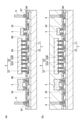
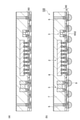
- FIG. 1, FIG. 2, FIG. 3 and FIG. 4 are process diagrams showing an example of a method for manufacturing an electronic component device.
- the methods shown in FIGS. 1 to 4 include a metal wiring 61 and an insulating layer 62, and a plurality of wiring portions 6 having two main surfaces 6S1 and 6S2 facing each other and a plurality of wiring portions 6 provided on one main surface 6S1 of the wiring portion 6.
- a chip component 2 as an electronic component and a chip-type passive component 3 are mounted on the wiring structure 60, and a sealing layer 7 for sealing the electronic component (chip component 2 and the passive component 3) and the conductor pin 5 is provided. It includes forming on the wiring structure 60.
- the wiring structure 60 exemplified in FIG. 1A is prepared in a state of being fixed on the carrier base material 1.
- the carrier base material 1 is a laminate having a support 11 and a temporary fixing material layer 12 provided on the support 11, and a wiring structure 60 is provided on the temporary fixing material layer 12.
- the support 11 may have sufficient strength and rigidity to support electronic components, and its material is not particularly limited.
- the support 11 may be a silicon wafer, a glass plate, or a stainless steel plate.
- the thickness of the support 11 is not particularly limited, but may be, for example, 200 to 2000 ⁇ m.
- the temporary fixing material layer 12 can hold the wiring structure 60 during the mounting of the electronic component and the formation of the sealing layer 7, and has a peelability to the extent that it can be finally peeled off from the wiring structure 60.
- the thickness of the temporary fixing material layer 12 may be, for example, 1 to 100 ⁇ m.
- the material forming the temporary fixing material layer 12 can be selected from the materials used for the purpose of temporary fixing or temporary bonding in the manufacture of the electronic component device (see, for example, International Publication No. 2017/0573555).
- the wiring portion 6 of the wiring structure 60 has a metal wiring 61 and an insulating layer 62 provided between the metal wirings 61.
- the metal wiring 61 includes a multilayer wiring layer 61a extending in a direction parallel to the main surfaces 6S1 and 6S2 of the wiring portion 6 and a connecting portion 61b extending in a direction perpendicular to the main surfaces 6S1 and 6S2 of the wiring portion 6. including.
- the metal wiring 61 constituting the wiring unit 6 includes rewiring connected to the chip component 2 and the passive component 3.
- the thickness of each wiring layer 61a is not particularly limited, but may be, for example, 1 to 30 ⁇ m.
- the thickness of the entire wiring portion 6 may be, for example, 2 to 1000 ⁇ m.
- the wiring portion 6 can be formed by a usual method known to those skilled in the art. For a method of forming a wiring portion including a metal wiring, for example, Japanese Patent No. 5494766 can be referred to.
- the plurality of connection portions provided in the wiring structure 60 include a connection portion 65 connected to the chip component 2, a connection portion 66 connected to the passive component 3, and a connection portion 67 connected to the conductor pin 5. , Each of which is connected to the metal wiring 61.
- the connecting portions 65, 66, 67 may be made of the same metal as the metal wiring 61.
- the connecting portions 65, 66, 67 may include solder bumps.
- the width of the connecting portions 65, 66, 67 may be, for example, 10 to 500 ⁇ m.
- the height of the connecting portions 65, 66, 67 may be, for example, 1 to 25 ⁇ m.
- connection portion 65 in which a plurality of connection portions 67 connected to the conductor pin 5 are connected to electronic components (chip component 2 and passive component 3) mounted on the wiring structure 60 along the outer periphery of the wiring portion 6. It is arranged on one main surface 6S1 of the wiring portion 6 so as to surround 66. In other words, the plurality of connecting portions 67 and the plurality of conductor pins 5 are arranged at intervals from each other so as to form one or more rows surrounding the electronic components.
- the sealing layer 7 fills between two adjacent conductor pins 5 in one row formed by the conductor pins 5.
- the plurality of conductor pins 5 provided on the connection portion 67 arranged in this way can function as an electromagnetic wave shield together with the shield film 8.
- the sealing layer 7 may be completely filled between two adjacent conductor pins 5 in one row formed by the conductor pins 5, but some voids remain to the extent that there is no problem. You may.
- the prepared wiring structure 60 may be inspected.
- the inspection includes, for example, checking for abnormalities due to disconnection or short circuit of the metal wiring 61 and the connection portions 65, 66, 67.
- defective products of the wiring structure 60 can be eliminated before the wiring structure 60 is connected to the electronic components.
- the conductor pin 5 is fixed on the wiring structure 60 while standing with respect to the connection portion 67.
- the columnar conductor pins 5 are fixed on the connecting portion 67 in a direction in which the longitudinal direction of the conductor pins 5 is substantially perpendicular to the main surface 6S1 of the wiring portion 6.
- the conductor pin 5 is fixed on the wiring structure 60 while standing with respect to the connection portion 67 means that the conductor pin 5 has a wiring structure on the surface side of the connection portion 67 opposite to the wiring portion 6. It means that the angle between the longitudinal direction of the conductor pin 5 fixed to the body 60 and the main surface 6S1 of the wiring portion 6 is a right angle or close to a right angle.
- the angle between the longitudinal direction of the fixed conductor pin 5 and the main surface 6S1 of the wiring portion 6 may be, for example, 85 to 95 °.
- One end of the conductor pin 5 is joined to the connecting portion 67 via the solder film 50, whereby the conductor pin 5 is electrically connected to the connecting portion 67.
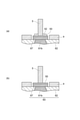
- FIGS. 5 and 6 are process diagrams showing an example of a method of fixing the conductor pin 5 on the wiring structure 60.
- a mask 41 having an opening 41A provided at a position corresponding to the connecting portion 67 is arranged on the main surface 6S1 side where the connecting portion 67 of the wiring portion 6 is provided, and the opening is opened.
- the flux agent 52 is introduced on the connecting portion 67 located inside the 41A, and the opening 42A provided at the position corresponding to the connecting portion 67 on the main surface 6S1 side where the connecting portion 67 of the wiring portion 6 is provided.
- the solder-coated pin 55 having the solder film 50 covering the conductor pin 5 and the surface of the conductor pin 5 is inserted from the opening 42A, whereby the solder-coated pin 55 stands with respect to the connection portion 67.
- the conductor pin 5 is fixed so as to be electrically connected to the connection portion 67 via the solder film 50 by arranging the conductor pin 5 on the connection portion 67 in a state of being in the state of being in the state of being in the state of being in the state of being in the state of being. Includes removing 52.
- a surface insulating layer 4 such as a solder resist may be arranged on the insulating layer 62.
- the flux agent 52 By using the flux agent 52, it is easy to obtain a good connection with the solder film 50.
- the flux agent 52 is not particularly limited and can be arbitrarily selected by those skilled in the art.
- the flux agent 52 is introduced onto the connection portion 67 by, for example, a printing method.
- the conductor pin 5 constituting the solder-coated pin 55 may be a metal molded body having a columnar portion.
- the conductor pin 5 may be a columnar metal molded body containing at least one metal selected from copper, gold, aluminum, silver and the like.
- the maximum width (maximum width of the cross section perpendicular to the longitudinal direction) of the conductor pin 5 (or its columnar portion) may be, for example, 10 to 500 ⁇ m or 50 to 200 ⁇ m.
- the length of the conductor pin 5 (or columnar portion) may be, for example, 50 to 1000 ⁇ m, or 100 to 500 ⁇ m.
- the ratio of the length of the conductor pin 5 (or the columnar portion) to the maximum width of the conductor pin 5 (or the columnar portion) may be 2 to 10.
- the solder film 50 covers the entire or part of the outer surface of the conductor pin 5 (or columnar portion).
- the thickness of the solder film 50 may be, for example, 0.1 to 10 ⁇ m.
- a method comprising sprinkling a large number of solder-coated pins 55 (or conductor pins 5) on the mask 42 and vibrating the wiring structure 60 and the mask 42 in excess of the number of openings 42A, the solder-coated pins 55 (or conductors).
- the pin 5) can be inserted through the opening 42A.
- the minimum width of the opening 42A is usually larger than the maximum width of the solder coated pin 55 (or conductor pin 5).
- the solder film 50 When the solder film 50 is melted by heating the solder coating pin 55 arranged on the connection portion 67 while standing with respect to the connection portion 67, the solder film 50 flows and moves on the connection portion 57.
- the conductor pin 5 is fixed on the wiring structure 60 by the solder film 50 on the connection portion 67, and is electrically connected to the connection portion 67.
- the heating temperature for melting the solder film 50 may be equal to or higher than the melting point of the solder film 50. For example, when the solder film 50 is a Sn—Ag—Cu-based lead-free solder film, the temperature is 250 to 300 ° C. You may.
- the conductor pin 5 After the conductor pin 5 is introduced, electronic components (chip component 2 and passive component 3) are mounted on the wiring structure 60 as shown in FIG. 2 (a).
- the order in which the chip component 2 and the passive component 3 are mounted is arbitrary.
- the conductor pin 5 may be introduced on the wiring structure 60.
- the chip component 2 is electrically connected to the connection portion 65.
- the chip component 2 has an IC chip 21 and a plurality of connection portions 22 provided on the IC chip 21.
- the connecting portion 22 may have a columnar portion 22A containing metal and a bump 22B provided on the columnar portion 22A.
- the maximum width of the chip component 2 in the direction parallel to the main surface 6S1 may be, for example, 0.1 to 50 mm.
- the passive component 3 is electrically connected to the connection portion 66.
- the passive component 3 is selected according to the design of the electronic component device, but may be, for example, a resistor, a capacitor, or a combination thereof.
- the passive component 3 is electrically connected to the connection portion 66 via, for example, the bump 32.
- the maximum width of the passive component 3 in the direction parallel to the main surface 6S1 may be 0.05 to 2 mm, 1 to 2 mm, 0.5 to 1 mm, or 0.1 to 0.5 mm.
- the sealing layer 7 for sealing them is made of a sealing resin material. It is formed.
- the sealing layer 7 is formed so as to embed the entire conductor pin 5 and the electronic component (chip component 2 and passive component 3). When there is a gap between the electronic component and the wiring structure, a part or all of the gap may be filled by the sealing layer 7.
- the sealing layer 7 can be formed in a mold by, for example, a compression or transfer type molding machine.
- the sealing layer 7 may be formed by using a film-shaped sealing resin material (see, for example, International Publication No. 2015/186744). In that case, from the viewpoint of preventing the entrainment of air bubbles, the film-shaped sealing resin material may be laminated under reduced pressure.
- the tip of the conductor pin 5 is exposed as shown in FIG. 3A. Grinding of the sealing layer 7 can be performed using a normal grinding device.
- a conductive shield film 8 covering the surface of the sealing layer 7 opposite to the wiring structure 60 is formed.
- the shield film 8 is connected to the tip of the conductor pin 5.
- the shield film 8 is provided mainly for the purpose of electromagnetic wave shielding.
- the thickness of the shield film 8 may be, for example, 0.1 to 100 ⁇ m.
- the shield film 8 can be a single-layer or multi-layer metal thin film, which can be formed by methods such as sputtering, vapor deposition, or plating.
- the carrier base material 1 is peeled off from the wiring structure 60.
- the carrier base material 1 having the temporary fixing material layer 12 can be peeled off from the wiring portion 6 by, for example, heating, light irradiation, mechanical peeling, or a combination thereof.
- the solder ball 9 connected to the metal wiring 61 is placed on the main surface 6S2 on the side opposite to the sealing layer 7 of the wiring portion 6. May be provided.
- the solder ball 9 is used as a connection terminal for secondary mounting. Reflow is performed if necessary.
- the electronic component device 100 can be obtained by the method exemplified above.
- the electronic component device 100 includes a wiring structure 60, a plurality of electronic components (chip component 2 and passive component 3) mounted on the wiring structure 60, and a sealing layer 7 for sealing the electronic component and the conductor pin 5. It is mainly composed of a conductor pin 5 that penetrates the sealing layer 7 while standing with respect to the connecting portion 67.
- the method for manufacturing the electronic component device is not limited to the example described above, and can be changed as necessary.
- a wiring structure corresponding to a plurality of electronic component devices may be formed on one carrier base material having a large area.
- FIG. 7 is a plan view showing an example of an arrangement of conductor pins in an electronic component device.
- the sealing layer 7 and the shielding film 8 are omitted.
- a plurality of conductor pins 5 are arranged so as to form one or more annular rows.
- the main surface of the wiring portion 6 on the connection portion side is divided into three mounting areas 6A, 6B, and 6C.
- Electronic components are arranged in each mounting area.
- the chip component 2A and the passive component 3 arranged around the chip component 2A are surrounded by two rows L1 and L2 extending along the outer circumference of the mounting area 6A in which they are arranged.
- the row L1 and the row L2 outside the row L1 extend along the outer periphery of the mounting area 6A without intersecting each other, and surround the chip component 2A and the passive component 3.
- the mounting areas 6B and 6C in which the chip components 2B and 2C are arranged are also surrounded by two rows extending along the outer periphery thereof.
- a part of the rows L1 and L2 surrounding the chip component 2A also serves as a row extending along the outer periphery of the mounting areas 6B and 6C in which the chip components 2B and 2C are arranged.
- one or more electronic components are arranged in the mounting area inside one or more rows composed of a plurality of conductor pins.
- the number of rows extending along the outer circumference of one mounting area may be two or more, three or more, or one.
- the distance W between two adjacent conductor pins 5 in the same row may be, for example, 500 ⁇ m or less. Even if the conductor pins 5 are arranged at intervals from each other, if the distance W is small, a sufficient electromagnetic wave shielding effect can be easily obtained even if the conductor material is not provided between the conductor pins 5. From the same viewpoint, the distance W may be 300 ⁇ m or less, 200 ⁇ m or less, or 100 ⁇ m or less. The distance W exceeds 0 ⁇ m from the viewpoint of process stability, reduction of the number of required conductor pins 5, and the like. From the same viewpoint, the distance W may be 50 ⁇ m or more, 75 ⁇ m or more, or 100 ⁇ m or more.
- the distance W'between two adjacent rows may be 100 ⁇ m or more and 500 ⁇ m or less.
- the spacing W' can be the minimum distance between the conductor pins that make up two adjacent rows.
- a plurality of conductor pins 5 are provided in two or more rows (eg, L1, L2) extending along the outer periphery of the mounting area where electronic components are arranged and not intersecting each other. It may be arranged in a staggered arrangement.
- the "staggered arrangement" means that the conductor pins constituting each of the two rows are arranged alternately in the direction in which the two adjacent rows extend.
- the following is an example of a test in which the conductor pin is fixed on the wiring structure while standing with respect to the connection portion.
- a test wiring structure having a connection portion having a circular cross section with a diameter of 200 ⁇ m arranged on the insulating layer was prepared.
- the wiring structure was provided on the insulating layer and had a surface insulating layer having a circular opening surrounding the connection portion.
- a mask 41 metal mask
- a water-soluble flux agent (“WF-6457” manufactured by Senju Metal Industry Co., Ltd.) was printed and the flux agent 52 was introduced on the connection portion 67.
- a mask 42 having a thickness of 145 ⁇ m (including a rib height of 45 ⁇ m) having a circular opening 42A having a diameter of 92 ⁇ m provided at a position corresponding to the connection portion 67 similar to the step shown in FIG. 5 (c).
- Metal mask is installed on the wiring structure 60, and a conductor pin mounting machine (“SBP662” manufactured by Shibuya Kogyo Co., Ltd.) is used to have a conductor pin 5 (copper pin) and a solder coating pin 55 (soldering film 50).
- a mask 42 (diameter 76 ⁇ m, length 180 ⁇ m, manufactured by Finecs Co., Ltd.) through the opening 42A of the mask 42, the mask 42 was placed on the connection portion 67 while standing with respect to the connection portion 67.
- the solder film 50 is melted by reflow under the condition of a maximum temperature of 265 ° C. in a nitrogen atmosphere, and the conductor pin 5 and the connecting portion 57 are connected to the solder film 50.
- the conductor pin 5 was fixed so as to be electrically connected via the wire.
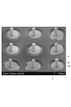
- FIG. 9 is a photomicrograph of the wiring structure and the conductor pins fixed on the wiring structure produced by the above method. As shown in the photograph of FIG. 7, it was confirmed that the conductor pin 5 can be fixed on the wiring structure while standing with respect to the connection portion 67.
Landscapes
- Physics & Mathematics (AREA)
- Production Of Multi-Layered Print Wiring Board (AREA)
- Engineering & Computer Science (AREA)
- Manufacturing & Machinery (AREA)
- Health & Medical Sciences (AREA)
- Electromagnetism (AREA)
- Toxicology (AREA)
- Geometry (AREA)
- Shielding Devices Or Components To Electric Or Magnetic Fields (AREA)
- Electric Connection Of Electric Components To Printed Circuits (AREA)
- Lead Frames For Integrated Circuits (AREA)
Abstract
金属配線及び絶縁層を含み対向する2つの主面を有する配線部と配線部の一方の主面上に設けられた接続部とを有する配線構造体を準備することと、1本以上の導体ピンを、接続部に対して立った状態で配線基板上に固定することと、配線構造体上に1個以上の電子部品を搭載することと、電子部品及び導体ピンを封止する封止層を配線構造体上に形成することとを含む、電子部品装置を製造する方法が開示される。
Description
本開示は、電子部品装置を製造する方法、及び電子部品装置に関する。
各種の半導体パッケージにおいて、半導体チップを封止する封止層を貫通する導電性ビアが設けられることがある(例えば、特許文献1)。封止層を貫通する導電性ビアを形成する従来の方法は、一般に、電解めっきの工程を含む。
本開示の一側面は、電子部品を封止する封止層を貫通する導電ビアを有する電子部品を、より簡易な工程で製造することを可能にする。
本開示の一側面は、金属配線及び絶縁層を含み対向する2つの主面を有する配線部と前記配線部の一方の主面上に設けられた接続部とを有する配線構造体を準備することと、1本以上の導体ピンを、前記接続部に対して立った状態で前記配線構造体上に固定することと、前記配線構造体上に1個以上の電子部品を搭載することと、前記電子部品及び前記導体ピンを封止する封止層を前記配線構造体上に形成することとを含む、電子部品装置を製造する方法を提供する。
本開示の別の一側面は、金属配線及び絶縁層を含み対向する2つの主面を有する配線部と前記配線部の一方の主面上に設けられた接続部とを有する配線構造体と、前記配線構造体に搭載された1個以上の電子部品と、前記電子部品を封止する、前記配線構造体上に形成された封止層と、前記接続部に対して立った状態で前記封止層を貫通する1本以上の導体ピンと、を備える電子部品装置を提供する。
本開示の一側面によれば、封止層を貫通する導電性ビアを有する電子部品装置を、少ない工程で効率的且つ容易に製造することができる。本開示の一側面に係る方法は、幅が狭く、且つある程度の高さを有する導電性ビアを容易に形成できる点でも有利である。
本発明は以下の例に限定されるものではない。
図1、図2、図3及び図4は、電子部品装置を製造する方法の一例を示す工程図である。図1~4に示される方法は、金属配線61及び絶縁層62を含み対向する2つの主面6S1,6S2を有する配線部6と配線部6の一方の主面6S1上に設けられた複数の接続部65,66,67とを有する配線構造体60を準備することと、2本以上の導体ピン5を、接続部67に対して立った状態で配線構造体60上に固定することと、配線構造体60上に電子部品としてのチップ部品2及びチップ型の受動部品3を搭載することと、電子部品(チップ部品2及び受動部品3)及び導体ピン5を封止する封止層7を配線構造体60上に形成することとを含む。
図1の(a)に例示される配線構造体60は、キャリア基材1上に固定された状態で準備される。キャリア基材1は、支持体11、及び支持体11上に設けられた仮固定材層12を有する積層体であり、仮固定材層12上に配線構造体60が設けられる。支持体11は、電子部品を支持可能な程度の強度及び剛性を有していればよく、その材質は特に限定されない。例えば、支持体11が、シリコンウェハ、ガラス板、又はステンレス鋼板であってもよい。支持体11の厚さは、特に制限されないが、例えば200~2000μmであってもよい。仮固定材層12は、電子部品の搭載及び封止層7の形成の間、配線構造体60を保持できるとともに、最終的に配線構造体60から剥離できる程度の剥離性を有する。仮固定材層12の厚さは、例えば1~100μmであってもよい。仮固定材層12を形成する材料は、電子部品装置の製造において、仮固定又は仮接着の目的で用いられている材料から選択することができる(例えば、国際公開第2017/057355号参照)。
配線構造体60の配線部6は、金属配線61と、金属配線61の間に設けられた絶縁層62とを有する。金属配線61は、配線部6の主面6S1,6S2に平行な方向に延在する多層の配線層61aと、配線部6の主面6S1,6S2に垂直な方向に延在する連結部61bとを含む。配線部6を構成する金属配線61は、チップ部品2及び受動部品3に接続される再配線を含む。それぞれの配線層61aの厚さは、特に制限されないが、例えば1~30μmであってもよい。配線部6全体の厚さは、例えば2~1000μmであってもよい。配線部6は、当業者に知られる通常の方法によって形成することができる。金属配線を含む配線部を形成する方法に関しては、例えば、特許第5494766号公報を参照することができる。
配線構造体60に設けられる複数の接続部は、チップ部品2に接続される接続部65と、受動部品3に接続される接続部66と、導体ピン5に接続される接続部67とを含み、それぞれ金属配線61に接続されている。接続部65,66,67は、金属配線61と同様の金属によって形成されていてもよい。接続部65,66,67が、半田バンプを含んでいてもよい。接続部65,66,67の幅は例えば10~500μmであってもよい。接続部65,66,67の高さは例えば1~25μmであってもよい。導体ピン5に接続される複数の接続部67が、配線部6の外周に沿って、配線構造体60に搭載される電子部品(チップ部品2及び受動部品3)に接続される接続部65、66を囲むように配線部6の一方の主面6S1上に配置される。言い換えると、複数の接続部67及び複数の導体ピン5が、電子部品を囲む1本以上の列を形成するように、互いに間隔を空けて配置される。封止層7は、導体ピン5によって形成された1本の列において隣り合う2本の導体ピン5の間を充填する。このように配置された接続部67上に設けられる複数の導体ピン5は、シールド膜8とともに電磁波シールドとして機能することができる。封止層7は、導体ピン5によって形成された1本の列において隣り合う2本の導体ピン5の間を完全に充填していてもよいが、問題がない範囲で一部空隙が残っていてもよい。
準備された配線構造体60を検査してもよい。検査は、例えば金属配線61及び接続部65,66,67の断線又は短絡による異常の有無を確認することを含む。この検査により、配線構造体60に電子部品と接続される前に、配線構造体60の不良品を排除することができる。その結果、封止層内に封止された電子部品上に配線構造体を形成する場合と比較して、正常な電子部品が配線構造体の形成における不具合のために排除される可能性を低くすることができる。
図1の(b)に示されるように、導体ピン5が、接続部67に対して立った状態で配線構造体60上に固定される。言い換えると、柱状の導体ピン5が、導体ピン5の長手方向が配線部6の主面6S1に略垂直な方向に沿う向きで接続部67上に固定される。「導体ピン5が、接続部67に対して立った状態で配線構造体60上に固定される」とは、導体ピン5が、接続部67の配線部6とは反対の面側において配線構造体60に対して固定され、固定された導体ピン5の長手方向と、配線部6の主面6S1との角度が、直角又は直角に近いことを意味する。固定された導体ピン5の長手方向と、配線部6の主面6S1との角度が、例えば85~95°であってもよい。導体ピン5の一端が、半田膜50を介して接続部67に接合され、それにより導体ピン5が接続部67と電気的に接続される。
図5及び図6は、導体ピン5を配線構造体60上に固定する方法の一例を示す工程図である。図5及び図6に示される方法は、配線部6の接続部67が設けられた主面6S1側に、接続部67に対応する位置に設けられた開口41Aを有するマスク41を配置し、開口41Aの内側に位置する接続部67上にフラックス剤52を導入することと、配線部6の接続部67が設けられた主面6S1側に、接続部67に対応する位置に設けられた開口42Aを有するマスク42を配置し、開口42Aから、導体ピン5及び導体ピン5の表面を覆う半田膜50を有する半田被覆ピン55を挿入し、それにより半田被覆ピン55を接続部67に対して立った状態で接続部67上に配置することと、半田膜50を溶融させることによって、導体ピン5を半田膜50を介して接続部67と電気的に接続するように固定することと、フラックス剤52を除去することとを含む。絶縁層62上にソルダーレジストなどの表面絶縁層4を配置してもよい。
フラックス剤52を用いることにより、半田膜50による良好な接続が得られ易い。フラックス剤52は、特に制限されず、当業者が任意に選択することができる。フラックス剤52は、例えば印刷法によって接続部67上に導入される。
半田被覆ピン55を構成する導体ピン5は、柱状部を有する金属成形体であってもよい。導体ピン5は、銅、金、アルミニウム、及び銀等から選ばれる少なくとも1種の金属を含む柱状の金属成形体であってもよい。導体ピン5(又はその柱状部)の最大幅(長手方向に垂直な断面の最大幅)は、例えば10~500μm、又は50~200μmであってもよい。導体ピン5(又は柱状部)の長さは、例えば50~1000μm、又は100~500μmであってもよい。導体ピン5(又は柱状部)の最大幅に対する導体ピン5(又は柱状部)の長さの比が2~10であってもよい。半田膜50は、導体ピン5(又は柱状部)の外表面の全体又は一部を覆っている。半田膜50の厚さは、例えば0.1~10μmであってもよい。
例えば、開口42Aの数を超える多数の半田被覆ピン55(又は導体ピン5)をマスク42上に撒き、配線構造体60及びマスク42を振動させることを含む方法によって、半田被覆ピン55(又は導体ピン5)を開口42Aから挿入することができる。開口42Aの最小幅は、通常、半田被覆ピン55(又は導体ピン5)の最大幅よりも大きい。
接続部67に対して立った状態で接続部67上に配置された半田被覆ピン55を加熱することによって半田膜50を溶融させると、半田膜50が流動して接続部57上に移動する。接続部67上の半田膜50によって、導体ピン5が配線構造体60上に固定されるとともに、接続部67と電気的に接続される。半田膜50を溶融させるための加熱温度は、半田膜50の融点以上であればよく、例えば半田膜50がSn-Ag-Cu系の鉛フリー半田の膜である場合、250~300℃であってもよい。
導体ピン5が導入された後、図2の(a)に示されるように、配線構造体60上に電子部品(チップ部品2及び受動部品3)が搭載される。チップ部品2及び受動部品3を搭載する順番は任意である。チップ部品2及び受動部品3を配線構造体60上に搭載した後、導体ピン5を配線構造体60上に導入してもよい。
チップ部品2は、接続部65と電気的に接続される。チップ部品2は、ICチップ21及びICチップ21上に設けられた複数の接続部22を有する。接続部22は、金属を含む柱状部22A及び柱状部22A上に設けられたバンプ22Bを有していてもよい。チップ部品2の主面6S1に平行な方向における最大幅は、例えば0.1~50mmであってもよい。
受動部品3は、接続部66と電気的に接続される。受動部品3は、電子部品装置の設計に従って選択されるが、例えば、抵抗、コンデンサ又はこれらの組み合わせであってもよい。受動部品3は、例えば、バンプ32を介して接続部66に電気的に接続される。受動部品3の主面6S1に平行な方向における最大幅は、0.05~2mm、1~2mm、0.5~1mm、又は0.1~0.5mmであってもよい。
導体ピン5、チップ部品2及び受動部品3が配線構造体60上に固定された後、図2の(b)に示されるように、これらを封止する封止層7が封止樹脂材によって形成される。封止層7は、導体ピン5、及び電子部品(チップ部品2及び受動部品3)の全体を埋め込むように形成される。電子部品と配線構造体との間に隙間がある場合、その隙間の一部又は全部が封止層7によって充填されてもよい。封止層7は、例えば、コンプレッション又はトランスファー方式の成形機によって、金型内で形成することができる。あるいは、フィルム状の封止樹脂材を用いて封止層7を形成してもよい(例えば、国際公開第2015/186744号参照。)。その場合、気泡の巻き込み防止の観点から、フィルム状の封止樹脂材を減圧下で積層してもよい。
形成された封止層7を配線構造体60とは反対側の面から研削することにより、図3の(a)に示されように、導体ピン5の先端を露出させる。封止層7の研削は、通常の研削装置を用いて行うことができる。
続いて、図3の(b)に示されるように、封止層7の配線構造体60とは反対側の面を覆う導電性のシールド膜8が形成される。シールド膜8は、導体ピン5の先端と接続される。シールド膜8は、主として電磁波シールドの目的で設けられる。シールド膜8の厚さは、例えば0.1~100μmであってもよい。シールド膜8は、単層又は複数層の金属薄膜であることができ、これらは例えばスパッタ、蒸着、又はめっきのような方法によって形成することができる。
図4の(a)に示されるように、キャリア基材1が配線構造体60から剥離される。仮固定材層12を有するキャリア基材1は、例えば、加熱、光照射、機械剥離又はこれらの組み合わせにより、配線部6から剥離することができる。
キャリア基材1の剥離の後、図4の(b)に示されるように、配線部6の封止層7とは反対側の主面6S2上に、金属配線61と接続される半田ボール9を設けてもよい。半田ボール9は二次実装用の接続端子として用いられる。必要によりリフローが行われる。
以上例示された方法によって、電子部品装置100が得られる。電子部品装置100は、配線構造体60と、配線構造体60に搭載された複数の電子部品(チップ部品2及び受動部品3)と、電子部品及び導体ピン5を封止する封止層7と、接続部67に対して立った状態で封止層7を貫通する導体ピン5と、から主として構成される。
電子部品装置を製造する方法は、以上説明した例に限定されるものではなく、必要により変更が可能である。例えば、大面積の1枚のキャリア基材上に、複数の電子部品装置に対応する配線構造体を形成してもよい。
図7は、電子部品装置における導体ピンの配列の一例を示す平面図である。図7において、封止層7及びシールド膜8は省略されている。図7に示される電子部品装置100において、複数の導体ピン5は、1本以上の環状の列を形成するように配置されている。導体ピン5によって形成された列は、配線部6の接続部側の主面を3個の搭載領域6A,6B,6Cに区分している。それぞれの搭載領域内に電子部品が配置されている。例えば、チップ部品2A及びその周囲に配置された受動部品3は、これらが配置された搭載領域6Aの外周に沿って延在する2本の列L1,L2によって囲まれている。列L1及びその外側の列L2は、搭載領域6Aの外周に沿って互いに交差することなく延在するとともに、チップ部品2A及び受動部品3を囲んでいる。チップ部品2B,2Cが配置された搭載領域6B,6Cも、その外周に沿って延在する2本の列によって囲まれている。チップ部品2Aを囲む列L1,L2の一部は、チップ部品2B,2Cが配置される搭載領域6B,6Cの外周に沿って延在する列を兼ねている。
複数の導体ピンによって構成された1本以上の列の内側の搭載領域に、通常、1個以上の電子部品(特にチップ品)が配置される。1個の搭載領域の外周に沿って延在する列の数は、2本以上又は3本以上であってもよく、1本であってもよい。導電ピンによって形成された2本以上の列によって電子部品が囲まれると、より一層高い電磁波シールド効果が得られ易い。
同一の列において隣り合う2本の導体ピン5の間の距離Wは、例えば500μm以下であってもよい。導体ピン5が互いに間隔を空けながら配置されていても、距離Wが小さいと、導体ピン5の間に導体材料が設けられなくても十分な電磁波シールド効果が得られ易い。同様の観点から、距離Wは、300μm以下、200μm以下、又は100μm以下であってもよい。工程の安定性、及び必要とされる導体ピン5の数の低減等の観点から、距離Wは0μmを超える。同様の観点から、距離Wは50μm以上、75μm以上、又は100μm以上であってもよい。
電子部品が配置される搭載領域の外周に沿って2本以上の列が延在する場合、隣り合う2本の列の間の間隔W’は、100μm以上500μm以下であってもよい。間隔W’は、隣り合う2本の列を構成する導体ピンの間の距離の最小値であることができる。
図8に示される別の例のように、電子部品が配置される搭載領域の外周に沿って延在し互いに交差しない2本以上の列(例えばL1,L2)において、複数の導体ピン5が千鳥配列で配置されていてもよい。「千鳥配列」とは、隣り合う2本の列が延在する方向において、2本の列それぞれを構成する導体ピンが互い違いに配置されることを意味する。導体ピン5が千鳥配列に配置されると、より少ない本数の導体ピン5を用いながら、高い電磁波シールド効果を得ることができる。
以下、導体ピンを接続部に対して立った状態で配線構造体上に固定する試験の例を示す。
絶縁層上に配置された直径200μmの円形断面を有する接続部を有する試験用の配線構造体を準備した。配線構造体は、絶縁層上に設けられ、接続部を囲む円形の開口を有する表面絶縁層を有していた。図5の(b)に示される工程と同様に、接続部67に対応する位置に設けられた直径190μmの円形の開口41Aを有する厚さ30μmのマスク41(メタルマスク)を配線構造体上に置き、水溶性フラックス剤(千住金属工業株式会社製「WF-6457」)印刷して、接続部67上にフラックス剤52を導入した。
次に、図5の(c)に示される工程と同様に、接続部67に対応する位置に設けられた直径92μmの円形の開口42Aを有する厚さ145μm(リブ高さ45μm含む)のマスク42(メタルマスク)を配線構造体60上に設置し、導体ピン搭載機(渋谷工業株式会社製「SBP662」)を用いて、導体ピン5(銅ピン)及び半田膜50を有する半田被覆ピン55(直径76μm、長さ180μm、ファインネクス株式会社製)をマスク42の開口42Aから挿入することにより、接続部67に対して立った状態で接続部67上に配置した。
続いて、図6の(a)に示される工程と同様に、窒素雰囲気中、最高温度265℃の条件のリフローにより、半田膜50を溶融させ、導体ピン5と接続部57とが半田膜50を介して電気的に接続されるように導体ピン5を固定した。
最後に、図6の(b)に示される工程と同様に、水洗によりフラックス剤52を除去した。図9は、以上の方法によって作製された、配線構造体及び配線構造体上に固定された導体ピンの顕微鏡写真である。図7の写真に示されるように、導体ピン5を、接続部67に対して立った状態で配線構造体上に固定できることが確認された。
1…キャリア基材、2…チップ部品(電子部品)、3…受動部品(電子部品)、5…導体ピン、6…配線部、6S1,6S2…配線部の主面、7…封止層、8…シールド膜、11…支持体、12…仮固定材層、22,65,66,67…接続部、41,42…マスク、41A,42A…開口、50…半田膜、55…半田被覆ピン、60…配線構造体、61…金属配線、62…絶縁層、100…電子部品装置。
Claims (17)
- 金属配線及び絶縁層を含み対向する2つの主面を有する配線部と前記配線部の一方の主面上に設けられた接続部とを有する配線構造体を準備することと、
1本以上の導体ピンを、前記接続部に対して立った状態で前記配線構造体上に固定することと、
前記配線構造体上に1個以上の電子部品を搭載することと、
前記電子部品及び前記導体ピンを封止する封止層を前記配線構造体上に形成することと、
を含む、電子部品装置を製造する方法。 - 1個以上の前記電子部品が、前記配線部の前記接続部が設けられた主面における1個以上の搭載領域内に配置され、
複数の前記導体ピンが前記配線構造体上に固定され、
複数の前記導体ピンのうち一部又は全部が、1本以上の列を形成するように互いに間隔を空けて配置され、前記搭載領域が、1本以上の前記列によって囲まれた領域であり、
前記封止層が、1本の前記列において隣り合う前記導体ピンの間を充填する、
請求項1に記載の方法。 - 1個以上の前記搭載領域それぞれが、前記搭載領域の外周に沿って延在し互いに交差しない2本以上の前記列によって囲まれる、請求項2に記載の方法。
- 前記搭載領域の外周に沿って延在し互いに交差しない2本以上の前記列が、千鳥配列で配置された複数の前記導体ピンを含む、請求項3に記載の方法。
- 1本の前記列において隣り合う前記導体ピンの間の距離が、50μmを超え250μm以下である、請求項2~4のいずれか一項に記載の方法。
- 当該方法が、前記封止層を覆い、前記導体ピンの先端と接続された導電性のシールド膜を形成することを更に含む、請求項1~5のいずれか一項に記載の方法。
- 当該方法が、前記封止層を前記配線構造体とは反対側の面から研削することにより、前記導体ピンの先端を露出させることを更に含む、請求項1~6のいずれか一項に記載の方法。
- 前記配線構造体の前記接続部が設けられた主面側に、開口を有するマスクを配置し、前記開口から前記導体ピンを挿入することを含む方法によって、前記導体ピンが前記接続部に対して立った状態で前記配線構造体上に固定される、請求項1~7のいずれか一項に記載の方法。
- 前記導体ピンが柱状部を有し、前記導体ピンと前記導体ピンの前記柱状部の外表面を覆う半田膜とを有する半田被覆ピンを前記接続部に対して立った状態で配置し、その状態で前記半田膜を溶融させることによって、前記導体ピンが、前記接続部と半田を介して電気的に接続するように前記配線構造体上に固定される、請求項1~8のいずれか一項に記載の方法。
- 前記導体ピンが、最大幅10~500μm、長さ50~1000μmの柱状部を有する金属成形体である、請求項1~9のいずれか一項に記載の方法。
- 金属配線及び絶縁層を含み対向する2つの主面を有する配線部と前記配線部の一方の主面上に設けられた接続部とを有する配線構造体と、
前記配線構造体に搭載された1個以上の電子部品と、
前記電子部品を封止する、前記配線構造体上に形成された封止層と、
前記接続部に対して立った状態で前記封止層を貫通する1本以上の導体ピンと、
を備える電子部品装置。 - 1個以上の前記電子部品が、前記配線部の前記接続部が設けられた主面における1個以上の搭載領域内に配置され、
当該電子部品装置が複数の前記導体ピンを備え、
複数の前記導体ピンのうち一部又は全部が、1本以上の列を形成するように互いに間隔を空けて配置され、前記搭載領域が、1本以上の前記列によって囲まれた領域であり、
前記封止層が、1本の前記列において隣り合う前記導体ピンの間を充填する、
請求項11に記載の電子部品装置。 - 1個以上の前記搭載領域それぞれが、前記搭載領域の外周に沿って延在し互いに交差しない2本以上の前記列によって囲まれる、請求項12に記載の電子部品装置。
- 前記搭載領域の外周に沿って延在し互いに交差しない2本以上の前記列が、千鳥配列で配置された複数の前記導体ピンを含む、請求項13に記載の電子部品装置。
- 1本の前記列において隣り合う前記導体ピンの間の距離が、50μmを超え250μm以下である、請求項12~14のいずれか一項に記載の電子部品装置。
- 当該電子部品装置が、前記封止層を覆い、前記導体ピンの先端と接続された導電性のシールド膜を更に備える、請求項11~15のいずれか一項に記載の電子部品装置。
- 前記導体ピンと前記接続部との間に介在する半田膜を更に有する、請求項11~16のいずれか一項に記載の電子部品装置。
Priority Applications (2)
| Application Number | Priority Date | Filing Date | Title |
|---|---|---|---|
| JP2022546330A JP7750242B2 (ja) | 2020-09-02 | 2021-08-31 | 電子部品装置を製造する方法、及び電子部品装置 |
| US18/043,582 US12628660B2 (en) | 2020-09-02 | 2021-08-31 | Method for manufacturing electronic component device and electronic component device |
Applications Claiming Priority (2)
| Application Number | Priority Date | Filing Date | Title |
|---|---|---|---|
| PCT/JP2020/033259 WO2022049671A1 (ja) | 2020-09-02 | 2020-09-02 | 電子部品装置を製造する方法、及び電子部品装置 |
| JPPCT/JP2020/033259 | 2020-09-02 |
Publications (1)
| Publication Number | Publication Date |
|---|---|
| WO2022050256A1 true WO2022050256A1 (ja) | 2022-03-10 |
Family
ID=80490984
Family Applications (2)
| Application Number | Title | Priority Date | Filing Date |
|---|---|---|---|
| PCT/JP2020/033259 Ceased WO2022049671A1 (ja) | 2020-09-02 | 2020-09-02 | 電子部品装置を製造する方法、及び電子部品装置 |
| PCT/JP2021/031877 Ceased WO2022050256A1 (ja) | 2020-09-02 | 2021-08-31 | 電子部品装置を製造する方法、及び電子部品装置 |
Family Applications Before (1)
| Application Number | Title | Priority Date | Filing Date |
|---|---|---|---|
| PCT/JP2020/033259 Ceased WO2022049671A1 (ja) | 2020-09-02 | 2020-09-02 | 電子部品装置を製造する方法、及び電子部品装置 |
Country Status (3)
| Country | Link |
|---|---|
| US (1) | US12628660B2 (ja) |
| JP (1) | JP7750242B2 (ja) |
| WO (2) | WO2022049671A1 (ja) |
Citations (2)
| Publication number | Priority date | Publication date | Assignee | Title |
|---|---|---|---|---|
| WO2016181954A1 (ja) * | 2015-05-11 | 2016-11-17 | 株式会社村田製作所 | 高周波モジュール |
| JP2019068020A (ja) * | 2017-10-05 | 2019-04-25 | 千住金属工業株式会社 | 核カラムの実装方法 |
Family Cites Families (20)
| Publication number | Priority date | Publication date | Assignee | Title |
|---|---|---|---|---|
| JP3821630B2 (ja) | 2000-03-31 | 2006-09-13 | 株式会社東芝 | 高周波シールド構造 |
| JP3757941B2 (ja) * | 2003-01-21 | 2006-03-22 | 日本電気株式会社 | ピン取付治具、ピン取付方法及び半導体装置の実装構造 |
| KR101049389B1 (ko) | 2005-12-16 | 2011-07-14 | 이비덴 가부시키가이샤 | 다층 프린트 배선판 및 그 제조 방법 |
| CN101653053B (zh) | 2008-01-25 | 2012-04-04 | 揖斐电株式会社 | 多层线路板及其制造方法 |
| US7709915B2 (en) * | 2008-05-07 | 2010-05-04 | Aptina Imaging Corporation | Microelectronic devices having an EMI shield and associated systems and methods |
| KR101398754B1 (ko) | 2008-12-26 | 2014-05-27 | 히타치가세이가부시끼가이샤 | 포지티브형 감광성 수지 조성물, 레지스트 패턴의 제조 방법, 반도체 장치 및 전자 디바이스 |
| JP2011003651A (ja) * | 2009-06-17 | 2011-01-06 | Fujitsu Ten Ltd | 回路装置、及び電子機器 |
| JP2012019091A (ja) * | 2010-07-08 | 2012-01-26 | Sony Corp | モジュールおよび携帯端末 |
| US9818734B2 (en) * | 2012-09-14 | 2017-11-14 | STATS ChipPAC Pte. Ltd. | Semiconductor device and method of forming build-up interconnect structures over a temporary substrate |
| JP5422830B2 (ja) * | 2012-09-27 | 2014-02-19 | 新光電気工業株式会社 | リードピン付配線基板及びその製造方法 |
| US9048222B2 (en) | 2013-03-06 | 2015-06-02 | Taiwan Semiconductor Manufacturing Company, Ltd. | Method of fabricating interconnect structure for package-on-package devices |
| JP5466785B1 (ja) * | 2013-08-12 | 2014-04-09 | 太陽誘電株式会社 | 回路モジュール及びその製造方法 |
| WO2015186744A1 (ja) | 2014-06-04 | 2015-12-10 | 日立化成株式会社 | フィルム状エポキシ樹脂組成物、フィルム状エポキシ樹脂組成物の製造方法、及び半導体装置の製造方法 |
| TWI671831B (zh) | 2015-09-30 | 2019-09-11 | 日商富士軟片股份有限公司 | 半導體元件的製造方法 |
| WO2017094836A1 (ja) * | 2015-12-04 | 2017-06-08 | 株式会社村田製作所 | シールドを有するモジュール |
| WO2018101381A1 (ja) * | 2016-12-02 | 2018-06-07 | 株式会社村田製作所 | 高周波モジュール |
| US10177095B2 (en) | 2017-03-24 | 2019-01-08 | Amkor Technology, Inc. | Semiconductor device and method of manufacturing thereof |
| JP2020113559A (ja) | 2017-03-30 | 2020-07-27 | 株式会社村田製作所 | 回路モジュール |
| US10157888B1 (en) * | 2017-06-20 | 2018-12-18 | Taiwan Semiconductor Manufacturing Co., Ltd. | Integrated fan-out packages and methods of forming the same |
| US11410918B2 (en) * | 2017-11-15 | 2022-08-09 | Taiwan Semiconductor Manufacturing Company, Ltd. | Method of making an integrated circuit package including an integrated circuit die soldered to a bond pad of a carrier |
-
2020
- 2020-09-02 WO PCT/JP2020/033259 patent/WO2022049671A1/ja not_active Ceased
-
2021
- 2021-08-31 US US18/043,582 patent/US12628660B2/en active Active
- 2021-08-31 JP JP2022546330A patent/JP7750242B2/ja active Active
- 2021-08-31 WO PCT/JP2021/031877 patent/WO2022050256A1/ja not_active Ceased
Patent Citations (2)
| Publication number | Priority date | Publication date | Assignee | Title |
|---|---|---|---|---|
| WO2016181954A1 (ja) * | 2015-05-11 | 2016-11-17 | 株式会社村田製作所 | 高周波モジュール |
| JP2019068020A (ja) * | 2017-10-05 | 2019-04-25 | 千住金属工業株式会社 | 核カラムの実装方法 |
Also Published As
| Publication number | Publication date |
|---|---|
| US20230268195A1 (en) | 2023-08-24 |
| WO2022049671A1 (ja) | 2022-03-10 |
| JP7750242B2 (ja) | 2025-10-07 |
| JPWO2022050256A1 (ja) | 2022-03-10 |
| US12628660B2 (en) | 2026-05-12 |
Similar Documents
| Publication | Publication Date | Title |
|---|---|---|
| JP6081044B2 (ja) | パッケージ基板ユニットの製造方法 | |
| TWI496259B (zh) | 封裝裝置及其製造方法 | |
| US8324740B2 (en) | Semiconductor device, and method of manufacturing multilayer wiring board and semiconductor device | |
| KR100702018B1 (ko) | 반도체 장치의 제조 방법 및 반도체 장치 | |
| US9899304B2 (en) | Wiring substrate and semiconductor device | |
| US10283434B2 (en) | Electronic device, method for manufacturing the electronic device, and electronic apparatus | |
| US9949372B2 (en) | Printed wiring board and method for manufacturing the same | |
| US11302647B2 (en) | Semiconductor device package including conductive layers as shielding and method of manufacturing the same | |
| US10856415B2 (en) | Printed wiring board and method for manufacturing the same | |
| JPH1167968A (ja) | ボールグリッドアレーパッケージ用印刷回路基板及びボールグリッドアレーパッケージ並びにそれらの製造方法 | |
| US10134665B2 (en) | Semiconductor device | |
| US10304767B2 (en) | Semiconductor device | |
| JP2001015650A (ja) | ボールグリッドアレイパッケージとその製造方法 | |
| KR20220144107A (ko) | 반도체 패키지 및 그 제조 방법 | |
| CN111696950A (zh) | 具有部分凹进电容器的封装衬底 | |
| KR102380834B1 (ko) | 인쇄회로기판, 반도체 패키지 및 이들의 제조방법 | |
| KR20250079113A (ko) | 반도체 장치 및 이의 제조 방법 | |
| US20090184413A1 (en) | Insulative wiring board, semiconductor package using the same, and method for producing the insulative wiring board | |
| US11212912B1 (en) | Printed circuit board mesh routing to reduce solder ball joint failure during reflow | |
| CN104779236B (zh) | 用于ic封装基板的倒装芯片焊盘几何结构 | |
| US20100102457A1 (en) | Hybrid Semiconductor Chip Package | |
| US12628660B2 (en) | Method for manufacturing electronic component device and electronic component device | |
| JP3522403B2 (ja) | 半導体装置 | |
| US11749596B2 (en) | Wiring substrate | |
| CN114203691B (zh) | 一种多芯片高密度互连封装结构及其制作方法 |
Legal Events
| Date | Code | Title | Description |
|---|---|---|---|
| 121 | Ep: the epo has been informed by wipo that ep was designated in this application |
Ref document number: 21864314 Country of ref document: EP Kind code of ref document: A1 |
|
| ENP | Entry into the national phase |
Ref document number: 2022546330 Country of ref document: JP Kind code of ref document: A |
|
| NENP | Non-entry into the national phase |
Ref country code: DE |
|
| 122 | Ep: pct application non-entry in european phase |
Ref document number: 21864314 Country of ref document: EP Kind code of ref document: A1 |