WO2022045140A1 - セラミック板及びその製造方法、接合基板及びその製造方法、並びに、回路基板及びその製造方法 - Google Patents
セラミック板及びその製造方法、接合基板及びその製造方法、並びに、回路基板及びその製造方法 Download PDFInfo
- Publication number
- WO2022045140A1 WO2022045140A1 PCT/JP2021/031003 JP2021031003W WO2022045140A1 WO 2022045140 A1 WO2022045140 A1 WO 2022045140A1 JP 2021031003 W JP2021031003 W JP 2021031003W WO 2022045140 A1 WO2022045140 A1 WO 2022045140A1
- Authority
- WO
- WIPO (PCT)
- Prior art keywords
- ceramic plate
- ceramic
- plate
- cut
- main surface
- Prior art date
- Legal status (The legal status is an assumption and is not a legal conclusion. Google has not performed a legal analysis and makes no representation as to the accuracy of the status listed.)
- Ceased
Links
Images


Classifications
-
- B—PERFORMING OPERATIONS; TRANSPORTING
- B23—MACHINE TOOLS; METAL-WORKING NOT OTHERWISE PROVIDED FOR
- B23K—SOLDERING OR UNSOLDERING; WELDING; CLADDING OR PLATING BY SOLDERING OR WELDING; CUTTING BY APPLYING HEAT LOCALLY, e.g. FLAME CUTTING; WORKING BY LASER BEAM
- B23K26/00—Working by laser beam, e.g. welding, cutting or boring
- B23K26/36—Removing material
- B23K26/38—Removing material by boring or cutting
-
- B—PERFORMING OPERATIONS; TRANSPORTING
- B28—WORKING CEMENT, CLAY, OR STONE
- B28B—SHAPING CLAY OR OTHER CERAMIC COMPOSITIONS; SHAPING SLAG; SHAPING MIXTURES CONTAINING CEMENTITIOUS MATERIAL, e.g. PLASTER
- B28B11/00—Apparatus or processes for treating or working the shaped or preshaped articles
- B28B11/12—Apparatus or processes for treating or working the shaped or preshaped articles for removing parts of the articles by cutting
-
- C—CHEMISTRY; METALLURGY
- C04—CEMENTS; CONCRETE; ARTIFICIAL STONE; CERAMICS; REFRACTORIES
- C04B—LIME, MAGNESIA; SLAG; CEMENTS; COMPOSITIONS THEREOF, e.g. MORTARS, CONCRETE OR LIKE BUILDING MATERIALS; ARTIFICIAL STONE; CERAMICS; REFRACTORIES; TREATMENT OF NATURAL STONE
- C04B37/00—Joining burned ceramic articles with other burned ceramic articles or other articles by heating
- C04B37/02—Joining burned ceramic articles with other burned ceramic articles or other articles by heating with metallic articles
-
- C—CHEMISTRY; METALLURGY
- C04—CEMENTS; CONCRETE; ARTIFICIAL STONE; CERAMICS; REFRACTORIES
- C04B—LIME, MAGNESIA; SLAG; CEMENTS; COMPOSITIONS THEREOF, e.g. MORTARS, CONCRETE OR LIKE BUILDING MATERIALS; ARTIFICIAL STONE; CERAMICS; REFRACTORIES; TREATMENT OF NATURAL STONE
- C04B41/00—After-treatment of mortars, concrete, artificial stone or ceramics; Treatment of natural stone
- C04B41/80—After-treatment of mortars, concrete, artificial stone or ceramics; Treatment of natural stone of only ceramics
- C04B41/91—After-treatment of mortars, concrete, artificial stone or ceramics; Treatment of natural stone of only ceramics involving the removal of part of the materials of the treated articles, e.g. etching
-
- H—ELECTRICITY
- H05—ELECTRIC TECHNIQUES NOT OTHERWISE PROVIDED FOR
- H05K—PRINTED CIRCUITS; CASINGS OR CONSTRUCTIONAL DETAILS OF ELECTRIC APPARATUS; MANUFACTURE OF ASSEMBLAGES OF ELECTRICAL COMPONENTS
- H05K1/00—Printed circuits
- H05K1/02—Details
-
- H—ELECTRICITY
- H05—ELECTRIC TECHNIQUES NOT OTHERWISE PROVIDED FOR
- H05K—PRINTED CIRCUITS; CASINGS OR CONSTRUCTIONAL DETAILS OF ELECTRIC APPARATUS; MANUFACTURE OF ASSEMBLAGES OF ELECTRICAL COMPONENTS
- H05K3/00—Apparatus or processes for manufacturing printed circuits
Definitions
- This disclosure relates to a ceramic plate and its manufacturing method, a bonded substrate and its manufacturing method, and a circuit board and its manufacturing method.
- Insulating ceramic plates may be used for circuit boards mounted on electronic devices and the like.
- a technique for manufacturing such a circuit board a technique is known in which a metal plate is joined to the main surface of a ceramic plate to form a bonded board, and a circuit pattern is formed from the metal plate of the joined board to manufacture the circuit board. ..
- the ceramic plate used for such a circuit board is provided with a margin portion at an end in order to process it into a predetermined size.
- the margin portion is removed by folding along the break line formed by the laser beam.
- the alignment of the ceramic plates is high when joining a metal plate to a ceramic plate or forming a conductor part at a predetermined position. It is necessary to do it accurately.
- the ceramic plate stress remains inside due to the heat history associated with firing. There is a concern that this stress will cause warpage and make accurate alignment difficult.
- the present disclosure provides a ceramic plate capable of positioning with high accuracy and a method for manufacturing the same. Further, by having such a ceramic plate, a bonded substrate having excellent dimensional accuracy and a manufacturing method thereof, and a circuit board and a manufacturing method thereof are provided.
- the present disclosure provides a ceramic plate having a corner portion, wherein the corner portion and the side surface adjacent to each other via the corner portion are formed of a cut surface cut by a laser beam.
- the cut surface cut by the laser beam can suppress the occurrence of chipping and burrs as compared with the fracture surface generated by folding. Therefore, the accuracy of positioning using the corners can be improved.
- the thermal shock of the laser beam causes fine microcracks that do not interfere with the positioning along the thickness direction of the ceramic plate.
- the presence of such microcracks on the corners and sides formed by the cut surface can relieve the stress of the ceramic plate. That is, the microcracks are deformed to close in the portion where the tensile stress is generated, and the microcracks are deformed to open in the portion where the compressive stress is generated. In this way, stress is relieved and warpage at the corners between adjacent sides is suppressed.
- the above-mentioned ceramic plate can suppress warpage while suppressing the occurrence of chipping and burrs at the corners. Therefore, it is possible to perform positioning with high accuracy using the corners.
- the present disclosure provides a ceramic plate composed of a cut surface whose entire side surface is cut by a laser beam.
- the cut surface cut by the laser beam can suppress the occurrence of chipping and burrs as compared with the fracture surface generated by folding. Therefore, it is possible to perform positioning with high accuracy by using the peripheral portion of the main surface.
- the thermal shock of the laser beam causes fine microcracks that do not interfere with the positioning along the thickness direction of the ceramic plate.
- the presence of such microcracks on the side surface composed of the cut surface can release the stress of the ceramic plate. That is, the microcracks are deformed to close in the portion where the tensile stress is generated, and the microcracks are deformed to open in the portion where the compressive stress is generated. In this way, the stress is relaxed and the warpage near the side surface is suppressed.
- the above-mentioned ceramic plate can suppress the occurrence of chipping and burrs on the side surface and also the warp, it can be positioned with high accuracy by using the peripheral portion of the main surface.
- the above-mentioned ceramic plate includes a plurality of compartments formed by a scribe line formed on the main surface, and an outer edge portion surrounding the plurality of compartments and including a side surface, and the area occupied by the outer edge portion on the main surface.
- the ratio may be 8% or less.
- the present disclosure provides a bonded substrate comprising a ceramic plate and a metal plate bonded to the ceramic plate. Since this bonding substrate includes the above-mentioned ceramic plate, the alignment accuracy between the ceramic plate and the metal plate can be improved. Therefore, the position accuracy of the ceramic plate and the metal plate is excellent. Therefore, the positional deviation between the ceramic plate and the metal plate is sufficiently reduced, and the dimensional accuracy is excellent.
- the present disclosure provides a circuit board comprising the above-mentioned ceramic plate and a plurality of conductor portions joined to the ceramic plate. Since this circuit board includes the above-mentioned ceramic plate, the position accuracy of the ceramic plate and the conductor portion is excellent. That is, the misalignment of the conductor portion on the main surface of the ceramic plate is sufficiently reduced, and the dimensional accuracy is excellent.
- the present disclosure comprises a step of irradiating a main surface of a plate-shaped ceramic substrate with a laser beam to cut an end portion of the ceramic substrate to form a corner portion and adjacent side surfaces via the corner portion.
- a method for manufacturing a plate is provided. In this manufacturing method, a corner portion and adjacent side surfaces are formed via the corner portion by laser light. Therefore, the corner portion and the side surface thereof are composed of a cut surface. Such a cut surface can suppress the occurrence of chipping and burrs as compared with the fracture surface generated by folding. Therefore, the accuracy of positioning using the corner portion can be improved.
- the thermal shock of the laser beam causes fine microcracks that do not interfere with positioning along the thickness direction of the ceramic plate. Occurs.
- the presence of such microcracks on the corners and sides formed by the cut surface can relieve the stress of the ceramic plate. That is, the microcracks are deformed to close in the portion where the tensile stress is generated, and the microcracks are deformed to open in the portion where the compressive stress is generated. In this way, stress is relieved and warpage at the corners between adjacent sides is suppressed.
- the ceramic plate obtained by the above-mentioned manufacturing method can suppress the occurrence of chipping and burrs at the corners and also suppress the warp, so that the ceramic plate can be positioned with high accuracy by using the corners.
- the present disclosure comprises a step of joining a ceramic plate manufactured by any of the above-mentioned manufacturing methods and a metal plate to prepare a bonded substrate, and positioning the corner portion when joining the ceramic plate and the metal plate.
- a method for manufacturing a bonded substrate used in the above Since the ceramic plate obtained by the above-mentioned manufacturing method is used for this bonding substrate, the alignment accuracy between the ceramic plate and the metal plate can be improved. Therefore, it is possible to manufacture a bonded substrate having excellent positional accuracy between the ceramic plate and the metal plate. Since the positional deviation between the ceramic plate and the metal plate is sufficiently reduced in this way, it is possible to manufacture a bonded substrate having excellent dimensional accuracy.
- the present disclosure provides a method for manufacturing a circuit board, which comprises a step of removing a part of a metal plate in the bonded board manufactured by the above-mentioned manufacturing method to form a conductor portion. Since this manufacturing method uses the bonded substrate obtained by the above-mentioned manufacturing method, it is possible to manufacture a circuit board having excellent positional accuracy between the ceramic plate and the conductor portion. That is, the misalignment of the conductor portion on the main surface of the ceramic plate is sufficiently reduced, and a circuit board having excellent dimensional accuracy can be manufactured.
- a ceramic plate capable of positioning with high accuracy and a method for manufacturing the same. Further, by having such a ceramic plate, it is possible to provide a bonded substrate having excellent dimensional accuracy and a method for manufacturing the same, and a circuit board and a method for manufacturing the same.
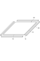
- FIG. 5 is a sectional view taken along line IV-IV of FIG. It is a perspective view which shows an example of the ceramic plate coated with the brazing material. It is a perspective view which conceptually shows the alignment of a ceramic plate and a metal plate. It is a perspective view of the bonded substrate which concerns on one Embodiment. It is a perspective view which shows an example of the bonded substrate in which the resist pattern was formed on the main surface. It is a perspective view of the circuit board which concerns on one Embodiment.
- the main surface 60A of the plate-shaped ceramic base material 60 shown in FIG. 1 is irradiated with laser light to cut the end portion of the ceramic base material 60, and the corner portion and the corner portion are cut. It has a step of forming adjacent side surfaces via a portion.
- Examples of the laser light include a carbon dioxide gas laser and a YAG laser.
- the main surface 60A can be irradiated with laser light to form a plurality of holes so as to be continuous with each other, and the end portion of the ceramic base material 60 can be cut.
- the irradiation of the laser beam is performed along the cutting line C1.
- a hole may be formed by repeatedly irradiating the main surface 60A with a laser beam a plurality of times, or a hole may be formed by irradiating only once. When the holes are formed by repeating the process a plurality of times, the energy of the laser beam irradiated at each time can be reduced.
- the width of the end portion 62 to be cut off (the cutting width of the ceramic base material 60), that is, the width of the cutting line C1 may be 10 times or less than the thickness of the ceramic plate 101, and may be 8 times or less. By reducing the cutting width of the ceramic base material 60 in this way, the ceramic base material 60 can be effectively used.
- the ceramic plate 101 obtained in the above step has a quadrangular prism shape, but the ceramic plate is not limited to such a shape.
- the number of times the laser light irradiation is repeated is not particularly limited, and may be, for example, 2 to 5 times.
- the irradiation conditions may be the same or different each time. Further, the repeated irradiation of the laser beam may be performed at exactly the same position, or may be performed at different positions.
- the output of the laser light may be 50 to 250 W.
- the output is less than 50 W, the number of repeated irradiations increases, and the time required for cutting the ceramic substrate tends to increase.
- the output exceeds 250 W, the amount of fumes and dross generated when cutting the ceramic substrate tends to increase.
- the scanning speed of the laser beam may be 20 to 300 mm / min. If the scanning speed is less than 20 mm / min, heat due to irradiation with laser light is accumulated, and the amount of fumes and dross tends to increase. When the scanning speed exceeds 300 mm / min, the number of repetitions of laser light irradiation increases, and the time required for cutting the ceramic substrate tends to increase.
- the frequency of the laser beam may be 0.5 to 500 kHz.
- the frequency is less than 0.5 kHzn, the amount of energy per pulse tends to increase, and the amount of fumes and dross tends to increase.
- the frequency exceeds 500 kHz, the number of repetitions of laser light irradiation increases, and the time required for cutting the ceramic substrate tends to increase.
- Cutting by laser light may be performed by the burst pulse mode or the cycle pulse mode.
- the burst pulse mode is performed by the following procedure.
- the laser beam is applied to the same position in multiple times to form the first hole.
- the laser beam is irradiated in a plurality of times so as to be adjacent to the first hole to form the second hole. This forms two holes adjacent to each other.
- Such a procedure is repeated a plurality of times to form n holes (n is a positive integer of 2 or more). In this way, the ceramic base material 60 can be cut and the end portion 62 can be separated.
- the first to nth holes are formed by irradiating each laser beam once. After that, the first to nth holes are irradiated with the laser beam once again. In this case, the laser beam is irradiated in 2n times in order to form n holes.
- the number of times of irradiating the laser beam before each hole penetrates may be three or more.
- the method of forming a hole is not limited to the above two methods. For example, a burst pulse mode and a cycle pulse mode may be combined.
- the irradiation interval of the multiple laser beams irradiated to form one hole is 1200 ⁇ sec or more (850 Hz or less) in order to secure the cooling time of the ceramic plate 101 obtained by cutting by the laser beam irradiation. It may be 1500 ⁇ sec or more (670 Hz or less).
- the energy of the laser beam irradiated at one time may be less than 70 mJ, may be 50 mJ or less, and may be 30 mJ or less. By reducing the energy irradiated each time in this way, it is possible to reduce the amount of foreign matter generated on the corners and side surfaces. From the viewpoint of efficiently forming holes, the energy of the laser beam irradiated at one time may be 5 mJ or more, and may be 10 mJ or more.
- the pulse width of the laser beam is 30 to 200 ⁇ sec from the viewpoint of forming a hole sufficiently large in the main surface 60A of the ceramic base material 60 and reducing damage to the ceramic plate 101 obtained by cutting. It may be 50 to 150 ⁇ sec.
- the ceramic base material 60 used in each of the above-described embodiments can be manufactured, for example, by the following procedure. First, a slurry containing a ceramic powder, a binder resin, a sintering aid, a plasticizer, a dispersant, a solvent and the like is molded to obtain a green sheet.
- the ceramic powder include aluminum nitride powder, silicon nitride powder, and aluminum oxide powder.
- the sintering aid include rare earth metals, alkaline earth metals, metal oxides, fluorides, chlorides, nitrates, sulfates and the like. These may be used alone or in combination of two or more. By using the sintering aid, the sintering of the ceramic powder can be promoted.
- the binder resin include methyl cellulose, ethyl cellulose, polyvinyl alcohol, polyvinyl butyral, and (meth) acrylic resins.
- plasticizer examples include phthalic acid-based plasticizers such as purified glycerin, glycerin triolate, diethylene glycol, and di-n-butylphthalate, and dibasic acid-based plasticizers such as di-2-ethylhexyl sebacate.
- dispersants include poly (meth) acrylic acid salts and (meth) acrylic acid-maleate copolymers.
- solvent examples include organic solvents such as ethanol and toluene.
- Examples of the slurry molding method include a doctor blade method and an extrusion molding method.
- a green sheet is produced by such a method.
- the ceramic base material 60 is obtained by degreasing and sintering the green sheet.
- Solvent degreasing may be carried out by heating at, for example, 400 to 800 ° C. for 0.5 to 20 hours. This makes it possible to reduce the residual amount of the organic substance (carbon) while suppressing the oxidation and deterioration of the ceramic base material 60.
- Firing may be carried out by heating to 1700 to 1900 ° C. in a non-oxidizing gas atmosphere such as nitrogen, argon, ammonia or hydrogen.
- the above-mentioned degreasing and sintering may be performed in a state where a plurality of green sheets are laminated.
- a mold release layer with a mold release agent may be provided between the green sheets in order to facilitate separation of the base material after firing.
- the mold release agent for example, boron nitride (BN) can be used.
- the release layer may be formed by applying, for example, a slurry of boron nitride powder by a method such as spraying, brushing, roll coating, or screen printing.
- the number of green sheets to be laminated may be, for example, 8 to 50 sheets or 10 to 50 sheets from the viewpoint of sufficiently advancing degreasing while efficiently mass-producing the ceramic base material.
- FIG. 3 is a side view of the ceramic plate 101.
- the thermal stress becomes large, as shown by the dotted line E in FIG. 3, the outer edge portion of the ceramic plate 101 tends to be warped. If such a warp becomes large, the position of the corner portion 12 may shift, which causes a decrease in the alignment accuracy.
- the end portion When the end portion is cut with a laser beam, fine microcracks are generated on the corner portion 12 and the side surface 10 of the ceramic plate 101 due to the thermal shock of the laser beam. Since the laser beam is emitted from the main surface 60A of the ceramic base material 60 along the thickness direction of the ceramic base material 60, the microcracks are formed so as to extend in the thickness direction at the corner portion 12 and the side surface 10.
- the stress of the ceramic plate 101 can be released by the presence of microcracks extending along the thickness direction of the ceramic plate 101 on the corner portion 12 and the side surface 10. That is, the microcracks are deformed to close in the portion where the tensile stress is generated, and the microcracks are deformed to open in the portion where the compressive stress is generated. In this way, the occurrence of warpage at the corners 12 between the adjacent side surfaces 10 is suppressed. As described above, since the ceramic plate 101 suppresses the occurrence of chipping and burrs at the corners 12 and also suppresses the occurrence of warpage, the ceramic plate 101 is positioned with high accuracy by using the corners 12. be able to.
- the entire four corners 12 and the four side surfaces 10 of the ceramic plate 101 having a square pillar shape are composed of cut surfaces. That is, the ceramic plate 101 does not have a fracture surface on the corner portion 12 and the side surface 10, and is composed only of a cut surface. Therefore, burrs and chips can be sufficiently reduced.
- the microcracks generated on the cut surface are much smaller than such burrs and chips, and have a size that does not affect positioning.
- FIG. 4 is a perspective view for explaining a method for manufacturing a ceramic plate according to still another embodiment.
- the ceramic base material 60 is hollowed out and the end portion 64 is cut off to manufacture the ceramic plate 102.
- the end portion of the flat plate-shaped ceramic base material 60 is cut with a laser beam to form a ceramic plate 102 having a corner portion 12 formed of a cut surface and side surfaces 10 adjacent to each other via the corner portion 12.
- the ceramic plate 102 can also be positioned with high accuracy by using the corner portions 12.
- FIG. 5 is a perspective view of the ceramic plate according to the embodiment.
- the ceramic plate 100 of FIG. 5 has a flat plate shape.
- the main surface 100A of the ceramic plate 100 is divided into a plurality of parts by a scribe line.
- a plurality of scribe lines L1 extending along the first direction and arranging at equal intervals and scribe lines L1 extending along the second direction orthogonal to the first direction and arranging at equal intervals are arranged.
- a plurality of scribe lines L2 and are provided.
- the scribe line L1 and the scribe line L2 are orthogonal to each other.
- a plurality of holes are formed side by side along the first direction.
- a plurality of holes are formed side by side along a second direction. Adjacent holes may be separated or connected. Part of the adjacent holes may overlap each other.
- the inner portion of the scribe lines L1 and L2 provided closest to the end is a portion where a conductor portion serving as a circuit pattern is formed, and the outer edge portion 15 of the outer portion is a portion used for positioning the ceramic plate 100.
- the ceramic plate 100 can be obtained by forming scribe lines L1 and L2 on one main surface of the ceramic plate 101 shown in FIG. 2 or the ceramic plate 102 of FIG.
- the scribe lines L1 and L2 can be provided by irradiating the main surface 100A with a laser beam to form a plurality of holes.
- the laser beam include a carbon dioxide gas laser and a YAG laser.
- the scribe lines L1 and L2 may be formed in the burst pulse mode or the cycle pulse mode in the same manner as when the ceramic base material 60 is cut.
- the ceramic plate 100 When irradiating the laser beam to form the scribe lines L1 and L2, the ceramic plate 100 may be positioned using one or more corners 12. By performing positioning using two or more corner portions 12, the scribe lines L1 and L2 can be provided with high position accuracy.
- the ceramic plate 100 has a corner portion 12 formed of a cut surface cut by a laser beam and a side surface 10 formed of a cut surface cut by a laser beam. All the corners (four corners 12) of the ceramic plate 100 may be composed of cut surfaces. All the side surfaces (four side surfaces 10) of the ceramic plate 100 may be composed of cut surfaces by laser light. In the modified example, only one or two of the plurality of corners may be composed of the cut surface by the laser beam. When only one of the plurality of corner portions is composed of a cut surface formed by laser light, only the side surfaces adjacent to each other via the cut surface formed by the cut surface may be composed of the cut surface. Further, in another modification, the scribe lines L1 and L2 may not be arranged at equal intervals or may not be orthogonal to each other. Further, it may be curved instead of linear.
- FIG. 6 is a sectional view taken along line VI-VI of FIG.
- the partition 11 is parallel to the region of one main surface 100A surrounded by the scribe lines L1 and L2, the region of the other main surface 100B corresponding to the region, and the thickness direction of the ceramic plate 100 from the scribe line L1. It is composed of a virtual line VL1 drawn and a three-dimensional region surrounded by a virtual line drawn parallel to the thickness direction of the ceramic plate 100 from the scribe line L2.
- the ceramic plate 100 has nine compartments 11 defined by scribe lines L1 and scribe lines L2, and an outer edge portion 15 surrounding the nine compartments 11.
- the outer edge portion 15 has a side surface 10 and a corner portion 12.
- the outer edge portion 15 is separated along the scribe lines L1 and L2 and discarded after the circuit board is manufactured as described later.
- the ratio of the area occupied by the outer edge portion 15 on the main surface 100A may be 8% or less, 6% or less, or 5% or less. From the viewpoint of suppressing the inclusion of microcracks in the compartment 11, the ratio of the area may be 1% or more, and may be 2% or more.
- the scribe lines L1 and L2 are formed only on the main surface 100A on one side of the ceramic plate 100, but the present invention is not limited to this. That is, the scribe lines L1 and L2 may also be formed on the main surface 100B on the side opposite to the main surface 100A of the ceramic plate 100.
- the above-mentioned ceramic plate 100 can be used.
- positioning is performed using the corners 12 of the ceramic plate 100, and a pair of metal plates are laminated so as to cover the main surface 100A and the main surface 100B of the positioned ceramic plate 100, respectively, and the pair of metal plates are laminated.
- the metal plate may have a flat plate shape similar to that of the ceramic plate 100.
- the pair of metal plates are joined to the main surface 100A and the main surface 100B of the ceramic plate 100, respectively, via a brazing material.
- a paste-like brazing material is applied to the pair of main surfaces 100A and 100B of the ceramic plate 100 by a method such as a roll coater method, a screen printing method, or a transfer method.
- the brazing filler metal contains, for example, metal components such as silver and titanium, an organic solvent, a binder and the like.
- the viscosity of the brazing filler metal may be, for example, 5 to 20 Pa ⁇ s.
- the content of the organic solvent in the brazing filler metal may be, for example, 5 to 25% by mass, and the content of the binder amount may be, for example, 2 to 15% by mass.
- FIG. 7 is a perspective view showing an example of the ceramic plate 100 coated with the brazing material 40.
- the brazing filler metal 40 is independently applied to each section 11.
- the position of the corner portion 12 of the ceramic plate 100 is detected by image processing to position the ceramic plate 100, and then the brazing material 40 is applied. Therefore, the brazing filler metal 40 can be applied with high positional accuracy on the main surface 100A of the ceramic plate 100.
- FIG. 7 shows only the main surface 100A side, the brazing material 40 may be similarly coated on the main surface 100B side.
- the brazing material may be applied to the entire surfaces of the main surface 100A and the main surface 100B.
- the metal plate 110 is attached to each of the main surface 100A and the main surface 100B of the ceramic plate 100 coated with the brazing material 40.
- the positions of the corners 12 of the ceramic plate 100 and the corners 112 of the metal plate 110 are detected by image processing to position the ceramic plate 100 and the metal plate 110.
- This positioning can also be performed with high accuracy because the corners 12 of the ceramic plate 100 are used.
- the accuracy of positioning the two can be further improved. In this way, a laminated body in which the metal plate 110 and the ceramic plate 100 are laminated is produced.
- the heating temperature may be, for example, 700 to 900 ° C.
- the atmosphere in the heating furnace may be an inert gas such as nitrogen, and may be carried out under reduced pressure below atmospheric pressure or under vacuum.
- the heating furnace may be a continuous type that continuously manufactures a plurality of bonded substrates 200, or may be a batch type that manufactures one or a plurality of bonded substrates 200. The heating may be performed while pressing the laminated body in the laminating direction.
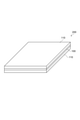
- the bonding substrate 200 is manufactured by using the ceramic plate 100. Therefore, the accuracy of alignment between the ceramic plate 100 and the metal plate 110 can be improved. Therefore, the positional deviation between the ceramic plate 100 and the metal plate 110 can be sufficiently reduced. Therefore, the bonded substrate 200 having excellent dimensional accuracy can be manufactured.
- the bonding substrate 200 includes a pair of metal plates 110 arranged so as to face each other, and a ceramic plate 100 between the pair of metal plates 110.
- the pair of metal plates 110 are joined to the ceramic plate 100 so as to cover the main surface 100A and the main surface 100B of the ceramic plate 100.
- Examples of the metal plate 110 include a copper plate.
- the shape and size of the ceramic plate 100 and the metal plate 110 may be the same or different.
- the bonded substrate 200 can be manufactured by the above-mentioned manufacturing method.
- a part of the metal plate 110 in the bonded substrate 200 is removed to form an independent conductor portion for each partition portion 11.
- Perform the process. This step may be performed, for example, by photolithography. Specifically, first, a resist having photosensitivity is printed on the main surface of the bonding substrate 200. Then, a resist pattern having a predetermined shape is formed by using an exposure apparatus. The resist may be a negative type or a positive type. The uncured resist is removed, for example, by washing.
- FIG. 10 is a perspective view showing an example of a bonding substrate 200 in which a resist pattern 30 is formed on a main surface 200A.
- FIG. 10 shows only the main surface 200A side, a similar resist pattern may be formed on the main surface 200B side.
- the resist pattern 30 is formed on the main surface 200A and the main surface 200B in the region corresponding to each section 11 of the ceramic plate 100. Also when forming the resist pattern 30, the positions of the corners 12 of the ceramic plate 100 and the corners 112 of the metal plate 110 may be detected by image processing to position the bonding substrate 200. As a result, the resist pattern 30 can be formed on the main surface 200A (main surface 200B) with high position accuracy.
- the portion of the metal plate 110 that is not covered by the resist pattern 30 is removed by etching. As a result, the main surface 100A and the main surface 100B of the ceramic plate 100 are exposed to the portion. After that, the resist pattern 30 is removed to form an independent conductor portion for each compartment 11.
- the circuit board 300 as shown in FIG. 11 is obtained.
- the resist pattern 30 may be formed on only one of the main surface 200A and the main surface 200B, and the conductor portion may be formed on only one of the main surfaces. In this case, a circuit board having a conductor portion on one main surface side of the ceramic plate 100 and a metal plate on the other main surface side can be obtained.
- the metal plate may function as a heat dissipation member.
- the circuit board 300 is manufactured by using the bonding board 200 provided with the ceramic plate 100. Since the bonding substrate 200 is excellent in dimensional accuracy, the bonding substrate 200 can be positioned with high accuracy when forming the resist pattern 30. Therefore, it is possible to manufacture a bonded substrate 200 having excellent positional accuracy between the ceramic plate 100 and the conductor portion 50. That is, the positional deviation between the ceramic plate 100 and the conductor portion 50 can be sufficiently reduced. Therefore, it is possible to manufacture the circuit board 300 having excellent dimensional accuracy.
- the circuit board 300 of FIG. 11 includes a ceramic plate 100 and a conductor portion 50 arranged to face each other with the ceramic plate 100 interposed therebetween.
- the conductor portion 50 is independently provided on the main surface 100A and the main surface 100B for each section 11. That is, each section 11 is provided with a pair of conductor portions 50 arranged so as to face each other.
- the circuit board 300 is cut along the scribe lines L1 and L2, and is divided into a plurality of divided boards and an outer edge portion 15. Since the scribe lines L1 and L2 are formed with high position accuracy, the divided substrate is excellent in dimensional accuracy.
- a split board is used as a component of, for example, a power module.
- electronic components are mounted on the conductor portion 50 of the divided substrate. Since the divided substrate is excellent in dimensional accuracy, the reliability of the power module can be improved. Further, since the size of the outer edge portion 15 is sufficiently small, the ceramic base material can be effectively used.
- the corner portion 12 of the ceramic plate 100 (101) may be chamfered.
- the corner portion 12 may have, for example, a C chamfered shape or an R chamfered shape.
- the ceramic plate may be in the shape of a disk having no corners. In this case, the entire circumferential side surface may be composed of a cut surface cut by a laser beam. Burrs and chips are suppressed on such sides, and warpage is also suppressed by microcracks on the sides. Therefore, the positioning of the ceramic plate can be performed with high accuracy based on an arbitrary location on the outer edge of the ceramic plate.
- the metal plate 110 is bonded to both main surfaces of the ceramic plate 100, but the bonding substrate 200 is not limited to this.
- the metal plate 110 may be joined to only one main surface of the ceramic plate 100.
- the shape of the conductor portion 50 provided in each compartment 11 of the circuit board 300 does not have to be the same, and in the modified example, the conductor portion may have a different shape for each compartment 11. Any surface treatment may be applied to the conductor portion 50 of the circuit board 300.
- a part of the surface of the conductor portion 50 may be covered with a protective layer such as a solder resist, and the other portion of the surface of the conductor portion 50 may be plated.
- a ceramic plate capable of positioning with high accuracy and a method for manufacturing the same. Further, by having such a ceramic plate, it is possible to provide a bonded substrate having excellent dimensional accuracy and a method for manufacturing the same, and a circuit board and a method for manufacturing the same.
Landscapes
- Engineering & Computer Science (AREA)
- Chemical & Material Sciences (AREA)
- Ceramic Engineering (AREA)
- Structural Engineering (AREA)
- Microelectronics & Electronic Packaging (AREA)
- Mechanical Engineering (AREA)
- Materials Engineering (AREA)
- Organic Chemistry (AREA)
- Manufacturing & Machinery (AREA)
- Physics & Mathematics (AREA)
- Plasma & Fusion (AREA)
- Optics & Photonics (AREA)
- Structure Of Printed Boards (AREA)
Priority Applications (1)
| Application Number | Priority Date | Filing Date | Title |
|---|---|---|---|
| JP2022544630A JPWO2022045140A1 (https=) | 2020-08-25 | 2021-08-24 |
Applications Claiming Priority (2)
| Application Number | Priority Date | Filing Date | Title |
|---|---|---|---|
| JP2020-141699 | 2020-08-25 | ||
| JP2020141699 | 2020-08-25 |
Publications (1)
| Publication Number | Publication Date |
|---|---|
| WO2022045140A1 true WO2022045140A1 (ja) | 2022-03-03 |
Family
ID=80353954
Family Applications (1)
| Application Number | Title | Priority Date | Filing Date |
|---|---|---|---|
| PCT/JP2021/031003 Ceased WO2022045140A1 (ja) | 2020-08-25 | 2021-08-24 | セラミック板及びその製造方法、接合基板及びその製造方法、並びに、回路基板及びその製造方法 |
Country Status (2)
| Country | Link |
|---|---|
| JP (1) | JPWO2022045140A1 (https=) |
| WO (1) | WO2022045140A1 (https=) |
Citations (4)
| Publication number | Priority date | Publication date | Assignee | Title |
|---|---|---|---|---|
| JPH08174244A (ja) * | 1994-12-20 | 1996-07-09 | Hitachi Cable Ltd | 基板材料の切断方法及びその装置 |
| JP2001053443A (ja) * | 1999-08-06 | 2001-02-23 | Hitachi Ltd | 電子回路基板の製造方法,電子回路基板の製造装置及び電子回路基板 |
| JP2008198905A (ja) * | 2007-02-15 | 2008-08-28 | Hitachi Metals Ltd | セラミックス基板及びセラミックス回路基板の製造方法並びに集合基板と半導体モジュール |
| JP2017065935A (ja) * | 2015-09-28 | 2017-04-06 | デンカ株式会社 | セラミックス回路基板 |
Family Cites Families (3)
| Publication number | Priority date | Publication date | Assignee | Title |
|---|---|---|---|---|
| JP5574848B2 (ja) * | 2010-02-24 | 2014-08-20 | 京セラ株式会社 | 多数個取り配線基板 |
| JP6034158B2 (ja) * | 2012-11-29 | 2016-11-30 | 京セラ株式会社 | 配線基板およびそれを用いた実装構造体 |
| JP7270525B2 (ja) * | 2019-10-31 | 2023-05-10 | デンカ株式会社 | 複合基板及びその製造方法、並びに、回路基板の製造方法 |
-
2021
- 2021-08-24 JP JP2022544630A patent/JPWO2022045140A1/ja active Pending
- 2021-08-24 WO PCT/JP2021/031003 patent/WO2022045140A1/ja not_active Ceased
Patent Citations (4)
| Publication number | Priority date | Publication date | Assignee | Title |
|---|---|---|---|---|
| JPH08174244A (ja) * | 1994-12-20 | 1996-07-09 | Hitachi Cable Ltd | 基板材料の切断方法及びその装置 |
| JP2001053443A (ja) * | 1999-08-06 | 2001-02-23 | Hitachi Ltd | 電子回路基板の製造方法,電子回路基板の製造装置及び電子回路基板 |
| JP2008198905A (ja) * | 2007-02-15 | 2008-08-28 | Hitachi Metals Ltd | セラミックス基板及びセラミックス回路基板の製造方法並びに集合基板と半導体モジュール |
| JP2017065935A (ja) * | 2015-09-28 | 2017-04-06 | デンカ株式会社 | セラミックス回路基板 |
Also Published As
| Publication number | Publication date |
|---|---|
| JPWO2022045140A1 (https=) | 2022-03-03 |
Similar Documents
| Publication | Publication Date | Title |
|---|---|---|
| JP7465879B2 (ja) | セラミックス基板及びその製造方法、複合基板及びその製造方法、並びに、回路基板及びその製造方法 | |
| CN105705468B (zh) | 激光加工方法以及激光加工装置 | |
| JP7270525B2 (ja) | 複合基板及びその製造方法、並びに、回路基板の製造方法 | |
| JP2022132865A (ja) | 絶縁回路基板の製造方法 | |
| WO2022045140A1 (ja) | セラミック板及びその製造方法、接合基板及びその製造方法、並びに、回路基板及びその製造方法 | |
| JPH04343287A (ja) | 回路基板 | |
| CN114380614A (zh) | 高刻蚀精度陶瓷覆金属板、制备方法及芯片封装模块 | |
| JP7573023B2 (ja) | 窒化ケイ素板及びその製造方法、複合基板及びその製造方法、並びに、回路基板及びその製造方法 | |
| JP7165842B1 (ja) | セラミック板、及びセラミック板の製造方法 | |
| JP2008041945A (ja) | パワーモジュール用基板の製造方法およびパワーモジュール用基板並びにパワーモジュール | |
| JP7621339B2 (ja) | 窒化アルミニウム板及びその製造方法、複合基板及びその製造方法、並びに、回路基板及びその製造方法 | |
| WO2022131337A1 (ja) | セラミック板及びその製造方法、複合基板及びその製造方法、並びに、回路基板及びその製造方法 | |
| JP4881557B2 (ja) | チップ抵抗器の製造方法 | |
| JP4663899B2 (ja) | 回路基板の製造方法 | |
| JP7490934B2 (ja) | 回路基板の製造方法及び回路基板 | |
| WO2023008199A1 (ja) | 接合基板、回路基板及びその製造方法、並びに、個片基板及びその製造方法 | |
| JP2025115648A (ja) | セラミック基板及びその製造方法、セラミック板、集合回路基板、並びに回路基板 | |
| JP3712378B2 (ja) | 端子付き回路基板及びその製造方法 | |
| JP7484109B2 (ja) | 窒化珪素セラミックス焼結基板の製造方法及び回路基板の製造方法 | |
| JP7580188B2 (ja) | 窒化珪素セラミックス焼結基板の製造方法及び回路基板の製造方法 | |
| EP4369874A1 (en) | Bonded substrate, circuit board and manufacturing method therefor, and individual substrate and manufacturing method therefor | |
| JP2012142490A (ja) | マーキング方法 | |
| JP7581196B2 (ja) | 複合基板、複合基板の製造方法、回路基板の製造方法、複数の回路基板の集合体の製造方法及び複数の回路基板の製造方法 | |
| JP2013182989A (ja) | 金属−セラミックス接合回路基板の製造方法 | |
| JP2019067854A (ja) | 金属−セラミックス接合回路基板の製造方法 |
Legal Events
| Date | Code | Title | Description |
|---|---|---|---|
| 121 | Ep: the epo has been informed by wipo that ep was designated in this application |
Ref document number: 21861565 Country of ref document: EP Kind code of ref document: A1 |
|
| ENP | Entry into the national phase |
Ref document number: 2022544630 Country of ref document: JP Kind code of ref document: A |
|
| NENP | Non-entry into the national phase |
Ref country code: DE |
|
| 122 | Ep: pct application non-entry in european phase |
Ref document number: 21861565 Country of ref document: EP Kind code of ref document: A1 |