WO2022044641A1 - シリコン単結晶基板の製造方法及びシリコン単結晶基板 - Google Patents
シリコン単結晶基板の製造方法及びシリコン単結晶基板 Download PDFInfo
- Publication number
- WO2022044641A1 WO2022044641A1 PCT/JP2021/027435 JP2021027435W WO2022044641A1 WO 2022044641 A1 WO2022044641 A1 WO 2022044641A1 JP 2021027435 W JP2021027435 W JP 2021027435W WO 2022044641 A1 WO2022044641 A1 WO 2022044641A1
- Authority
- WO
- WIPO (PCT)
- Prior art keywords
- single crystal
- silicon single
- crystal substrate
- carbon
- film
- Prior art date
- Legal status (The legal status is an assumption and is not a legal conclusion. Google has not performed a legal analysis and makes no representation as to the accuracy of the status listed.)
- Ceased
Links
Images





Classifications
-
- C—CHEMISTRY; METALLURGY
- C30—CRYSTAL GROWTH
- C30B—SINGLE-CRYSTAL GROWTH; UNIDIRECTIONAL SOLIDIFICATION OF EUTECTIC MATERIAL OR UNIDIRECTIONAL DEMIXING OF EUTECTOID MATERIAL; REFINING BY ZONE-MELTING OF MATERIAL; PRODUCTION OF A HOMOGENEOUS POLYCRYSTALLINE MATERIAL WITH DEFINED STRUCTURE; SINGLE CRYSTALS OR HOMOGENEOUS POLYCRYSTALLINE MATERIAL WITH DEFINED STRUCTURE; AFTER-TREATMENT OF SINGLE CRYSTALS OR A HOMOGENEOUS POLYCRYSTALLINE MATERIAL WITH DEFINED STRUCTURE; APPARATUS THEREFOR
- C30B33/00—After-treatment of single crystals or homogeneous polycrystalline material with defined structure
- C30B33/02—Heat treatment
-
- H—ELECTRICITY
- H10—SEMICONDUCTOR DEVICES; ELECTRIC SOLID-STATE DEVICES NOT OTHERWISE PROVIDED FOR
- H10P—GENERIC PROCESSES OR APPARATUS FOR THE MANUFACTURE OR TREATMENT OF DEVICES COVERED BY CLASS H10
- H10P14/00—Formation of materials, e.g. in the shape of layers or pillars
- H10P14/20—Formation of materials, e.g. in the shape of layers or pillars of semiconductor materials
- H10P14/34—Deposited materials, e.g. layers
- H10P14/3402—Deposited materials, e.g. layers characterised by the chemical composition
- H10P14/3404—Deposited materials, e.g. layers characterised by the chemical composition being Group IVA materials
- H10P14/3408—Silicon carbide
-
- C—CHEMISTRY; METALLURGY
- C30—CRYSTAL GROWTH
- C30B—SINGLE-CRYSTAL GROWTH; UNIDIRECTIONAL SOLIDIFICATION OF EUTECTIC MATERIAL OR UNIDIRECTIONAL DEMIXING OF EUTECTOID MATERIAL; REFINING BY ZONE-MELTING OF MATERIAL; PRODUCTION OF A HOMOGENEOUS POLYCRYSTALLINE MATERIAL WITH DEFINED STRUCTURE; SINGLE CRYSTALS OR HOMOGENEOUS POLYCRYSTALLINE MATERIAL WITH DEFINED STRUCTURE; AFTER-TREATMENT OF SINGLE CRYSTALS OR A HOMOGENEOUS POLYCRYSTALLINE MATERIAL WITH DEFINED STRUCTURE; APPARATUS THEREFOR
- C30B29/00—Single crystals or homogeneous polycrystalline material with defined structure characterised by the material or by their shape
- C30B29/02—Elements
- C30B29/06—Silicon
-
- C—CHEMISTRY; METALLURGY
- C30—CRYSTAL GROWTH
- C30B—SINGLE-CRYSTAL GROWTH; UNIDIRECTIONAL SOLIDIFICATION OF EUTECTIC MATERIAL OR UNIDIRECTIONAL DEMIXING OF EUTECTOID MATERIAL; REFINING BY ZONE-MELTING OF MATERIAL; PRODUCTION OF A HOMOGENEOUS POLYCRYSTALLINE MATERIAL WITH DEFINED STRUCTURE; SINGLE CRYSTALS OR HOMOGENEOUS POLYCRYSTALLINE MATERIAL WITH DEFINED STRUCTURE; AFTER-TREATMENT OF SINGLE CRYSTALS OR A HOMOGENEOUS POLYCRYSTALLINE MATERIAL WITH DEFINED STRUCTURE; APPARATUS THEREFOR
- C30B31/00—Diffusion or doping processes for single crystals or homogeneous polycrystalline material with defined structure; Apparatus therefor
- C30B31/06—Diffusion or doping processes for single crystals or homogeneous polycrystalline material with defined structure; Apparatus therefor by contacting with diffusion material in the gaseous state
-
- C—CHEMISTRY; METALLURGY
- C30—CRYSTAL GROWTH
- C30B—SINGLE-CRYSTAL GROWTH; UNIDIRECTIONAL SOLIDIFICATION OF EUTECTIC MATERIAL OR UNIDIRECTIONAL DEMIXING OF EUTECTOID MATERIAL; REFINING BY ZONE-MELTING OF MATERIAL; PRODUCTION OF A HOMOGENEOUS POLYCRYSTALLINE MATERIAL WITH DEFINED STRUCTURE; SINGLE CRYSTALS OR HOMOGENEOUS POLYCRYSTALLINE MATERIAL WITH DEFINED STRUCTURE; AFTER-TREATMENT OF SINGLE CRYSTALS OR A HOMOGENEOUS POLYCRYSTALLINE MATERIAL WITH DEFINED STRUCTURE; APPARATUS THEREFOR
- C30B33/00—After-treatment of single crystals or homogeneous polycrystalline material with defined structure
- C30B33/005—Oxydation
-
- C—CHEMISTRY; METALLURGY
- C30—CRYSTAL GROWTH
- C30B—SINGLE-CRYSTAL GROWTH; UNIDIRECTIONAL SOLIDIFICATION OF EUTECTIC MATERIAL OR UNIDIRECTIONAL DEMIXING OF EUTECTOID MATERIAL; REFINING BY ZONE-MELTING OF MATERIAL; PRODUCTION OF A HOMOGENEOUS POLYCRYSTALLINE MATERIAL WITH DEFINED STRUCTURE; SINGLE CRYSTALS OR HOMOGENEOUS POLYCRYSTALLINE MATERIAL WITH DEFINED STRUCTURE; AFTER-TREATMENT OF SINGLE CRYSTALS OR A HOMOGENEOUS POLYCRYSTALLINE MATERIAL WITH DEFINED STRUCTURE; APPARATUS THEREFOR
- C30B33/00—After-treatment of single crystals or homogeneous polycrystalline material with defined structure
- C30B33/08—Etching
- C30B33/10—Etching in solutions or melts
-
- C—CHEMISTRY; METALLURGY
- C30—CRYSTAL GROWTH
- C30B—SINGLE-CRYSTAL GROWTH; UNIDIRECTIONAL SOLIDIFICATION OF EUTECTIC MATERIAL OR UNIDIRECTIONAL DEMIXING OF EUTECTOID MATERIAL; REFINING BY ZONE-MELTING OF MATERIAL; PRODUCTION OF A HOMOGENEOUS POLYCRYSTALLINE MATERIAL WITH DEFINED STRUCTURE; SINGLE CRYSTALS OR HOMOGENEOUS POLYCRYSTALLINE MATERIAL WITH DEFINED STRUCTURE; AFTER-TREATMENT OF SINGLE CRYSTALS OR A HOMOGENEOUS POLYCRYSTALLINE MATERIAL WITH DEFINED STRUCTURE; APPARATUS THEREFOR
- C30B33/00—After-treatment of single crystals or homogeneous polycrystalline material with defined structure
- C30B33/08—Etching
- C30B33/12—Etching in gas atmosphere or plasma
-
- H—ELECTRICITY
- H10—SEMICONDUCTOR DEVICES; ELECTRIC SOLID-STATE DEVICES NOT OTHERWISE PROVIDED FOR
- H10P—GENERIC PROCESSES OR APPARATUS FOR THE MANUFACTURE OR TREATMENT OF DEVICES COVERED BY CLASS H10
- H10P14/00—Formation of materials, e.g. in the shape of layers or pillars
- H10P14/20—Formation of materials, e.g. in the shape of layers or pillars of semiconductor materials
-
- H—ELECTRICITY
- H10—SEMICONDUCTOR DEVICES; ELECTRIC SOLID-STATE DEVICES NOT OTHERWISE PROVIDED FOR
- H10P—GENERIC PROCESSES OR APPARATUS FOR THE MANUFACTURE OR TREATMENT OF DEVICES COVERED BY CLASS H10
- H10P14/00—Formation of materials, e.g. in the shape of layers or pillars
- H10P14/20—Formation of materials, e.g. in the shape of layers or pillars of semiconductor materials
- H10P14/29—Formation of materials, e.g. in the shape of layers or pillars of semiconductor materials characterised by the substrates
- H10P14/2901—Materials
- H10P14/2902—Materials being Group IVA materials
- H10P14/2905—Silicon, silicon germanium or germanium
-
- H—ELECTRICITY
- H10—SEMICONDUCTOR DEVICES; ELECTRIC SOLID-STATE DEVICES NOT OTHERWISE PROVIDED FOR
- H10P—GENERIC PROCESSES OR APPARATUS FOR THE MANUFACTURE OR TREATMENT OF DEVICES COVERED BY CLASS H10
- H10P36/00—Gettering within semiconductor bodies
-
- H—ELECTRICITY
- H10—SEMICONDUCTOR DEVICES; ELECTRIC SOLID-STATE DEVICES NOT OTHERWISE PROVIDED FOR
- H10P—GENERIC PROCESSES OR APPARATUS FOR THE MANUFACTURE OR TREATMENT OF DEVICES COVERED BY CLASS H10
- H10P30/00—Ion implantation into wafers, substrates or parts of devices
- H10P30/20—Ion implantation into wafers, substrates or parts of devices into semiconductor materials, e.g. for doping
- H10P30/202—Ion implantation into wafers, substrates or parts of devices into semiconductor materials, e.g. for doping characterised by the semiconductor materials
- H10P30/204—Ion implantation into wafers, substrates or parts of devices into semiconductor materials, e.g. for doping characterised by the semiconductor materials into Group IV semiconductors
-
- H—ELECTRICITY
- H10—SEMICONDUCTOR DEVICES; ELECTRIC SOLID-STATE DEVICES NOT OTHERWISE PROVIDED FOR
- H10P—GENERIC PROCESSES OR APPARATUS FOR THE MANUFACTURE OR TREATMENT OF DEVICES COVERED BY CLASS H10
- H10P30/00—Ion implantation into wafers, substrates or parts of devices
- H10P30/20—Ion implantation into wafers, substrates or parts of devices into semiconductor materials, e.g. for doping
- H10P30/208—Ion implantation into wafers, substrates or parts of devices into semiconductor materials, e.g. for doping of electrically inactive species
-
- H—ELECTRICITY
- H10—SEMICONDUCTOR DEVICES; ELECTRIC SOLID-STATE DEVICES NOT OTHERWISE PROVIDED FOR
- H10P—GENERIC PROCESSES OR APPARATUS FOR THE MANUFACTURE OR TREATMENT OF DEVICES COVERED BY CLASS H10
- H10P36/00—Gettering within semiconductor bodies
- H10P36/20—Intrinsic gettering, i.e. thermally inducing defects by using oxygen present in the silicon body
-
- Y—GENERAL TAGGING OF NEW TECHNOLOGICAL DEVELOPMENTS; GENERAL TAGGING OF CROSS-SECTIONAL TECHNOLOGIES SPANNING OVER SEVERAL SECTIONS OF THE IPC; TECHNICAL SUBJECTS COVERED BY FORMER USPC CROSS-REFERENCE ART COLLECTIONS [XRACs] AND DIGESTS
- Y02—TECHNOLOGIES OR APPLICATIONS FOR MITIGATION OR ADAPTATION AGAINST CLIMATE CHANGE
- Y02P—CLIMATE CHANGE MITIGATION TECHNOLOGIES IN THE PRODUCTION OR PROCESSING OF GOODS
- Y02P70/00—Climate change mitigation technologies in the production process for final industrial or consumer products
- Y02P70/50—Manufacturing or production processes characterised by the final manufactured product
Definitions
- the present invention relates to a silicon single crystal substrate having a carbon diffusion layer on its surface and a method for manufacturing the same.
- Patent Document 1 discloses that slip dislocations are suppressed by performing RTA treatment in a nitrogen-containing gas atmosphere.
- Patent Document 2 discloses that heat treatment is performed in an atmosphere containing a carbon-containing gas so that the carbon concentration reaches saturation at any position where the distance from the surface in the depth direction is 5 ⁇ m or less.
- the saturation concentration of the carbon concentration in this case is the solid solubility of carbon at the maximum temperature at the time of heat treatment.
- the saturation concentration of carbon when the silicon wafer is heated at 1200 ° C. is 11 ⁇ 10 16 atoms / cm 3 . It is stated that.
- Patent Document 3 discloses a method for manufacturing an epitaxial silicon wafer in which a carbon diffusion layer is formed on a surface layer by performing heat treatment in a carbon-containing gas atmosphere, and an epitaxial layer is formed on the carbon diffusion layer.
- Japanese Unexamined Patent Publication No. 2002-110685 Japanese Unexamined Patent Publication No. 2018-190903 Japanese Unexamined Patent Publication No. 2020-43232 Japanese Unexamined Patent Publication No. 2016-111044
- Patent Document 2 is insufficient, and it is necessary to form a carbon diffusion layer having a concentration higher than the saturation concentration in order to suppress slip dislocations more reliably.
- the peak concentration of the carbon diffusion layer described in Patent Document 3 is as high as 1 ⁇ 10 18 to 1 ⁇ 10 20 atoms / cm 3 , but the thickness of the carbon diffusion layer is 200 nm or less, and the thickness is high. It was thin and insufficient to more reliably suppress slip dislocations.
- the present invention has been made to solve the above problems, and is a silicon single crystal substrate having proximity gettering ability, high strength near the surface, and resistance to dislocation generation and dislocation extension, and a method for manufacturing the same.
- the purpose is to provide.
- the present invention has been made to achieve the above object, and is a method for manufacturing a silicon single crystal substrate having a carbon diffusion layer on the surface, by RTA-treating the silicon single crystal substrate in a carbon-containing gas atmosphere.
- the 3C-SiC single crystal film is oxidized to form an oxide film and into the silicon single crystal substrate.
- a method for manufacturing a silicon single crystal substrate which comprises a step of inwardly diffusing carbon and a step of removing the oxide film.
- the method for manufacturing the silicon single crystal substrate in which the temperature of the RTA treatment is less than 800 ° C. can be used.
- RTA treatment at 1150 ° C. to 1300 ° C. was performed in a carbon-containing gas atmosphere, and the surface of the silicon single crystal substrate was 7 nm or less. It can be used as a method for manufacturing a silicon single crystal substrate for forming a 3C-SiC single crystal film having a thickness of.
- RTA at 1150 ° C. to 1400 ° C. for 1 to 60 seconds in an oxygen atmosphere. It can be a method for manufacturing a silicon single crystal substrate to be treated.
- a carbon diffusion layer having a carbon concentration of 1 ⁇ 10 17 atoms / cm 3 or more and a thickness of 2 ⁇ m or more can be stably formed on the surface of the silicon single crystal substrate.
- the step of removing the oxide film it is possible to use a method for manufacturing a silicon single crystal substrate in which the oxide film is etched by RTA treatment at 1150 ° C. to 1400 ° C. for 1 to 60 seconds in a hydrogen atmosphere.
- the RTA processing up to the previous process can be performed with the same device, so that the processing can be performed easily and with high productivity.
- a silicon single crystal substrate that is etched with 0.1 to 5.0% hydrofluoric acid (HF aqueous solution) for less than 10 minutes and then rinsed with pure water.
- HF aqueous solution hydrofluoric acid
- the silicon single crystal substrate is obtained by repeating the steps of oxidizing the 3C-SiC single crystal film to form an oxide film and inwardly diffusing carbon into the silicon single crystal substrate and removing the oxide film. It can be a manufacturing method.
- the method for manufacturing a silicon epitaxial wafer in which an epitaxial layer is formed on the silicon single crystal substrate manufactured by the method for manufacturing a silicon single crystal substrate can be used.
- the present invention is a silicon single crystal substrate provided with a carbon diffusion layer on the surface, wherein the carbon diffusion layer has a carbon concentration of 1 ⁇ 10 17 atoms / cm 3 or more and a thickness of 2 ⁇ m or more.
- a crystalline substrate can be provided.
- silicon single crystal substrate According to such a silicon single crystal substrate, it is a silicon single crystal substrate having proximity gettering ability, high strength near the surface, and dislocation generation and dislocation are difficult to extend.
- a silicon epitaxial wafer having an epitaxial layer on the carbon diffusion layer in the silicon single crystal substrate can be obtained.
- silicon epitaxial wafer it is a silicon epitaxial wafer that has proximity gettering ability, has high strength near the surface, and is difficult to generate dislocations or dislocations.
- a silicon single crystal substrate having proximity gettering ability, high strength near the surface, and resistance to dislocation generation and dislocation extension As described above, according to the method for manufacturing a silicon single crystal substrate of the present invention, there is provided a silicon single crystal substrate having proximity gettering ability, high strength near the surface, and resistance to dislocation generation and dislocation extension. It becomes possible to do. According to the silicon single crystal substrate of the present invention, the silicon single crystal substrate has a proximity gettering ability and high strength near the surface, so that dislocations and dislocations are difficult to spread.
- the outline of the manufacturing process of the silicon single crystal substrate having a carbon diffusion layer is shown.
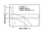
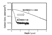
- a comparison of carbon concentrations in a silicon single crystal substrate is shown. It is a figure which showed the comparison of the carbon concentration distribution before and after the RTA treatment of an oxygen atmosphere. It is a figure which showed how the carbon concentration distribution becomes gentle by repeating RTA in an oxygen atmosphere.
- the evaluation results (SIMS, rosette test) of the silicon single crystal substrate according to Example 1 and Comparative Example 1 are shown.
- the SEM observation result of the silicon single crystal substrate which concerns on Example 2 is shown.
- the SIMS measurement result of the silicon single crystal substrate (heat treatment temperature: 1150 ° C.) which concerns on Example 2 is shown.
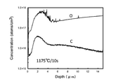
- the SIMS measurement result of the silicon single crystal substrate (heat treatment temperature: 1175 ° C.) which concerns on Example 2 is shown.
- the SIMS measurement result of the silicon single crystal substrate (heat treatment temperature: 1200 ° C.) which concerns on Example 2 is shown.
- the SIMS measurement result of the silicon epitaxial wafer which concerns on Example 3 is shown.
- the SEM observation result of the silicon epitaxial wafer according to Example 3 is shown.
- the present inventors can solve the above-mentioned problems by forming a thick carbon diffusion layer having a carbon concentration higher than the solid solubility and a thickness of 2 ⁇ m or more as the surface layer of the silicon single crystal substrate. I found that. Then, a 3C-SiC single crystal film is formed on the surface of the silicon single crystal substrate, and then an oxidation treatment is performed to change the 3C-SiC single crystal film into an oxide film and at the same time diffuse carbon on the surface layer of the silicon substrate. We have found that it is possible to form a thick carbon diffusion layer having a high carbon concentration of 2 ⁇ m or more, and completed the present invention.
- the present inventors have developed a method for manufacturing a silicon single crystal substrate having a carbon diffusion layer on the surface by performing RTA treatment on the silicon single crystal substrate in a carbon-containing gas atmosphere.
- RTA-treating the silicon single crystal substrate on which the 3C-SiC single crystal film is formed in an oxidizing atmosphere the 3C-SiC single crystal film is oxidized to form an oxide film and carbon is contained in the silicon single crystal substrate.
- the method of manufacturing a silicon single crystal substrate including a step of inwardly diffusing We have found that it is possible to manufacture a difficult-to-difficult silicon single crystal substrate, and completed the present invention.
- the present inventors are silicon single crystal substrates having a carbon diffusion layer on the surface, and the carbon diffusion layer has a carbon concentration of 1 ⁇ 10 17 atoms / cm 3 or more and a thickness of 2 ⁇ m or more.
- the present invention has been completed by finding that a silicon single crystal substrate has a proximity gettering ability, high strength near the surface, and a silicon single crystal substrate in which dislocations and dislocations are less likely to occur and spread.
- FIG. 1 is a diagram showing an outline of a manufacturing process of a silicon single crystal substrate having a carbon diffusion layer according to the present invention, which will be described later, and FIG. 1 (E) shows the silicon single crystal substrate according to the present invention.
- the silicon single crystal substrate according to the present invention is provided with a carbon diffusion layer 5 on the surface of the silicon single crystal substrate 1, and the carbon diffusion layer 5 has a carbon concentration of 1 ⁇ 10 17 Atoms / cm 3 or more and a thickness of 2 ⁇ m or more.
- the silicon single crystal substrate having such a carbon diffusion layer 5 has a proximity gettering ability and high strength near the surface, and it is difficult for dislocations to occur or dislocations to spread.
- the upper limit of the carbon concentration in the carbon diffusion layer 5 and the thickness of the carbon diffusion layer 5 can be appropriately adjusted depending on the RTA treatment conditions and the number of RTA treatments, and are not particularly limited, but the carbon concentration is, for example, 1 ⁇ . It can be 10 19 atoms / cm 3 or less. The thickness can be, for example, 5 ⁇ m or less.
- Any silicon single crystal substrate can be used regardless of the defect region, diameter, conductivity (mold, resistivity), etc. of the crystal.
- a silicon single crystal substrate obtained by slicing from a silicon single crystal ingot grown by the Czochralski method can be used.
- a silicon single crystal substrate having a defect-free region is preferable so as not to deteriorate the device characteristics.
- any silicon single crystal substrate may be used, and of course, a silicon single crystal substrate having a defect-free region can also be used.
- Silicon epitaxial wafer As shown in FIG. 1 (F), it is also preferable to use a silicon epitaxial wafer in which the epitaxial layer 6 is provided on the carbon diffusion layer 5 of the silicon single crystal substrate.
- a silicon epitaxial wafer has a defect-free epitaxial layer on the surface thereof, has a proximity gettering function immediately below the layer, and is less likely to cause dislocations.
- FIG. 1 shows an outline of a manufacturing process of a silicon single crystal substrate having a carbon diffusion layer according to the present invention.
- the silicon single crystal substrate 1 is prepared (FIG. 1 (A)).
- the silicon single crystal substrate 1 according to the present invention may be any silicon single crystal substrate.
- Step of adhering carbon to the surface of a silicon single crystal substrate RTA treatment is performed in a carbon-containing gas atmosphere (FIG. 1 (B)).
- the carbon-containing gas atmosphere at this time can be, for example, a mixed atmosphere of any one of CH 4 , C 2 H 4 , and C 3 H 8 gas and Ar + H 2 .
- the carbon concentration at this time is preferably 0.5% or more and less than 10%.
- the RTA conditions are not particularly limited as long as carbon 2 can be attached to the surface of the silicon single crystal substrate 1, but are low temperature conditions, for example, 600 ° C. or higher, less than 800 ° C., and 1 to 60 seconds. be able to.
- the heat treatment temperature of a general RTA device is 600 ° C or higher.
- the heat treatment temperature is 600 ° C. or higher, carbon can be reliably adhered to and bonded to the silicon on the surface of the substrate.
- the heat treatment temperature becomes 800 ° C. or higher, the silicon starts to evaporate from the surface of the substrate, and the bonded carbon and silicon are lost from the surface of the substrate, which may cause unstable carbon adhesion. Therefore, in order to stably adhere carbon, the temperature is preferably less than 800 ° C.
- Step of forming a 3C-SiC single crystal film on the surface of a silicon single crystal substrate Next, the carbon 2 and the silicon of the silicon single crystal substrate 1 are reacted to form a 3C—SiC single crystal film 3 on the surface of the silicon single crystal substrate 1 (FIG. 1 (C)). At this time, the silicon on the surface of the silicon single crystal substrate 1 reacts with the carbon 2 adhering to the surface of the silicon single crystal substrate 1 to form a single crystal, which becomes a seed crystal and is thin 3C on the surface of the silicon single crystal substrate 1. -SiC single crystal film 3 is formed.
- the treatment conditions at this time are not particularly limited, and may be any conditions as long as carbon and silicon react to form a 3C-SiC single crystal film.
- a carbon-containing gas atmosphere it is possible to perform RTA treatment at a higher temperature than when carbon is attached.
- the RTA treatment is efficient because it can be treated in the same device following the previous step of adhering carbon, and there is no concern about contamination due to movement between devices as in the case of using another device.
- the carbon-containing gas atmosphere at this time is preferably set to the same conditions as in the step of adhering carbon to the surface of the silicon single crystal substrate. Specific RTA conditions can be 1150 ° C to 1300 ° C and 1 to 60 seconds.
- a 3C-SiC single crystal film 3 having a diameter of 7 nm or less is stably formed on the surface of a silicon single crystal substrate.
- the carbonization of silicon on the surface of the silicon single crystal substrate 1 does not proceed any more, and the thickness of the 3C-SiC single crystal film 3 is limited to 7 nm. Will be.
- the RTA conditions in this step can be, for example, an oxygen atmosphere, 1150 ° C to 1400 ° C, and 1 to 60 seconds. Under such conditions, a carbon diffusion layer 5 having a carbon concentration of 1 ⁇ 10 17 atoms / cm 3 or more and a thickness of 2 ⁇ m or more can be stably formed on the surface of the silicon single crystal substrate 1.
- Carbon is present in the 3C-SiC single crystal film 3 at a density on the order of 10 22 atoms / cm 3 . Then, the carbon in the 3C—SiC single crystal film 3 is inwardly diffused into the silicon single crystal substrate 1 by the RTA treatment in the oxidizing atmosphere. This continues until all the 3C-SiC single crystal film 3 is changed to the oxide film 4, so that it is much higher than, for example, 3 ⁇ 10 16 atoms / cm 3 which is the solid solubility of carbon at 1200 ° C. 1 ⁇ 10 18 atoms / cm.
- a carbon diffusion layer 5 having a peak concentration of 3 or more can be formed on the surface.
- FIG. 2 shows a comparison of carbon concentrations in a silicon single crystal substrate.
- the carbon concentration at the 3C-SiC / Si interface becomes about 10 22 atoms / cm 3 , and carbon diffuses inward toward the silicon substrate due to the concentration gradient in the RTA treatment step. do.
- the region higher than the solid solubility carbon clusters and precipitates as in the region A in FIG.
- a carbon diffusion layer having a carbon concentration exceeding the solid solubility of carbon is formed as shown in the region B of FIG. Since carbon is supplied by inward diffusion, the carbon concentration decreases as the distance from the substrate surface increases.
- the region C in FIG. 2 shows a case where the carbon diffusion layer is formed by heat treatment in a carbon-containing gas atmosphere as described in Patent Document 2, and the carbon concentration in the carbon diffusion layer is solid-dissolved. It shows that it cannot be higher than the degree.
- the carbon concentration of the carbon diffusion layer 5 becomes equal to or higher than the solid solubility, and the high-concentration carbon diffusion layer 5 is thickened. Can be formed.
- a silicon single crystal substrate provided with a carbon diffusion layer is used as a substrate for a silicon epitaxial wafer, it is preferable that the peak value of the carbon concentration is close to the surface of the substrate.
- a silicon single crystal substrate provided with a carbon diffusion layer is used as a silicon single crystal substrate for device formation, a defect-free DZ layer is formed on the surface so that a peak value of carbon concentration exists immediately below the DZ layer. It is preferable to do so. Since the position where the peak value of the carbon concentration is formed is determined by the RTA condition, the optimum RTA condition can be determined according to the application of the silicon single crystal substrate.
- FIG. 3 is a diagram comparing the carbon concentrations in the vicinity of the surface before and after the RTA treatment in the oxygen atmosphere, and is a diagram showing how the high concentration carbon was diffused by the RTA treatment in the oxidizing atmosphere.
- FIG. 4 is a diagram showing how carbon is further diffused inside and the carbon concentration distribution becomes gentle by repeating RTA in an oxygen atmosphere.
- the oxide film 4 is removed (FIG. 1 (E)).
- the treatment method for removing the oxide film 4 is not particularly limited, but the oxide film 4 can be removed by the following method.
- a first method for removing the oxide film there is a method of etching and removing the oxide film by RTA treatment in a hydrogen (H 2 ) atmosphere.
- the treatment can be performed at 1150 ° C. to 1400 ° C. for 1 to 60 seconds in an H2 atmosphere.
- the treatment of removing the oxide film can be continued by using the RTA apparatus which has performed the steps of oxidizing the 3C-SiC single crystal film and diffusing the carbon. It's simple. However, in this method, even if the silicon single crystal substrate after being taken out from the RTA processing apparatus is visually observed, it is not clear whether or not the oxide film can be completely removed. Therefore, after that, hydrofluoric acid (HF aqueous solution) is used. It is more preferable to perform etching with.
- HF aqueous solution hydrofluoric acid
- the carbon in the carbon diffusion layer formed on the surface is re-diffused. It is preferable to determine the RTA conditions for the subsequent hydrogen atmosphere. If the 3C-SiC single crystal film is not completely converted into an oxide film and still exists, carbon diffusion from the 3C-SiC single crystal film continues even in the step of etching and removing the oxide film. Will be done.
- the oxide film can be removed by a wet treatment using hydrofluoric acid (HF aqueous solution).
- hydrofluoric acid HF aqueous solution
- HF aqueous solution hydrofluoric acid
- the carbon of the carbon diffusion layer is not re-diffused, and it can be easily confirmed that the surface of the silicon single crystal substrate is a hydrophobic surface, so that the residual 3C-SiC single crystal film remains. It is suitable as a method for confirming that the oxide film is completely removed.
- the first oxide film removing method (RTA treatment of hydrogen atmosphere) and the second oxide film removing method (wet treatment of hydrofluoric acid) can also be combined.
- RTA treatment of hydrogen atmosphere the silicon single crystal substrate was taken out from the RTA treatment device, and then etching with hydrofluoric acid (HF aqueous solution) was performed, it was visually confirmed that the oxide film was completely removed. It is also effective to check with.
- the oxide film is used. It is preferable to perform a step of removing the oxide film by changing the amount of the change to the above, changing the remaining 3C-SiC single crystal film into an oxide film again, and then removing the oxide film.
- the peak value and peak position of the carbon concentration of the carbon diffusion layer also change by repeating the steps of oxidation of the 3C-SiC single crystal film and carbon diffusion, so the RTA conditions should be determined in consideration of these effects. Is preferable.
- DSP polish
- An epitaxial layer 6 having a desired conductivity type, resistivity, and thickness can be formed on the silicon single crystal substrate 1 having the carbon diffusion layer 5 on the surface obtained as described above (FIG. 1 (FIG. 1). F)).
- Example 1 A silicon single crystal substrate as shown below was prepared. Diameter: 200 mm, (100), P type, resistivity 14 to 25 ⁇ ⁇ cm Oxygen concentration: 11,13 ppma (JEITA) Crystal region: NPC region (defect-free region)
- the RTA treatment conditions were CH 4 / Ar + H 2 (carbon concentration 1.4%) atmosphere, room temperature to 800 ° C., and holding at 800 ° C. for 20 sec.
- an RTA treatment was performed in which carbon adhering to the surface of the silicon single crystal substrate was reacted with silicon of the silicon single crystal substrate to change it into a 3C-SiC single crystal film.
- the RTA treatment conditions were CH 4 / Ar + H 2 (carbon concentration 1.4%) atmosphere and 10 sec at 1200 ° C. As a result, a 2 nm 3C-SiC single crystal film was formed on the surface.
- RTA treatment was performed to oxidize the 3C-SiC single crystal film and diffuse carbon.
- the RTA treatment conditions were O 2 atmosphere, 1250 ° C., and 30 sec.
- RTA treatment and wet etching for removing the oxide film were performed.
- the RTA treatment conditions were H 2 atmosphere, 1250 ° C., and 30 sec.
- etching was performed with 2% hydrofluoric acid (HF / H2O ) for 5 minutes. As a result, it was confirmed that the surface of the substrate was a hydrophilic surface, and it was confirmed that the 3C-SiC single crystal film still remained.
- the RTA treatment conditions were O 2 atmosphere, 1250 ° C., and 30 sec.
- the second oxide film removal treatment was performed.
- etching with 2% hydrofluoric acid (HF / H 2O ) for 5 minutes and confirming that the wafer surface has a hydrophobic surface the 3C-SiC single crystal film and oxide film on the surface were removed. confirmed.
- the silicon single crystal substrate having a carbon diffusion layer on the surface obtained as described above was evaluated by a rosette test.
- the rosette test is an evaluation method described in Patent Document 4.
- strain is applied to the surface layer of the substrate by forming dents on the surface of the substrate to be evaluated.
- heat treatment is performed to extend the dislocations, and the length of the dislocations (roset length) is measured. It is an evaluation method that can judge that the shorter the length of dislocations, the higher the ability to suppress the occurrence and elongation of dislocations.
- the conditions of the rosette test in this example were that the dent depth was 1 ⁇ m, and after the dent, heat treatment was performed at 900 ° C./1 hr in an Ar atmosphere, and the length of dislocations was measured.
- the carbon concentration at a position 1 ⁇ m from the surface was measured by SIMS, and the relationship between the carbon concentration and the length of dislocations was determined.
- FIG. 5 it was confirmed that the higher the carbon concentration, the shorter the dislocation length, regardless of the oxygen concentration.
- the carbon concentration on the vertical axis shows an average value up to 1 ⁇ m excluding a very high value on the surface.
- Comparative Example 1 The same rosette test as in Example 1 was performed using a carbon-doped silicon single crystal substrate having a carbon-doped amount of 1 ⁇ 10 14 atoms / cm 3 .
- the evaluation results of the substrate of Comparative Example 1 showed that the length of dislocations was extremely long, as shown by (3) and ( ⁇ ) in FIG. That is, since the silicon single crystal substrate having the carbon diffusion layer on the surface in Example 1 has a high carbon concentration near the surface, the carbon-doped silicon single crystal substrate of Comparative Example 1 having a carbon concentration of 1 ⁇ 10 14 atoms / cm 3 It can be seen that the ability to suppress the generation and elongation of dislocations is extremely high.
- Example 2 Next, the gettering ability of the substrate surface layer of the silicon single crystal substrate having the carbon diffusion layer on the surface according to the present invention was confirmed.
- the silicon single crystal substrate used is as follows. Diameter: 200 mm, (100), P type, resistivity 14 to 25 ⁇ ⁇ cm Oxygen concentration: 13ppma (JEITA) Crystal region: NPC region (defect-free region)
- a silicon single crystal substrate having a carbon diffusion layer on the surface was obtained under the same conditions as in Example 1 except that the heat treatment temperatures were 1150 ° C., 1175 ° C., 1200 ° C. and 10 sec.
- Oxygen precipitation heat treatment (650 ° C./4 hr in N 2 + 800 ° C./4 hr in N 2 + 1000 ° C./16 hr in O 2 ) was applied to this to evaluate oxygen precipitation.
- FIG. 6 shows the results of evaluation of SEM observation (hereinafter referred to as “RIE + SEM”) by exposing the cross section by reactive ion etching. From this evaluation, it was confirmed that an oxygen precipitation layer was formed near the surface of the silicon single crystal substrate.
- RIE + SEM SEM observation
- FIGS. 7 to 9 show the SIMS measurement results of the silicon single crystal substrate (heat treatment temperature: 1150 ° C., 1175 ° C., 1200 ° C.) according to Example 2. From the evaluation by SIMS measurement shown in FIGS. 7 to 9, it was found that a DZ layer of about 1 ⁇ m was formed on the surface layer of the silicon single crystal substrate. Furthermore, it was confirmed that the peak values of carbon and oxygen existed in the oxygen precipitation region.
- Example 3 An epitaxial layer was formed on the silicon single crystal substrate having a carbon diffusion layer on the surface obtained in Example 1.
- the silicon single crystal substrate used is as follows. Diameter: 200 mm, (100), P type, resistivity 14 to 25 ⁇ ⁇ cm Oxygen concentration: 11ppma (JEITA) Crystal region: NPC region (defect-free region)
- a carbon diffusion layer was formed on the surface under the same conditions as in Example 1 except that the RTA treatment for changing to a 3C—SiC single crystal film was performed at 1175 ° C./10 sec and 1.4% CH 4 / Ar + H 2 , and then.
- a Si epitaxial film was grown with a film formation temperature of 1130 ° C. aiming at a thickness of 4 ⁇ m, and then oxygen precipitation heat treatment was performed at 650 ° C./4 hr in N 2 + 800 ° C. / 4 hr in N 2 + 1000 ° C./4 hr in O 2 . ..
- the change in carbon and oxygen concentrations near the wafer surface after the oxygen precipitation heat treatment step was evaluated by SIMS.
- oxygen precipitation after the oxygen precipitation heat treatment was evaluated by RIE + SEM.
- FIG. 10 From the evaluation by SIMS measurement shown in FIG. 10, it was found that a carbon diffusion region having a thickness of about 2 ⁇ m and exceeding 1 ⁇ 10 17 atoms / cm 3 was formed near the interface between the silicon single crystal substrate and the epitaxial layer. It could be confirmed. Further, as shown in the RIE + SEM observation result of FIG. 11, it was confirmed that the oxygen precipitation layer was formed in the carbon diffusion region.
- the ability to suppress the generation and elongation of dislocations is extremely high, and an oxygen precipitation layer can be formed near the surface of the silicon single crystal substrate, and a carbon diffusion layer is formed on the surface. It was found that a silicon single crystal substrate and a silicon epitaxial wafer provided with the above can be obtained.
- the present invention is not limited to the above embodiment.
- the above-described embodiment is an example, and the present invention can be anything that has substantially the same configuration as the technical idea described in the claims of the present invention and exhibits the same function and effect. Is included in the technical scope of.
Landscapes
- Chemical & Material Sciences (AREA)
- Engineering & Computer Science (AREA)
- Crystallography & Structural Chemistry (AREA)
- Materials Engineering (AREA)
- Metallurgy (AREA)
- Organic Chemistry (AREA)
- Physics & Mathematics (AREA)
- Thermal Sciences (AREA)
- Plasma & Fusion (AREA)
- Crystals, And After-Treatments Of Crystals (AREA)
- Recrystallisation Techniques (AREA)
Abstract
本発明は、表面に炭素拡散層を有するシリコン単結晶基板の製造方法であって、シリコン単結晶基板を炭素含有ガス雰囲気でRTA処理することにより、前記シリコン単結晶基板の表面に炭素を付着させる工程と、前記炭素と前記シリコン単結晶基板とを反応させて、前記シリコン単結晶基板の表面に3C-SiC単結晶膜を形成する工程と、前記3C-SiC単結晶膜が形成されたシリコン単結晶基板を酸化性雰囲気中でRTA処理することにより、前記3C-SiC単結晶膜を酸化して酸化膜とするとともに前記シリコン単結晶基板中に炭素を内方拡散させる工程と、前記酸化膜を除去する工程とを含むシリコン単結晶基板の製造方法である。これにより、近接ゲッタリング能力を有し、かつ表面近傍の強度が高く、転位の発生や転位が伸展しにくいシリコン単結晶基板及びその製造方法を提供する。
Description
本発明は、表面に炭素拡散層を有するシリコン単結晶基板及びその製造方法に関する。
シリコン単結晶基板表層に近接ゲッタリング能力を付与したり、スリップ転位を抑制したりすることを目的として、熱処理によりシリコン単結晶基板の表層に窒素や炭素を注入することが提案されている。
例えば、特許文献1には、窒素含有ガス雰囲気でRTA処理することにより、スリップ転位を抑制することが開示されている。特許文献2には、表面から深さ方向への距離が5μm以下の何れかの位置における炭素濃度が飽和に達するように、炭素含有ガスを含んだ雰囲気中で熱処理することが開示されている。この場合の炭素濃度の飽和濃度は熱処理時の最高温度における炭素の固溶度であり、例えば、シリコンウェーハを1200℃で加熱した場合の炭素の飽和濃度は11×1016atoms/cm3であることが記載されている。特許文献3には、炭素含有ガス雰囲気で熱処理を行うことにより表層に炭素拡散層を形成し、その上にエピタキシャル層を形成するエピタキシャルシリコンウェーハの製造方法が開示されている。
本発明者らが鋭意調査を行ったところ、特許文献1に記載されるような窒素をドープしたシリコン単結晶基板では、窒素の拡散係数が大きいため、外方拡散速度が高く、表層の窒素濃度を十分高くすることができないという問題があった。これに対し、炭素は拡散係数が小さく、表層の炭素濃度を高濃度にすることが可能となる。
しかしながら、特許文献2に記載されるようなものでは不十分であり、スリップ転位をより確実に抑制するためには、飽和濃度より高い炭素拡散層を形成することが必要である。また、特許文献3に記載の炭素拡散層のピーク濃度は1×10¹⁸~1×10²⁰atoms/cm3と高濃度ではあるが、炭素拡散層の厚さが200nm以下であり、厚さが薄く、スリップ転位をより確実に抑制するためには不十分であった。
本発明は、上記問題を解決するためになされたものであり、近接ゲッタリング能力を有し、かつ表面近傍の強度が高く、転位の発生や転位が伸展しにくいシリコン単結晶基板及びその製造方法を提供することを目的とする。
本発明は、上記目的を達成するためになされたものであり、表面に炭素拡散層を有するシリコン単結晶基板の製造方法であって、シリコン単結晶基板を炭素含有ガス雰囲気でRTA処理することにより、前記シリコン単結晶基板の表面に炭素を付着させる工程と、前記炭素と前記シリコン単結晶基板とを反応させて、前記シリコン単結晶基板の表面に3C-SiC単結晶膜を形成する工程と、前記3C-SiC単結晶膜が形成されたシリコン単結晶基板を酸化性雰囲気中でRTA処理することにより、前記3C-SiC単結晶膜を酸化して酸化膜とするとともに前記シリコン単結晶基板中に炭素を内方拡散させる工程と、前記酸化膜を除去する工程とを含むシリコン単結晶基板の製造方法を提供する。
このようなシリコン単結晶基板の製造方法によれば、近接ゲッタリング能力を有し、かつ表面近傍の強度が高く、転位の発生や転位が伸展しにくいシリコン単結晶基板を製造できる。
このとき、前記シリコン単結晶基板の表面に炭素を付着させる工程において、前記RTA処理の温度を800℃未満とするシリコン単結晶基板の製造方法とすることができる。
これにより、短時間でより安定して十分な量の炭素をシリコン単結晶基板の表面に付着させることができる。
このとき、前記シリコン単結晶基板の表面に3C-SiC単結晶膜を形成する工程において、炭素含有ガス雰囲気中で1150℃~1300℃のRTA処理を行い、前記シリコン単結晶基板の表面に7nm以下の厚さの3C-SiC単結晶膜を形成するシリコン単結晶基板の製造方法とすることができる。
これにより、効率よく安定して3C-SiC単結晶膜を形成することができる。
このとき、前記3C-SiC単結晶膜を酸化して酸化膜とするとともに前記シリコン単結晶基板中に炭素を内方拡散させる工程において、酸素雰囲気で1150℃~1400℃、1~60秒のRTA処理を行うシリコン単結晶基板の製造方法とすることができる。
これにより、シリコン単結晶基板の表面に炭素濃度が1×10¹⁷atoms/cm3以上、厚さ2μm以上の炭素拡散層を安定して形成することができる。
このとき、前記酸化膜を除去する工程において、水素雰囲気中で1150℃~1400℃、1~60秒のRTA処理により前記酸化膜のエッチングを行うシリコン単結晶基板の製造方法とすることができる。
これにより、前工程までのRTA処理に続けて同じ装置で行うことができるため、容易かつ生産性高く処理を行うことができる。
このとき、前記酸化膜を除去する工程において、0.1~5.0%のフッ化水素酸(HF水溶液)で10分未満のエッチングを行い、その後、純水でリンスを行うシリコン単結晶基板の製造方法とすることができる。
これにより、簡便に酸化膜を除去できるとともに、酸化膜が除去されたか否かの判断が容易にできる。
このとき、前記3C-SiC単結晶膜を酸化して酸化膜とするとともに前記シリコン単結晶基板中に炭素を内方拡散させる工程と前記酸化膜を除去する工程とを繰り返し行うシリコン単結晶基板の製造方法とすることができる。
これにより、確実に3C-SiC単結晶膜を除去することができる。
このとき、前記シリコン単結晶基板の製造方法で製造したシリコン単結晶基板の上にエピタキシャル層を形成するシリコンエピタキシャルウェーハの製造方法とすることができる。
これにより、近接ゲッタリング能力を有し、かつ表面近傍の強度が高く、転位の発生や転位が伸展しにくいシリコンエピタキシャルウェーハを製造することができる。
また、本発明は、表面に炭素拡散層を備えるシリコン単結晶基板であって、前記炭素拡散層は、炭素濃度が1×10¹⁷atoms/cm3以上、厚さ2μm以上のものであるシリコン単結晶基板を提供することができる。
このようなシリコン単結晶基板によれば、近接ゲッタリング能力を有し、かつ表面近傍の強度が高く、転位の発生や転位が伸展しにくいシリコン単結晶基板となる。
このとき、前記シリコン単結晶基板における前記炭素拡散層の上にエピタキシャル層を備えるシリコンエピタキシャルウェーハとすることができる。
このようなシリコンエピタキシャルウェーハによれば、近接ゲッタリング能力を有し、かつ表面近傍の強度が高く、転位の発生や転位が伸展しにくいシリコンエピタキシャルウェーハとなる。
以上のように、本発明のシリコン単結晶基板の製造方法によれば、近接ゲッタリング能力を有し、かつ表面近傍の強度が高く、転位の発生や転位が伸展しにくいシリコン単結晶基板を提供することが可能となる。本発明のシリコン単結晶基板によれば、近接ゲッタリング能力を有し、かつ表面近傍の強度が高く、転位の発生や転位が伸展しにくいものとなる。
以下、本発明を詳細に説明するが、本発明はこれらに限定されるものではない。
上述のように、近接ゲッタリング能力を有し、かつ表面近傍の強度が高く、転位の発生や転位が伸展しにくいシリコン単結晶基板が求められていた。本発明者らは、シリコン単結晶基板の表層として、固溶度以上の高い炭素濃度であり、かつ、2μm以上の厚い炭素拡散層を形成することで、上記課題を解決することが可能となることを見出した。そして、シリコン単結晶基板表面に3C-SiC単結晶膜を形成し、その後酸化処理を行うことにより、3C-SiC単結晶膜を酸化膜に変えると同時にシリコン基板表層に炭素を拡散させることで、炭素濃度が高く2μm以上の厚い炭素拡散層を形成することが可能となることを見出し、本発明を完成させた。
本発明者らは、上記課題について鋭意検討を重ねた結果、表面に炭素拡散層を有するシリコン単結晶基板の製造方法であって、シリコン単結晶基板を炭素含有ガス雰囲気でRTA処理することにより、前記シリコン単結晶基板の表面に炭素を付着させる工程と、前記炭素と前記シリコン単結晶基板とを反応させて、前記シリコン単結晶基板の表面に3C-SiC単結晶膜を形成する工程と、前記3C-SiC単結晶膜が形成されたシリコン単結晶基板を酸化性雰囲気中でRTA処理することにより、前記3C-SiC単結晶膜を酸化して酸化膜とするとともに前記シリコン単結晶基板中に炭素を内方拡散させる工程と、前記酸化膜を除去する工程とを含むシリコン単結晶基板の製造方法により、近接ゲッタリング能力を有し、かつ表面近傍の強度が高く、転位の発生や転位が伸展しにくいシリコン単結晶基板を製造できることを見出し、本発明を完成した。
また、本発明者らは、表面に炭素拡散層を備えるシリコン単結晶基板であって、前記炭素拡散層は、炭素濃度が1×10¹⁷atoms/cm3以上、厚さ2μm以上のものであるシリコン単結晶基板により、近接ゲッタリング能力を有し、かつ表面近傍の強度が高く、転位の発生や転位が伸展しにくいシリコン単結晶基板となることを見出し、本発明を完成した。
以下、図面を参照して説明する。
(炭素拡散層を備えるシリコン単結晶基板)
まず、本発明に係る炭素拡散層を備えるシリコン単結晶基板について説明する。図1は、後述する本発明に係る炭素拡散層を有するシリコン単結晶基板の製造工程の概略を示す図であり、図1(E)に本発明に係るシリコン単結晶基板を示す。図1(E)に示すように、本発明に係るシリコン単結晶基板は、シリコン単結晶基板1の表面に炭素拡散層5を備えており、炭素拡散層5は、炭素濃度が1×10¹⁷atoms/cm3以上、厚さ2μm以上のものである。このような炭素拡散層5を有するシリコン単結晶基板は、近接ゲッタリング能力を有し、かつ表面近傍の強度が高く、転位の発生や転位が伸展しにくいものである。
まず、本発明に係る炭素拡散層を備えるシリコン単結晶基板について説明する。図1は、後述する本発明に係る炭素拡散層を有するシリコン単結晶基板の製造工程の概略を示す図であり、図1(E)に本発明に係るシリコン単結晶基板を示す。図1(E)に示すように、本発明に係るシリコン単結晶基板は、シリコン単結晶基板1の表面に炭素拡散層5を備えており、炭素拡散層5は、炭素濃度が1×10¹⁷atoms/cm3以上、厚さ2μm以上のものである。このような炭素拡散層5を有するシリコン単結晶基板は、近接ゲッタリング能力を有し、かつ表面近傍の強度が高く、転位の発生や転位が伸展しにくいものである。
炭素拡散層5における炭素濃度の上限や炭素拡散層5の厚さは、後述のとおり、RTA処理条件やRTA処理の回数により適宜調整することができ特に限定されないが、炭素濃度は、例えば1×10¹⁹atoms/cm3以下とすることができる。また、厚さは、例えば5μm以下とすることができる。
シリコン単結晶基板としては、結晶の欠陥領域、直径、導電性(型、抵抗率)等を問わず、どのようなものを使用することもできる。例えば、チョクラルスキー法によって成長させたシリコン単結晶インゴットからスライスして得たシリコン単結晶基板を使用することができる。半導体デバイスを表面に形成する基板として用いる場合は、デバイス特性を劣化させないように無欠陥領域のシリコン単結晶基板が好ましい。表面にエピタキシャル層を形成する基板として用いる場合は、特に、どのようなシリコン単結晶基板であってもよく、もちろん無欠陥領域のシリコン単結晶基板を使用することも可能である。
(シリコンエピタキシャルウェーハ)
図1(F)に示すように、上記シリコン単結晶基板の炭素拡散層5の上にエピタキシャル層6を備えるシリコンエピタキシャルウェーハとすることも好ましい。このようなシリコンエピタキシャルウェーハは、表面に無欠陥のエピタキシャル層を有し、その直下に近接ゲッタリング機能を有する、転位の発生しにくいものである。
図1(F)に示すように、上記シリコン単結晶基板の炭素拡散層5の上にエピタキシャル層6を備えるシリコンエピタキシャルウェーハとすることも好ましい。このようなシリコンエピタキシャルウェーハは、表面に無欠陥のエピタキシャル層を有し、その直下に近接ゲッタリング機能を有する、転位の発生しにくいものである。
(炭素拡散層を備えるシリコン単結晶基板の製造方法)
次に、本発明に係る炭素拡散層を有するシリコン単結晶基板の製造方法について説明する。図1に、本発明に係る炭素拡散層を有するシリコン単結晶基板の製造工程の概略を示す。
次に、本発明に係る炭素拡散層を有するシリコン単結晶基板の製造方法について説明する。図1に、本発明に係る炭素拡散層を有するシリコン単結晶基板の製造工程の概略を示す。
<シリコン単結晶基板の準備工程>
まず、シリコン単結晶基板1を準備する(図1(A))。上述のように、本発明に係るシリコン単結晶基板1としては、どのようなシリコン単結晶基板であってもよい。
まず、シリコン単結晶基板1を準備する(図1(A))。上述のように、本発明に係るシリコン単結晶基板1としては、どのようなシリコン単結晶基板であってもよい。
<シリコン単結晶基板表面に炭素を付着させる工程>
次に、シリコン単結晶基板1の表面に炭素2を付着させるために、炭素含有ガス雰囲気でRTA処理を行う(図1(B))。これにより、後の工程で3C-SiC単結晶膜を形成することが可能となる。このときの炭素含有ガス雰囲気は、例えば、CH4、C2H4、C3H8ガスのいずれかとAr+H2の混合雰囲気とすることができる。このときの炭素濃度は0.5%以上、10%未満とすることが望ましい。また、RTA条件は、シリコン単結晶基板1の表面に炭素2を付着させることができる条件であれば特に限定されないが、低温条件、例えば、600℃以上、800℃未満、1~60秒とすることができる。
次に、シリコン単結晶基板1の表面に炭素2を付着させるために、炭素含有ガス雰囲気でRTA処理を行う(図1(B))。これにより、後の工程で3C-SiC単結晶膜を形成することが可能となる。このときの炭素含有ガス雰囲気は、例えば、CH4、C2H4、C3H8ガスのいずれかとAr+H2の混合雰囲気とすることができる。このときの炭素濃度は0.5%以上、10%未満とすることが望ましい。また、RTA条件は、シリコン単結晶基板1の表面に炭素2を付着させることができる条件であれば特に限定されないが、低温条件、例えば、600℃以上、800℃未満、1~60秒とすることができる。
一般的なRTA装置は、熱処理温度が600℃以上である。熱処理温度が600℃以上であれば、炭素を基板表面のシリコンに確実に付着、結合させることができる。このとき、熱処理温度が800℃以上になると、シリコンが基板表面からシリコンの蒸発が開始され、結合した炭素とシリコンが基板表面から脱失してしまい、炭素の付着が不安定となる恐れがあるため、安定して炭素を付着させるためには、800℃未満とすることが好ましい。このRTA処理により、シリコン単結晶基板表面に炭素を付着させることができる。
<シリコン単結晶基板の表面に3C-SiC単結晶膜を形成する工程>
次に、炭素2とシリコン単結晶基板1のシリコンとを反応させて、シリコン単結晶基板1の表面に3C-SiC単結晶膜3を形成する(図1(C))。このとき、シリコン単結晶基板1の表面のシリコンと、シリコン単結晶基板1表面に付着させた炭素2が反応して単結晶化し、これが種結晶となってシリコン単結晶基板1の表面に薄い3C-SiC単結晶膜3が形成される。このときの処理条件は特に限定されず、炭素とシリコンとが反応して3C-SiC単結晶膜となる条件であればよい。例えば、炭素含有ガス雰囲気で、炭素を付着させる時よりも高温のRTA処理を行うことが可能である。RTA処理であれば、前の炭素を付着させる工程に続けて同じ装置内で処理できるため効率が良く、別の装置を用いるときのように装置間の移動に伴う汚染等の懸念もない。このときの炭素含有ガス雰囲気はシリコン単結晶基板の表面に炭素を付着させる工程と同じ条件とすることが好ましい。具体的なRTA条件としては、1150℃~1300℃、1~60秒とすることができる。このRTA処理により、シリコン単結晶基板表面に7nm以下の3C-SiC単結晶膜3が安定して形成される。シリコン単結晶基板1の表面に3C-SiC膜3が形成されると、それ以上シリコン単結晶基板1の表面のシリコンの炭化が進まなくなり、3C-SiC単結晶膜3の厚さは7nmが上限となる。
次に、炭素2とシリコン単結晶基板1のシリコンとを反応させて、シリコン単結晶基板1の表面に3C-SiC単結晶膜3を形成する(図1(C))。このとき、シリコン単結晶基板1の表面のシリコンと、シリコン単結晶基板1表面に付着させた炭素2が反応して単結晶化し、これが種結晶となってシリコン単結晶基板1の表面に薄い3C-SiC単結晶膜3が形成される。このときの処理条件は特に限定されず、炭素とシリコンとが反応して3C-SiC単結晶膜となる条件であればよい。例えば、炭素含有ガス雰囲気で、炭素を付着させる時よりも高温のRTA処理を行うことが可能である。RTA処理であれば、前の炭素を付着させる工程に続けて同じ装置内で処理できるため効率が良く、別の装置を用いるときのように装置間の移動に伴う汚染等の懸念もない。このときの炭素含有ガス雰囲気はシリコン単結晶基板の表面に炭素を付着させる工程と同じ条件とすることが好ましい。具体的なRTA条件としては、1150℃~1300℃、1~60秒とすることができる。このRTA処理により、シリコン単結晶基板表面に7nm以下の3C-SiC単結晶膜3が安定して形成される。シリコン単結晶基板1の表面に3C-SiC膜3が形成されると、それ以上シリコン単結晶基板1の表面のシリコンの炭化が進まなくなり、3C-SiC単結晶膜3の厚さは7nmが上限となる。
<3C-SiC単結晶膜の酸化及び炭素を内方拡散させる工程>
次に、3C-SiC単結晶膜3が形成されたシリコン単結晶基板1を、酸化性雰囲気中でRTA処理することにより3C-SiC単結晶膜3を酸化して酸化膜4とするとともに、シリコン単結晶基板1中に炭素を内方拡散させる(図1(D))。この工程で3C-SiC単結晶膜3を酸化膜4に変化させることにより、後の工程で3C-SiC単結晶膜3が変換されてできた酸化膜4を除去しやすくなると同時に、3C-SiC単結晶膜3の炭素をシリコン単結晶基板1の表面から内方拡散させることで、シリコン単結晶基板1の表面に炭素濃度が1×10¹⁷atoms/cm3以上、厚さ2μm以上の炭素拡散層5が形成される。このとき、表面から2μmの範囲のいずれかの位置に1×1018atoms/cm3以上の炭素濃度のピーク値を有するシリコン単結晶基板とすれば、より好ましい。
次に、3C-SiC単結晶膜3が形成されたシリコン単結晶基板1を、酸化性雰囲気中でRTA処理することにより3C-SiC単結晶膜3を酸化して酸化膜4とするとともに、シリコン単結晶基板1中に炭素を内方拡散させる(図1(D))。この工程で3C-SiC単結晶膜3を酸化膜4に変化させることにより、後の工程で3C-SiC単結晶膜3が変換されてできた酸化膜4を除去しやすくなると同時に、3C-SiC単結晶膜3の炭素をシリコン単結晶基板1の表面から内方拡散させることで、シリコン単結晶基板1の表面に炭素濃度が1×10¹⁷atoms/cm3以上、厚さ2μm以上の炭素拡散層5が形成される。このとき、表面から2μmの範囲のいずれかの位置に1×1018atoms/cm3以上の炭素濃度のピーク値を有するシリコン単結晶基板とすれば、より好ましい。
この工程のRTA条件は、例えば、酸素雰囲気、1150℃~1400℃、1~60秒とすることができる。このような条件であれば、シリコン単結晶基板1の表面に炭素濃度が1×10¹⁷atoms/cm3以上、厚さ2μm以上の炭素拡散層5を、安定して形成することができる。
このとき、1回のRTA処理で酸化膜に変化させることができる3C-SiC単結晶膜の厚さには限界があるため、1回のRTA処理で全て酸化することができず3C-SiC単結晶膜3が残った場合は、この酸化性雰囲気中でのRTA処理工程を繰り返し行ってもよい。
この3C-SiC単結晶膜3中には、炭素が1022atoms/cm3のオーダーの密度で存在している。そして、酸化性雰囲気中でのRTA処理により、3C-SiC単結晶膜3中の炭素がシリコン単結晶基板1中に内方拡散される。これは3C-SiC単結晶膜3が全て酸化膜4に変わるまで続くため、例えば1200℃の炭素の固溶度である3×1016atoms/cm3より遥かに高い1×1018atoms/cm3以上のピーク濃度の炭素拡散層5を表面に形成することができる。なお、このとき、3C-SiC単結晶膜が全て酸化膜に変化した後も継続してRTA処理が行われると、3C-SiC単結晶膜からの炭素の拡散がない状態で拡散が継続されるので、炭素濃度のピーク値が基板の内部に移行し、深さ方向の炭素濃度の分布がなだらかになる。
図2に、シリコン単結晶基板中の炭素濃度の比較を示す。シリコン表面に3C-SiC単結晶膜が形成されると、3C-SiC/Si界面における炭素濃度は1022atoms/cm3程度となり、RTA処理工程で炭素が濃度勾配によりシリコン基板側に内方拡散する。このとき固溶度より高い領域では、図2のAの領域のように炭素がクラスター化して析出する。さらにシリコン単結晶基板の内部では、図2のBの領域のように、炭素の固溶度を超えた炭素濃度の炭素拡散層が形成される。炭素は内方拡散で供給されるため、基板表面からの距離が大きくなるにつれて、炭素濃度が低くなる。一方、図2のCの領域は、特許文献2に記載されるような、炭素含有ガス雰囲気での熱処理により炭素拡散層を形成した場合を示しており、炭素拡散層中の炭素濃度を固溶度以上に高くすることができないことを示している。
このように3C-SiC単結晶膜からシリコン単結晶基板1中に炭素を内方拡散させることで、炭素拡散層5の炭素濃度が固溶度以上となり、かつ高濃度の炭素拡散層5を厚く形成することができる。
このとき、炭素拡散層を備えたシリコン単結晶基板をシリコンエピタキシャルウェーハの基板として用いる場合は、炭素濃度のピーク値は基板表面に近い方が好ましい。また、炭素拡散層を備えたシリコン単結晶基板をデバイス形成用のシリコン単結晶基板として用いる場合は、表面に無欠陥のDZ層を形成し、その直下に炭素濃度のピーク値が存在するようにすることが好ましい。炭素濃度のピーク値をどの位置に形成するかは、RTA条件で決定されるので、シリコン単結晶基板の用途に応じて最適なRTA条件を決定することができる。図3は酸素雰囲気のRTA処理前後の表面近傍の炭素濃度を比較した図であり、酸化性雰囲気中でRTA処理することにより、高濃度の炭素が拡散した様子を示した図である。図4は酸素雰囲気でRTAを繰り返すことにより、炭素がさらに内部に拡散し、炭素濃度分布がなだらかになる様子を示した図である。
<酸化膜の除去工程>
次に、酸化膜4を除去する(図1(E))。酸化膜4を除去するときの処理方法は特に限定されないが、以下のような方法により除去することができる。
次に、酸化膜4を除去する(図1(E))。酸化膜4を除去するときの処理方法は特に限定されないが、以下のような方法により除去することができる。
第1の酸化膜除去方法として、水素(H2)雰囲気のRTA処理で酸化膜をエッチング除去する方法が挙げられる。具体的なRTA条件としては、H2雰囲気で1150℃~1400℃、1~60秒の処理を行うことができる。このようなRTA処理により酸化膜を除去する方法であれば、3C-SiC単結晶膜の酸化及び炭素の拡散工程を行ったRTA装置を用いて引き続き酸化膜除去の処理を行うことができるのでより簡便である。但し、この方法では、RTA処理装置から取り出した後のシリコン単結晶基板を目視で観察しても、酸化膜を完全に除去できたかどうかが分からないため、その後、フッ化水素酸(HF水溶液)によるエッチングを行うことがより好ましい。
このときのRTA処理でも、表面に形成された炭素拡散層中の炭素は再拡散するので、目標とする深さに炭素拡散層が形成されるように、上述の酸素雰囲気のRTA処理の条件及びその後の水素雰囲気のRTA条件を決定することが好ましい。なお、3C-SiC単結晶膜が完全に酸化膜に変換されずにまだ存在している場合には、この酸化膜をエッチング除去する工程においても、3C-SiC単結晶膜から炭素の拡散が継続される。
上記水素雰囲気のRTA処理に代わる第2の酸化膜除去方法として、フッ化水素酸(HF水溶液)を用いた湿式処理により酸化膜を除去することもできる。例えば、0.1~5.0%のフッ化水素酸(HF水溶液)で10分未満のエッチングを行い、その後、純水でリンスを行うこととすることもできる。この方法では炭素拡散層の炭素を再拡散させることがなく、また、シリコン単結晶基板表面が疎水面になっていることを容易に確認することができるため、3C-SiC単結晶膜の残留がなく、かつ酸化膜が完全に除去できていることを確認する方法として好適である。
上述のように、上記第1の酸化膜除去方法(水素雰囲気のRTA処理)と上記第2の酸化膜除去方法(フッ化水素酸の湿式処理)とを組み合わせることもできる。例えば、水素雰囲気のRTA処理を行い、RTA処理装置からシリコン単結晶基板を取り出した後に、フッ化水素酸(HF水溶液)を用いたエッチングを行うと、酸化膜が完全に除去されたことを目視で確認することも有効である。
なお、3C-SiC単結晶膜の酸化及び炭素の拡散工程において、3C-SiC単結晶膜を全て酸化膜に変化させることができず、3C-SiC単結晶膜が残っている場合は、酸化膜に変化した分だけ酸化膜を除去した後、再度、残った3C-SiC単結晶膜を酸化膜に変化させた後、酸化膜を除去する工程を行うことが好ましい。この場合、3C-SiC単結晶膜の酸化及び炭素の拡散工程を繰り返すことでも炭素拡散層の炭素濃度のピーク値やピーク位置が変化するので、これらの影響を考慮してRTA条件を決定することが好ましい。
以上のように、基板表面に形成された全ての3C-SiC単結晶膜を酸化膜に変化させ、この酸化膜を除去することで、基板表面に固溶度より高い炭素濃度を有する炭素拡散層を厚く形成することができる。これにより、表面に無欠陥のDZ層を有し、その直下に近接ゲッタリング機能を有する転位の発生しにくい高い基板強度を有するシリコン単結晶基板とすることができる。
なお、酸化膜を除去したシリコン単結晶基板の両面を研磨(DSP)すると、より平滑な表面とすることができるため好ましい。
<エピタキシャル層の形成工程>
上記のようにして得られた、表面に炭素拡散層5を有するシリコン単結晶基板1の上に、所望の導電型、抵抗率、厚さのエピタキシャル層6を形成することができる(図1(F))。これにより、シリコン単結晶基板1とエピタキシャル層6の界面近傍に固溶度より高く厚い炭素濃度を有する炭素拡散層5を有するシリコンエピタキシャルウェーハとすることができる。このようにして、表面に無欠陥のエピタキシャル層を有し、その直下に近接ゲッタリング機能を有する、転位の発生しにくいシリコンエピタキシャルウェーハが得られる。
上記のようにして得られた、表面に炭素拡散層5を有するシリコン単結晶基板1の上に、所望の導電型、抵抗率、厚さのエピタキシャル層6を形成することができる(図1(F))。これにより、シリコン単結晶基板1とエピタキシャル層6の界面近傍に固溶度より高く厚い炭素濃度を有する炭素拡散層5を有するシリコンエピタキシャルウェーハとすることができる。このようにして、表面に無欠陥のエピタキシャル層を有し、その直下に近接ゲッタリング機能を有する、転位の発生しにくいシリコンエピタキシャルウェーハが得られる。
以下、実施例を挙げて本発明について具体的に説明するが、これは本発明を限定するものではない。
(実施例1)
以下に示すようなシリコン単結晶基板を準備した。
直径:200mm、(100)、P型、抵抗率14~25Ω・cm
酸素濃度:11、13ppma(JEITA)
結晶領域:NPC領域(無欠陥領域)
以下に示すようなシリコン単結晶基板を準備した。
直径:200mm、(100)、P型、抵抗率14~25Ω・cm
酸素濃度:11、13ppma(JEITA)
結晶領域:NPC領域(無欠陥領域)
次に、シリコン単結晶基板の表面に炭素を付着させるRTA処理を行った。RTA処理条件は、CH4/Ar+H2(炭素濃度1.4%)雰囲気、室温から800℃に昇温、800℃で20sec保持とした。
次に、シリコン単結晶基板の表面に付着した炭素をシリコン単結晶基板のシリコンと反応させて、3C-SiC単結晶膜に変化させるRTA処理を行った。RTA処理条件は、CH4/Ar+H2(炭素濃度1.4%)雰囲気、1200℃で10secとした。これにより、表面に2nmの3C-SiC単結晶膜を形成した。
次に、3C-SiC単結晶膜を酸化するとともに炭素を拡散させるためのRTA処理を行った。RTA処理条件は、O2雰囲気、1250℃、30secとした。
次に、酸化膜を除去するRTA処理及び湿式エッチングを行った。RTA処理条件は、H2雰囲気、1250℃、30secとした。RTA処理の後、2%フッ化水素酸(HF/H2O)で5分間エッチングした。その結果、基板表面が親水面であることが確認され、まだ、3C-SiC単結晶膜が残っていることが確認された。
そこで、2回目の3C-SiC単結晶膜の酸化及び炭素の拡散処理を行った。RTA処理条件は、O2雰囲気、1250℃、30secとした。
次に、2回目の酸化膜の除去処理を行った。2%フッ化水素酸(HF/H2O)で5分間エッチングし、ウエーハ表面が疎水面を有することを確認することで、表面の3C-SiC単結晶膜及び酸化膜が除去されたことを確認した。
上記のようにして得た、表面に炭素拡散層を有するシリコン単結晶基板を、ローゼット試験により評価した。ローゼット試験は、特許文献4に記載された評価方法である。この評価方法は、評価対象である基板の表面に打痕を形成することで、基板の表層に歪を加える。その後熱処理を行い、転位を伸長させ、転位の長さ(ローゼット長)を測定する。転位の長さが短いほど、転位の発生、伸長を抑制する能力が高いものと判断できる評価方法である。
本実施例におけるローゼット試験の条件は、打痕深さを1μmとし、打痕後、Ar雰囲気で900℃/1hrの熱処理を行い、転位の長さを測定した。また、表面から1μmの位置の炭素濃度をSIMSで測定し、炭素濃度と転位の長さとの関係を求めた。その結果、図5に示すように、酸素濃度に関係なく、炭素濃度が高くなるほど、転位の長さが短くなることが確認された。なお、図5において縦軸の炭素濃度は、表面の非常に高い値を除いた1μmまでの平均値を示す。
(比較例1)
炭素ドープ量が1×10¹⁴atoms/cm3の炭素ドープシリコン単結晶基板を用いて、実施例1と同様のローゼット試験を行った。比較例1の基板の評価結果は、図5中の■、▲で示されているように、転位の長さが極めて長い結果となった。つまり、実施例1における表面に炭素拡散層を有するシリコン単結晶基板は表面近傍の炭素濃度が高いため、炭素濃度が1×1014atoms/cm3である比較例1の炭素ドープシリコン単結晶基板と比較して、転位の発生、伸長を抑制する能力が極めて高いものであることがわかる。
炭素ドープ量が1×10¹⁴atoms/cm3の炭素ドープシリコン単結晶基板を用いて、実施例1と同様のローゼット試験を行った。比較例1の基板の評価結果は、図5中の■、▲で示されているように、転位の長さが極めて長い結果となった。つまり、実施例1における表面に炭素拡散層を有するシリコン単結晶基板は表面近傍の炭素濃度が高いため、炭素濃度が1×1014atoms/cm3である比較例1の炭素ドープシリコン単結晶基板と比較して、転位の発生、伸長を抑制する能力が極めて高いものであることがわかる。
(実施例2)
次に、本発明に係る表面に炭素拡散層を有するシリコン単結晶基板の基板表層のゲッタリング能力を確認した。使用したシリコン単結晶基板は、以下のとおりである。
直径:200mm、(100)、P型、抵抗率14~25Ω・cm
酸素濃度:13ppma(JEITA)
結晶領域:NPC領域(無欠陥領域)
次に、本発明に係る表面に炭素拡散層を有するシリコン単結晶基板の基板表層のゲッタリング能力を確認した。使用したシリコン単結晶基板は、以下のとおりである。
直径:200mm、(100)、P型、抵抗率14~25Ω・cm
酸素濃度:13ppma(JEITA)
結晶領域:NPC領域(無欠陥領域)
酸素雰囲気のRTA処理において、熱処理温度を1150℃、1175℃、1200℃、10secとした以外は実施例1と同様の条件で、表面に炭素拡散層を有するシリコン単結晶基板を得た。これに酸素析出熱処理(650℃/4hr in N2+800℃/4hr in N2+1000℃/16hr in O2)を施し、酸素析出を評価した。反応性イオンエッチングで断面を露出させてSEM観察(以下、「RIE+SEM」という)の評価を行った結果を図6に示す。この評価から、シリコン単結晶基板の表面近傍に酸素析出層が形成されたことを確認できた。
また、図7~9に実施例2に係るシリコン単結晶基板(熱処理温度:1150℃、1175℃、1200℃)のSIMS測定結果を示す。図7~9に示すSIMS測定による評価から、シリコン単結晶基板の表層に約1μmのDZ層が形成されていることがわかった。さらに、酸素析出領域には炭素と酸素のピーク値が存在することが確認された。
(実施例3)
実施例1で得た、表面に炭素拡散層を有するシリコン単結晶基板上にエピタキシャル層を形成した。使用したシリコン単結晶基板は、以下のとおりである。
直径:200mm、(100)、P型、抵抗率14~25Ω・cm
酸素濃度:11ppma(JEITA)
結晶領域:NPC領域(無欠陥領域)
実施例1で得た、表面に炭素拡散層を有するシリコン単結晶基板上にエピタキシャル層を形成した。使用したシリコン単結晶基板は、以下のとおりである。
直径:200mm、(100)、P型、抵抗率14~25Ω・cm
酸素濃度:11ppma(JEITA)
結晶領域:NPC領域(無欠陥領域)
3C-SiC単結晶膜に変化させるRTA処理を1175℃/10sec、1.4% CH4/Ar+H2で行った以外は、実施例1と同じ条件で表面に炭素拡散層を形成し、その後、成膜温度を1130℃として、厚さ4μm狙いでSiエピタキシャル膜を成長し、その後、650℃/4hr in N2+800℃/4hr in N2+1000℃/4hr in O2の酸素析出熱処理を行った。
酸素析出熱処理工程後のウエーハ表面近傍の炭素及び酸素の濃度変化をSIMSで評価した。また、RIE+SEMにより酸素析出熱処理後の酸素析出を評価した。その結果、図10に示すSIMS測定による評価から、シリコン単結晶基板とエピタキシャル層の界面付近に、厚さ約2μm、1×10¹⁷atoms/cm3を超える炭素拡散領域が形成されていることが確認できた。また、図11のRIE+SEM観察結果に示すように、炭素拡散領域に酸素析出層が形成されていることが確認された。
以上のとおり、本発明の実施例によれば、転位の発生、伸長を抑制する能力が極めて高く、シリコン単結晶基板の表面近傍に酸素析出層を形成することが可能な、表面に炭素拡散層を備えたシリコン単結晶基板及びシリコンエピタキシャルウェーハを得ることができることがわかった。
なお、本発明は、上記実施形態に限定されるものではない。上記実施形態は例示であり、本発明の特許請求の範囲に記載された技術的思想と実質的に同一な構成を有し、同様な作用効果を奏するものは、いかなるものであっても本発明の技術的範囲に包含される。
Claims (10)
- 表面に炭素拡散層を有するシリコン単結晶基板の製造方法であって、
シリコン単結晶基板を炭素含有ガス雰囲気でRTA処理することにより、前記シリコン単結晶基板の表面に炭素を付着させる工程と、
前記炭素と前記シリコン単結晶基板とを反応させて、前記シリコン単結晶基板の表面に3C-SiC単結晶膜を形成する工程と、
前記3C-SiC単結晶膜が形成されたシリコン単結晶基板を酸化性雰囲気中でRTA処理することにより、前記3C-SiC単結晶膜を酸化して酸化膜とするとともに前記シリコン単結晶基板中に炭素を内方拡散させる工程と、
前記酸化膜を除去する工程とを含むことを特徴とするシリコン単結晶基板の製造方法。 - 前記シリコン単結晶基板の表面に炭素を付着させる工程において、前記RTA処理の温度を800℃未満とすることを特徴とする請求項1に記載のシリコン単結晶基板の製造方法。
- 前記シリコン単結晶基板の表面に3C-SiC単結晶膜を形成する工程において、炭素含有ガス雰囲気中で1150℃~1300℃のRTA処理を行い、前記シリコン単結晶基板の表面に7nm以下の厚さの3C-SiC単結晶膜を形成することを特徴とする請求項1又は請求項2に記載のシリコン単結晶基板の製造方法。
- 前記3C-SiC単結晶膜を酸化して酸化膜とするとともに前記シリコン単結晶基板中に炭素を内方拡散させる工程において、酸素雰囲気で1150℃~1400℃、1~60秒のRTA処理を行うことを特徴とする請求項1から請求項3のいずれか一項に記載のシリコン単結晶基板の製造方法。
- 前記酸化膜を除去する工程において、水素雰囲気中で1150℃~1400℃、1~60秒のRTA処理により前記酸化膜のエッチングを行うことを特徴とする請求項1から請求項4のいずれか一項に記載のシリコン単結晶基板の製造方法。
- 前記酸化膜を除去する工程において、0.1~5.0%のフッ化水素酸(HF水溶液)で10分未満のエッチングを行い、その後、純水でリンスを行うことを特徴とする請求項1から請求項5のいずれか一項に記載のシリコン単結晶基板の製造方法。
- 前記3C-SiC単結晶膜を酸化して酸化膜とするとともに前記シリコン単結晶基板中に炭素を内方拡散させる工程と前記酸化膜を除去する工程とを繰り返し行うことを特徴とする請求項1から請求項6のいずれか一項に記載のシリコン単結晶基板の製造方法。
- 前記請求項1から請求項7のいずれか一項に記載のシリコン単結晶基板の製造方法で製造したシリコン単結晶基板の上にエピタキシャル層を形成することを特徴とするシリコンエピタキシャルウェーハの製造方法。
- 表面に炭素拡散層を備えるシリコン単結晶基板であって、
前記炭素拡散層は、炭素濃度が1×10¹⁷atoms/cm3以上、厚さ2μm以上のものであることを特徴とするシリコン単結晶基板。 - 請求項9に記載のシリコン単結晶基板における前記炭素拡散層の上にエピタキシャル層を備えることを特徴とするシリコンエピタキシャルウェーハ。
Priority Applications (4)
| Application Number | Priority Date | Filing Date | Title |
|---|---|---|---|
| CN202180051548.7A CN116209795A (zh) | 2020-08-26 | 2021-07-23 | 硅单晶基板的制造方法及硅单晶基板 |
| DE112021003338.7T DE112021003338B4 (de) | 2020-08-26 | 2021-07-23 | Verfahren zur Herstellung eines Silizium-Einkristall-Substrats |
| US18/019,916 US20230212782A1 (en) | 2020-08-26 | 2021-07-23 | Method for manufacturing silicon single-crystal substrate and silicon single-crystal substrate |
| KR1020237005160A KR102900885B1 (ko) | 2020-08-26 | 2021-07-23 | 실리콘 단결정 기판의 제조방법 및 실리콘 단결정 기판 |
Applications Claiming Priority (2)
| Application Number | Priority Date | Filing Date | Title |
|---|---|---|---|
| JP2020-142956 | 2020-08-26 | ||
| JP2020142956A JP7463911B2 (ja) | 2020-08-26 | 2020-08-26 | シリコン単結晶基板の製造方法及びシリコンエピタキシャルウェーハの製造方法 |
Publications (1)
| Publication Number | Publication Date |
|---|---|
| WO2022044641A1 true WO2022044641A1 (ja) | 2022-03-03 |
Family
ID=80353036
Family Applications (1)
| Application Number | Title | Priority Date | Filing Date |
|---|---|---|---|
| PCT/JP2021/027435 Ceased WO2022044641A1 (ja) | 2020-08-26 | 2021-07-23 | シリコン単結晶基板の製造方法及びシリコン単結晶基板 |
Country Status (7)
| Country | Link |
|---|---|
| US (1) | US20230212782A1 (ja) |
| JP (1) | JP7463911B2 (ja) |
| KR (1) | KR102900885B1 (ja) |
| CN (1) | CN116209795A (ja) |
| DE (1) | DE112021003338B4 (ja) |
| TW (1) | TWI914383B (ja) |
| WO (1) | WO2022044641A1 (ja) |
Citations (5)
| Publication number | Priority date | Publication date | Assignee | Title |
|---|---|---|---|---|
| JP2009200231A (ja) * | 2008-02-21 | 2009-09-03 | Sumco Corp | エピタキシャルウェーハ及びその製造方法 |
| JP2010010615A (ja) * | 2008-06-30 | 2010-01-14 | Sumco Corp | 固体撮像素子用シリコン基板およびその製造方法 |
| JP2010034330A (ja) * | 2008-07-29 | 2010-02-12 | Sumco Corp | エピタキシャルウェーハおよびその製造方法 |
| JP2018190903A (ja) * | 2017-05-10 | 2018-11-29 | グローバルウェーハズ・ジャパン株式会社 | 半導体ウェハの製造方法及び半導体ウェハ |
| JP2020043232A (ja) * | 2018-09-11 | 2020-03-19 | 株式会社Sumco | エピタキシャルシリコンウェーハの製造方法およびエピタキシャルシリコンウェーハ |
Family Cites Families (13)
| Publication number | Priority date | Publication date | Assignee | Title |
|---|---|---|---|---|
| WO1997039476A1 (fr) * | 1996-04-18 | 1997-10-23 | Matsushita Electric Industrial Co., Ltd. | ELEMENT EN SiC ET SON PROCEDE DE PRODUCTION |
| US6063186A (en) * | 1997-12-17 | 2000-05-16 | Cree, Inc. | Growth of very uniform silicon carbide epitaxial layers |
| JP2002110685A (ja) | 2000-09-27 | 2002-04-12 | Shin Etsu Handotai Co Ltd | シリコンウェーハの熱処理方法 |
| WO2003023095A1 (fr) * | 2001-09-06 | 2003-03-20 | Toshiba Ceramics Co., Ltd. | Plaquette de semi-conducteur et production de cette plaquette |
| JP2006074024A (ja) * | 2004-08-04 | 2006-03-16 | Nissan Motor Co Ltd | 炭化珪素半導体装置及びその製造方法 |
| US8030184B2 (en) | 2007-12-13 | 2011-10-04 | Sumco Corporation | Epitaxial wafer and method of producing the same |
| JP5720140B2 (ja) * | 2010-08-13 | 2015-05-20 | セイコーエプソン株式会社 | 立方晶炭化ケイ素膜の製造方法及び立方晶炭化ケイ素膜付き基板の製造方法 |
| JP6158153B2 (ja) * | 2014-09-19 | 2017-07-05 | 株式会社東芝 | 半導体装置及びその製造方法 |
| JP6500378B2 (ja) * | 2014-09-22 | 2019-04-17 | 株式会社Sumco | 貼合せSiCウェーハの製造方法及び貼合せSiCウェーハ |
| JP2016063190A (ja) * | 2014-09-22 | 2016-04-25 | 住友電気工業株式会社 | 炭化珪素エピタキシャル基板の製造方法、炭化珪素エピタキシャル基板および炭化珪素半導体装置 |
| JP6245156B2 (ja) | 2014-12-02 | 2017-12-13 | 信越半導体株式会社 | シリコンウェーハの評価方法 |
| JP2017095305A (ja) * | 2015-11-25 | 2017-06-01 | セイコーエプソン株式会社 | 半導体基板の製造方法、半導体基板および半導体装置 |
| JP7188299B2 (ja) | 2019-07-02 | 2022-12-13 | 信越半導体株式会社 | 炭素ドープシリコン単結晶ウェーハ及びその製造方法 |
-
2020
- 2020-08-26 JP JP2020142956A patent/JP7463911B2/ja active Active
-
2021
- 2021-07-23 WO PCT/JP2021/027435 patent/WO2022044641A1/ja not_active Ceased
- 2021-07-23 CN CN202180051548.7A patent/CN116209795A/zh active Pending
- 2021-07-23 KR KR1020237005160A patent/KR102900885B1/ko active Active
- 2021-07-23 DE DE112021003338.7T patent/DE112021003338B4/de active Active
- 2021-07-23 US US18/019,916 patent/US20230212782A1/en active Pending
- 2021-07-29 TW TW110127806A patent/TWI914383B/zh active
Patent Citations (5)
| Publication number | Priority date | Publication date | Assignee | Title |
|---|---|---|---|---|
| JP2009200231A (ja) * | 2008-02-21 | 2009-09-03 | Sumco Corp | エピタキシャルウェーハ及びその製造方法 |
| JP2010010615A (ja) * | 2008-06-30 | 2010-01-14 | Sumco Corp | 固体撮像素子用シリコン基板およびその製造方法 |
| JP2010034330A (ja) * | 2008-07-29 | 2010-02-12 | Sumco Corp | エピタキシャルウェーハおよびその製造方法 |
| JP2018190903A (ja) * | 2017-05-10 | 2018-11-29 | グローバルウェーハズ・ジャパン株式会社 | 半導体ウェハの製造方法及び半導体ウェハ |
| JP2020043232A (ja) * | 2018-09-11 | 2020-03-19 | 株式会社Sumco | エピタキシャルシリコンウェーハの製造方法およびエピタキシャルシリコンウェーハ |
Also Published As
| Publication number | Publication date |
|---|---|
| DE112021003338B4 (de) | 2025-10-02 |
| JP2022038444A (ja) | 2022-03-10 |
| CN116209795A (zh) | 2023-06-02 |
| KR102900885B1 (ko) | 2025-12-16 |
| DE112021003338T5 (de) | 2023-04-06 |
| JP7463911B2 (ja) | 2024-04-09 |
| KR20230055396A (ko) | 2023-04-25 |
| TWI914383B (zh) | 2026-02-11 |
| US20230212782A1 (en) | 2023-07-06 |
| TW202208706A (zh) | 2022-03-01 |
Similar Documents
| Publication | Publication Date | Title |
|---|---|---|
| US10707093B2 (en) | Method of treating silicon wafers to have intrinsic gettering and gate oxide integrity yield | |
| JP4509488B2 (ja) | 貼り合わせ基板の製造方法 | |
| JP5135935B2 (ja) | 貼り合わせウエーハの製造方法 | |
| JP2009176860A (ja) | 貼り合わせウェーハの製造方法 | |
| KR19990083075A (ko) | 에스씨-2 베이스 예열처리 웨이퍼 세정공정 | |
| JP2006216826A (ja) | Soiウェーハの製造方法 | |
| CN100442442C (zh) | 硅外延晶片的制造方法 | |
| JP4577382B2 (ja) | 貼り合わせウェーハの製造方法 | |
| CN107210222B (zh) | 外延涂布的半导体晶圆和生产外延涂布的半导体晶圆的方法 | |
| JP2006270000A (ja) | 歪Si−SOI基板の製造方法および該方法により製造された歪Si−SOI基板 | |
| WO2008004591A1 (en) | Method for producing bonded wafer | |
| JP2010034330A (ja) | エピタキシャルウェーハおよびその製造方法 | |
| JP2010287885A (ja) | シリコンウェーハおよびその製造方法 | |
| KR102900885B1 (ko) | 실리콘 단결정 기판의 제조방법 및 실리콘 단결정 기판 | |
| JP4654710B2 (ja) | 半導体ウェーハの製造方法 | |
| EP0525455B1 (en) | Extrinsic gettering for a semiconductor substrate | |
| US20100178750A1 (en) | Method for producing bonded wafer | |
| JP4442090B2 (ja) | Soi基板の製造方法 | |
| JP2010135538A (ja) | 貼り合わせウェーハの製造方法 | |
| KR100227641B1 (ko) | 반도체 소자의 게이트 산화막 형성 방법 | |
| JPH1121200A (ja) | シリコンエピタキシャルウェーハとその製造方法 | |
| JPH05259173A (ja) | シリコンウェーハの欠陥除去方法 | |
| JP2006032725A (ja) | 半導体ウェーハの酸化膜形成方法 |
Legal Events
| Date | Code | Title | Description |
|---|---|---|---|
| 121 | Ep: the epo has been informed by wipo that ep was designated in this application |
Ref document number: 21861069 Country of ref document: EP Kind code of ref document: A1 |
|
| 122 | Ep: pct application non-entry in european phase |
Ref document number: 21861069 Country of ref document: EP Kind code of ref document: A1 |
|
| WWG | Wipo information: grant in national office |
Ref document number: 112021003338 Country of ref document: DE |