WO2022044542A1 - 半導体装置および半導体装置の製造方法 - Google Patents
半導体装置および半導体装置の製造方法 Download PDFInfo
- Publication number
- WO2022044542A1 WO2022044542A1 PCT/JP2021/025052 JP2021025052W WO2022044542A1 WO 2022044542 A1 WO2022044542 A1 WO 2022044542A1 JP 2021025052 W JP2021025052 W JP 2021025052W WO 2022044542 A1 WO2022044542 A1 WO 2022044542A1
- Authority
- WO
- WIPO (PCT)
- Prior art keywords
- region
- contact
- semiconductor substrate
- connection
- trench
- Prior art date
- Legal status (The legal status is an assumption and is not a legal conclusion. Google has not performed a legal analysis and makes no representation as to the accuracy of the status listed.)
- Ceased
Links
Images







Classifications
-
- H—ELECTRICITY
- H10—SEMICONDUCTOR DEVICES; ELECTRIC SOLID-STATE DEVICES NOT OTHERWISE PROVIDED FOR
- H10D—INORGANIC ELECTRIC SEMICONDUCTOR DEVICES
- H10D62/00—Semiconductor bodies, or regions thereof, of devices having potential barriers
- H10D62/10—Shapes, relative sizes or dispositions of the regions of the semiconductor bodies; Shapes of the semiconductor bodies
- H10D62/13—Semiconductor regions connected to electrodes carrying current to be rectified, amplified or switched, e.g. source or drain regions
- H10D62/133—Emitter regions of BJTs
-
- H—ELECTRICITY
- H10—SEMICONDUCTOR DEVICES; ELECTRIC SOLID-STATE DEVICES NOT OTHERWISE PROVIDED FOR
- H10D—INORGANIC ELECTRIC SEMICONDUCTOR DEVICES
- H10D12/00—Bipolar devices controlled by the field effect, e.g. insulated-gate bipolar transistors [IGBT]
- H10D12/01—Manufacture or treatment
- H10D12/031—Manufacture or treatment of IGBTs
- H10D12/032—Manufacture or treatment of IGBTs of vertical IGBTs
- H10D12/038—Manufacture or treatment of IGBTs of vertical IGBTs having a recessed gate, e.g. trench-gate IGBTs
-
- H—ELECTRICITY
- H10—SEMICONDUCTOR DEVICES; ELECTRIC SOLID-STATE DEVICES NOT OTHERWISE PROVIDED FOR
- H10D—INORGANIC ELECTRIC SEMICONDUCTOR DEVICES
- H10D12/00—Bipolar devices controlled by the field effect, e.g. insulated-gate bipolar transistors [IGBT]
- H10D12/411—Insulated-gate bipolar transistors [IGBT]
- H10D12/441—Vertical IGBTs
- H10D12/461—Vertical IGBTs having non-planar surfaces, e.g. having trenches, recesses or pillars in the surfaces of the emitter, base or collector regions
- H10D12/481—Vertical IGBTs having non-planar surfaces, e.g. having trenches, recesses or pillars in the surfaces of the emitter, base or collector regions having gate structures on slanted surfaces, on vertical surfaces, or in grooves, e.g. trench gate IGBTs
-
- H—ELECTRICITY
- H10—SEMICONDUCTOR DEVICES; ELECTRIC SOLID-STATE DEVICES NOT OTHERWISE PROVIDED FOR
- H10D—INORGANIC ELECTRIC SEMICONDUCTOR DEVICES
- H10D62/00—Semiconductor bodies, or regions thereof, of devices having potential barriers
- H10D62/10—Shapes, relative sizes or dispositions of the regions of the semiconductor bodies; Shapes of the semiconductor bodies
- H10D62/124—Shapes, relative sizes or dispositions of the regions of semiconductor bodies or of junctions between the regions
- H10D62/126—Top-view geometrical layouts of the regions or the junctions
- H10D62/127—Top-view geometrical layouts of the regions or the junctions of cellular field-effect devices, e.g. multicellular DMOS transistors or IGBTs
-
- H—ELECTRICITY
- H10—SEMICONDUCTOR DEVICES; ELECTRIC SOLID-STATE DEVICES NOT OTHERWISE PROVIDED FOR
- H10D—INORGANIC ELECTRIC SEMICONDUCTOR DEVICES
- H10D62/00—Semiconductor bodies, or regions thereof, of devices having potential barriers
- H10D62/10—Shapes, relative sizes or dispositions of the regions of the semiconductor bodies; Shapes of the semiconductor bodies
- H10D62/17—Semiconductor regions connected to electrodes not carrying current to be rectified, amplified or switched, e.g. channel regions
- H10D62/393—Body regions of DMOS transistors or IGBTs
-
- H—ELECTRICITY
- H10—SEMICONDUCTOR DEVICES; ELECTRIC SOLID-STATE DEVICES NOT OTHERWISE PROVIDED FOR
- H10D—INORGANIC ELECTRIC SEMICONDUCTOR DEVICES
- H10D64/00—Electrodes of devices having potential barriers
- H10D64/111—Field plates
- H10D64/117—Recessed field plates, e.g. trench field plates or buried field plates
-
- H—ELECTRICITY
- H10—SEMICONDUCTOR DEVICES; ELECTRIC SOLID-STATE DEVICES NOT OTHERWISE PROVIDED FOR
- H10D—INORGANIC ELECTRIC SEMICONDUCTOR DEVICES
- H10D8/00—Diodes
- H10D8/422—PN diodes having the PN junctions in mesas
-
- H—ELECTRICITY
- H10—SEMICONDUCTOR DEVICES; ELECTRIC SOLID-STATE DEVICES NOT OTHERWISE PROVIDED FOR
- H10D—INORGANIC ELECTRIC SEMICONDUCTOR DEVICES
- H10D84/00—Integrated devices formed in or on semiconductor substrates that comprise only semiconducting layers, e.g. on Si wafers or on GaAs-on-Si wafers
- H10D84/60—Integrated devices formed in or on semiconductor substrates that comprise only semiconducting layers, e.g. on Si wafers or on GaAs-on-Si wafers characterised by the integration of at least one component covered by groups H10D10/00 or H10D18/00, e.g. integration of BJTs
- H10D84/611—Combinations of BJTs and one or more of diodes, resistors or capacitors
- H10D84/613—Combinations of vertical BJTs and one or more of diodes, resistors or capacitors
- H10D84/617—Combinations of vertical BJTs and only diodes
-
- H—ELECTRICITY
- H10—SEMICONDUCTOR DEVICES; ELECTRIC SOLID-STATE DEVICES NOT OTHERWISE PROVIDED FOR
- H10P—GENERIC PROCESSES OR APPARATUS FOR THE MANUFACTURE OR TREATMENT OF DEVICES COVERED BY CLASS H10
- H10P30/00—Ion implantation into wafers, substrates or parts of devices
- H10P30/20—Ion implantation into wafers, substrates or parts of devices into semiconductor materials, e.g. for doping
- H10P30/202—Ion implantation into wafers, substrates or parts of devices into semiconductor materials, e.g. for doping characterised by the semiconductor materials
- H10P30/204—Ion implantation into wafers, substrates or parts of devices into semiconductor materials, e.g. for doping characterised by the semiconductor materials into Group IV semiconductors
-
- H—ELECTRICITY
- H10—SEMICONDUCTOR DEVICES; ELECTRIC SOLID-STATE DEVICES NOT OTHERWISE PROVIDED FOR
- H10P—GENERIC PROCESSES OR APPARATUS FOR THE MANUFACTURE OR TREATMENT OF DEVICES COVERED BY CLASS H10
- H10P30/00—Ion implantation into wafers, substrates or parts of devices
- H10P30/20—Ion implantation into wafers, substrates or parts of devices into semiconductor materials, e.g. for doping
- H10P30/21—Ion implantation into wafers, substrates or parts of devices into semiconductor materials, e.g. for doping of electrically active species
-
- H—ELECTRICITY
- H10—SEMICONDUCTOR DEVICES; ELECTRIC SOLID-STATE DEVICES NOT OTHERWISE PROVIDED FOR
- H10P—GENERIC PROCESSES OR APPARATUS FOR THE MANUFACTURE OR TREATMENT OF DEVICES COVERED BY CLASS H10
- H10P30/00—Ion implantation into wafers, substrates or parts of devices
- H10P30/20—Ion implantation into wafers, substrates or parts of devices into semiconductor materials, e.g. for doping
- H10P30/22—Ion implantation into wafers, substrates or parts of devices into semiconductor materials, e.g. for doping using masks
-
- H—ELECTRICITY
- H10—SEMICONDUCTOR DEVICES; ELECTRIC SOLID-STATE DEVICES NOT OTHERWISE PROVIDED FOR
- H10D—INORGANIC ELECTRIC SEMICONDUCTOR DEVICES
- H10D62/00—Semiconductor bodies, or regions thereof, of devices having potential barriers
- H10D62/10—Shapes, relative sizes or dispositions of the regions of the semiconductor bodies; Shapes of the semiconductor bodies
- H10D62/13—Semiconductor regions connected to electrodes carrying current to be rectified, amplified or switched, e.g. source or drain regions
- H10D62/141—Anode or cathode regions of thyristors; Collector or emitter regions of gated bipolar-mode devices, e.g. of IGBTs
- H10D62/142—Anode regions of thyristors or collector regions of gated bipolar-mode devices
-
- H—ELECTRICITY
- H10—SEMICONDUCTOR DEVICES; ELECTRIC SOLID-STATE DEVICES NOT OTHERWISE PROVIDED FOR
- H10D—INORGANIC ELECTRIC SEMICONDUCTOR DEVICES
- H10D64/00—Electrodes of devices having potential barriers
- H10D64/20—Electrodes characterised by their shapes, relative sizes or dispositions
- H10D64/27—Electrodes not carrying the current to be rectified, amplified, oscillated or switched, e.g. gates
- H10D64/311—Gate electrodes for field-effect devices
- H10D64/411—Gate electrodes for field-effect devices for FETs
- H10D64/511—Gate electrodes for field-effect devices for FETs for IGFETs
- H10D64/517—Gate electrodes for field-effect devices for FETs for IGFETs characterised by the conducting layers
- H10D64/519—Gate electrodes for field-effect devices for FETs for IGFETs characterised by the conducting layers characterised by their top-view geometrical layouts
-
- H—ELECTRICITY
- H10—SEMICONDUCTOR DEVICES; ELECTRIC SOLID-STATE DEVICES NOT OTHERWISE PROVIDED FOR
- H10D—INORGANIC ELECTRIC SEMICONDUCTOR DEVICES
- H10D84/00—Integrated devices formed in or on semiconductor substrates that comprise only semiconducting layers, e.g. on Si wafers or on GaAs-on-Si wafers
- H10D84/80—Integrated devices formed in or on semiconductor substrates that comprise only semiconducting layers, e.g. on Si wafers or on GaAs-on-Si wafers characterised by the integration of at least one component covered by groups H10D12/00 or H10D30/00, e.g. integration of IGFETs
- H10D84/811—Combinations of field-effect devices and one or more diodes, capacitors or resistors
Definitions
- the present invention relates to a semiconductor device and a method for manufacturing the semiconductor device.
- Patent Document 1 Japanese Patent Application Laid-Open No. 2019-195093
- Patent Document 2 Japanese Patent Application Laid-Open No. 2018-182279
- Patent Document 3 Japanese Patent Application Laid-Open No. 2008-34794
- Patent Document 4 WO2018 / 52098
- a semiconductor device including a semiconductor substrate.
- the semiconductor substrate may have a first conductive type drift region.
- the semiconductor substrate may have a second conductive type base region provided between the drift region and the upper surface of the semiconductor substrate.
- the semiconductor substrate may be provided by stretching in a predetermined stretching direction on the upper surface of the semiconductor substrate, and may have two trench portions provided from the upper surface of the semiconductor substrate to the drift region.
- the semiconductor substrate may have a mesa portion provided between the two trench portions. At least one of the two trench portions may be a gate trench portion.
- the mesa portion may have a first conductive type emitter region that is exposed on the upper surface of the mesa portion and is provided in contact with both of the two trench portions and has a higher doping concentration than the drift region.
- the mesa portion may have a second conductive type contact region provided so as to be exposed on the upper surface of the mesa portion alternately with the emitter region in the stretching direction and provided in contact with both of the two trench portions.
- the mesa portion may have a second conductive type connection region having a higher doping concentration than the base region, which connects two contact regions sandwiching the emitter region in the stretching direction.
- the connection region may be provided so as to overlap the emitter region in top view.
- the connection area may be located away from the gate trench portion and below the top surface of the mesa portion.
- connection area may be in contact with the lower end of the emitter area.
- connection area may be arranged inside the emitter area.
- connection area may be located below the lower end of the emitter area.
- the doping concentration in the continental zone may be higher than the doping concentration in the contact region.
- connection region may include a second conductive type dopant different from the second conductive type dopant in the contact region.
- the dopant in the connection region may have a higher diffusion coefficient in the semiconductor substrate than the dopant in the contact region.
- Both of the two trench portions may be gate trench portions.
- the connection area may be centrally located between the two trenches.
- One of the two trench portions may be a gate trench portion and the other may be a dummy trench portion.
- the connection area may be located between the two trenches and above the dummy trench.
- Each of the contact region and the connection region may have a concentration peak of the doping concentration in the depth direction of the semiconductor substrate.
- the concentration peak in the contact region may be arranged on the upper surface side of the semiconductor substrate with respect to the concentration peak in the connection region.
- the second aspect of the present invention provides a method for manufacturing a semiconductor device.
- the manufacturing method may include a first step and a second step.
- a second conductive type base region provided between the drift region and the upper surface of the semiconductor substrate may be formed on the semiconductor substrate having the first conductive type drift region.
- two trench portions may be formed by stretching on the upper surface of the semiconductor substrate in a predetermined stretching direction and provided from the upper surface of the semiconductor substrate to the drift region.
- a mesa portion provided between the two trench portions may be formed.
- the first conductive type emitter region which is exposed on the upper surface of the mesa portion and is in contact with both of the two trench portions and has a higher doping concentration than the drift region may be formed.
- a second conductive type contact region in the stretching direction, may be formed which is exposed on the upper surface of the mesa portion alternately with the emitter region and is in contact with both of the two trench portions.
- a second conductive type connection region having a higher doping concentration than the base region may be formed, connecting the two contact regions sandwiching the emitter region in the stretching direction.
- the connection region may be provided so as to overlap the emitter region in top view.
- the connection area may be located away from the gate trench portion and below the top surface of the mesa portion.
- connection region may be formed by masking the region where the contact region is formed and injecting the second conductive type dopant into the semiconductor substrate.
- connection region may be formed by injecting the second conductive type dopant into the region where the connection region should be formed and at least a part of the region where the contact region is formed.
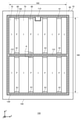
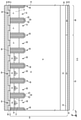
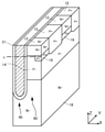
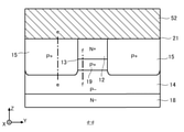
- FIG. 1 It is a top view which shows an example of the semiconductor device 100 which concerns on one Embodiment of this invention. It is an enlarged view of the area A in FIG. It is a figure which shows an example of the bb cross section in FIG. It is a perspective sectional view which shows an example of the mesa part 60. It is a figure which shows an example of the XY cross section of the mesa part 60 at the height position c shown in FIG. It is a figure which shows an example of the cross section in the dd line of FIG. It is a figure which shows the dd cross section in the comparative example. It is a figure which shows the other example of the dd cross section.
- one side in the direction parallel to the depth direction of the semiconductor substrate is referred to as "upper”, and the other side is referred to as “lower”.
- the upper surface is referred to as the upper surface and the other surface is referred to as the lower surface.
- the “up” and “down” directions are not limited to the direction of gravity or the direction when the semiconductor device is mounted.
- orthogonal coordinate axes of X-axis, Y-axis, and Z-axis Orthogonal axes only specify the relative positions of the components and do not limit a particular direction.
- the Z axis does not limit the height direction with respect to the ground.
- the + Z-axis direction and the ⁇ Z-axis direction are opposite to each other. When positive or negative is not described and is described as the Z-axis direction, it means the direction parallel to the + Z-axis and the -Z-axis.
- the orthogonal axes parallel to the upper surface and the lower surface of the semiconductor substrate are defined as the X axis and the Y axis. Further, the axis perpendicular to the upper surface and the lower surface of the semiconductor substrate is defined as the Z axis.
- the direction of the Z axis may be referred to as a depth direction. Further, in the present specification, the direction parallel to the upper surface and the lower surface of the semiconductor substrate including the X-axis and the Y-axis may be referred to as a horizontal direction.
- error When referred to as “same” or “equal” in the present specification, it may include a case where there is an error due to manufacturing variation or the like.
- the error is, for example, within 10%.
- the conductive type of the doping region doped with impurities is described as P-type or N-type.
- an impurity may mean, in particular, either an N-type donor or a P-type acceptor, and may be referred to as a dopant.
- doping means that a donor or acceptor is introduced into a semiconductor substrate to obtain a semiconductor showing an N-type conductive type or a semiconductor showing a P-type conductive type.
- P + type or N + type when described as P + type or N + type in the present specification, it means that the doping concentration is higher than that of P type or N type, and when described as P-type or N-type, it means that the doping concentration is higher than that of P type or N type. It means that the concentration is low. Further, when described as P ++ type or N ++ type in the present specification, it means that the doping concentration is higher than that of P + type or N + type.
- the donor concentration is sufficiently higher than the acceptor concentration, so the carrier concentration in the region may be used as the donor concentration.
- the carrier concentration in the region may be used as the acceptor concentration.
- the peak value may be used as the concentration of the donor, acceptor or doping in the region.
- the concentration of the donor, the acceptor or the doping is substantially uniform, the average value of the concentration of the donor, the acceptor or the doping in the region may be used as the concentration of the donor, the acceptor or the doping.
- FIG. 1 is a top view showing an example of a semiconductor device 100 according to an embodiment of the present invention.
- FIG. 1 shows a position where each member is projected onto the upper surface of the semiconductor substrate 10. In FIG. 1, only some members of the semiconductor device 100 are shown, and some members are omitted.
- the semiconductor device 100 includes a semiconductor substrate 10.
- the semiconductor substrate 10 has an end side 102 in a top view. When simply referred to as a top view in the present specification, it means that the semiconductor substrate 10 is viewed from the top surface side.
- the semiconductor substrate 10 of this example has two sets of end sides 102 facing each other in a top view. In FIG. 1, the X-axis and the Y-axis are parallel to either end 102. The Z-axis is perpendicular to the upper surface of the semiconductor substrate 10.
- the semiconductor substrate 10 is provided with an active portion 160.
- the active portion 160 is a region in which a main current flows in the depth direction between the upper surface and the lower surface of the semiconductor substrate 10 when the semiconductor device 100 operates.
- An emitter electrode is provided above the active portion 160, but it is omitted in FIG.
- the active unit 160 is provided with at least one of a transistor unit 70 including a transistor element such as an IGBT and a diode unit 80 including a diode element such as a freewheeling diode (FWD).
- a transistor unit 70 including a transistor element such as an IGBT and a diode unit 80 including a diode element such as a freewheeling diode (FWD).
- the transistor portion 70 and the diode portion 80 are alternately arranged along a predetermined arrangement direction (in this example, the X-axis direction) on the upper surface of the semiconductor substrate 10.
- the active portion 160 is not provided with the diode portion 80, but may be provided with the transistor portion 70.
- the symbol “I” is attached to the region where the transistor portion 70 is arranged, and the symbol “F” is attached to the region where the diode portion 80 is arranged.
- the direction perpendicular to the arrangement direction in top view may be referred to as a stretching direction (Y-axis direction in FIG. 1).
- the transistor portion 70 and the diode portion 80 may each have a longitudinal direction in the stretching direction. That is, the length of the transistor portion 70 in the Y-axis direction is larger than the width in the X-axis direction. Similarly, the length of the diode portion 80 in the Y-axis direction is larger than the width in the X-axis direction.
- the stretching direction of the transistor portion 70 and the diode portion 80 may be the same as the longitudinal direction of each trench portion described later.
- the diode portion 80 has an N + type cathode region in a region in contact with the lower surface of the semiconductor substrate 10.
- the region provided with the cathode region is referred to as a diode portion 80. That is, the diode portion 80 is a region that overlaps with the cathode region in the top view.
- a P + type collector region may be provided on the lower surface of the semiconductor substrate 10 in a region other than the cathode region.
- the diode portion 80 may also include an extension region 81 in which the diode portion 80 is extended in the Y-axis direction to the gate wiring described later.
- a collector area is provided on the lower surface of the extension area 81.
- the transistor portion 70 has a P + type collector region in a region in contact with the lower surface of the semiconductor substrate 10. Further, in the transistor portion 70, a gate structure having an N-type emitter region, a P-type base region, a gate conductive portion, and a gate insulating film is periodically arranged on the upper surface side of the semiconductor substrate 10.
- the semiconductor device 100 may have one or more pads above the semiconductor substrate 10.
- the semiconductor device 100 of this example has a gate pad 112.
- the semiconductor device 100 may have pads such as an anode pad, a cathode pad, and a current detection pad.
- Each pad is arranged in the vicinity of the end side 102.
- the vicinity of the end side 102 refers to a region between the end side 102 and the emitter electrode in top view.
- each pad may be connected to an external circuit via wiring such as a wire.
- a gate potential is applied to the gate pad 112.
- the gate pad 112 is electrically connected to the conductive portion of the gate trench portion of the active portion 160.
- the semiconductor device 100 includes a gate wiring that connects the gate pad 112 and the gate trench portion. In FIG. 1, diagonal hatching is attached to the gate wiring.
- the gate wiring of this example has an outer peripheral gate wiring 130 and an active side gate wiring 131.
- the outer peripheral gate wiring 130 is arranged between the active portion 160 and the end side 102 of the semiconductor substrate 10 in a top view.
- the outer peripheral gate wiring 130 of this example surrounds the active portion 160 in a top view.
- the region surrounded by the outer peripheral gate wiring 130 in the top view may be the active portion 160.
- the outer peripheral gate wiring 130 is connected to the gate pad 112.
- the outer peripheral gate wiring 130 is arranged above the semiconductor substrate 10.
- the outer peripheral gate wiring 130 may be a metal wiring containing aluminum or the like.
- the active side gate wiring 131 is provided in the active portion 160. By providing the active side gate wiring 131 in the active portion 160, it is possible to reduce variations in the wiring length from the gate pad 112 in each region of the semiconductor substrate 10.
- the active side gate wiring 131 is connected to the gate trench portion of the active portion 160.
- the active side gate wiring 131 is arranged above the semiconductor substrate 10.
- the active side gate wiring 131 may be wiring formed of a semiconductor such as polysilicon doped with impurities.
- the active side gate wiring 131 may be connected to the outer peripheral gate wiring 130.
- the active side gate wiring 131 of this example is provided extending from one outer peripheral gate wiring 130 to the other outer peripheral gate wiring 130 in the X-axis direction so as to cross the active portion 160 at substantially the center in the Y-axis direction. There is.
- the transistor portion 70 and the diode portion 80 may be alternately arranged in the X-axis direction in each divided region.
- the semiconductor device 100 of this example includes an edge termination structure portion 90 between the active portion 160 and the end side 102.
- the edge terminal structure portion 90 of this example is arranged between the outer peripheral gate wiring 130 and the end side 102.
- the edge termination structure 90 relaxes the electric field concentration on the upper surface side of the semiconductor substrate 10.
- the edge termination structure 90 may include at least one of a guard ring and a field plate provided in an annular shape surrounding the active portion 160.
- FIG. 2 is an enlarged view of the region A in FIG.
- the region A is a region including the transistor portion 70, the diode portion 80, and the active side gate wiring 131.
- the semiconductor device 100 of this example includes a gate trench portion 40, a dummy trench portion 30, a well region 11, an emitter region 12, a base region 14, and a contact region 15 provided inside the upper surface side of the semiconductor substrate 10.
- the gate trench portion 40 and the dummy trench portion 30 are examples of trench portions, respectively.
- the semiconductor device 100 of this example includes an emitter electrode 52 and an active side gate wiring 131 provided above the upper surface of the semiconductor substrate 10.
- the emitter electrode 52 and the active side gate wiring 131 are provided separately from each other.
- An interlayer insulating film is provided between the emitter electrode 52 and the active side gate wiring 131 and the upper surface of the semiconductor substrate 10, but this is omitted in FIG.
- the interlayer insulating film of this example is provided with a contact hole for connecting the emitter electrode 52, the active side gate wiring 131, and the semiconductor substrate 10.
- the emitter electrode 52 is provided above the gate trench portion 40, the dummy trench portion 30, the well region 11, the emitter region 12, the base region 14, and the contact region 15.
- the emitter electrode 52 comes into contact with the emitter region 12, the contact region 15, and the base region 14 on the upper surface of the semiconductor substrate 10. Further, the emitter electrode 52 is connected to the dummy conductive portion in the dummy trench portion 30.
- the active side gate wiring 131 is connected to the gate trench portion 40.
- the active side gate wiring 131 may be connected to the gate conductive portion of the gate trench portion 40 at the tip portion 41 of the gate trench portion 40 in the Y-axis direction.
- the active side gate wiring 131 is not connected to the dummy conductive portion in the dummy trench portion 30.
- the well region 11 is provided so as to overlap with the active side gate wiring 131.
- the well region 11 is extended to a predetermined width even in a range that does not overlap with the active side gate wiring 131.
- the well region 11 of this example is provided away from the end of the contact hole 54 in the Y-axis direction on the active side gate wiring 131 side.
- the well region 11 is a second conductive type region having a higher doping concentration than the base region 14.
- the base region 14 of this example is P-type, and the well region 11 is P + type.
- Each of the transistor portion 70 and the diode portion 80 has a plurality of trench portions arranged in the arrangement direction.
- the transistor portion 70 of this example one or more gate trench portions 40 and one or more dummy trench portions 30 are alternately provided along the arrangement direction.
- the diode portion 80 of this example is provided with a plurality of dummy trench portions 30 along the arrangement direction.
- the diode portion 80 of this example is not provided with the gate trench portion 40.
- the gate trench portion 40 of this example connects two straight line portions 39 (portion portions that are linear along the stretching direction) extending along a stretching direction perpendicular to the arrangement direction and two straight line portions 39. It may have a tip 41.
- the stretching direction in FIG. 2 is the Y-axis direction.
- the tip portion 41 is provided in a curved shape in a top view.
- the dummy trench portion 30 is provided between the straight line portions 39 of the gate trench portion 40.
- One dummy trench portion 30 may be provided between the straight line portions 39, and a plurality of dummy trench portions 30 may be provided.
- the dummy trench portion 30 may have a linear shape extending in the stretching direction, and may have a straight portion 29 and a tip portion 31 as in the gate trench portion 40.
- the diffusion depth of the well region 11 may be deeper than the depth of the gate trench portion 40 and the dummy trench portion 30.
- the ends of the gate trench portion 40 and the dummy trench portion 30 in the Y-axis direction are provided in the well region 11 in the top view. That is, at the end of each trench in the Y-axis direction, the bottom of each trench in the depth direction is covered with the well region 11. Thereby, the electric field concentration at the bottom of each trench can be relaxed.
- a mesa part is provided between each trench part in the arrangement direction.
- the mesa portion refers to a region sandwiched between trench portions inside the semiconductor substrate 10.
- the upper end of the mesa portion is the upper surface of the semiconductor substrate 10.
- the depth position of the lower end of the mesa portion is the same as the depth position of the lower end of the trench portion.
- the mesa portion of this example is provided on the upper surface of the semiconductor substrate 10 by extending in the stretching direction (Y-axis direction) along the trench.
- the transistor portion 70 is provided with a mesa portion 60
- the diode portion 80 is provided with a mesa portion 61.
- a mesa portion when simply referred to as a mesa portion in the present specification, it refers to each of the mesa portion 60 and the mesa portion 61.
- a base region 14 is provided in each mesa section. Of the base region 14 exposed on the upper surface of the semiconductor substrate 10 in the mesa portion, the region closest to the active side gate wiring 131 is referred to as the base region 14-e.
- FIG. 2 shows the base region 14-e arranged at one end of each mesa portion in the stretching direction, but the base region 14-e is also arranged at the other end portion of each mesa portion. Has been done.
- At least one of the first conductive type emitter region 12 and the second conductive type contact region 15 may be provided in each mesa portion in the region sandwiched between the base regions 14-e in the top view.
- the emitter region 12 of this example is N + type, and the contact region 15 is P + type.
- the emitter region 12 and the contact region 15 may be provided between the base region 14 and the upper surface of the semiconductor substrate 10 in the depth direction.
- the mesa portion 60 of the transistor portion 70 has an emitter region 12 and a contact region 15 exposed on the upper surface of the semiconductor substrate 10.
- Each of the emitter region 12 and the contact region 15 is in contact with both of the two trench portions sandwiching the mesa portion 60 on the upper surface of the semiconductor substrate 10. That is, each of the emitter region 12 and the contact region 15 is provided on the upper surface of the semiconductor substrate 10 over the entire width of the mesa portion 60 in the X-axis direction (arrangement direction). Further, the emitter region 12 and the contact region 15 are alternately arranged along the stretching direction (Y-axis direction).
- At least one mesa unit 60 has at least one connection area 19.
- the connection region 19 is provided in the mesa portion 60, which is the gate trench portion 40, at least one of the two trench portions sandwiching the mesa portion 60.
- the connection region 19 is a P + type region having a higher doping concentration than the base region 14.
- the connection region 19 is provided so as to overlap the emitter region 12 in the top view. However, the connection region 19 is arranged away from the gate trench portion 40 in the top view.
- connection region 19 is arranged below the upper surface of the semiconductor substrate 10 in the mesa portion 60.
- An emitter region 12 is provided between the connection region 19 and the upper surface of the semiconductor substrate 10.
- connection region 19 connects two contact regions 15 sandwiching the emitter region 12 in the Y-axis direction.
- the connection area 19 may be provided for each pair of two contact areas 15. That is, all the sets of the two contact regions 15 adjacent to each other in the Y-axis direction in the mesa portion 60 may be connected by the connection region 19. In FIG. 2, the range in which the connection area 19 is provided is shown by a broken line.
- the emitter region 12 is not provided in the mesa portion 61 of the diode portion 80.
- a base region 14 and a contact region 15 may be provided on the upper surface of the mesa portion 61.
- a contact region 15 may be provided in contact with the respective base regions 14-e in the region sandwiched between the base regions 14-e on the upper surface of the mesa portion 61.
- a base region 14 may be provided in a region sandwiched between the contact regions 15 on the upper surface of the mesa portion 61.
- the base region 14 may be arranged over the entire region sandwiched between the contact regions 15. Further, the mesa portion 61 is not provided with the connection area 19.
- Contact holes are provided in the interlayer insulating film that covers each mesa, but they are omitted in FIG.
- the contact hole is arranged in the region sandwiched between the base regions 14-e.
- the contact hole of this example is provided above each region of the contact region 15, the base region 14, and the emitter region 12.
- the contact hole may be arranged in the center in the arrangement direction (X-axis direction) of the mesa portion.
- an N + type cathode region 82 is provided in a region adjacent to the lower surface of the semiconductor substrate 10.
- a P + type collector region 22 may be provided on the lower surface of the semiconductor substrate 10 in a region where the cathode region 82 is not provided.
- FIG. 2 the boundary between the cathode region 82 and the collector region 22 is shown by a dotted line.
- FIG. 3 is a diagram showing an example of a bb cross section in FIG.
- the bb cross section is an XZ plane that passes through the emitter region 12 and the cathode region 82.
- the semiconductor device 100 of this example has a semiconductor substrate 10, an interlayer insulating film 38, an emitter electrode 52, and a collector electrode 24 in the cross section.
- the interlayer insulating film 38 is provided on the upper surface of the semiconductor substrate 10.
- the interlayer insulating film 38 is a film containing at least one layer of an insulating film such as silicate glass to which impurities such as boron and phosphorus are added, a thermal oxide film, and other insulating films.
- the interlayer insulating film 38 is provided with the contact hole 54 described with reference to FIG.
- the emitter electrode 52 is provided above the interlayer insulating film 38.
- the emitter electrode 52 is in contact with the upper surface 21 of the semiconductor substrate 10 through the contact hole 54 of the interlayer insulating film 38.
- the collector electrode 24 is provided on the lower surface 23 of the semiconductor substrate 10.
- the emitter electrode 52 and the collector electrode 24 are made of a metal material such as aluminum.
- the direction (Z-axis direction) connecting the emitter electrode 52 and the collector electrode 24 is referred to as a depth direction.
- the semiconductor substrate 10 has an N-type drift region 18.
- the drift region 18 is provided in each of the transistor portion 70 and the diode portion 80.
- the mesa portion 60 of the transistor portion 70 is provided with an N + type emitter region 12 and a P-type base region 14 in order from the upper surface 21 side of the semiconductor substrate 10.
- a drift region 18 is provided below the base region 14.
- the mesa portion 60 may be provided with an N + type storage region.
- the storage area is arranged between the base area 14 and the drift area 18.
- the emitter region 12 is exposed on the upper surface 21 of the semiconductor substrate 10 and is provided in contact with the gate trench portion 40.
- the emitter region 12 is in contact with the trench portions on both sides of the mesa portion 60.
- the emitter region 12 has a higher doping concentration than the drift region 18.
- the base region 14 is provided below the emitter region 12.
- the base region 14 of this example is provided in contact with the emitter region 12.
- the base region 14 is in contact with the trench portions on both sides of the mesa portion 60.
- connection region 19 overlaps with the emitter region 12 in top view. That is, the connection region 19 overlaps with the emitter region 12 in the Z-axis direction.
- the connection region 19 of this example is in contact with the lower end 13 of the emitter region 12.
- the lower end 13 of the emitter region 12 is the lowermost region of the emitter region 12.
- the mesa portion 61 of the diode portion 80 is provided with a P-type base region 14 in contact with the upper surface 21 of the semiconductor substrate 10.
- a drift region 18 is provided below the base region 14.
- an N + type buffer region 20 may be provided below the drift region 18.
- the doping concentration in the buffer region 20 is higher than the doping concentration in the drift region 18.
- the buffer region 20 may have a plurality of donor concentration peaks having a higher donor concentration than the drift region 18.
- the buffer region 20 may function as a field stop layer that prevents the depletion layer extending from the lower end of the base region 14 from reaching the P + type collector region 22 and the N + type cathode region 82.
- a P + type collector area 22 is provided below the buffer area 20.
- the acceptor concentration of the collector region 22 is higher than the acceptor concentration of the base region 14.
- the collector region 22 may include the same acceptors as the base region 14, or may include different acceptors.
- the acceptor of the collector region 22 is, for example, boron.
- an N + type cathode region 82 is provided below the buffer region 20.
- the donor concentration in the cathode region 82 is higher than the donor concentration in the drift region 18.
- the donor of the cathode region 82 is, for example, hydrogen or phosphorus.
- the elements that serve as donors and acceptors in each region are not limited to the above-mentioned examples.
- the collector region 22 and the cathode region 82 are exposed on the lower surface 23 of the semiconductor substrate 10 and are connected to the collector electrode 24.
- the collector electrode 24 may be in contact with the entire lower surface 23 of the semiconductor substrate 10.
- the collector electrode 24 is made of a metal material such as aluminum.
- One or more gate trench portions 40 and one or more dummy trench portions 30 are provided on the upper surface 21 side of the semiconductor substrate 10. Each trench portion penetrates the base region 14 from the upper surface 21 of the semiconductor substrate 10 and reaches the drift region 18. In the region where at least one of the emitter region 12 and the contact region 15 is provided, each trench portion also penetrates these doping regions and reaches the drift region 18. The fact that the trench portion penetrates the region is not limited to those manufactured in the order of forming the region and then forming the trench portion. Those in which the doping region is formed between the trench portions after the trench portion is formed are also included in those in which the trench portion penetrates the doping region.
- the transistor portion 70 is provided with a gate trench portion 40 and a dummy trench portion 30.
- the diode portion 80 is provided with a dummy trench portion 30 and is not provided with a gate trench portion 40.
- the boundary between the diode portion 80 and the transistor portion 70 in the X-axis direction is the boundary between the cathode region 82 and the collector region 22.
- the gate trench portion 40 has a gate trench, a gate insulating film 42, and a gate conductive portion 44 provided on the upper surface 21 of the semiconductor substrate 10.
- the gate insulating film 42 is provided so as to cover the inner wall of the gate trench.
- the gate insulating film 42 may be formed by oxidizing or nitriding the semiconductor on the inner wall of the gate trench.
- the gate conductive portion 44 is provided inside the gate trench inside the gate insulating film 42. That is, the gate insulating film 42 insulates the gate conductive portion 44 and the semiconductor substrate 10.
- the gate conductive portion 44 is formed of a conductive material such as polysilicon.
- the gate conductive portion 44 may be provided longer than the base region 14 in the depth direction.
- the gate trench portion 40 in the cross section is covered with the interlayer insulating film 38 on the upper surface 21 of the semiconductor substrate 10.
- the gate conductive portion 44 is electrically connected to the gate wiring. When a predetermined gate voltage is applied to the gate conductive portion 44, a channel due to an electron inversion layer is formed on the surface layer of the interface of the base region 14 in contact with the gate trench portion 40.
- connection area 19 is arranged away from the gate trench portion 40. As a result, fluctuations in the threshold voltage of the transistor unit 70 due to the provision of the connection region 19 can be suppressed.
- the boundary between the connection region 19 and the base region 14 in the X-axis direction may be a position where the doping concentration starts to increase in the direction from the trench portion toward the connection region 19.
- the P-type dopant in the connection region 19 and the P-type dopant in the base region 14 may be dopants of the same element. That is, the connection region 19 and the base region 14 may be formed by injecting a dopant of the same element. When a plurality of types of P-type dopants are contained in each region, the P-type dopant having the highest concentration in each region is used as the P-type dopant in the region.
- the P-type dopant in the connection region 19 and the P-type dopant in the base region 14 may be different. This makes it easier to control the shape of the connection area 19.
- the P-type dopant in the connection region 19 may be a dopant having a smaller diffusion coefficient in the semiconductor substrate 10 than the P-type dopant in the base region 14. That is, the P-type dopant in the connection region 19 may be a dopant that is less likely to diffuse in the semiconductor substrate 10 than the P-type dopant in the base region 14. As a result, the P-type dopant injected into the connection region 19 can be suppressed from diffusing to the gate trench portion 40, and the fluctuation of the threshold voltage can be suppressed.
- the dummy trench portion 30 may have the same structure as the gate trench portion 40 in the cross section.
- the dummy trench portion 30 has a dummy trench, a dummy insulating film 32, and a dummy conductive portion 34 provided on the upper surface 21 of the semiconductor substrate 10.
- the dummy conductive portion 34 may be electrically connected to the emitter electrode 52.
- the dummy insulating film 32 is provided so as to cover the inner wall of the dummy trench.
- the dummy conductive portion 34 is provided inside the dummy trench and inside the dummy insulating film 32.
- the dummy insulating film 32 insulates the dummy conductive portion 34 and the semiconductor substrate 10.
- the dummy conductive portion 34 may be formed of the same material as the gate conductive portion 44.
- the dummy conductive portion 34 is formed of a conductive material such as polysilicon.
- the dummy conductive portion 34 may have the same length as the gate conductive portion 44 in the depth direction
- FIG. 4 is a perspective sectional view showing an example of the mesa portion 60.
- FIG. 4 shows a YZ cross section and an XZ cross section that pass through the connection region 19 in the mesa portion 60.
- the connection region 19 connects two contact regions 15 sandwiching the emitter region 12 in the stretching direction (Y-axis direction). Further, the connection region 19 is arranged apart from the gate trench portion 40.
- FIG. 5 is a diagram showing an example of an XY cross section of the mesa portion 60 at the height position c shown in FIG.
- the cross section passes through the connecting region 19.
- the connection region 19 is sandwiched between the contact regions 15 in the Y-axis direction. Further, the connection region 19 of this example is sandwiched between the base regions 14 in the X-axis direction.
- connection region 19 is preferably arranged in the center between the two gate trenches 40 in the X-axis direction. That is, it is preferable that the distance between the connection region 19 and one gate trench portion 40 and the distance between the connection region 19 and the other gate trench portion 40 are the same. As a result, the connection region 19 can be easily separated from each of the two gate trench portions 40.
- one trench portion may be a dummy trench portion 30.
- the distance between the gate trench portion 40 and the connection region 19 in the X-axis direction may be 1 ⁇ m or more, 2 ⁇ m or more, or 3 ⁇ m or more.
- FIG. 6 is a diagram showing an example of a cross section on the dd line of FIG.
- the cross section is a YZ plane that passes through the connection region 19 in the mesa portion 60.
- the connection region 19 of this example is in contact with the lower end 13 of the emitter region 12.
- the transistor portion 70 of the semiconductor device 100 When the transistor portion 70 of the semiconductor device 100 is turned off, the holes existing in the drift region 18 and the like are extracted to the emitter electrode 52. By providing the high-concentration P-type contact region 15, the resistance in the hole movement path can be reduced and latch-up can be suppressed.
- connection region 19 the two contact regions 15 sandwiching the emitter region 12 can be connected by a high-concentration P-type region. Therefore, even when holes move between the two contact regions 15 at the time of turn-off for some reason, the resistance in the hole movement path can be reduced and latch-up can be suppressed.
- FIG. 7 is a diagram showing a dd cross section in a comparative example.
- the interlayer insulating film 38 remains at the time of patterning the interlayer insulating film 38, and one contact region 15-1 is covered with the interlayer insulating film 38.
- at least a part of the holes existing in the lower region of the contact region 15-1 moves to the contact region 15-1 at the time of turn-off.
- the holes in the contact region 15-1 cannot move to the emitter electrode 52, but move to the adjacent contact regions 15-2.
- connection area 19 is not provided. Therefore, the holes moving from the contact region 15-1 to the contact region 15-2 pass through the low-concentration base region 14.
- the hole movement path is schematically shown by a broken line arrow. In this case, the resistance in the hole movement path increases, and the voltage in the path rises. This can cause the parasitic npn transistor to turn on, causing latch-up failure.
- two adjacent contact regions 15 are connected by a high-concentration connection region 19. Therefore, holes can move between two adjacent contact regions 15 through the connection region 19, and the resistance of the hole movement path can be reduced. Therefore, latch-up can be suppressed.
- FIGS. 8A and 8B are diagrams showing other arrangement examples of the connection area 19.
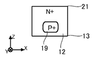
- FIG. 8A is a diagram showing another example of the dd cross section.
- FIG. 8B is a diagram showing an arrangement example of the emitter region 12 and the connection region 19 on the XZ plane.
- the depth position where the connection area 19 is arranged is different from the examples of FIGS. 1 to 6.
- Other structures are the same as any of the examples described in FIGS. 1-6.
- connection region 19 may be arranged inside the emitter region 12. That is, at least a part of the connection region 19 is sandwiched between the emitter regions 12 in the X-axis direction.
- the entire connection region 19 of this example is arranged inside the emitter region 12. For example, the entire connection region 19 is located above the lower end 13 of the emitter region 12. However, the connection region 19 is not in contact with the upper surface 21 of the semiconductor substrate 10.
- FIGS. 9A and 9B are diagrams showing other arrangement examples of the connection area 19.
- FIG. 9A is a diagram showing another example of the dd cross section.
- FIG. 9B is a diagram showing an arrangement example of the emitter region 12 and the connection region 19 on the XZ plane.
- the depth position where the connection area 19 is arranged is different from the examples of FIGS. 1 to 6.
- Other structures are the same as any of the examples described in FIGS. 1-6.
- a part of the region is arranged inside the emitter region 12, and a part of the region is arranged below the lower end 13 of the emitter region 12.
- FIGS. 10A and 10B are diagrams showing other arrangement examples of the connection area 19.
- FIG. 10A is a diagram showing another example of the dd cross section.
- FIG. 10B is a diagram showing an arrangement example of the emitter region 12 and the connection region 19 on the XZ plane.
- the depth position where the connection area 19 is arranged is different from the examples of FIGS. 1 to 6.
- Other structures are the same as any of the examples described in FIGS. 1-6.
- the connection region 19 of this example is arranged below the lower end 13 of the emitter region 12. That is, the connection region 19 is arranged apart from the emitter region 12.
- a base region 14 may be provided between the connection region 19 and the emitter region 12.
- FIG. 11 is a diagram showing an example of doping concentration distribution in the depth direction of the contact region 15 and the connection region 19.
- the doping concentration distribution of this example corresponds to the doping concentration distribution on the e-e line and the ff line shown in FIG.
- the doping concentration distribution of the contact region 15 is shown by a solid line
- the doping concentration distribution of the connection region 19 is shown by a broken line.
- the doping concentration distribution of the contact region 15 has a concentration peak 115
- the doping concentration distribution of the connection region 19 has a concentration peak 119.
- the doping concentration of the contact region 15 is P1, and the doping concentration of the connection region 19 is P2.
- the maximum doping concentration in each region may be the doping concentration in each region.
- the doping concentration P2 in the connection region 19 may be higher than the doping concentration P1 in the contact region 15. In this case, the resistance of the hole movement path between the contact regions 15 can be further reduced to suppress latch-up.
- the doping concentration P1 of the contact region 15 is made too high, the dopant of the contact region 15 may diffuse in the Y-axis direction, and the emitter region 12 may be shortened. According to this example, it becomes easy to suppress latch-up while ensuring the length of the emitter region 12.
- the doping concentration P2 of the connection region 19 may be 1 ⁇ 10 18 / cm 3 or more and 1 ⁇ 10 21 / cm 3 or less.
- the doping concentration P1 of the contact region 15 may be 10% or less of the doping concentration P2.
- the doping concentration P1 may be the same as the doping concentration P2 and may be higher than the doping concentration P2.
- the full width at half maximum of the concentration peak 115 in the contact region 15 is W1
- the full width at half maximum of the concentration peak 119 in the connection region 19 is W2.
- the full width at half maximum W2 may be smaller than the full width at half maximum W1.
- the full width at half maximum of the concentration peak can be adjusted by the heat treatment temperature after injecting the dopant, the heat treatment time, the type of dopant, and the like.
- the full width at half maximum W2 may be 50% or less of the full width at half maximum W1. According to this example, since the diffusion distance of the P-type dopant injected into the connection region 19 is small, it becomes easy to secure the distance between the connection region 19 and the gate trench portion 40.
- the position of the apex of each concentration peak is defined as the position of the concentration peak.
- the concentration peak 115 may be arranged on the upper surface 21 side of the semiconductor substrate 10 with respect to the concentration peak 119.
- the concentration peak 115 and the concentration peak 119 may be arranged at the same depth position, and the concentration peak 119 may be arranged on the upper surface 21 side of the concentration peak 115.
- FIG. 12 is a diagram showing another example of the XY cross section of the mesa portion 60 at the height position c shown in FIG.
- the position of the connection region 19 in the X-axis direction of the mesa portion 60 of this example is different from that of the example of FIG. Further, the mesa portion 60 of this example is sandwiched between the gate trench portion 40 and the dummy trench portion 30.
- Other structures are the same as in the example of FIG.
- connection area 19 of this example is arranged in the dummy trench portion 30 between the two trench portions. That is, the distance between the connection region 19 and the gate trench portion 40 in the X-axis direction is larger than the distance between the connection region 19 and the dummy trench portion 30 in the X-axis direction.
- the connection area 19 may be in contact with the dummy trench portion 30. As a result, the distance between the connection region 19 and the gate trench portion 40 can be increased. Therefore, the influence of the connection region 19 on the threshold voltage of the transistor unit 70 can be reduced.
- FIG. 13 is a diagram showing a part of the steps in the manufacturing method of the semiconductor device 100.
- the base region 14, each trench portion, each mesa portion, the emitter region 12 and the contact region 15 are formed on the semiconductor substrate 10 having the drift region 18.
- Each region can be formed by injecting a dopant into the semiconductor substrate 10 and heat-treating it.
- Each trench portion can be formed by selectively etching the upper surface 21 of the semiconductor substrate 10 to form a trench, and providing an insulating film and a conductive portion in the trench.
- the interlayer insulating film 38 and the contact hole 54 may be formed.
- connection area 19 is formed.
- the connection region 19 can be formed by selectively injecting a P-type dopant from the upper surface 21 of the mesa portion 60 and heat-treating it.
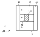
- FIG. 14 is a diagram showing an example of an injection region 140 into which a P-type dopant is injected in the second stage S1302.
- the injection region 140 is shown by hatching with diagonal lines. Areas other than the injection area 140 are masked with a resist or the like. In this example, the entire contact region 15 is masked, and a part of the emitter region 12 is masked. In addition, each trench portion is also masked. That is, the injection region 140 is a region in the same range as the connection region 19 described with reference to FIGS. 1 to 13 in the top view.
- the contact region 15 is masked and a high concentration P-type dopant is injected into the injection region 140. Therefore, it is possible to suppress fluctuations in the doping concentration distribution of the contact region 15 due to the formation of the connection region 19. Therefore, fluctuations in the characteristics of the semiconductor device 100 can be suppressed.
- FIG. 15 is a diagram showing another example of the injection region 140.
- the P-type dopant is injected into the region where the connection region 19 should be formed and at least a part of the region where the contact region 15 is formed. More specifically, the P-type dopant is also injected into a region of the contact region 15 that overlaps when the connection region 19 is extended in the Y-axis direction.
- the injection region 140 may cross the contact region 15 in the Y-axis direction and may be terminated in the contact region 15 in the Y-axis direction. According to this example, the connection area 19 and the contact area 15 can be reliably connected. Further, when the injection region 140 crosses the contact region 15, the masks do not have to be arranged discretely in the Y-axis direction, which facilitates manufacturing.
Landscapes
- Metal-Oxide And Bipolar Metal-Oxide Semiconductor Integrated Circuits (AREA)
- Electrodes Of Semiconductors (AREA)
Abstract
ドリフト領域と、ベース領域と、2つのトレンチ部と、メサ部とを有し、2つのトレンチ部の少なくとも一方はゲートトレンチ部であり、メサ部は、メサ部の上面に露出して設けられた第1導電型のエミッタ領域と、延伸方向において、エミッタ領域と交互にメサ部の上面に露出して設けられた第2導電型のコンタクト領域と、上面視においてエミッタ領域と重なって設けられ、ゲートトレンチ部と離れて配置され、メサ部の上面よりも下方に配置され、延伸方向においてエミッタ領域を挟む2つのコンタクト領域を接続する、ベース領域よりもドーピング濃度の高い第2導電型の接続領域とを有する半導体装置を提供する。
Description
本発明は、半導体装置および半導体装置の製造方法に関する。
従来、IGBT(絶縁ゲート型バイポーラトランジスタ)等の半導体装置が知られている(例えば、特許文献1-4参照)。
特許文献1 特開2019-195093号公報
特許文献2 特開2018-182279号公報
特許文献3 特開2008-34794号公報
特許文献4 WO2018/52098号
特許文献1 特開2019-195093号公報
特許文献2 特開2018-182279号公報
特許文献3 特開2008-34794号公報
特許文献4 WO2018/52098号
半導体装置のターンオフ時におけるラッチアップを抑制できることが好ましい。
上記課題を解決するために、本発明の一つの態様においては、半導体基板を備える半導体装置を提供する。半導体基板は、第1導電型のドリフト領域を有してよい。半導体基板は、ドリフト領域と半導体基板の上面との間に設けられた第2導電型のベース領域を有してよい。半導体基板は、半導体基板の上面において予め定められた延伸方向に延伸して設けられ、半導体基板の上面からドリフト領域まで設けられた2つのトレンチ部を有してよい。半導体基板は、2つのトレンチ部の間に設けられたメサ部を有してよい。2つのトレンチ部の少なくとも一方はゲートトレンチ部であってよい。メサ部は、メサ部の上面に露出して設けられ、2つのトレンチ部の両方と接して設けられた、ドリフト領域よりもドーピング濃度の高い第1導電型のエミッタ領域を有してよい。メサ部は、延伸方向において、エミッタ領域と交互にメサ部の上面に露出して設けられ、2つのトレンチ部の両方と接して設けられた第2導電型のコンタクト領域を有してよい。メサ部は、延伸方向においてエミッタ領域を挟む2つのコンタクト領域を接続する、ベース領域よりもドーピング濃度の高い第2導電型の接続領域を有してよい。接続領域は、上面視においてエミッタ領域と重なって設けられてよい。接続領域は、ゲートトレンチ部と離れて配置され、メサ部の上面よりも下方に配置されてよい。
接続領域は、エミッタ領域の下端と接していてよい。
接続領域の少なくとも一部は、エミッタ領域の内部に配置されていてよい。
接続領域は、エミッタ領域の下端よりも下方に配置されていてよい。
接続領域のドーピング濃度は、コンタクト領域のドーピング濃度よりも高くてよい。
接続領域は、コンタクト領域の第2導電型のドーパントとは異なる第2導電型のドーパントを含んでよい。
接続領域のドーパントは、コンタクト領域のドーパントよりも、半導体基板における拡散係数が高くてよい。
2つのトレンチ部は、両方ともゲートトレンチ部であってよい。接続領域は、2つのトレンチ部の間の中央に配置されていてよい。
2つのトレンチ部の一方はゲートトレンチ部、他方はダミートレンチ部であってよい。接続領域は、2つのトレンチ部の間において、ダミートレンチ部よりに配置されていてよい。
コンタクト領域および接続領域のそれぞれは、半導体基板の深さ方向においてドーピング濃度の濃度ピークを有してよい。コンタクト領域の濃度ピークは、接続領域の濃度ピークよりも半導体基板の上面側に配置されていてよい。
本発明の第二の態様においては、半導体装置の製造方法を提供する。製造方法は、第1段階および第2段階を備えてよい。第1段階では、第1導電型のドリフト領域を有する半導体基板に、ドリフト領域と半導体基板の上面との間に設けられた第2導電型のベース領域を形成してよい。第1段階では、半導体基板の上面において予め定められた延伸方向に延伸して設けられ、半導体基板の上面からドリフト領域まで設けられた2つのトレンチ部を形成してよい。第1段階では、2つのトレンチ部の間に設けられたメサ部を形成してよい。第1段階では、メサ部の上面に露出し、2つのトレンチ部の両方と接し、ドリフト領域よりもドーピング濃度の高い第1導電型のエミッタ領域を形成してよい。第1段階では、延伸方向において、エミッタ領域と交互にメサ部の上面に露出し、2つのトレンチ部の両方と接する第2導電型のコンタクト領域を形成してよい。第2段階では、延伸方向においてエミッタ領域を挟む2つのコンタクト領域を接続する、ベース領域よりもドーピング濃度の高い第2導電型の接続領域を形成してよい。接続領域は、上面視においてエミッタ領域と重なって設けられてよい。接続領域は、ゲートトレンチ部と離れて配置され、メサ部の上面よりも下方に配置されてよい。
第2段階において、コンタクト領域が形成された領域をマスクして、半導体基板に第2導電型のドーパントを注入することで、接続領域を形成してよい。
第2段階において、接続領域を形成すべき領域と、コンタクト領域が形成された領域の少なくとも一部の領域とに第2導電型のドーパントを注入することで、接続領域を形成してよい。
なお、上記の発明の概要は、本発明の必要な特徴の全てを列挙したものではない。また、これらの特徴群のサブコンビネーションもまた、発明となりうる。
以下、発明の実施の形態を通じて本発明を説明するが、以下の実施形態は請求の範囲にかかる発明を限定するものではない。また、実施形態の中で説明されている特徴の組み合わせの全てが発明の解決手段に必須であるとは限らない。
本明細書においては半導体基板の深さ方向と平行な方向における一方の側を「上」、他方の側を「下」と称する。基板、層またはその他の部材の2つの主面のうち、一方の面を上面、他方の面を下面と称する。「上」、「下」の方向は、重力方向または半導体装置の実装時における方向に限定されない。
本明細書では、X軸、Y軸およびZ軸の直交座標軸を用いて技術的事項を説明する場合がある。直交座標軸は、構成要素の相対位置を特定するに過ぎず、特定の方向を限定するものではない。例えば、Z軸は地面に対する高さ方向を限定して示すものではない。なお、+Z軸方向と-Z軸方向とは互いに逆向きの方向である。正負を記載せず、Z軸方向と記載した場合、+Z軸および-Z軸に平行な方向を意味する。
本明細書では、半導体基板の上面および下面に平行な直交軸をX軸およびY軸とする。また、半導体基板の上面および下面と垂直な軸をZ軸とする。本明細書では、Z軸の方向を深さ方向と称する場合がある。また、本明細書では、X軸およびY軸を含めて、半導体基板の上面および下面に平行な方向を、水平方向と称する場合がある。
本明細書において「同一」または「等しい」のように称した場合、製造ばらつき等に起因する誤差を有する場合も含んでよい。当該誤差は、例えば10%以内である。
本明細書においては、不純物がドーピングされたドーピング領域の導電型をP型またはN型として説明している。本明細書においては、不純物とは、特にN型のドナーまたはP型のアクセプタのいずれかを意味する場合があり、ドーパントと記載する場合がある。本明細書においては、ドーピングとは、半導体基板にドナーまたはアクセプタを導入し、N型の導電型を示す半導体またはP型の導電型を示す半導体とすることを意味する。
本明細書においてP+型またはN+型と記載した場合、P型またはN型よりもドーピング濃度が高いことを意味し、P-型またはN-型と記載した場合、P型またはN型よりもドーピング濃度が低いことを意味する。また、本明細書においてP++型またはN++型と記載した場合には、P+型またはN+型よりもドーピング濃度が高いことを意味する。
N型の領域においては、ドナー濃度がアクセプタ濃度よりも十分大きいので、当該領域におけるキャリア濃度を、ドナー濃度としてもよい。同様に、P型の領域においては、当該領域におけるキャリア濃度を、アクセプタ濃度としてもよい。
また、ドナー、アクセプタまたはドーピングの濃度分布がピークを有する場合、当該ピーク値を当該領域におけるドナー、アクセプタまたはドーピングの濃度としてよい。ドナー、アクセプタまたはドーピングの濃度がほぼ均一な場合等においては、当該領域におけるドナー、アクセプタまたはドーピングの濃度の平均値をドナー、アクセプタまたはドーピングの濃度としてよい。
図1は、本発明の一つの実施形態に係る半導体装置100の一例を示す上面図である。図1においては、各部材を半導体基板10の上面に投影した位置を示している。図1においては、半導体装置100の一部の部材だけを示しており、一部の部材は省略している。
半導体装置100は、半導体基板10を備えている。半導体基板10は、上面視において端辺102を有する。本明細書で単に上面視と称した場合、半導体基板10の上面側から見ることを意味している。本例の半導体基板10は、上面視において互いに向かい合う2組の端辺102を有する。図1においては、X軸およびY軸は、いずれかの端辺102と平行である。またZ軸は、半導体基板10の上面と垂直である。
半導体基板10には活性部160が設けられている。活性部160は、半導体装置100が動作した場合に半導体基板10の上面と下面との間で、深さ方向に主電流が流れる領域である。活性部160の上方には、エミッタ電極が設けられているが図1では省略している。
活性部160には、IGBT等のトランジスタ素子を含むトランジスタ部70と、還流ダイオード(FWD)等のダイオード素子を含むダイオード部80の少なくとも一方が設けられている。図1の例では、トランジスタ部70およびダイオード部80は、半導体基板10の上面における所定の配列方向(本例ではX軸方向)に沿って、交互に配置されている。他の例では、活性部160には、ダイオード部80が設けられておらず、トランジスタ部70が設けられていてもよい。
図1においては、トランジスタ部70が配置される領域には記号「I」を付し、ダイオード部80が配置される領域には記号「F」を付している。本明細書では、上面視において配列方向と垂直な方向を延伸方向(図1ではY軸方向)と称する場合がある。トランジスタ部70およびダイオード部80は、それぞれ延伸方向に長手を有してよい。つまり、トランジスタ部70のY軸方向における長さは、X軸方向における幅よりも大きい。同様に、ダイオード部80のY軸方向における長さは、X軸方向における幅よりも大きい。トランジスタ部70およびダイオード部80の延伸方向と、後述する各トレンチ部の長手方向とは同一であってよい。
ダイオード部80は、半導体基板10の下面と接する領域に、N+型のカソード領域を有する。本明細書では、カソード領域が設けられた領域を、ダイオード部80と称する。つまりダイオード部80は、上面視においてカソード領域と重なる領域である。半導体基板10の下面においてカソード領域以外の領域には、P+型のコレクタ領域が設けられてよい。本明細書では、ダイオード部80を、後述するゲート配線までY軸方向に延長した延長領域81も、ダイオード部80に含める場合がある。延長領域81の下面には、コレクタ領域が設けられている。
トランジスタ部70は、半導体基板10の下面と接する領域に、P+型のコレクタ領域を有する。また、トランジスタ部70は、半導体基板10の上面側に、N型のエミッタ領域、P型のベース領域、ゲート導電部およびゲート絶縁膜を有するゲート構造が周期的に配置されている。
半導体装置100は、半導体基板10の上方に1つ以上のパッドを有してよい。本例の半導体装置100は、ゲートパッド112を有している。半導体装置100は、アノードパッド、カソードパッドおよび電流検出パッド等のパッドを有してもよい。各パッドは、端辺102の近傍に配置されている。端辺102の近傍とは、上面視における端辺102と、エミッタ電極との間の領域を指す。半導体装置100の実装時において、各パッドは、ワイヤ等の配線を介して外部の回路に接続されてよい。
ゲートパッド112には、ゲート電位が印加される。ゲートパッド112は、活性部160のゲートトレンチ部の導電部に電気的に接続される。半導体装置100は、ゲートパッド112とゲートトレンチ部とを接続するゲート配線を備える。図1においては、ゲート配線に斜線のハッチングを付している。
本例のゲート配線は、外周ゲート配線130と、活性側ゲート配線131とを有している。外周ゲート配線130は、上面視において活性部160と半導体基板10の端辺102との間に配置されている。本例の外周ゲート配線130は、上面視において活性部160を囲んでいる。上面視において外周ゲート配線130に囲まれた領域を活性部160としてもよい。また、外周ゲート配線130は、ゲートパッド112と接続されている。外周ゲート配線130は、半導体基板10の上方に配置されている。外周ゲート配線130は、アルミニウム等を含む金属配線であってよい。
活性側ゲート配線131は、活性部160に設けられている。活性部160に活性側ゲート配線131を設けることで、半導体基板10の各領域について、ゲートパッド112からの配線長のばらつきを低減できる。
活性側ゲート配線131は、活性部160のゲートトレンチ部と接続される。活性側ゲート配線131は、半導体基板10の上方に配置されている。活性側ゲート配線131は、不純物がドープされたポリシリコン等の半導体で形成された配線であってよい。
活性側ゲート配線131は、外周ゲート配線130と接続されてよい。本例の活性側ゲート配線131は、一方の外周ゲート配線130から他方の外周ゲート配線130まで、Y軸方向の略中央で活性部160を横切るように、X軸方向に延伸して設けられている。活性側ゲート配線131により活性部160が分割されている場合、それぞれの分割領域において、トランジスタ部70およびダイオード部80がX軸方向に交互に配置されてよい。
本例の半導体装置100は、活性部160と端辺102との間に、エッジ終端構造部90を備える。本例のエッジ終端構造部90は、外周ゲート配線130と端辺102との間に配置されている。エッジ終端構造部90は、半導体基板10の上面側の電界集中を緩和する。エッジ終端構造部90は、活性部160を囲んで環状に設けられたガードリングおよびフィールドプレートのうちの少なくとも一つを備えていてよい。
図2は、図1における領域Aの拡大図である。領域Aは、トランジスタ部70、ダイオード部80、および、活性側ゲート配線131を含む領域である。本例の半導体装置100は、半導体基板10の上面側の内部に設けられたゲートトレンチ部40、ダミートレンチ部30、ウェル領域11、エミッタ領域12、ベース領域14およびコンタクト領域15を備える。ゲートトレンチ部40およびダミートレンチ部30は、それぞれがトレンチ部の一例である。また、本例の半導体装置100は、半導体基板10の上面の上方に設けられたエミッタ電極52および活性側ゲート配線131を備える。エミッタ電極52および活性側ゲート配線131は互いに分離して設けられる。
エミッタ電極52および活性側ゲート配線131と、半導体基板10の上面との間には層間絶縁膜が設けられるが、図1では省略している。本例の層間絶縁膜には、エミッタ電極52および活性側ゲート配線131と、半導体基板10とを接続するためのコンタクトホールが設けられる。
エミッタ電極52は、ゲートトレンチ部40、ダミートレンチ部30、ウェル領域11、エミッタ領域12、ベース領域14およびコンタクト領域15の上方に設けられる。エミッタ電極52は、半導体基板10の上面におけるエミッタ領域12、コンタクト領域15およびベース領域14と接触する。また、エミッタ電極52は、ダミートレンチ部30内のダミー導電部と接続される。
活性側ゲート配線131は、ゲートトレンチ部40と接続する。活性側ゲート配線131は、Y軸方向におけるゲートトレンチ部40の先端部41において、ゲートトレンチ部40のゲート導電部と接続されてよい。活性側ゲート配線131は、ダミートレンチ部30内のダミー導電部とは接続されない。
ウェル領域11は、活性側ゲート配線131と重なって設けられている。ウェル領域11は、活性側ゲート配線131と重ならない範囲にも、所定の幅で延伸して設けられている。本例のウェル領域11は、コンタクトホール54のY軸方向の端から、活性側ゲート配線131側に離れて設けられている。ウェル領域11は、ベース領域14よりもドーピング濃度の高い第2導電型の領域である。本例のベース領域14はP-型であり、ウェル領域11はP+型である。
トランジスタ部70およびダイオード部80のそれぞれは、配列方向に複数配列されたトレンチ部を有する。本例のトランジスタ部70には、配列方向に沿って1本以上のゲートトレンチ部40と、1本以上のダミートレンチ部30とが交互に設けられている。本例のダイオード部80には、複数のダミートレンチ部30が、配列方向に沿って設けられている。本例のダイオード部80には、ゲートトレンチ部40が設けられていない。
本例のゲートトレンチ部40は、配列方向と垂直な延伸方向に沿って延伸する2つの直線部分39(延伸方向に沿って直線状であるトレンチの部分)と、2つの直線部分39を接続する先端部41を有してよい。図2における延伸方向はY軸方向である。
先端部41の少なくとも一部は、上面視において曲線状に設けられることが好ましい。2つの直線部分39のY軸方向における端部どうしを先端部41が接続することで、直線部分39の端部における電界集中を緩和できる。
トランジスタ部70において、ダミートレンチ部30はゲートトレンチ部40のそれぞれの直線部分39の間に設けられる。それぞれの直線部分39の間には、1本のダミートレンチ部30が設けられてよく、複数本のダミートレンチ部30が設けられていてもよい。ダミートレンチ部30は、延伸方向に延伸する直線形状を有してよく、ゲートトレンチ部40と同様に、直線部分29と先端部31とを有していてもよい。
ウェル領域11の拡散深さは、ゲートトレンチ部40およびダミートレンチ部30の深さよりも深くてよい。ゲートトレンチ部40およびダミートレンチ部30のY軸方向の端部は、上面視においてウェル領域11に設けられる。つまり、各トレンチ部のY軸方向の端部において、各トレンチ部の深さ方向の底部は、ウェル領域11に覆われている。これにより、各トレンチ部の当該底部における電界集中を緩和できる。
配列方向において各トレンチ部の間には、メサ部が設けられている。メサ部は、半導体基板10の内部において、トレンチ部に挟まれた領域を指す。一例としてメサ部の上端は半導体基板10の上面である。メサ部の下端の深さ位置は、トレンチ部の下端の深さ位置と同一である。本例のメサ部は、半導体基板10の上面において、トレンチに沿って延伸方向(Y軸方向)に延伸して設けられている。本例では、トランジスタ部70にはメサ部60が設けられ、ダイオード部80にはメサ部61が設けられている。本明細書において単にメサ部と称した場合、メサ部60およびメサ部61のそれぞれを指している。
それぞれのメサ部には、ベース領域14が設けられる。メサ部において半導体基板10の上面に露出したベース領域14のうち、活性側ゲート配線131に最も近く配置された領域をベース領域14-eとする。図2においては、それぞれのメサ部の延伸方向における一方の端部に配置されたベース領域14-eを示しているが、それぞれのメサ部の他方の端部にもベース領域14-eが配置されている。それぞれのメサ部には、上面視においてベース領域14-eに挟まれた領域に、第1導電型のエミッタ領域12および第2導電型のコンタクト領域15の少なくとも一方が設けられてよい。本例のエミッタ領域12はN+型であり、コンタクト領域15はP+型である。エミッタ領域12およびコンタクト領域15は、深さ方向において、ベース領域14と半導体基板10の上面との間に設けられてよい。
トランジスタ部70のメサ部60は、半導体基板10の上面に露出したエミッタ領域12およびコンタクト領域15を有する。エミッタ領域12およびコンタクト領域15のそれぞれは、半導体基板10の上面において、メサ部60を挟む2つのトレンチ部の両方と接している。つまり、エミッタ領域12およびコンタクト領域15のそれぞれは、半導体基板10の上面において、X軸方向(配列方向)におけるメサ部60の全幅に渡って設けられている。また、エミッタ領域12およびコンタクト領域15のそれぞれは、延伸方向(Y軸方向)に沿って交互に配置されている。
少なくとも一つのメサ部60は、少なくとも一つの接続領域19を有する。接続領域19は、メサ部60を挟む2つのトレンチ部のうち、少なくとも一つのトレンチ部がゲートトレンチ部40であるメサ部60に設けられている。接続領域19は、ベース領域14よりもドーピング濃度の高いP+型の領域である。接続領域19は、上面視においてエミッタ領域12と重なって設けられている。ただし接続領域19は、上面視においてゲートトレンチ部40と離れて配置されている。
また、接続領域19は、メサ部60における半導体基板10の上面よりも下方に配置されている。接続領域19と半導体基板10の上面との間には、エミッタ領域12が設けられている。
接続領域19は、Y軸方向においてエミッタ領域12を挟む2つのコンタクト領域15を接続する。接続領域19は、2つのコンタクト領域15の組毎に設けられてよい。つまり、メサ部60においてY軸方向において隣り合う2つのコンタクト領域15の全てのセットが、接続領域19により接続されてよい。図2においては、接続領域19が設けられている範囲を破線で示している。接続領域19を設けることで、後述するように、ターンオフ時における半導体装置100のラッチアップを抑制できる。
ダイオード部80のメサ部61には、エミッタ領域12が設けられていない。メサ部61の上面には、ベース領域14およびコンタクト領域15が設けられてよい。メサ部61の上面においてベース領域14-eに挟まれた領域には、それぞれのベース領域14-eに接してコンタクト領域15が設けられてよい。メサ部61の上面においてコンタクト領域15に挟まれた領域には、ベース領域14が設けられてよい。ベース領域14は、コンタクト領域15に挟まれた領域全体に配置されてよい。また、メサ部61には、接続領域19が設けられていない。
それぞれのメサ部を覆う層間絶縁膜には、コンタクトホールが設けられているが、図2では省略している。コンタクトホールは、ベース領域14-eに挟まれた領域に配置されている。本例のコンタクトホールは、コンタクト領域15、ベース領域14およびエミッタ領域12の各領域の上方に設けられる。コンタクトホールは、メサ部の配列方向(X軸方向)における中央に配置されてよい。
ダイオード部80において、半導体基板10の下面と隣接する領域には、N+型のカソード領域82が設けられる。半導体基板10の下面において、カソード領域82が設けられていない領域には、P+型のコレクタ領域22が設けられてよい。図2においては、カソード領域82およびコレクタ領域22の境界を点線で示している。
図3は、図2におけるb-b断面の一例を示す図である。b-b断面は、エミッタ領域12およびカソード領域82を通過するXZ面である。本例の半導体装置100は、当該断面において、半導体基板10、層間絶縁膜38、エミッタ電極52およびコレクタ電極24を有する。層間絶縁膜38は、半導体基板10の上面に設けられている。層間絶縁膜38は、ホウ素またはリン等の不純物が添加されたシリケートガラス等の絶縁膜、熱酸化膜、および、その他の絶縁膜の少なくとも一層を含む膜である。層間絶縁膜38には、図2において説明したコンタクトホール54が設けられている。
エミッタ電極52は、層間絶縁膜38の上方に設けられる。エミッタ電極52は、層間絶縁膜38のコンタクトホール54を通って、半導体基板10の上面21と接触している。コレクタ電極24は、半導体基板10の下面23に設けられる。エミッタ電極52およびコレクタ電極24は、アルミニウム等の金属材料で形成されている。本明細書において、エミッタ電極52とコレクタ電極24とを結ぶ方向(Z軸方向)を深さ方向と称する。
半導体基板10は、N-型のドリフト領域18を有する。ドリフト領域18は、トランジスタ部70およびダイオード部80のそれぞれに設けられている。
トランジスタ部70のメサ部60には、N+型のエミッタ領域12およびP-型のベース領域14が、半導体基板10の上面21側から順番に設けられている。ベース領域14の下方にはドリフト領域18が設けられている。メサ部60には、N+型の蓄積領域が設けられてもよい。蓄積領域は、ベース領域14とドリフト領域18との間に配置される。ドリフト領域18とベース領域14との間に高濃度の蓄積領域を設けることで、キャリア注入促進効果(IE効果)を高めて、オン電圧を低減できる。
エミッタ領域12は半導体基板10の上面21に露出しており、且つ、ゲートトレンチ部40と接して設けられている。エミッタ領域12は、メサ部60の両側のトレンチ部と接している。エミッタ領域12は、ドリフト領域18よりもドーピング濃度が高い。
ベース領域14は、エミッタ領域12の下方に設けられている。本例のベース領域14は、エミッタ領域12と接して設けられている。ベース領域14は、メサ部60の両側のトレンチ部と接している。
メサ部60には、接続領域19が設けられている。上述したように、接続領域19は、上面視においてエミッタ領域12と重なっている。つまり、接続領域19は、エミッタ領域12とZ軸方向において重なっている。本例の接続領域19は、エミッタ領域12の下端13と接している。エミッタ領域12の下端13は、エミッタ領域12において最も下方に設けられた領域である。
ダイオード部80のメサ部61には、半導体基板10の上面21に接して、P-型のベース領域14が設けられている。ベース領域14の下方には、ドリフト領域18が設けられている。
トランジスタ部70およびダイオード部80のそれぞれにおいて、ドリフト領域18の下にはN+型のバッファ領域20が設けられてよい。バッファ領域20のドーピング濃度は、ドリフト領域18のドーピング濃度よりも高い。バッファ領域20は、ドリフト領域18よりもドナー濃度の高い複数のドナー濃度ピークを有してよい。バッファ領域20は、ベース領域14の下端から広がる空乏層が、P+型のコレクタ領域22およびN+型のカソード領域82に到達することを防ぐフィールドストップ層として機能してよい。
トランジスタ部70において、バッファ領域20の下には、P+型のコレクタ領域22が設けられる。コレクタ領域22のアクセプタ濃度は、ベース領域14のアクセプタ濃度より高い。コレクタ領域22は、ベース領域14と同一のアクセプタを含んでよく、異なるアクセプタを含んでもよい。コレクタ領域22のアクセプタは、例えばボロンである。
ダイオード部80において、バッファ領域20の下には、N+型のカソード領域82が設けられる。カソード領域82のドナー濃度は、ドリフト領域18のドナー濃度より高い。カソード領域82のドナーは、例えば水素またはリンである。なお、各領域のドナーおよびアクセプタとなる元素は、上述した例に限定されない。コレクタ領域22およびカソード領域82は、半導体基板10の下面23に露出しており、コレクタ電極24と接続している。コレクタ電極24は、半導体基板10の下面23全体と接触してよい。コレクタ電極24は、アルミニウム等の金属材料で形成される。
半導体基板10の上面21側には、1つ以上のゲートトレンチ部40、および、1つ以上のダミートレンチ部30が設けられる。各トレンチ部は、半導体基板10の上面21から、ベース領域14を貫通して、ドリフト領域18に到達している。エミッタ領域12およびコンタクト領域15の少なくとも一方が設けられている領域においては、各トレンチ部はこれらのドーピング領域も貫通して、ドリフト領域18に到達している。トレンチ部が領域を貫通するとは、領域を形成してからトレンチ部を形成する順序で製造したものに限定されない。トレンチ部を形成した後に、トレンチ部の間にドーピング領域を形成したものも、トレンチ部がドーピング領域を貫通しているものに含まれる。
上述したように、トランジスタ部70には、ゲートトレンチ部40およびダミートレンチ部30が設けられている。ダイオード部80には、ダミートレンチ部30が設けられ、ゲートトレンチ部40が設けられていない。本例においてダイオード部80とトランジスタ部70のX軸方向における境界は、カソード領域82とコレクタ領域22の境界である。
ゲートトレンチ部40は、半導体基板10の上面21に設けられたゲートトレンチ、ゲート絶縁膜42およびゲート導電部44を有する。ゲート絶縁膜42は、ゲートトレンチの内壁を覆って設けられる。ゲート絶縁膜42は、ゲートトレンチの内壁の半導体を酸化または窒化して形成してよい。ゲート導電部44は、ゲートトレンチの内部においてゲート絶縁膜42よりも内側に設けられる。つまりゲート絶縁膜42は、ゲート導電部44と半導体基板10とを絶縁する。ゲート導電部44は、ポリシリコン等の導電材料で形成される。
ゲート導電部44は、深さ方向において、ベース領域14よりも長く設けられてよい。当該断面におけるゲートトレンチ部40は、半導体基板10の上面21において層間絶縁膜38により覆われる。ゲート導電部44は、ゲート配線に電気的に接続されている。ゲート導電部44に所定のゲート電圧が印加されると、ベース領域14のうちゲートトレンチ部40に接する界面の表層に電子の反転層によるチャネルが形成される。
接続領域19は、ゲートトレンチ部40から離れて配置されている。これにより、接続領域19を設けたことによる、トランジスタ部70の閾値電圧の変動を抑制できる。X軸方向における接続領域19とベース領域14との境界は、トレンチ部から接続領域19に向かう方向において、ドーピング濃度が上昇し始める位置であってよい。
接続領域19におけるP型ドーパントと、ベース領域14におけるP型ドーパントは、同一元素のドーパントであってよい。つまり、接続領域19とベース領域14は、同一元素のドーパントを注入することで形成されてよい。なお、各領域に複数種類のP型ドーパントが含まれている場合、各領域において最も高濃度のP型ドーパントを、当該領域におけるP型ドーパントとする。
他の例では、接続領域19のP型ドーパントと、ベース領域14のP型ドーパントは、異なっていてもよい。これにより、接続領域19の形状を制御しやすくなる。
接続領域19におけるP型ドーパントは、ベース領域14におけるP型ドーパントよりも、半導体基板10における拡散係数が小さいドーパントであってよい。つまり、接続領域19におけるP型ドーパントは、ベース領域14におけるP型ドーパントよりも、半導体基板10において拡散しにくいドーパントであってよい。これにより、接続領域19に注入したP型ドーパントがゲートトレンチ部40まで拡散することを抑制でき、閾値電圧の変動を抑制できる。
ダミートレンチ部30は、当該断面において、ゲートトレンチ部40と同一の構造を有してよい。ダミートレンチ部30は、半導体基板10の上面21に設けられたダミートレンチ、ダミー絶縁膜32およびダミー導電部34を有する。ダミー導電部34は、エミッタ電極52に電気的に接続してよい。ダミー絶縁膜32は、ダミートレンチの内壁を覆って設けられる。ダミー導電部34は、ダミートレンチの内部に設けられ、且つ、ダミー絶縁膜32よりも内側に設けられる。ダミー絶縁膜32は、ダミー導電部34と半導体基板10とを絶縁する。ダミー導電部34は、ゲート導電部44と同一の材料で形成されてよい。例えばダミー導電部34は、ポリシリコン等の導電材料で形成される。ダミー導電部34は、深さ方向においてゲート導電部44と同一の長さを有してよい。
図4は、メサ部60の一例を示す斜視断面図である。図4においては、メサ部60において接続領域19を通過するYZ断面およびXZ断面を示している。上述したように、接続領域19は、延伸方向(Y軸方向)においてエミッタ領域12を挟む2つのコンタクト領域15を接続する。また、接続領域19は、ゲートトレンチ部40とは離れて配置されている。
図5は、図4に示した高さ位置cにおけるメサ部60のXY断面の一例を示す図である。当該断面は、接続領域19を通過する。接続領域19は、Y軸方向においてコンタクト領域15に挟まれている。また、本例の接続領域19は、X軸方向においてベース領域14に挟まれている。
図5に示すメサ部60は、2つのゲートトレンチ部40に挟まれている。この場合、接続領域19は、X軸方向において、2つのゲートトレンチ部40の間の中央に配置されることが好ましい。つまり、接続領域19と一方のゲートトレンチ部40との距離と、接続領域19ともう一方のゲートトレンチ部40との距離が同一であることが好ましい。これにより、2つのゲートトレンチ部40のそれぞれに対して、接続領域19を離間させやすくなる。他の例では、一方のトレンチ部がダミートレンチ部30であってもよい。ゲートトレンチ部40と接続領域19のX軸方向の距離は、1μm以上であってよく、2μm以上であってよく、3μm以上であってもよい。
図6は、図5のd-d線における断面の一例を示す図である。当該断面は、メサ部60において接続領域19を通過するYZ面である。本例の接続領域19は、エミッタ領域12の下端13と接している。
半導体装置100のトランジスタ部70をターンオフさせると、ドリフト領域18等に存在していた正孔がエミッタ電極52に引き抜かれる。高濃度のP型のコンタクト領域15を設けることで、正孔の移動経路における抵抗を小さくして、ラッチアップを抑制できる。
さらに接続領域19を設けることで、エミッタ領域12を挟む2つのコンタクト領域15を、高濃度のP型領域で接続できる。このため、何らかの要因で、ターンオフ時に2つのコンタクト領域15間を正孔が移動する場合であっても、正孔の移動経路における抵抗を小さくして、ラッチアップを抑制できる。
図7は、比較例におけるd-d断面を示す図である。本例においては、層間絶縁膜38のパターニング時に層間絶縁膜38が残存して、一つのコンタクト領域15-1が層間絶縁膜38に覆われている。この場合、コンタクト領域15-1の下方の領域に存在していた正孔の少なくとも一部は、ターンオフ時にコンタクト領域15-1に移動する。しかし、コンタクト領域15-1は層間絶縁膜38に覆われているので、コンタクト領域15-1の正孔はエミッタ電極52に移動できずに、隣り合うコンタクト領域15-2に移動する。
比較例においては、接続領域19が設けられていない。このため、コンタクト領域15-1からコンタクト領域15-2に移動する正孔は、低濃度のベース領域14を通過する。図7においては、正孔の移動経路を、破線の矢印で模式的に示している。この場合、正孔の移動経路における抵抗が高くなり、当該経路における電圧が上昇する。これにより、寄生npnトランジスタがターンオンして、ラッチアップ破壊が引き起こされる場合がある。
これに対して図1から図6において説明した例では、隣り合う2つのコンタクト領域15が高濃度の接続領域19で接続されている。このため、隣り合う2つのコンタクト領域15間を、接続領域19を通って正孔が移動でき、正孔の移動経路を低抵抗化できる。従って、ラッチアップを抑制できる。
図8Aおよび図8Bは、接続領域19の他の配置例を示す図である。図8Aは、d-d断面の他の例を示す図である。図8Bは、XZ面におけるエミッタ領域12と接続領域19の配置例を示す図である。本例では、接続領域19が配置された深さ位置が、図1から図6の例と相違する。他の構造は、図1から図6において説明したいずれかの例と同一である。
接続領域19は、少なくとも一部が、エミッタ領域12の内部に配置されてよい。つまり、接続領域19の少なくとも一部の領域が、X軸方向においてエミッタ領域12に挟まれている。本例の接続領域19は、全体が、エミッタ領域12の内部に配置されている。例えば、接続領域19の全体が、エミッタ領域12の下端13よりも上方に配置される。ただし、接続領域19は、半導体基板10の上面21には接していない。
図9Aおよび図9Bは、接続領域19の他の配置例を示す図である。図9Aは、d-d断面の他の例を示す図である。図9Bは、XZ面におけるエミッタ領域12と接続領域19の配置例を示す図である。本例では、接続領域19が配置された深さ位置が、図1から図6の例と相違する。他の構造は、図1から図6において説明したいずれかの例と同一である。本例の接続領域19は、一部の領域がエミッタ領域12の内部に配置され、一部の領域がエミッタ領域12の下端13よりも下方に配置されている。
図10Aおよび図10Bは、接続領域19の他の配置例を示す図である。図10Aは、d-d断面の他の例を示す図である。図10Bは、XZ面におけるエミッタ領域12と接続領域19の配置例を示す図である。本例では、接続領域19が配置された深さ位置が、図1から図6の例と相違する。他の構造は、図1から図6において説明したいずれかの例と同一である。本例の接続領域19は、エミッタ領域12の下端13よりも下方に配置されている。つまり接続領域19は、エミッタ領域12と離れて配置されている。接続領域19およびエミッタ領域12の間には、ベース領域14が設けられてよい。
図11は、コンタクト領域15および接続領域19の深さ方向におけるドーピング濃度分布例を示す図である。本例のドーピング濃度分布は、図6に示すe-e線およびf-f線におけるドーピング濃度分布に対応する。図11では、コンタクト領域15のドーピング濃度分布を実線で示し、接続領域19のドーピング濃度分布を破線で示している。コンタクト領域15のドーピング濃度分布は濃度ピーク115を有し、接続領域19のドーピング濃度分布は濃度ピーク119を有する。
コンタクト領域15のドーピング濃度をP1とし、接続領域19のドーピング濃度をP2とする。各領域の最大ドーピング濃度を、各領域のドーピング濃度としてよい。接続領域19のドーピング濃度P2は、コンタクト領域15のドーピング濃度P1よりも高くてよい。この場合、コンタクト領域15間の正孔の移動経路を更に低抵抗化して、ラッチアップを抑制できる。
また、コンタクト領域15のドーピング濃度P1を高くしすぎると、コンタクト領域15のドーパントがY軸方向に拡散して、エミッタ領域12が短くなる場合がある。本例によれば、エミッタ領域12の長さを確保しつつ、ラッチアップを抑制しやすくなる。
接続領域19のドーピング濃度P2は、1×10¹⁸/cm3以上、1×1021/cm3以下であってよい。コンタクト領域15のドーピング濃度P1は、ドーピング濃度P2の10%以下であってよい。他の例では、ドーピング濃度P1は、ドーピング濃度P2と同一であってよく、ドーピング濃度P2より大きくてもよい。
また、コンタクト領域15の濃度ピーク115の半値全幅をW1とし、接続領域19の濃度ピーク119の半値全幅をW2とする。半値全幅W2は、半値全幅W1より小さくてよい。濃度ピークの半値全幅は、ドーパントを注入した後の熱処理温度、熱処理時間、または、ドーパントの種類等で調整できる。半値全幅W2は、半値全幅W1の50%以下であってよい。本例によれば、接続領域19に注入したP型ドーパントの拡散距離が小さいので、接続領域19とゲートトレンチ部40との距離を確保しやすくなる。
また、各濃度ピークの頂点の位置を、濃度ピークの位置とする。濃度ピーク115は、濃度ピーク119よりも半導体基板10の上面21側に配置されてよい。濃度ピーク115と濃度ピーク119は、同一の深さ位置に配置されてよく、濃度ピーク119が濃度ピーク115よりも上面21側に配置されてもよい。
図12は、図4に示した高さ位置cにおけるメサ部60のXY断面の他の例を示す図である。本例のメサ部60は、接続領域19のX軸方向における位置が、図4の例と相違する。また、本例のメサ部60は、ゲートトレンチ部40とダミートレンチ部30に挟まれている。他の構造は、図4の例と同一である。
本例の接続領域19は、2つのトレンチ部の間において、ダミートレンチ部30よりに配置されている。つまり、接続領域19とゲートトレンチ部40のX軸方向における距離は、接続領域19とダミートレンチ部30のX軸方向における距離よりも大きい。接続領域19は、ダミートレンチ部30と接していてもよい。これにより、接続領域19とゲートトレンチ部40との距離を大きくできる。このため、接続領域19を設けたことによる、トランジスタ部70の閾値電圧への影響を小さくできる。
図13は、半導体装置100の製造方法における一部の工程を示す図である。まず、第1段階S1301において、ドリフト領域18を有する半導体基板10に、ベース領域14、各トレンチ部、各メサ部、エミッタ領域12およびコンタクト領域15を形成する。各領域は、半導体基板10にドーパントを注入して熱処理することで形成できる。各トレンチ部は、半導体基板10の上面21を選択的にエッチングすることでトレンチを形成し、トレンチ内に絶縁膜および導電部を設けることで形成できる。第1段階S1301においては、層間絶縁膜38およびコンタクトホール54を形成してもよい。
次に第2段階S1302において、接続領域19を形成する。接続領域19は、メサ部60の上面21から、P型のドーパントを選択的に注入して熱処理することで形成できる。
図14は、第2段階S1302において、P型のドーパントを注入する注入領域140の一例を示す図である。図14において注入領域140を、斜線のハッチングで示している。注入領域140以外の領域は、レジスト等によりマスクされる。本例では、コンタクト領域15の全体をマスクし、また、エミッタ領域12の一部をマスクしている。また、各トレンチ部もマスクされる。つまり、注入領域140は、図1から図13において説明した接続領域19と、上面視において同一範囲の領域である。
本例によれば、コンタクト領域15をマスクして、高濃度のP型ドーパントを注入領域140に注入する。このため、接続領域19を形成することによる、コンタクト領域15のドーピング濃度分布の変動を抑制できる。従って半導体装置100の特性変動を抑制できる。
図15は、注入領域140の他の例を示す図である。本例では、接続領域19を形成すべき領域と、コンタクト領域15が形成された領域の少なくとも一部の領域とに、P型のドーパントを注入する。より具体的には、コンタクト領域15のうち、接続領域19をY軸方向に延長した場合に重なる領域にも、P型のドーパントを注入する。注入領域140は、コンタクト領域15をY軸方向に横断してよく、コンタクト領域15内でY軸方向に終端していてもよい。本例によれば、接続領域19とコンタクト領域15とを確実に接続できる。また、注入領域140がコンタクト領域15を横断している場合には、Y軸方向において離散的にマスクを配置しなくてよいので、製造が容易になる。
以上、本発明を実施の形態を用いて説明したが、本発明の技術的範囲は上記実施の形態に記載の範囲には限定されない。上記実施の形態に、多様な変更または改良を加えることが可能であることが当業者に明らかである。その様な変更または改良を加えた形態も本発明の技術的範囲に含まれ得ることが、請求の範囲の記載から明らかである。
請求の範囲、明細書、および図面中において示した装置、システム、プログラム、および方法における動作、手順、ステップ、および段階等の各処理の実行順序は、特段「より前に」、「先立って」等と明示しておらず、また、前の処理の出力を後の処理で用いるのでない限り、任意の順序で実現しうることに留意すべきである。請求の範囲、明細書、および図面中の動作フローに関して、便宜上「まず、」、「次に、」等を用いて説明したとしても、この順で実施することが必須であることを意味するものではない。
10・・・半導体基板、11・・・ウェル領域、12・・・エミッタ領域、13・・・下端、14・・・ベース領域、15・・・コンタクト領域、18・・・ドリフト領域、19・・・接続領域、20・・・バッファ領域、21・・・上面、22・・・コレクタ領域、23・・・下面、24・・・コレクタ電極、29・・・直線部分、30・・・ダミートレンチ部、31・・・先端部、32・・・ダミー絶縁膜、34・・・ダミー導電部、38・・・層間絶縁膜、39・・・直線部分、40・・・ゲートトレンチ部、41・・・先端部、42・・・ゲート絶縁膜、44・・・ゲート導電部、52・・・エミッタ電極、54・・・コンタクトホール、60、61・・・メサ部、70・・・トランジスタ部、80・・・ダイオード部、81・・・延長領域、82・・・カソード領域、90・・・エッジ終端構造部、100・・・半導体装置、102・・・端辺、112・・・ゲートパッド、115・・・濃度ピーク、119・・・濃度ピーク、130・・・外周ゲート配線、131・・・活性側ゲート配線、140・・・注入領域、160・・・活性部
Claims (13)
- 半導体基板を備える半導体装置であって、
前記半導体基板は、
第1導電型のドリフト領域と、
前記ドリフト領域と前記半導体基板の上面との間に設けられた第2導電型のベース領域と、
前記半導体基板の上面において予め定められた延伸方向に延伸して設けられ、前記半導体基板の上面から前記ドリフト領域まで設けられた2つのトレンチ部と、
前記2つのトレンチ部の間に設けられたメサ部と
を有し、
前記2つのトレンチ部の少なくとも一方はゲートトレンチ部であり、
前記メサ部は、
前記メサ部の上面に露出して設けられ、前記2つのトレンチ部の両方と接して設けられた、前記ドリフト領域よりもドーピング濃度の高い第1導電型のエミッタ領域と、
前記延伸方向において、前記エミッタ領域と交互に前記メサ部の上面に露出して設けられ、前記2つのトレンチ部の両方と接して設けられた第2導電型のコンタクト領域と、
上面視において前記エミッタ領域と重なって設けられ、前記ゲートトレンチ部と離れて配置され、前記メサ部の上面よりも下方に配置され、前記延伸方向において前記エミッタ領域を挟む2つの前記コンタクト領域を接続する、前記ベース領域よりもドーピング濃度の高い第2導電型の接続領域と
を有する半導体装置。 - 前記接続領域は、前記エミッタ領域の下端と接している
請求項1に記載の半導体装置。 - 前記接続領域の少なくとも一部は、前記エミッタ領域の内部に配置されている
請求項1に記載の半導体装置。 - 前記接続領域は、前記エミッタ領域の下端よりも下方に配置されている
請求項1に記載の半導体装置。 - 前記接続領域のドーピング濃度は、前記コンタクト領域のドーピング濃度よりも高い
請求項1から4のいずれか一項に記載の半導体装置。 - 前記接続領域は、前記コンタクト領域の第2導電型のドーパントとは異なる第2導電型のドーパントを含む
請求項1から5のいずれか一項に記載の半導体装置。 - 前記接続領域の前記ドーパントは、前記コンタクト領域の前記ドーパントよりも、前記半導体基板における拡散係数が高い
請求項6に記載の半導体装置。 - 前記2つのトレンチ部は、両方とも前記ゲートトレンチ部であり、
前記接続領域は、前記2つのトレンチ部の間の中央に配置されている
請求項1から7のいずれか一項に記載の半導体装置。 - 前記2つのトレンチ部の一方は前記ゲートトレンチ部、他方はダミートレンチ部であり、
前記接続領域は、前記2つのトレンチ部の間において、前記ダミートレンチ部よりに配置されている
請求項1から7のいずれか一項に記載の半導体装置。 - 前記コンタクト領域および前記接続領域のそれぞれは、前記半導体基板の深さ方向においてドーピング濃度の濃度ピークを有し、
前記コンタクト領域の前記濃度ピークは、前記接続領域の前記濃度ピークよりも前記半導体基板の上面側に配置されている
請求項1から9のいずれか一項に記載の半導体装置。 - 半導体装置の製造方法であって、
第1導電型のドリフト領域を有する半導体基板に、前記ドリフト領域と前記半導体基板の上面との間に設けられた第2導電型のベース領域と、前記半導体基板の上面において予め定められた延伸方向に延伸して設けられ、前記半導体基板の上面から前記ドリフト領域まで設けられた2つのトレンチ部と、前記2つのトレンチ部の間に設けられたメサ部と、前記メサ部の上面に露出し、前記2つのトレンチ部の両方と接し、前記ドリフト領域よりもドーピング濃度の高い第1導電型のエミッタ領域と、前記延伸方向において、前記エミッタ領域と交互に前記メサ部の上面に露出し、前記2つのトレンチ部の両方と接する第2導電型のコンタクト領域と、を形成する第1段階と、
上面視において前記エミッタ領域と重なり、前記メサ部の上面よりも下方に配置され、前記延伸方向において前記エミッタ領域を挟む2つの前記コンタクト領域を接続する、前記ベース領域よりもドーピング濃度の高い第2導電型の接続領域を形成する第2段階と
を備え、
前記2つのトレンチ部の少なくとも一方はゲートトレンチ部であり、
前記第2段階において、前記ゲートトレンチ部と離れた前記接続領域を形成する
製造方法。 - 前記第2段階において、前記コンタクト領域が形成された領域をマスクして、前記半導体基板に第2導電型のドーパントを注入することで、前記接続領域を形成する
請求項11に記載の製造方法。 - 前記第2段階において、前記接続領域を形成すべき領域と、前記コンタクト領域が形成された領域の少なくとも一部の領域とに第2導電型のドーパントを注入することで、前記接続領域を形成する
請求項11に記載の製造方法。
Priority Applications (4)
| Application Number | Priority Date | Filing Date | Title |
|---|---|---|---|
| DE112021000309.7T DE112021000309T5 (de) | 2020-08-24 | 2021-07-01 | Halbleitervorrichtung und herstellungsverfahren einer halbleitervorrichtung |
| JP2022545494A JP7351419B2 (ja) | 2020-08-24 | 2021-07-01 | 半導体装置および半導体装置の製造方法 |
| CN202180010837.2A CN114981980A (zh) | 2020-08-24 | 2021-07-01 | 半导体装置及半导体装置的制造方法 |
| US17/865,400 US12464792B2 (en) | 2020-08-24 | 2022-07-15 | Semiconductor device and manufacturing method of semiconductor device |
Applications Claiming Priority (2)
| Application Number | Priority Date | Filing Date | Title |
|---|---|---|---|
| JP2020140988 | 2020-08-24 | ||
| JP2020-140988 | 2020-08-24 |
Related Child Applications (1)
| Application Number | Title | Priority Date | Filing Date |
|---|---|---|---|
| US17/865,400 Continuation US12464792B2 (en) | 2020-08-24 | 2022-07-15 | Semiconductor device and manufacturing method of semiconductor device |
Publications (1)
| Publication Number | Publication Date |
|---|---|
| WO2022044542A1 true WO2022044542A1 (ja) | 2022-03-03 |
Family
ID=80353161
Family Applications (1)
| Application Number | Title | Priority Date | Filing Date |
|---|---|---|---|
| PCT/JP2021/025052 Ceased WO2022044542A1 (ja) | 2020-08-24 | 2021-07-01 | 半導体装置および半導体装置の製造方法 |
Country Status (5)
| Country | Link |
|---|---|
| US (1) | US12464792B2 (ja) |
| JP (1) | JP7351419B2 (ja) |
| CN (1) | CN114981980A (ja) |
| DE (1) | DE112021000309T5 (ja) |
| WO (1) | WO2022044542A1 (ja) |
Cited By (2)
| Publication number | Priority date | Publication date | Assignee | Title |
|---|---|---|---|---|
| JP2023139463A (ja) * | 2022-03-22 | 2023-10-04 | 株式会社東芝 | 半導体装置 |
| WO2025177946A1 (ja) * | 2024-02-21 | 2025-08-28 | 富士電機株式会社 | 半導体装置 |
Citations (4)
| Publication number | Priority date | Publication date | Assignee | Title |
|---|---|---|---|---|
| JP2006203131A (ja) * | 2005-01-24 | 2006-08-03 | Denso Corp | 半導体装置およびその製造方法 |
| WO2016133027A1 (ja) * | 2015-02-16 | 2016-08-25 | 富士電機株式会社 | 半導体装置及び半導体装置の製造方法 |
| WO2018092787A1 (ja) * | 2016-11-17 | 2018-05-24 | 富士電機株式会社 | 半導体装置 |
| JP2019004060A (ja) * | 2017-06-15 | 2019-01-10 | 富士電機株式会社 | 半導体装置および半導体装置の製造方法 |
Family Cites Families (11)
| Publication number | Priority date | Publication date | Assignee | Title |
|---|---|---|---|---|
| JP4471922B2 (ja) * | 1995-07-19 | 2010-06-02 | 三菱電機株式会社 | 半導体装置 |
| JP3214343B2 (ja) * | 1996-03-25 | 2001-10-02 | 富士電機株式会社 | 絶縁ゲート型サイリスタ |
| JP2006228906A (ja) | 2005-02-16 | 2006-08-31 | Sanyo Electric Co Ltd | 半導体装置およびその製造方法 |
| JP2007258617A (ja) | 2006-03-24 | 2007-10-04 | Toyota Industries Corp | 半導体装置及びその半導体装置の製造方法 |
| JP5984282B2 (ja) | 2006-04-27 | 2016-09-06 | 富士電機株式会社 | 縦型トレンチ型絶縁ゲートmos半導体装置 |
| CN107924951B (zh) | 2016-03-10 | 2021-11-23 | 富士电机株式会社 | 半导体装置 |
| CN108780814B (zh) | 2016-09-14 | 2021-12-21 | 富士电机株式会社 | 半导体装置及其制造方法 |
| JP7056031B2 (ja) | 2017-04-03 | 2022-04-19 | 富士電機株式会社 | 半導体装置 |
| JP7143575B2 (ja) * | 2017-07-18 | 2022-09-29 | 富士電機株式会社 | 半導体装置 |
| JP7210956B2 (ja) * | 2017-12-14 | 2023-01-24 | 富士電機株式会社 | 半導体装置 |
| JP7056163B2 (ja) * | 2018-01-17 | 2022-04-19 | 富士電機株式会社 | 半導体装置 |
-
2021
- 2021-07-01 DE DE112021000309.7T patent/DE112021000309T5/de active Pending
- 2021-07-01 WO PCT/JP2021/025052 patent/WO2022044542A1/ja not_active Ceased
- 2021-07-01 JP JP2022545494A patent/JP7351419B2/ja active Active
- 2021-07-01 CN CN202180010837.2A patent/CN114981980A/zh active Pending
-
2022
- 2022-07-15 US US17/865,400 patent/US12464792B2/en active Active
Patent Citations (4)
| Publication number | Priority date | Publication date | Assignee | Title |
|---|---|---|---|---|
| JP2006203131A (ja) * | 2005-01-24 | 2006-08-03 | Denso Corp | 半導体装置およびその製造方法 |
| WO2016133027A1 (ja) * | 2015-02-16 | 2016-08-25 | 富士電機株式会社 | 半導体装置及び半導体装置の製造方法 |
| WO2018092787A1 (ja) * | 2016-11-17 | 2018-05-24 | 富士電機株式会社 | 半導体装置 |
| JP2019004060A (ja) * | 2017-06-15 | 2019-01-10 | 富士電機株式会社 | 半導体装置および半導体装置の製造方法 |
Cited By (3)
| Publication number | Priority date | Publication date | Assignee | Title |
|---|---|---|---|---|
| JP2023139463A (ja) * | 2022-03-22 | 2023-10-04 | 株式会社東芝 | 半導体装置 |
| JP7705360B2 (ja) | 2022-03-22 | 2025-07-09 | 株式会社東芝 | 半導体装置 |
| WO2025177946A1 (ja) * | 2024-02-21 | 2025-08-28 | 富士電機株式会社 | 半導体装置 |
Also Published As
| Publication number | Publication date |
|---|---|
| US12464792B2 (en) | 2025-11-04 |
| CN114981980A (zh) | 2022-08-30 |
| JPWO2022044542A1 (ja) | 2022-03-03 |
| DE112021000309T5 (de) | 2022-10-13 |
| JP7351419B2 (ja) | 2023-09-27 |
| US20220352316A1 (en) | 2022-11-03 |
Similar Documents
| Publication | Publication Date | Title |
|---|---|---|
| JP7095802B2 (ja) | 半導体装置および製造方法 | |
| JP7268330B2 (ja) | 半導体装置および製造方法 | |
| JP7327672B2 (ja) | 半導体装置 | |
| JP7758079B2 (ja) | 半導体装置 | |
| JP2020074396A (ja) | 半導体装置 | |
| JP6984749B2 (ja) | 半導体装置の製造方法および半導体装置 | |
| JP7346889B2 (ja) | 半導体装置 | |
| JPWO2019159657A1 (ja) | 半導体装置 | |
| JP6958011B2 (ja) | 半導体装置および半導体装置の製造方法 | |
| JPWO2019159391A1 (ja) | 半導体装置 | |
| JP2016040820A (ja) | 半導体装置 | |
| CN107180855A (zh) | 半导体装置 | |
| JP7395844B2 (ja) | 半導体装置および製造方法 | |
| JP2023179936A (ja) | 半導体装置 | |
| US12464792B2 (en) | Semiconductor device and manufacturing method of semiconductor device | |
| JP7666089B2 (ja) | 半導体装置 | |
| WO2018154963A1 (ja) | 半導体装置 | |
| WO2021145079A1 (ja) | 半導体装置 | |
| JP7364027B2 (ja) | 半導体装置およびその製造方法 | |
| JP7686967B2 (ja) | 半導体装置 | |
| US20250218780A1 (en) | Fabrication method of semiconductor device | |
| WO2025258305A1 (ja) | 半導体装置および半導体装置の製造方法 | |
| JP2024100692A (ja) | 半導体装置 | |
| CN121003031A (zh) | 碳化硅半导体装置 |
Legal Events
| Date | Code | Title | Description |
|---|---|---|---|
| 121 | Ep: the epo has been informed by wipo that ep was designated in this application |
Ref document number: 21860972 Country of ref document: EP Kind code of ref document: A1 |
|
| ENP | Entry into the national phase |
Ref document number: 2022545494 Country of ref document: JP Kind code of ref document: A |
|
| 122 | Ep: pct application non-entry in european phase |
Ref document number: 21860972 Country of ref document: EP Kind code of ref document: A1 |