WO2022014363A1 - 光電気混載基板およびそれを用いた光通信モジュール、並びに光素子検査方法 - Google Patents
光電気混載基板およびそれを用いた光通信モジュール、並びに光素子検査方法 Download PDFInfo
- Publication number
- WO2022014363A1 WO2022014363A1 PCT/JP2021/025080 JP2021025080W WO2022014363A1 WO 2022014363 A1 WO2022014363 A1 WO 2022014363A1 JP 2021025080 W JP2021025080 W JP 2021025080W WO 2022014363 A1 WO2022014363 A1 WO 2022014363A1
- Authority
- WO
- WIPO (PCT)
- Prior art keywords
- optical
- optical element
- electric
- communication module
- opening
- Prior art date
- Legal status (The legal status is an assumption and is not a legal conclusion. Google has not performed a legal analysis and makes no representation as to the accuracy of the status listed.)
- Ceased
Links
Images





Classifications
-
- G—PHYSICS
- G02—OPTICS
- G02B—OPTICAL ELEMENTS, SYSTEMS OR APPARATUS
- G02B6/00—Light guides; Structural details of arrangements comprising light guides and other optical elements, e.g. couplings
- G02B6/24—Coupling light guides
- G02B6/42—Coupling light guides with opto-electronic elements
- G02B6/4201—Packages, e.g. shape, construction, internal or external details
- G02B6/4274—Electrical aspects
- G02B6/428—Electrical aspects containing printed circuit boards [PCB]
-
- G—PHYSICS
- G02—OPTICS
- G02B—OPTICAL ELEMENTS, SYSTEMS OR APPARATUS
- G02B6/00—Light guides; Structural details of arrangements comprising light guides and other optical elements, e.g. couplings
- G02B6/24—Coupling light guides
- G02B6/42—Coupling light guides with opto-electronic elements
- G02B6/4292—Coupling light guides with opto-electronic elements the light guide being disconnectable from the opto-electronic element, e.g. mutually self aligning arrangements
- G02B6/4293—Coupling light guides with opto-electronic elements the light guide being disconnectable from the opto-electronic element, e.g. mutually self aligning arrangements hybrid electrical and optical connections for transmitting electrical and optical signals
-
- H—ELECTRICITY
- H01—ELECTRIC ELEMENTS
- H01S—DEVICES USING THE PROCESS OF LIGHT AMPLIFICATION BY STIMULATED EMISSION OF RADIATION [LASER] TO AMPLIFY OR GENERATE LIGHT; DEVICES USING STIMULATED EMISSION OF ELECTROMAGNETIC RADIATION IN WAVE RANGES OTHER THAN OPTICAL
- H01S5/00—Semiconductor lasers
- H01S5/02—Structural details or components not essential to laser action
- H01S5/022—Mountings; Housings
-
- H—ELECTRICITY
- H05—ELECTRIC TECHNIQUES NOT OTHERWISE PROVIDED FOR
- H05K—PRINTED CIRCUITS; CASINGS OR CONSTRUCTIONAL DETAILS OF ELECTRIC APPARATUS; MANUFACTURE OF ASSEMBLAGES OF ELECTRICAL COMPONENTS
- H05K1/00—Printed circuits
- H05K1/02—Details
- H05K1/0274—Optical details, e.g. printed circuits comprising integral optical means
-
- H—ELECTRICITY
- H05—ELECTRIC TECHNIQUES NOT OTHERWISE PROVIDED FOR
- H05K—PRINTED CIRCUITS; CASINGS OR CONSTRUCTIONAL DETAILS OF ELECTRIC APPARATUS; MANUFACTURE OF ASSEMBLAGES OF ELECTRICAL COMPONENTS
- H05K1/00—Printed circuits
- H05K1/18—Printed circuits structurally associated with non-printed electric components
- H05K1/189—Printed circuits structurally associated with non-printed electric components characterised by the use of flexible or folded printed circuits
-
- H—ELECTRICITY
- H05—ELECTRIC TECHNIQUES NOT OTHERWISE PROVIDED FOR
- H05K—PRINTED CIRCUITS; CASINGS OR CONSTRUCTIONAL DETAILS OF ELECTRIC APPARATUS; MANUFACTURE OF ASSEMBLAGES OF ELECTRICAL COMPONENTS
- H05K2201/00—Indexing scheme relating to printed circuits covered by H05K1/00
- H05K2201/10—Details of components or other objects attached to or integrated in a printed circuit board
- H05K2201/10007—Types of components
- H05K2201/10121—Optical component, e.g. opto-electronic component
Definitions
- the present invention relates to an optical / electric mixed substrate, an optical communication module using the same, and an optical element inspection method for the optical communication module, and in particular, simply inspects the presence or absence of initial defects of the optical element mounted on the optical communication module. It relates to a technology capable of providing an optical communication module having excellent quality and reliability.
- optical wiring has been adopted in addition to electrical wiring due to the increase in the amount of transmission information, and an optical-electric mixed mounting board in which electrical wiring and optical wiring are arranged compactly is being praised. Further, the use of the optical / electric mixed board for an optical communication module or the like for high-speed signal transmission by further connecting the optical / electric mixed board to a wiring board or the like having a signal transmission function to various electronic devices is expanding.
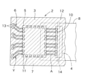
- FIG. 1 An example of such an optical communication module is schematically shown in FIG.
- This optical communication module has an optical / electric mixed board 2 integrally connected to a wiring board 1. More specifically, first, on the surface of the wiring board 1, a pair of two for differential signal transmission An electric wiring X in which a plurality of wirings are arranged is provided.
- the optical / electrical mixed substrate 2 includes an insulating layer 3 (indicated by diagonal grid lines in FIG. 12) having a wide portion and a narrow portion, and the back side of the wide portion of the insulating layer 3.
- An electric circuit unit 6 having an electric wiring Y, an optical element 4, and an optical element driving device (IC or the like) 5 is provided on the surface of the wiring board 1, that is, a surface overlapping the surface of the wiring board 1.
- the electric circuit portion 6 is covered with a coverlay at a portion requiring insulation.
- a metal reinforcing layer 7 is provided on the opposite surface (front surface in FIG. 12) of the insulating layer 3 provided with the electric circuit portion 6 to reinforce the electric circuit portion 6.
- An optical waveguide 8 is provided on the surface of the insulating layer 3 provided with the metal reinforcing layer 7 so as to partially overlap the metal reinforcing layer 7.
- a reflective surface for changing the path of light is formed in a portion of the optical waveguide 8 facing the optical element 4 with the insulating layer 3 interposed therebetween (not shown), and the light is reflected from the reflective surface. Light is optically coupled to the optical element 4.
- the metal reinforcing layer 7 is provided with a through hole 14 (see FIG. 13) so as not to obstruct the light path for the optical coupling.
- the electric circuit section 6 of the optical / electric mixed board 2 will be described in more detail with reference to FIG. 13, which is an enlarged view of this section. That is, in the electric circuit portion 6 provided on one side of the insulating layer 3, a pad 10 for mounting the optical element 4 (indicated by a one-point chain wire) and an optical element driving device 5 for driving the optical element 4 (indicated by a single point chain line) are provided. A pad 11 for mounting (indicated by a one-point chain wire such as an IC) is formed, and the electric wiring Y including the wiring portion A connecting the pads 10 and 11 is on the side opposite to the side on which the optical waveguide 8 extends. It extends to the edge.
- the electric wiring Y converts an optical signal into an electric signal and transmits it as a differential signal to the electric wiring X of the wiring board 1 (see FIG. 12).
- a terminal 13 serving as a connection point with the electric wiring X is provided. Then, except for the pads 10 and 11 and the terminal 13, the portion of the electric wiring Y or the like that requires insulation is covered with the coverlay 12 formed on this surface. In FIG. 13, the region where the coverlay 12 is formed is shown by a diagonal line rising to the right.
- Patent Document 2 an electric circuit that can perform a burn-in test of the optical element by switching with a switch is provided in the optical communication module, and it is possible to inspect the mounted optical element for initial defects before actual use. It has been proposed (Patent Document 2).
- an electric circuit for burn-in test of the optical element in the optical communication module because it is possible to inspect the presence or absence of the initial failure of the mounted optical element, but the inspection has nothing to do with the actual use. Since the electric circuit for the device is incorporated, there is a problem that the optical communication module is bulky and the manufacturing cost is high. Further, such a product incorporating an electric circuit for a burn-in test is expensive, and therefore, there is a problem that it is difficult to adopt it for consumer use.
- the present invention has been made in view of such circumstances, and although it has a simple configuration that can be adopted for consumer applications, it is possible to reliably perform a burn-in test on an optical element mounted on a substrate with high accuracy.
- an optical / electric mixed board that can obtain an optical communication module having excellent quality reliability at low cost, an optical communication module using the optical / electric mixed board, and an optical element inspection method in the optical communication module.
- the present invention provides the following [1] to [8].
- An electric circuit provided with an insulating layer and an electric wiring Y provided on the first surface side of the insulating layer and including a pad for mounting an optical element, a pad for an optical element driving device, and a wiring portion A connecting the pads.
- a part, a coverlay covering the electric circuit part, and an optical waveguide provided on the second surface side of the insulating layer are provided.
- the coverlay has an opening in a portion overlapping the wiring portion A, and the wiring portion A exposed from the opening is used as a burn-in test terminal for an optical element. ..
- the opening dimension J of the opening of the coverlay in the direction along the longitudinal direction of the wiring portion A is 0.
- the opto-electric mixed board according to the above [1] or [2] and a wiring board electrically connected to the opto-electric mixed board are provided. At least an optical element is mounted on the opto-electric mixed board, and the optical element is optically coupled to the optical waveguide of the opto-electric mixed substrate.
- An optical communication module in which a wiring portion A exposed from an opening provided in a coverlay of the optical / electric mixed substrate is used as a burn-in test terminal for the optical element.
- [5] In the step of obtaining the optical communication module according to the above [3] or [4], at least the optical element is mounted, and the optical element is optically coupled to the optical waveguide of the optical / electric mixed substrate, and the cover is covered.
- a current is passed through the optical element using the wiring portion A exposed from the opening of the ray as a terminal, and the current is converted into an optical signal by the optical element and output via the optical waveguide, and the output thereof is obtained.
- An optical element inspection method for inspecting the quality of the optical element by measuring the obtained optical signal [6] The optical element inspection according to the above [5], in which the optical element is inspected by passing a current having a current value 1.5 to 3 times the current value for driving the optical element in actual use. Method. [7] In the step of obtaining the optical communication module according to the above [3] or [4], at least the above optical element is mounted, and the above optical element is optically coupled to the optical waveguide of the above optical electric mixed substrate, and the above cover is provided. An optical element that inspects the quality of the optical element by applying a reverse bias voltage to the optical element and measuring the current generated in the optical element with the wiring portion A exposed from the opening of the ray as a terminal. Inspection method.
- the above optical element is mounted, and the above optical element is optically coupled to the optical waveguide of the above optical / electric mixed substrate.
- An optical signal is transmitted to the optical element via a waveguide, the optical signal is converted into an electric signal by the optical element, and the wiring portion A exposed from the opening of the coverlay is used as a terminal to obtain the electric signal.
- An optical element inspection method for inspecting the quality of the optical element by measuring the above.
- the present inventors have conducted a wiring portion connecting the optical element and the optical element drive device. If the light is exposed as an opening without being covered with a coverlay, the probe pin for the burn-in test can be electrically contacted with this exposed wiring part, so that the burn-in test can be easily performed. I found what I could do.
- the opto-electric mixed mounting substrate of the present invention although the structure is as simple as providing an opening in a part of the coverlay covering the electric circuit part, by conducting the probe pin in this part, the probe pin is surely provided. Moreover, a high-precision burn-in test can be performed.
- the opto-electric mixed mounting substrate is not obtained through a special process and can be easily obtained at low cost, so that it can be widely used for consumer applications. Further, since it is not necessary to bother to incorporate an electric circuit for the burn-in test, it is not necessary to provide an extra space on the optical / electric mixed board, and a compact structure can be maintained.
- the opening is not provided. Since the capacitance of the optical element is smaller than that of the above, there is an advantage that this optical / electric mixed substrate can be used in a higher frequency band. That is, in general, the larger the effective capacitance of the optical element mounted on the optical / electric mixed substrate, the lower the frequency band is on the lower frequency side than the high frequency band indicated by the optical element before mounting. On the other hand, if the opening is provided as described above, the electrostatic capacity generated between the wirings, which is added to the electrostatic capacity of the optical element itself, can be minimized. Therefore, after the optical element is mounted. However, the frequency band of the optical element before mounting is maintained, and a higher frequency signal can be transmitted.
- optical communication module of the present invention using the above-mentioned opto-electric mixed mounting substrate is inexpensive and compact, but can easily perform a burn-in test on the mounted optical element. It can be inspected and has excellent quality reliability.
- a burn-in test of the mounted optical element can be performed by a simple operation, and the presence or absence of an initial defect of the optical element can be confirmed from the optical characteristics and electrical characteristics. Can be done.
- This inspection can be easily performed before connecting the optical communication module to the target electrical / electronic equipment and laying it in a building or incorporating it inside the equipment, so that the light has excellent quality reliability.
- Communication modules can be provided.
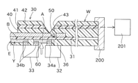
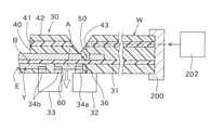
- FIG. 1 is an explanatory diagram schematically showing a main part of a photoelectric mixed mounting substrate according to an embodiment of the present invention by cutting along the extending direction of the optical waveguide.
- This optical / electric mixed board 30 is used for an optical communication module, and the basic configuration is the same as that of a general optical / electric mixed board. That is, an electric wiring Y in which a plurality of pairs of electric wirings for transmitting a differential signal are arranged on one surface (first surface) of one substantially band-shaped insulating layer 31 as a substrate, and an optical element.
- An electric circuit unit E provided with a pad 34a for mounting (photodiode, VCSEL, etc.) 32 and a pad 34b for mounting an optical element drive device (IC, etc.) 33 is provided (FIG. 2). reference). The portion of the electric circuit portion E that requires insulation protection is covered with the coverlay 36.
- the optical element 32 and the optical element drive device 33 may not be attached at the stage of the substrate, and are shown by a alternate long and short dash line.
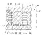
- the electric circuit section E of the optical / electric mixed board 30 will be described in more detail. That is, as shown in FIG. 2 when the optical circuit unit E is viewed from the side where the electric circuit unit E is formed, the optical element 32 shown by the diagonal line downward to the right is mounted on the electric circuit unit E. A pad 34a and a pad 34b for mounting the optical element drive device 33, which is also indicated by a diagonal line downward to the right, are provided. Further, at the end of the electric circuit unit E, a connection terminal 35 for connecting the optical / electric mixed board 30 to a wiring board having a signal transmission function to various electronic devices is provided.
- the electric wiring Y of the electric circuit unit E is a wiring portion A for connecting the pad 34a for the optical element 32 and the pad 34b for the optical element drive device 33, and a connection between the pad 34b and another wiring board. It is provided with a wiring portion B for connecting to the terminal 35.
- other wiring is also formed as needed, but the illustration is omitted.
- the electric circuit portion E is covered with a coverlay 36 at a portion requiring insulation protection.
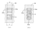
- the portion that requires insulation retention is usually the entire portion where the electrical wiring Y is formed, and the portion that requires energization such as the pads 34a and 34b for mounting the optical element 32 and the like and the connection terminal 35 and the like is Although excluded, in the present invention, in particular, the portion of the electrical wiring Y that overlaps with the wiring portion A connecting the pad 34a for mounting the optical element 32 and the pad 34b for the optical element drive device 33 is also covered with the coverlay 36. Is not formed, and this portion is a rectangular opening 60 that continuously straddles each wiring of the wiring portion A. This is a major feature of the present invention. In addition, in order to make it easy to understand, in FIG. 2, the region where the coverlay 36 is formed is shown by a diagonal line rising to the right.
- the metal reinforcing layer 37 for reinforcing the strength of the insulating layer 31 is provided on the other surface (second surface) of the insulating layer 31, that is, the surface opposite to the side on which the electric circuit portion E is provided. (Return to FIG. 1) is partially provided in the area requiring reinforcement. Similarly, the underclad layer 40, the core 41, and the overclad layer 42 are laminated in this order on the other surface of the insulating layer 31 in an arrangement that partially overlaps with the metal reinforcing layer 37, and these three layers are used.
- the optical waveguide W is formed.
- a part of the optical waveguide W is cut into an inclined surface, and the inclined surface serves as a light reflecting portion 43 for changing the traveling direction of an optical signal transmitted via the core 41 by 90 °. ing.
- a through hole 50 is formed in the metal reinforcing layer 37 so as not to obstruct the path of light optically coupled to the optical element 32 via the light reflecting portion 43.
- a metal plate 100 to be a metal reinforcing layer 37 is prepared, and a photosensitive insulating resin such as polyimide is coated on the surface of the metal plate 100 to form an insulating layer 31.
- the insulating resin layer 101 is formed.
- Examples of the material of the metal plate 100 include stainless steel, copper, silver, aluminum, nickel, chromium, titanium, platinum, gold and the like, but stainless steel is preferable from the viewpoint of strength, flexibility and the like. Further, it is preferable to set the thickness of the metal reinforcing layer 37 in the range of, for example, 10 to 70 ⁇ m (more preferably 10 to 30 ⁇ m).
- the insulating resin layer 101 is subjected to a photolithography method (exposure, prebaking, development, curing) to form an insulating layer 31 having a predetermined pattern shape.
- the thickness of the insulating layer 31 is preferably set within the range of, for example, 3 to 50 ⁇ m (more preferably 3 to 25 ⁇ m) (this step is not shown).
- a conductive layer made of a conductive material such as copper is formed on the insulating layer 31 by sputtering or electroless plating, and then through necessary treatments such as dry film resist laminating, exposure, and development.
- a conductive pattern is formed such as an electric wiring Y including wiring portions A and B, various pads 34a and 34b, and a connection terminal 35.
- a photosensitive insulating resin such as polyimide is applied on the conductive pattern, and a coverlay 36 is formed in a portion requiring insulation protection in the same manner as the formation of the insulating layer 31. do.
- the coverlay 36 is provided with an opening 60 (see FIG. 2) for exposing the wiring portion A as well as an opening for exposing the pad 34a and the like.
- a metal material having excellent conductivity and malleability such as chrome, aluminum, gold, and tantalum is preferably used in addition to copper. Further, alloys using at least one of these metals are also preferably used.
- the thickness of the conductive pattern of the electric wiring Y or the like is preferably set in the range of 3 to 30 ⁇ m (more preferably 3 to 18 ⁇ m). Further, the thickness of the coverlay 36 formed on the coverlay 36 should be set in the range of, for example, 1 to 50 ⁇ m (more preferably 1 to 25 ⁇ m) in consideration of insulation protection such as electric wiring Y and further reinforcement. Is preferable.
- the electric circuit portion E can be obtained by forming an electrolytic plating layer of nickel, gold or the like on the portions of the various pads 34a and 34b and the connection terminals 35 exposed from the coverlay 36 (FIG. FIG.). See 4).
- etching treatment dry film resist laminating, exposure, development, etching, drying
- Removal of film resist, etc. is performed to remove unnecessary parts to obtain a predetermined pattern shape.
- necessary openings and notches such as a through hole 50 for optical coupling with the optical element 32 (see FIG. 1) are provided.
- the insulating layer 31 provided with the electric circuit portion E and the metal reinforcing layer 37 is turned upside down, and the metal reinforcing layer 37 is turned upward.
- the underclad layer 40, the core 41, and the overclad layer 42 are patterned on the surface of the insulating layer 31 on the side where the metal reinforcing layer 37 is formed by a known method, and each layer is patterned in a predetermined pattern as needed.
- the optical waveguide W can be obtained by laminating and forming in this state.
- the predetermined portion of the optical waveguide W is formed by dicing, laser processing, cutting, or the like to form the core 41.
- the light reflecting portion 43 is formed on an inclined surface inclined by 45 ° with respect to the longitudinal direction. In this way, the photoelectric mixed mounting substrate 30 shown in FIG. 1 can be obtained.
- the tip side (not shown) on the side opposite to the side facing the electric circuit portion E is configured to have an optical connector for connecting to another optical wiring member. There is.
- the coverlay 36 covering the surface of the electric circuit portion E overlaps with the wiring portion A connecting the pad 34a for mounting the optical element 32 and the pad 34b for the optical element drive device 33. Is not formed and is an opening 60, so that the wiring portion A is exposed from the opening 60. Therefore, according to the opto-electric mixed mounting substrate 30, although the structure is as simple as providing an opening 60 in a part of the coverlay 36 covering the electric circuit part E, the probe pin is made conductive in this part. The burn-in test can be performed reliably and with high accuracy.
- the opto-electric mixed substrate 30 does not need to be obtained via a special process and can be easily obtained at low cost, so that it can be widely used for consumer applications. Further, since it is not necessary to bother to incorporate an electric circuit for the burn-in test, it is not necessary to provide an extra space in the optical / electric mixed board 30.
- the opening 60 is not provided. Since the capacitance of the optical element 32 is smaller than in the case, there is an advantage that the optical / electric mixed substrate 30 can be used in a higher frequency band.
- the optical / electric mixed board 30 thus obtained is used alone or is connected to a wiring board 20 used in various electric / electronic devices, for example, as shown in FIG. It can be used as an optical communication module board. Then, the necessary devices are mounted on this board to form an optical communication module.
- the wiring board 20 for example, an electric circuit including an electric wiring X and a connection terminal 22 is provided on the surface of the board (rigid board or flexible board) 21, and the portion of the surface that requires insulation is the insulating layer 23. It has a structure covered with.
- connection terminals 35 and 22 are opposed to each other so as to be vertically overlapped with each other, and the facing connection terminals 35 and 22 are electrically connected by a solder bump or the like. It is done by connecting to the target.
- the above optical communication module is inexpensive and compact, it can easily perform a burn-in test on the mounted optical element, so that it can be inspected for the presence or absence of initial defects and has excellent quality reliability. It becomes a thing.
- the burn-in test can be easily performed at a stage prior to the laying or assembly. It is very useful because it can be done in.
- the method for inspecting an optical element in the optical communication module can be performed as follows, for example. That is, first, as shown in FIG. 7, an optical element (light emitting element: VCSEL) 32 is mounted on the optical / electric mixed mounting substrate 30 of the optical communication module. Then, the optical communication module is arranged in a constant temperature bath set to a predetermined temperature, and the wiring portion A exposed from the opening 60 provided in the coverlay 36 (hatched portion) in the vicinity of the optical element 32. A burn-in test can be easily performed by connecting a probe pin to the wire and passing a larger current than in actual use. Then, the optical communication module taken out from the constant temperature bath is inspected for any defects in the optical element 32.
- an optical element (light emitting element: VCSEL) 32 is mounted on the optical / electric mixed mounting substrate 30 of the optical communication module. Then, the optical communication module is arranged in a constant temperature bath set to a predetermined temperature, and the wiring portion A exposed from the opening 60 provided in the coverlay 36 (hatched portion) in
- FIG. 8 schematically shows a vertical cross section of the optical / electric mixed mounting substrate 30. That is, first, in order to expose the optical element 32 to harsh conditions, the optical communication module is placed in a constant temperature bath set to a predetermined high temperature (for example, 60 to 120 ° C.), and the electric circuit of the optical / electric mixed substrate 30 is provided. A probe pin is connected to the wiring portion A exposed from the opening 60 of the coverlay 36 on the surface on the side where the portion E is formed, as shown by a white arrow. Then, a large current is passed from the wiring portion A to the optical element 32. Thereby, it is tested whether or not the light emission of the optical element 32 is performed without any trouble even under severe conditions. At this time, as shown by the broken line, the optical signal propagates in the optical waveguide W.
- a predetermined high temperature for example, 60 to 120 ° C.
- the optical communication module is taken out from the constant temperature bath, and the power meter 201 (for example, an optical power meter manufactured by ADC: 8250A and optical) is connected to the other end of the optical waveguide W of the optical communication module via an optical connector 200.
- a sensor: 82321B was connected, and a current was passed through the wiring portion A exposed from the opening 60 of the coverlay 36 of the optical / electric mixed substrate 30 to cause the optical element 32 to emit light, which was propagated from the optical waveguide W. Measure the optical signal. The presence or absence of initial defects in the optical element 32 can be inspected depending on whether or not this optical signal indicates a measured value within an appropriate standard.
- the current value to be passed through the wiring portion A for burn-in it is preferable to set the current value to be passed through the wiring portion A for burn-in to 1.5 to 3 times the current value to be passed through the optical element 32 during actual use. That is, if the current value is smaller than the above range, the initial defect of the optical element 32 may not be correctly inspected in a short time, and conversely, if it is larger than the above range, the optical element 32 originally has. This is because the allowable current value may be exceeded and even the normal optical element 32 may be destroyed.
- the above example is an example in which the burn-in test is performed at the stage where only the optical element 32 is mounted.
- the above burn-in test is performed on both the optical element 32 and the optical element drive device 33.
- the space between the two may be used.
- the burn-in test method is the same as the example shown in FIG. 8, and the description thereof will be omitted.
- the optical communication module is placed at a high temperature by using a burn-in device, a large current is applied to the optical element 32 by using the wiring portion A, and then this is taken out to improve the quality of the optical element 32.
- the burn-in test does not necessarily have to be performed in such two stages. For example, an optical signal propagated through the tip of the optical waveguide W is converted into an electric signal by a light receiving element (for example, PD) connected to the optical signal while passing a large current from the wiring portion A, and the measured value thereof. Therefore, the presence or absence of initial defects of the optical element 32 may be inspected.
- a light receiving element for example, PD
- a current is passed through the optical element 32 to perform a burn-in test.
- the tip of the optical waveguide W is connected to the tip of the optical waveguide W via an optical connector 200.
- a light source 202 propagate it as an optical signal in the optical waveguide W as shown by a broken line, change it into an electric signal in the optical element (light receiving element) 32, and inspect its quality. That is, the initial stage of the optical element 32 is measured by measuring the electric signal converted in the optical element 32 with an electrometer (for example, an electrometer 5350 manufactured by ADC) connected to the wiring portion A exposed from the opening 60. It is possible to inspect for defects.
- the optical signal is not propagated to the optical element 32 but is exposed from the opening 60 of the coverlay 36.
- a method of applying a reverse bias voltage to the optical element 32 with the wiring portion A as a terminal and measuring the current (dark current) generated in the optical element 32 can be mentioned.
- the quality of the optical element 32 can be inspected assuming that there is no problem in the quality of the optical element 32 as long as this current does not exceed a predetermined magnitude.
- the voltage is usually applied by arranging the optical communication module in a constant temperature bath (for example, set to 60 to 120 ° C.) for a predetermined time.
- the opening 60 of the coverlay 36 has the longitudinal dimension of the wiring portion A [indicated by H in FIG. 2] as 1, and the opening 60 of the opening 60 in the longitudinal direction of the wiring portion A. It is preferable to set the opening size [indicated by J in FIG. 2] to be 0.5 to 1.2. That is, if the opening dimension J of the opening 60 along the longitudinal direction of the wiring portion A is too smaller than the above range, it becomes difficult to connect to the tip of the probe pin for the burn-in test, which is not preferable. Considering that the larger the opening 60 is, the smaller the capacitance of the mounted optical element 32 tends to be, the ratio of J to H is particularly 0 in the above range. It is more preferable to set it to 0.8 to 1.
- the opening 60 of the coverlay 36 does not have to be provided only in the portion overlapping the wiring portion A.
- the opening may include the space between the pads 34a and the space between the pads 34b.
- the opening 60 does not have to be a single opening, and as shown in FIG. 11B, for example, a plurality of individual openings 60a are individually opened for each channel for a plurality of channels. (4 in this example) may be used. According to this configuration, since the portion of the coverlay 36 remains as a partition between each channel, the opening edge of each opening 60a is difficult to peel off, although it is inferior to the above example in terms of the effect of removing electrostatic capacitance. Has advantages. In addition, since the individual openings are provided for each channel, the electrical insulation effect between the channels is also improved.
- the type of the signal flowing through the wiring portion A and the wiring portion B is not particularly limited, and an appropriate one is selected according to the type of the optical element 32 to be connected, various devices, and the like. ..
- Examples of the signal type include a single-ended signal, a differential signal, a coplanar signal, and the like.
- an optical communication module substrate having the configuration shown in FIG. 6 was manufactured.
- the materials and thicknesses of the main configurations are as follows.
- Insulation layer 31 polyimide, thickness 15 ⁇ m Electrical wiring Y of the electric circuit part (including wiring parts A and B): Copper, thickness 10 ⁇ m (each pad, with terminal gold plating) Coverlay 36: Polyimide, thickness 5 ⁇ m (thickness from the surface of the insulating layer 31) Metal reinforcing layer 37: Stainless steel, thickness 20 ⁇ m Underclad layer 40: Photocurable epoxy resin composition, thickness 30 ⁇ m Core 41: Photocurable epoxy resin composition, thickness 40 ⁇ m Overclad layer 42: Photocurable epoxy resin composition, thickness 70 ⁇ m (thickness from the surface of underclad layer 40)
- Substrate 21 Glass epoxy resin (FR4, 4-layer through plate), total thickness 1.6 mm Electrical wiring X: Copper, thickness 35 ⁇ m (each pad, with terminal gold plating)
- Optical element 32 VCSEL (Product number: APA4401040001, manufactured by II-VI LASER ENTERPRISE)
- Optical element drive device 33 IC (Product number: SL82817, manufactured by SILICON LINE)
- Example 1 Of the 100 inspection targets, 6 are optical communication modules equipped with the VCSEL subjected to the ESD test, and the remaining 94 modules are mounted with a normal VCSEL not subjected to the ESD test. These 100 optical communication modules were arranged in a constant temperature bath at 85 ° C., and 10 mA of direct current was continuously energized to the VCSEL from the wiring portion A exposed from the opening 60 of the optical / electric mixed substrate 30 for 100 hours.
- a DC stabilized power supply: PMX35-1A manufactured by Kikusui Denshi Co., Ltd. was connected to the wiring portion A exposed from the opening 60 of the optical-electric mixed board 30.
- the optical signal converted in the optical element 32 while flowing 6 mA was measured by a power meter coupled to the optical waveguide W. If the optical output is out of the standard, it is judged as defective.
- the optical output of the 6 modules equipped with the VCSEL that was subjected to the ESD test was out of specification for 100 inspection targets.
- the optical output was within the standard.
- Example 2 In the optical communication module, as shown in FIG. 9, the VCSEL and the optical element drive device 33 were mounted on the optical / electric mixed mounting substrate 30, and then the inspection was performed in the same manner as in the first embodiment. Similar to the first embodiment, six of the 100 inspection targets are modules on which the VCSEL subjected to the ESD test is mounted.
- the optical output of the 6 modules equipped with the VCSEL that was subjected to the ESD test was out of specification for 100 inspection targets.
- the optical output was within the standard.
- the optical communication module using the same, and the optical element inspection method of the optical communication module it is possible to easily inspect the presence or absence of initial defects of the optical element mounted on the optical communication module. Therefore, it can be widely used for providing an optical communication module having excellent quality and reliability.
Landscapes
- Physics & Mathematics (AREA)
- General Physics & Mathematics (AREA)
- Optics & Photonics (AREA)
- Engineering & Computer Science (AREA)
- Microelectronics & Electronic Packaging (AREA)
- Condensed Matter Physics & Semiconductors (AREA)
- Electromagnetism (AREA)
- Optical Integrated Circuits (AREA)
- Semiconductor Lasers (AREA)
Abstract
光通信モジュール用の光電気混載基板(30)であって、絶縁層(31)の第1の面側に、光素子(32)実装用のパッド(34a)と、光素子駆動デバイス(33)用のパッド(34b)と、それらを繋ぐ配線部分Aを含む電気配線Yとを有する電気回路部Eが設けられ、上記絶縁層(31)の第2の面側に、光導波路Wを設けられている。そして、上記電気回路部Eを被覆するカバーレイ(36)の、上記配線部分Aと重なる部分が除去されて開口部(60)が形成されており、上記開口部(60)から露出する上記配線部分Aが、光素子(32)に対するバーンインテスト用端子として用いられるようになっている。この光電気混載基板(30)によれば、簡単な構成でありながら、基板(30)に実装された光素子(32)に対するバーンインテストを高い精度で確実に行うことができ、品質信頼性に優れた光通信モジュールを低コストで提供することができる。
Description
本発明は、光電気混載基板およびそれを用いた光通信モジュール、並びにその光通信モジュールの光素子検査方法に関し、とりわけ上記光通信モジュールに実装される光素子の初期不良の有無を簡単に検査することができ、品質信頼性に優れた光通信モジュールを提供することのできる技術に関するものである。
最近の電子機器では、伝送情報量の増加に伴い、電気配線に加えて光配線が採用されており、電気配線と光配線をコンパクトに配置した光電気混載基板が賞用されている。また、上記光電気混載基板を、各種電子機器への信号伝送機能を備えた配線基板等にさらに接続して高速信号伝送を行う光通信モジュール等への使用も広がっている。
このような光通信モジュールの一例を、図12に模式的に示す。この光通信モジュールは、配線基板1に光電気混載基板2を一体的に接続したもので、より詳しく説明すると、まず、上記配線基板1の表面には、差動信号伝送用の2本一対の配線を複数並べた電気配線Xが設けられている。
また、上記光電気混載基板2は、幅の広い部分と狭い部分とを備えた絶縁層3(図12において斜格子状の線で示す)を備え、上記絶縁層3の幅の広い部分の裏側の面、すなわち上記配線基板1の表面に重なる面に、電気配線Yや光素子4、光素子駆動デバイス(IC等)5を有する電気回路部6が設けられている。そして、上記電気回路部6は、絶縁の必要な部分がカバーレイによって被覆されている。
一方、上記電気回路部6が設けられた絶縁層3の反対側の面(図12において表側の面)には、電気回路部6を補強するために金属補強層7が設けられており、この金属補強層7が設けられた絶縁層3の面に、上記金属補強層7と一部が重なる形で、光導波路8が設けられている。そして、上記光導波路8の、絶縁層3を挟んで光素子4と対峙する部分に、光の行路を変更するための反射面が形成されており(図示せず)、その反射面から反射する光が光素子4と光結合されるようになっている。なお、上記金属補強層7には、上記光結合のための光の行路を妨げないように、貫通孔14(図13を参照)が設けられている。
上記光電気混載基板2の電気回路部6を、この部分を拡大して模式的に示す図13を用いて、より詳しく説明する。すなわち、絶縁層3の片面に設けられる電気回路部6には、光素子4(一点鎖線で示す)を実装するためのパッド10と、この光素子4を駆動するための光素子駆動デバイス5(IC等、一点鎖線で示す)を実装するためのパッド11とが形成されており、上記パッド10、11を接続する配線部分Aを含む電気配線Yが、光導波路8が延びる側と反対側の端縁まで延びている。
上記電気配線Yは、光信号を電気信号に変換し、差動信号として、配線基板1(図12参照)の電気配線Xに伝送するようになっており、電気配線Yの先端には、上記電気配線Xとの接続点となる端子13が設けられている。そして、上記パッド10、11や端子13等を除き、電気配線Y等の、絶縁が必要な部分が、この面に形成されたカバーレイ12によって被覆されている。なお、図13において、カバーレイ12が形成された領域を右上がりの斜線で示す。
このような光通信モジュールを用いて、画像情報や音声情報を含む、膨大な情報をより高速で精度よく伝送するニーズが高まっており、光配線のさらなる緻密化と、電気信号、光信号のより高周波数化が強く求められている。また、上記光通信モジュールを、電気・電子機器に組み込んでしまうと、使用時に不具合が生じても、即座に修理したり部材の交換を行ったりすることが困難な場合が多いため、例えば、上記光通信モジュールに実装する光素子を、実装前に単体でバーンインテストにかけて、初期不良が発生するおそれのあるものを予め排除することが提案されている(特許文献1を参照)。
さらに、光通信モジュール内に、スイッチで切り換えることによって光素子のバーンインテストを行うことのできる電気回路を設け、実際の使用に先立って、実装された光素子の初期不良の有無を検査することが提案されている(特許文献2)。
しかしながら、光素子を単体でバーンインテストする方法では、実際に基板に実装し、光導波路と光結合した状態で光素子に不具合が生じる「初期不良」を見つけることができないため、光通信モジュールとしての品質信頼性を充分に担保するものとはいえない。
また、光通信モジュール内に、光素子のバーンインテスト用の電気回路を設けたものは、実装された光素子の初期不良の有無を検査できる点で好ましいが、実際の使用とは関係のない検査用の電気回路を組み込んでいるため、光通信モジュールが嵩張り、また製造コストも高くなるという問題がある。そして、このような、バーンインテスト用の電気回路を組み込んだものは高価になるため、民生用途において採用しにくいという問題もある。
本発明はこのような事情に鑑みなされたもので、民生用途にも採用しうる、簡単な構成でありながら、基板に実装された光素子に対するバーンインテストを高い精度で確実に行うことができ、品質信頼性に優れた光通信モジュールを低コストで得ることのできる光電気混載基板と、その光電気混載基板を用いた光通信モジュールと、その光通信モジュールにおける光素子検査方法とを提供する。
すなわち、本発明は、以下の[1]~[8]を提供する。
[1]光通信モジュールに用いられる光電気混載基板であって、
絶縁層と、上記絶縁層の第1の面側に設けられ、光素子実装用のパッドと光素子駆動デバイス用のパッドとそれらのパッドを繋ぐ配線部分Aを含む電気配線Yとを有する電気回路部と、上記電気回路部を被覆するカバーレイと、上記絶縁層の第2の面側に設けられた光導波路とを備え、
上記カバーレイが、上記配線部分Aと重なる部分において開口部を有し、上記開口部から露出する上記配線部分Aが、光素子に対するバーンインテスト用端子として用いられるようになっている光電気混載基板。
[2]上記配線部分Aの、両側のパッドを含む長手方向の寸法Hを1とすると、上記カバーレイの開口部の、上記配線部分Aの長手方向に沿う方向の開口寸法Jが、0.5~1.2に設定されている上記[1]記載の光電気混載基板。
[3]上記[1]または[2]記載の光電気混載基板と、上記光電気混載基板に電気的に接続される配線基板とを備え、
上記光電気混載基板には、少なくとも光素子が実装され、上記光素子が上記光電気混載基板の光導波路と光結合しており、
上記光電気混載基板のカバーレイに設けられた開口部から露出する配線部分Aが、上記光素子に対するバーンインテスト用端子として用いられるようになっている光通信モジュール。
[4]上記光通信モジュールが、民生用途である上記[3]記載の光通信モジュール。
[5]上記[3]または[4]記載の光通信モジュールを得る工程において、少なくとも上記光素子を実装し、上記光素子を上記光電気混載基板の光導波路と光結合した状態で、上記カバーレイの開口部から露出する上記配線部分Aを端子として、上記光素子に対して電流を流し、その電流を上記光素子で光信号に変換して上記光導波路を経由して出力させ、その出力された光信号を計測することにより、上記光素子の品質を検査する光素子検査方法。
[6]上記光素子に対し、実際に使用する際の光素子駆動用の電流値の1.5~3倍の電流値となる電流を流して検査を行う上記[5]記載の光素子検査方法。
[7]上記[3]または[4]記載の光通信モジュールを得る工程において、少なくとも上記光素子を実装し、上記光素子を上記光電気混載基板の光導波路と光結合した状態で、上記カバーレイの開口部から露出する上記配線部分Aを端子として、上記光素子に対して逆バイアス電圧を印加し、上記光素子に生じる電流を計測することにより、上記光素子の品質を検査する光素子検査方法。
[8]上記[3]または[4]記載の光通信モジュールを得る工程において、少なくとも上記光素子を実装し、上記光素子を上記光電気混載基板の光導波路と光結合した状態で、上記光導波路を経由して光信号を上記光素子に伝送し、その光信号を上記光素子で電気信号に変換して、上記カバーレイの開口部から露出する上記配線部分Aを端子として、上記電気信号を計測することにより、上記光素子の品質を検査する光素子検査方法。
[1]光通信モジュールに用いられる光電気混載基板であって、
絶縁層と、上記絶縁層の第1の面側に設けられ、光素子実装用のパッドと光素子駆動デバイス用のパッドとそれらのパッドを繋ぐ配線部分Aを含む電気配線Yとを有する電気回路部と、上記電気回路部を被覆するカバーレイと、上記絶縁層の第2の面側に設けられた光導波路とを備え、
上記カバーレイが、上記配線部分Aと重なる部分において開口部を有し、上記開口部から露出する上記配線部分Aが、光素子に対するバーンインテスト用端子として用いられるようになっている光電気混載基板。
[2]上記配線部分Aの、両側のパッドを含む長手方向の寸法Hを1とすると、上記カバーレイの開口部の、上記配線部分Aの長手方向に沿う方向の開口寸法Jが、0.5~1.2に設定されている上記[1]記載の光電気混載基板。
[3]上記[1]または[2]記載の光電気混載基板と、上記光電気混載基板に電気的に接続される配線基板とを備え、
上記光電気混載基板には、少なくとも光素子が実装され、上記光素子が上記光電気混載基板の光導波路と光結合しており、
上記光電気混載基板のカバーレイに設けられた開口部から露出する配線部分Aが、上記光素子に対するバーンインテスト用端子として用いられるようになっている光通信モジュール。
[4]上記光通信モジュールが、民生用途である上記[3]記載の光通信モジュール。
[5]上記[3]または[4]記載の光通信モジュールを得る工程において、少なくとも上記光素子を実装し、上記光素子を上記光電気混載基板の光導波路と光結合した状態で、上記カバーレイの開口部から露出する上記配線部分Aを端子として、上記光素子に対して電流を流し、その電流を上記光素子で光信号に変換して上記光導波路を経由して出力させ、その出力された光信号を計測することにより、上記光素子の品質を検査する光素子検査方法。
[6]上記光素子に対し、実際に使用する際の光素子駆動用の電流値の1.5~3倍の電流値となる電流を流して検査を行う上記[5]記載の光素子検査方法。
[7]上記[3]または[4]記載の光通信モジュールを得る工程において、少なくとも上記光素子を実装し、上記光素子を上記光電気混載基板の光導波路と光結合した状態で、上記カバーレイの開口部から露出する上記配線部分Aを端子として、上記光素子に対して逆バイアス電圧を印加し、上記光素子に生じる電流を計測することにより、上記光素子の品質を検査する光素子検査方法。
[8]上記[3]または[4]記載の光通信モジュールを得る工程において、少なくとも上記光素子を実装し、上記光素子を上記光電気混載基板の光導波路と光結合した状態で、上記光導波路を経由して光信号を上記光素子に伝送し、その光信号を上記光素子で電気信号に変換して、上記カバーレイの開口部から露出する上記配線部分Aを端子として、上記電気信号を計測することにより、上記光素子の品質を検査する光素子検査方法。
本発明者らは、光通信モジュールにおいて、実装した光素子に対して簡単で確実にバーンインテストを行うことのできる構造について鋭意検討を重ねた結果、光素子と光素子駆動デバイスとを繋ぐ配線部分を、カバーレイで被覆せずに開口部としてそこから露出させておけば、この露出した配線部分に、バーンインテスト用のプローブピンを導通コンタクトすることができるため、簡単にバーンインテストを行うことができることを見いだした。
本発明の光電気混載基板によれば、電気回路部を被覆するカバーレイの一部に開口部を設けるだけの単純な構成でありながら、この部分にプローブピンを導通させることにより、確実に、しかも高精度のバーンインテストを行うことができる。そして、上記光電気混載基板は、特殊な工程を経由して得られるものではなく、低コストで簡単に得ることができるため、民生用途にも広く用いることができる。そして、バーンインテスト用としてわざわざそのための電気回路を組み込む必要がないため、光電気混載基板に余分なスペースを設ける必要がなく、コンパクトな構造を維持することができる。
しかも、上記のように、光電気混載基板において、電気回路部を被覆するカバーレイに開口部を設けて光素子と光素子駆動デバイスとを繋ぐ配線部分を露出させると、開口部を設けない場合に比べて、光素子の静電容量が小さくなるため、この光電気混載基板をより高周波数帯域で使用することができる、という利点を有する。すなわち、一般に、光電気混載基板に実装された光素子の実効的な静電容量が大きくなればなるほど、周波数帯域が、その光素子が実装前に示していた高周波数帯域よりも低周波数側に遷移するのに対し、上記のように開口部を設けると、光素子自体がもつ静電容量に付加される、配線間で発生する静電容量を極力小さくすることができるため、光素子実装後も、実装前の光素子の周波数帯域が維持されて、より高周波数の信号を伝送することができる。
また、上記光電気混載基板を用いた本発明の光通信モジュールは、低価格でコンパクトでありながら、実装した光素子に対して簡単にバーンインテストを行うことができるため、その初期不良の有無を検査することができ、品質信頼性に優れたものとなる。
そして、本発明の光素子検査方法によれば、簡単な操作で、実装された光素子のバーンインテストを行うことができ、その光特性、電気特性から光素子の初期不良の有無を確認することができる。この検査は、光通信モジュールを、目的とする電気・電子機器と接続して建物に敷設したり装置の内部に組み込んだりする前に、簡単に行うことができるため、品質信頼性に優れた光通信モジュールを提供することができる。
つぎに、本発明の実施の形態を、図面にもとづいて詳しく説明する。ただし、本発明は以下の形態に限定されるものではない。
図1は、本発明の一実施の形態である光電気混載基板の要部を、光導波路の延びる方向に沿って切断して模式的に示す説明図である。
この光電気混載基板30は、光通信モジュールに用いられるもので、基本的な構成は、一般的な光電気混載基板と同じである。すなわち、一枚の略帯状の絶縁層31を基板として、その片面(第1の面)に、差動信号を伝送するための2本一対の電気配線を複数並べた電気配線Yと、光素子(フォトダイオード、VCSEL等)32を実装するためのパッド34aや、光素子駆動デバイス(IC等)33を実装するためのパッド34b等を備えた電気回路部Eが設けられている(図2を参照)。そして、上記電気回路部Eの、絶縁保護の必要な部分がカバーレイ36で被覆されている。なお、光素子32、光素子駆動デバイス33は、基板の段階では取り付けないことがあり、一点鎖線で示している。
上記光電気混載基板30の電気回路部Eについて、より詳しく説明する。すなわち、上記電気回路部Eには、上記光電気混載基板30をこの電気回路部Eが形成された側から見た図2に示すとおり、右下がりの斜線で示す光素子32を実装するためのパッド34aと、同じく右下がりの斜線で示す光素子駆動デバイス33を実装するためのパッド34bとが設けられている。また、上記電気回路部Eの端部には、この光電気混載基板30を、各種電子機器への信号伝送機能を備えた配線基板に接続するための接続用端子35が設けられている。
そして、上記電気回路部Eの電気配線Yは、光素子32用のパッド34aと光素子駆動デバイス33用のパッド34bとを接続する配線部分Aと、上記パッド34bと他の配線基板用の接続用端子35とを接続する配線部分Bとを備えている。もちろん、必要に応じて他の配線も形成されるが、その図示を省略している。
上記電気回路部Eは、すでに述べたとおり、絶縁保護の必要な部分がカバーレイ36で被覆されている。絶縁保持の必要な部分とは、通常、電気配線Yが形成されている部分全部であり、光素子32等の実装するためのパッド34a、34bや接続用端子35等、通電が必要な部分は除かれるが、本発明では、特に、上記電気配線Yのうち、上記光素子32実装用のパッド34aと光素子駆動デバイス33用のパッド34bとを繋ぐ配線部分Aと重なる部分も、カバーレイ36が形成されておらず、この部分が、配線部分Aの各配線を連続的にまたぐ長方形状の開口部60になっている。これが、本発明の大きな特徴である。なお、わかりやすく見せるために、図2において、カバーレイ36が形成されている領域を、右上がりの斜線で示す。
一方、上記絶縁層31の他面(第2の面)、すなわち電気回路部Eが設けられている側と反対側の面には、上記絶縁層31の強度を補強するための金属補強層37(図1に戻る)が、補強を必要とする領域に、部分的に設けられている。また、同じく上記絶縁層31の他面に、上記金属補強層37と部分的に重なる配置で、アンダークラッド層40、コア41、オーバークラッド層42がこの順で積層されており、これら3層によって光導波路Wが形成されている。なお、上記光導波路Wの一部が傾斜面にカットされており、その傾斜面が、コア41を経由して伝送される光信号の進行方向を90°変更するための光反射部43になっている。そして、上記金属補強層37には、この光反射部43を経由して光素子32と光結合する光の行路を妨げないように、貫通孔50が形成されている。
<光電気混載基板の形成工程>
つぎに、上記光電気混載基板30を得る工程の一例を、具体的な材料を例示しつつ簡単に説明する。
(1)電気回路部Eの形成
まず、図3に示すように、金属補強層37となる金属板100を用意し、その表面に、ポリイミド等の感光性絶縁樹脂を塗布して、絶縁層31となる絶縁樹脂層101を形成する。
つぎに、上記光電気混載基板30を得る工程の一例を、具体的な材料を例示しつつ簡単に説明する。
(1)電気回路部Eの形成
まず、図3に示すように、金属補強層37となる金属板100を用意し、その表面に、ポリイミド等の感光性絶縁樹脂を塗布して、絶縁層31となる絶縁樹脂層101を形成する。
上記金属板100の材料としては、ステンレス、銅、銀、アルミニウム、ニッケル、クロム、チタン、白金、金等があげられるが、強度性、屈曲性等の観点から、ステンレスが好ましい。また、上記金属補強層37の厚みは、例えば、10~70μm(より好ましくは10~30μm)の範囲内に設定することが好適である。
そして、上記絶縁樹脂層101に対し、フォトリソグラフィ法(露光、プリベイク、現像、キュア)を施して、所定のパターン形状を有する絶縁層31を形成する。上記絶縁層31の厚みは、例えば、3~50μm(より好ましくは3~25μm)の範囲内に設定することが好適である(この工程は図示せず)。
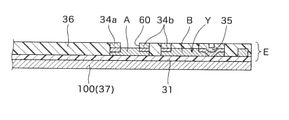
つぎに、上記絶縁層31の上に、スパッタもしくは無電解メッキ等により銅等の導電材料からなる導電層を形成した後、ドライフィルムレジストラミネート、露光、現像等の必要な処理を経由して、配線部分A、Bを含む電気配線Yや各種パッド34a、34b、接続用端子35等の導電パターンを形成する。そして、図4に示すように、この導電パターンの上に、ポリイミド等の感光性絶縁樹脂を塗布し、前記絶縁層31の形成と同様にして、絶縁保護が必要な部分にカバーレイ36を形成する。このとき、カバーレイ36には、パッド34a等を露出させるための開口とともに、配線部分Aを露出させるための開口部60(図2参照)が設けられる。
なお、上記導電パターンを形成する導電材料としては、銅の他、クロム、アルミニウム、金、タンタル等、導電性および展性に優れた金属材料が好適に用いられる。また、これらの金属の少なくとも一種を用いた合金も好適に用いられる。そして、上記電気配線Y等の導電パターンの厚みは、3~30μm(より好ましくは3~18μm)の範囲に設定することが好適である。また、その上に形成されるカバーレイ36の厚みは、電気配線Y等の絶縁保護、さらには補強を考慮して、例えば、1~50μm(より好ましくは1~25μm)の範囲に設定することが好適である。
そして、上記カバーレイ36から露出する、各種パッド34a、34bや接続用端子35となる部分に、ニッケル、金等の電解めっき層を形成することにより、電気回路部Eを得ることができる(図4を参照)。
(2)金属補強層37のパターン形成
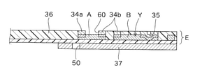
つぎに、上記絶縁層31を挟んで電気回路部Eとは反対側の金属補強層37に、エッチング処理(ドライフィルムレジストラミネート、露光、現像、エッチング、ドライフィルムレジスト剥離等)を施して、不要な部分を除去して、所定のパターン形状にする。これにより、図5に示すように、光素子32(図1を参照)との光結合用の貫通孔50等の必要な開口や切欠きが設けられる。
つぎに、上記絶縁層31を挟んで電気回路部Eとは反対側の金属補強層37に、エッチング処理(ドライフィルムレジストラミネート、露光、現像、エッチング、ドライフィルムレジスト剥離等)を施して、不要な部分を除去して、所定のパターン形状にする。これにより、図5に示すように、光素子32(図1を参照)との光結合用の貫通孔50等の必要な開口や切欠きが設けられる。
(3)光導波路Wの形成
つぎに、上記電気回路部Eと金属補強層37を備えた絶縁層31を上下逆にして、金属補強層37を上に向ける。そして、上記絶縁層31の、金属補強層37が形成された側の面に、公知の方法によってアンダークラッド層40とコア41とオーバークラッド層42とを、必要に応じて各層を所定パターンにパターニングした状態で積層形成することにより、光導波路Wを得ることができる。
つぎに、上記電気回路部Eと金属補強層37を備えた絶縁層31を上下逆にして、金属補強層37を上に向ける。そして、上記絶縁層31の、金属補強層37が形成された側の面に、公知の方法によってアンダークラッド層40とコア41とオーバークラッド層42とを、必要に応じて各層を所定パターンにパターニングした状態で積層形成することにより、光導波路Wを得ることができる。
そして、上記絶縁層31の、電気回路部E側に設けられる光素子32との光結合を想定して、上記光導波路Wの所定部分を、ダイシング、レーザ加工、切削加工等により、コア41の長手方向に対して45°傾斜した傾斜面に形成して光反射部43とする。このようにして、図1に示す光電気混載基板30を得ることができる。なお、光導波路Wの長手方向において、電気回路部Eと対峙する側と反対側の、図示されていない先端側は、他の光配線部材と接続するための光コネクタを取り付けた構成になっている。
上記光電気混載基板30は、電気回路部Eの表面を被覆するカバーレイ36が、光素子32実装用のパッド34aと光素子駆動デバイス33用のパッド34bとを繋ぐ配線部分Aと重なる部分には形成されておらず、開口部60になっているため、上記配線部分Aがこの開口部60から露出している。したがって、この光電気混載基板30によれば、電気回路部Eを被覆するカバーレイ36の一部に開口部60を設けるだけの単純な構成でありながら、この部分にプローブピンを導通させることにより、確実に、しかも高精度でバーンインテストを行うことができる。
そして、上記光電気混載基板30は、特殊な工程を経由して得る必要がなく、低コストで簡単に得ることができるため、民生用途にも広く用いることができる。そして、バーンインテスト用としてわざわざそのための電気回路を組み込む必要がないため、光電気混載基板30に余分なスペースを設ける必要もない。
しかも、上記のように、電気回路部Eを被覆するカバーレイ36に開口部60を設けて光素子32と光素子駆動デバイス33とを繋ぐ配線部分Aを露出させると、開口部60を設けない場合に比べて、光素子32の静電容量が小さくなるため、この光電気混載基板30を、より高周波数帯域で使用することができる、という利点を有する。
(4)光通信モジュールの形成
このようにして得られた光電気混載基板30は、単独で用いられる他、例えば図6に示すように、各種電気・電子機器に用いられる配線基板20と接続されて、光通信モジュール基板として用いることができる。そして、この基板に、必要なデバイスが実装されて、光通信モジュールとなる。上記配線基板20は、例えば基板(リジッド基板もしくはフレキシブル基板)21の表面に、電気配線Xと接続用端子22等からなる電気回路が設けられ、その表面の、絶縁が必要な部分が絶縁層23で被覆された構成になっている。そして、上記配線基板20と光電気混載基板30の接続は、通常、互いの接続用端子35、22を上下に重なるように対峙させ、その対峙した接続用端子35、22を、ハンダバンプ等によって電気的に接続することによって行われる。
このようにして得られた光電気混載基板30は、単独で用いられる他、例えば図6に示すように、各種電気・電子機器に用いられる配線基板20と接続されて、光通信モジュール基板として用いることができる。そして、この基板に、必要なデバイスが実装されて、光通信モジュールとなる。上記配線基板20は、例えば基板(リジッド基板もしくはフレキシブル基板)21の表面に、電気配線Xと接続用端子22等からなる電気回路が設けられ、その表面の、絶縁が必要な部分が絶縁層23で被覆された構成になっている。そして、上記配線基板20と光電気混載基板30の接続は、通常、互いの接続用端子35、22を上下に重なるように対峙させ、その対峙した接続用端子35、22を、ハンダバンプ等によって電気的に接続することによって行われる。
上記光通信モジュールは、低価格でコンパクトでありながら、実装した光素子に対して簡単にバーンインテストを行うことができるため、その初期不良の有無を検査することができ、品質信頼性に優れたものとなる。
特に、上記光通信モジュールを、所定の電気・電子機器と接続して建物に敷設したり装置の内部に組み込んだりして用いる際、その敷設や組み込みよりも前の段階で、上記バーンインテストを簡単に行うことができるため、非常に有用である。
[光素子の検査方法]
上記光通信モジュールにおける光素子の検査方法は、例えばつぎのようにして行うことができる。すなわち、まず、光通信モジュールの光電気混載基板30に、図7に示すように、光素子(発光素子:VCSEL)32を実装する。そして、上記光通信モジュールを、所定の温度に設定された恒温槽内に配置し、上記光素子32の近傍の、カバーレイ36(斜線部)に設けられた開口部60から露出する配線部分Aにプローブピンを接続し、実際の使用時よりも大きな電流を流すことにより、簡単にバーンインテストを行うことができる。そして、上記恒温槽から取り出した光通信モジュールに対し、光素子32に不具合が生じていないかどうかの検査を行う。
上記光通信モジュールにおける光素子の検査方法は、例えばつぎのようにして行うことができる。すなわち、まず、光通信モジュールの光電気混載基板30に、図7に示すように、光素子(発光素子:VCSEL)32を実装する。そして、上記光通信モジュールを、所定の温度に設定された恒温槽内に配置し、上記光素子32の近傍の、カバーレイ36(斜線部)に設けられた開口部60から露出する配線部分Aにプローブピンを接続し、実際の使用時よりも大きな電流を流すことにより、簡単にバーンインテストを行うことができる。そして、上記恒温槽から取り出した光通信モジュールに対し、光素子32に不具合が生じていないかどうかの検査を行う。
上記光素子の検査方法を、光電気混載基板30の縦断面を模式的に示す図8を用いて、より詳しく説明する。すなわち、まず、光素子32を過酷な条件に晒すために、光通信モジュールを所定の高温(例えば60~120℃)に設定された恒温槽内に配置し、光電気混載基板30の、電気回路部Eが形成された側の面の、カバーレイ36の開口部60から露出する配線部分Aに、白抜き矢印で示すように、プローブピンを接続する。そして、上記配線部分Aから光素子32に大きな電流を流す。これにより、過酷な条件下であっても光素子32の発光が支障なく行われるかどうかがテストされる。このとき、破線で示すように、光信号が光導波路W内を伝播する。
つぎに、上記光通信モジュールを恒温槽から取り出し、上記光通信モジュールの光導波路Wの他端に、光コネクタ200を介してパワーメータ201(例えば、エーディーシー社製の光パワーメータ:8250Aおよび光センサー:82321B)を接続するとともに、上記光電気混載基板30の、カバーレイ36の開口部60から露出する配線部分Aに電流を流して、光素子32を発光させ、光導波路Wから伝播された光信号を測定する。この光信号が、適正な規格内の測定値を示すか否かによって、光素子32の初期不良の有無を検査することができる。
なお、上記バーンインテストにおいて、バーンインのために配線部分Aに流す電流値は、実際の使用時に光素子32に流す電流値の1.5~3倍に設定することが好適である。すなわち、上記電流値が上記の範囲よりも小さいと、短時間で光素子32の初期不良を正しく検査できないおそれがあり、逆に上記の範囲よりも大きいと、光素子32が本来有している許容電流値を超えて、正常な光素子32までも破壊させてしまうおそれがあるからである。
また、上記の例は、バーンインテストを、光素子32のみを実装した段階で行う例であるが、図9に示すように、上記バーンインテストを、光素子32と光素子駆動デバイス33の両方を実装した段階で、両者の間のスペースを利用して行っても差し支えない。バーンインテストの方法は、図8に示す例と同じであり、その説明を省略する。
さらに、上記の例では、バーンイン装置を用いて光通信モジュールを高温下に置き、配線部分Aを利用して光素子32に大きな電流をかけた後、これを取り出して、光素子32の品質を評価する判定試験を行ったが、バーンインテストは、必ずしもこのような2段階で行う必要はない。例えば、上記配線部Aから大きな電流を流しながら、光導波路Wの先端を経由して伝播される光信号を、これに接続される受光素子(例えばPD)で電気信号に変換し、その測定値によって、光素子32の初期不良の有無を検査するようにしても差し支えない。
そして、これらの例は、光素子32に電流を流してバーンインテストを行うものであるが、例えば図10に示すように、上記光通信モジュールにおいて、光導波路Wの先端に、光コネクタ200を介して光源202を接続し、破線で示すように、光導波路W内を光信号として伝播させ、光素子(受光素子)32において電気信号に変化させてその品質を検査することも可能である。すなわち、上記光素子32において変換された電気信号を、開口部60から露出する配線部分Aに接続したエレクトロメータ(例えばエーディーシー社製、エレクトロメータ 5350)によって計測することにより、光素子32の初期不良の有無を検査することができる。
また、光素子(受光素子)32の品質を確認する他の方法として、例えば、上記のように、光素子32に光信号を伝播させるのではなく、カバーレイ36の開口部60から露出する上記配線部分Aを端子として、上記光素子32に対して逆バイアス電圧を印加し、上記光素子32に生じる電流(暗電流)を計測する方法をあげることができる。この電流が、所定の大きさを超えなければ光素子32の品質に問題はない、として光素子32の品質を検査することができる。なお、上記電圧の印加は、通常、恒温槽(例えば60~120℃に設定)内にこの光通信モジュールを所定時間配置して行われる。
なお、本発明において、カバーレイ36の開口部60は、配線部分Aの、長手方向の寸法[図2においてHで示す]を1とすると、上記開口部60の、上記配線部分Aの長手方向に沿う開口寸法[図2においてJで示す]が、0.5~1.2となるように設定することが好適である。すなわち、上記開口部60の、配線部分Aの長手方向に沿う開口寸法Jが、上記の範囲よりも小さすぎると、バーンインテスト用のプローブピンの先端と接続しにくくなり、好ましくない。そして、開口部60が大きければ大きいほど、実装した光素子32の静電容量が小さくなる傾向が見られることを考慮すると、上記Hに対するJの割合は、上記の範囲のなかでも、特に、0.8~1に設定することがより好適である。
また、上記カバーレイ36の開口部60は、配線部分Aと重なる部分のみに設けられている必要はなく、例えば、図11(a)に示すように、配線部分Aと重なる部分と、その両側の、パッド34a同士の間、パッド34b同士の間を含む開口としてもよい。
さらに、上記開口部60は、単一の開口である必要はなく、例えば図11(b)に示すように、複数のチャンネルに対して、チャンネルごとに個別に開口する、複数の個別開口部60a(この例では4つ)であってもよい。この構成によれば、各チャンネル間に、カバーレイ36の部分が仕切りとして残るため、静電容量の除去効果の点では、上記の例に劣るものの、各開口部60aの開口縁が剥がれにくいという利点を有する。また、チャンネルごとの個別開口となるため、チャンネル間の電気絶縁効果も向上する。
なお、上記の例において、配線部分A、配線部分Bに流れる信号の種類は、特に限定するものではなく、接続する光素子32や各種デバイスの種類等に応じて、適宜のものが選択される。信号の種類としては、シングルエンド信号、差動信号、コプレナ信号等があげられる。
つぎに、実施例について説明する。ただし、本発明は、以下の実施例に限定されるわけではない。
上記実施の形態に記載された手順にしたがって、図6に示す構成の光通信モジュール基板を作製した。主要な構成の材質と厚みは以下のとおりである。
[光電気混載基板30]
絶縁層31:ポリイミド、厚み15μm
電気回路部の電気配線Y(配線部分A、Bを含む):銅、厚み10μm(各パッド、端子金メッキ付)
カバーレイ36:ポリイミド、厚み5μm(絶縁層31の表面からの厚み)
金属補強層37:ステンレス、厚み20μm
アンダークラッド層40:光硬化性エポキシ系樹脂組成物、厚み30μm
コア41:光硬化性エポキシ系樹脂組成物、厚み40μm
オーバークラッド層42:光硬化性エポキシ系樹脂組成物、厚み70μm(アンダークラッド層40の表面からの厚み)
絶縁層31:ポリイミド、厚み15μm
電気回路部の電気配線Y(配線部分A、Bを含む):銅、厚み10μm(各パッド、端子金メッキ付)
カバーレイ36:ポリイミド、厚み5μm(絶縁層31の表面からの厚み)
金属補強層37:ステンレス、厚み20μm
アンダークラッド層40:光硬化性エポキシ系樹脂組成物、厚み30μm
コア41:光硬化性エポキシ系樹脂組成物、厚み40μm
オーバークラッド層42:光硬化性エポキシ系樹脂組成物、厚み70μm(アンダークラッド層40の表面からの厚み)
[配線基板20]
基板21:ガラスエポキシ樹脂(FR4、4層貫通板)、トータル厚み1.6mm
電気配線X:銅、厚み35μm(各パッド、端子金メッキ付)
基板21:ガラスエポキシ樹脂(FR4、4層貫通板)、トータル厚み1.6mm
電気配線X:銅、厚み35μm(各パッド、端子金メッキ付)
光素子32:VCSEL(品番:APA4401040001、II-VI LASER ENTERPRISE社製)
光素子駆動デバイス33:IC(品番:SL82817、SILICON LINE社製)
光素子駆動デバイス33:IC(品番:SL82817、SILICON LINE社製)
[模擬不良品の準備]
光通信モジュール製造工程でのVCSEL初期不良の発生を模擬するため、実装前のVCSELに対し、以下の処理を行った。すなわち、まず、ノイズ研究所社製のESD試験器:ESS-6002を使い、VCSELに対して、VCSELの耐ESD電圧を超えるヒューマンボディモデル(HBM)+200Vの電圧を3回印加したのち、-200Vの電圧を3回印加した。そして、このVCSELを、図8に示すように、光電気混載基板30に実装した。
光通信モジュール製造工程でのVCSEL初期不良の発生を模擬するため、実装前のVCSELに対し、以下の処理を行った。すなわち、まず、ノイズ研究所社製のESD試験器:ESS-6002を使い、VCSELに対して、VCSELの耐ESD電圧を超えるヒューマンボディモデル(HBM)+200Vの電圧を3回印加したのち、-200Vの電圧を3回印加した。そして、このVCSELを、図8に示すように、光電気混載基板30に実装した。
[実施例1]
検査対象100個のうち、6個は、上記ESD試験を行ったVCSELを実装した光通信モジュールであり、残り94個は、ESD試験をしていない正常なVCSELを実装したモジュールである。これら100個の光通信モジュールを85℃の恒温槽内に配置し、上記光電気混載基板30の開口部60から露出する配線部分Aより、VCSELに対して、直流10mAを連続100時間通電した。
検査対象100個のうち、6個は、上記ESD試験を行ったVCSELを実装した光通信モジュールであり、残り94個は、ESD試験をしていない正常なVCSELを実装したモジュールである。これら100個の光通信モジュールを85℃の恒温槽内に配置し、上記光電気混載基板30の開口部60から露出する配線部分Aより、VCSELに対して、直流10mAを連続100時間通電した。
その後、恒温槽内から取り出した検査対象100個に対し、菊水電子社製の直流安定化電源:PMX35-1Aを、上記光電気混載基板30の開口部60から露出する配線部分Aに接続して、6mAを流しながら光素子32において変換された光信号を、光導波路Wに結合されたパワーメータで測定した。光出力が規格外であれば不良判定とする。
上記検査によれば、検査対象100個に対し、ESD試験を行ったVCSELを実装した6個のモジュールでは光出力が規格外であった。他方、正常なVCSELを実装した残り94個のモジュールでは、光出力は規格内であった。
[実施例2]
上記光通信モジュールにおいて、図9に示すように、VCSELおよび光素子駆動デバイス33を光電気混載基板30に実装した後、上記実施例1と同様にして検査を行った。上記実施例1と同様に、検査対象100個のうち、6個は、上記ESD試験を行ったVCSELを実装したモジュールである。
上記光通信モジュールにおいて、図9に示すように、VCSELおよび光素子駆動デバイス33を光電気混載基板30に実装した後、上記実施例1と同様にして検査を行った。上記実施例1と同様に、検査対象100個のうち、6個は、上記ESD試験を行ったVCSELを実装したモジュールである。
上記検査によれば、検査対象100個に対し、ESD試験を行ったVCSELを実装した6個のモジュールでは光出力が規格外であった。他方、正常なVCSELを実装した残り94個のモジュールでは、光出力は規格内であった。
これらの結果から、本発明の光素子検査方法によれば、簡単で精度よく光素子の初期不良の有無を検査することができることがわかる。
なお、上記実施例においては、本発明における具体的な形態について示したが、上記実施例は単なる例示にすぎず、限定的に解釈されるものではない。当業者に明らかな様々な変形は、全て本発明の範囲内であることが企図されている。
本発明の電気混載基板、それを用いた光通信モジュール、その光通信モジュールの光素子検査方法によれば、光通信モジュールに実装される光素子の初期不良の有無を簡単に検査することができるため、品質信頼性に優れた光通信モジュールの提供に広く利用することができる。
30 光電気混載基板
31 絶縁層
32 光素子
33 光素子駆動デバイス
34a、34b パッド
36 カバーレイ
60 開口部
A 配線部分
E 電気回路部
W 光導波路
Y 電気配線
31 絶縁層
32 光素子
33 光素子駆動デバイス
34a、34b パッド
36 カバーレイ
60 開口部
A 配線部分
E 電気回路部
W 光導波路
Y 電気配線
Claims (8)
- 光通信モジュールに用いられる光電気混載基板であって、
絶縁層と、上記絶縁層の第1の面側に設けられ、光素子実装用のパッドと光素子駆動デバイス用のパッドとそれらのパッドを繋ぐ配線部分Aを含む電気配線Yとを有する電気回路部と、上記電気回路部を被覆するカバーレイと、上記絶縁層の第2の面側に設けられた光導波路とを備え、
上記カバーレイが、上記配線部分Aと重なる部分において開口部を有し、上記開口部から露出する上記配線部分Aが、光素子に対するバーンインテスト用端子として用いられるようになっている光電気混載基板。 - 上記配線部分Aの、両側のパッドを含む長手方向の寸法Hを1とすると、上記カバーレイの開口部の、上記配線部分Aの長手方向に沿う方向の開口寸法Jが、0.5~1.2に設定されている請求項1記載の光電気混載基板。
- 上記請求項1または2記載の光電気混載基板と、上記光電気混載基板に電気的に接続される配線基板とを備え、
上記光電気混載基板には、少なくとも光素子が実装され、上記光素子が上記光電気混載基板の光導波路と光結合しており、
上記光電気混載基板のカバーレイに設けられた開口部から露出する配線部分Aが、上記光素子に対するバーンインテスト用端子として用いられるようになっている光通信モジュール。 - 上記光通信モジュールが、民生用途である請求項3記載の光通信モジュール。
- 上記請求項3または4記載の光通信モジュールを得る工程において、少なくとも上記光素子を実装し、上記光素子を上記光電気混載基板の光導波路と光結合した状態で、上記カバーレイの開口部から露出する上記配線部分Aを端子として、上記光素子に対して電流を流し、その電流を上記光素子で光信号に変換して上記光導波路を経由して出力させ、その出力された光信号を計測することにより、上記光素子の品質を検査する光素子検査方法。
- 上記光素子に対し、実際に使用する際の光素子駆動用の電流値の1.5~3倍の電流値となる電流を流して検査を行う請求項5記載の光素子検査方法。
- 上記請求項3または4記載の光通信モジュールを得る工程において、少なくとも上記光素子を実装し、上記光素子を上記光電気混載基板の光導波路と光結合した状態で、上記カバーレイの開口部から露出する上記配線部分Aを端子として、上記光素子に対して逆バイアス電圧を印加し、上記光素子に生じる電流を計測することにより、上記光素子の品質を検査する光素子検査方法。
- 上記請求項3または4記載の光通信モジュールを得る工程において、少なくとも上記光素子を実装し、上記光素子を上記光電気混載基板の光導波路と光結合した状態で、上記光導波路を経由して光信号を上記光素子に伝送し、その光信号を上記光素子で電気信号に変換して、上記カバーレイの開口部から露出する上記配線部分Aを端子として、上記電気信号を計測することにより、上記光素子の品質を検査する光素子検査方法。
Priority Applications (3)
| Application Number | Priority Date | Filing Date | Title |
|---|---|---|---|
| US18/010,561 US20230280554A1 (en) | 2020-07-13 | 2021-07-02 | Opto-electric hybrid board, optical communication module using same, and optical element inspection method |
| CN202180046061.XA CN115735145A (zh) | 2020-07-13 | 2021-07-02 | 光电混载基板和使用其的光通信模块、及光元件检查方法 |
| JP2022536255A JPWO2022014363A1 (ja) | 2020-07-13 | 2021-07-02 |
Applications Claiming Priority (2)
| Application Number | Priority Date | Filing Date | Title |
|---|---|---|---|
| JP2020119868 | 2020-07-13 | ||
| JP2020-119868 | 2020-07-13 |
Publications (1)
| Publication Number | Publication Date |
|---|---|
| WO2022014363A1 true WO2022014363A1 (ja) | 2022-01-20 |
Family
ID=79555330
Family Applications (1)
| Application Number | Title | Priority Date | Filing Date |
|---|---|---|---|
| PCT/JP2021/025080 Ceased WO2022014363A1 (ja) | 2020-07-13 | 2021-07-02 | 光電気混載基板およびそれを用いた光通信モジュール、並びに光素子検査方法 |
Country Status (5)
| Country | Link |
|---|---|
| US (1) | US20230280554A1 (ja) |
| JP (1) | JPWO2022014363A1 (ja) |
| CN (1) | CN115735145A (ja) |
| TW (1) | TW202209700A (ja) |
| WO (1) | WO2022014363A1 (ja) |
Families Citing this family (1)
| Publication number | Priority date | Publication date | Assignee | Title |
|---|---|---|---|---|
| US12446149B2 (en) | 2023-09-26 | 2025-10-14 | Cyntec Co., Ltd. | Flexible printed circuit board with embedded optical waveguide structure |
Citations (6)
| Publication number | Priority date | Publication date | Assignee | Title |
|---|---|---|---|---|
| US20080273830A1 (en) * | 2003-07-07 | 2008-11-06 | Board Of Regents, The University Of Texas System | System, method and apparatus for improved electrical-to-optical transmitters disposed within printed circuit boards |
| JP2009003265A (ja) * | 2007-06-22 | 2009-01-08 | Fuji Xerox Co Ltd | 光電子回路基板の検査方法、光モジュール及び光電子回路基板 |
| JP2009008769A (ja) * | 2007-06-26 | 2009-01-15 | Panasonic Electric Works Co Ltd | 光電気変換装置の製造方法 |
| JP2010107558A (ja) * | 2008-10-28 | 2010-05-13 | Nitto Denko Corp | 光電気混載モジュールの製造方法およびそれによって得られた光電気混載モジュール |
| JP2010243770A (ja) * | 2009-04-06 | 2010-10-28 | Nitto Denko Corp | 光電気混載モジュールの製造方法およびそれによって得られた光電気混載モジュール |
| JP2012151233A (ja) * | 2011-01-18 | 2012-08-09 | Hitachi Cable Ltd | 光電変換モジュール、及び、光電変換モジュールの製造方法 |
Family Cites Families (5)
| Publication number | Priority date | Publication date | Assignee | Title |
|---|---|---|---|---|
| CN100358148C (zh) * | 2001-12-19 | 2007-12-26 | 松下电器产业株式会社 | 光模件 |
| JP4895957B2 (ja) * | 2007-09-25 | 2012-03-14 | 日本特殊陶業株式会社 | 光電気混載パッケージ、光電気混載モジュール |
| JP4645655B2 (ja) * | 2008-02-04 | 2011-03-09 | 富士ゼロックス株式会社 | 光伝送モジュール |
| CN108885321A (zh) * | 2016-01-28 | 2018-11-23 | 申泰公司 | 光收发器 |
| JP6623344B2 (ja) * | 2016-03-22 | 2019-12-25 | 日東電工株式会社 | 光導波路積層体およびその製法 |
-
2021
- 2021-07-02 TW TW110124331A patent/TW202209700A/zh unknown
- 2021-07-02 JP JP2022536255A patent/JPWO2022014363A1/ja active Pending
- 2021-07-02 WO PCT/JP2021/025080 patent/WO2022014363A1/ja not_active Ceased
- 2021-07-02 US US18/010,561 patent/US20230280554A1/en not_active Abandoned
- 2021-07-02 CN CN202180046061.XA patent/CN115735145A/zh active Pending
Patent Citations (6)
| Publication number | Priority date | Publication date | Assignee | Title |
|---|---|---|---|---|
| US20080273830A1 (en) * | 2003-07-07 | 2008-11-06 | Board Of Regents, The University Of Texas System | System, method and apparatus for improved electrical-to-optical transmitters disposed within printed circuit boards |
| JP2009003265A (ja) * | 2007-06-22 | 2009-01-08 | Fuji Xerox Co Ltd | 光電子回路基板の検査方法、光モジュール及び光電子回路基板 |
| JP2009008769A (ja) * | 2007-06-26 | 2009-01-15 | Panasonic Electric Works Co Ltd | 光電気変換装置の製造方法 |
| JP2010107558A (ja) * | 2008-10-28 | 2010-05-13 | Nitto Denko Corp | 光電気混載モジュールの製造方法およびそれによって得られた光電気混載モジュール |
| JP2010243770A (ja) * | 2009-04-06 | 2010-10-28 | Nitto Denko Corp | 光電気混載モジュールの製造方法およびそれによって得られた光電気混載モジュール |
| JP2012151233A (ja) * | 2011-01-18 | 2012-08-09 | Hitachi Cable Ltd | 光電変換モジュール、及び、光電変換モジュールの製造方法 |
Also Published As
| Publication number | Publication date |
|---|---|
| CN115735145A (zh) | 2023-03-03 |
| US20230280554A1 (en) | 2023-09-07 |
| JPWO2022014363A1 (ja) | 2022-01-20 |
| TW202209700A (zh) | 2022-03-01 |
Similar Documents
| Publication | Publication Date | Title |
|---|---|---|
| JP6861745B2 (ja) | 試験システム | |
| JP4252491B2 (ja) | 検査機能付きモジュール及びその検査方法。 | |
| JP7227067B2 (ja) | 検査用接続装置 | |
| US20240168226A1 (en) | Optical circuit board and optical component mounting structure using same | |
| JP7682183B2 (ja) | 光電気混載基板 | |
| WO2022014363A1 (ja) | 光電気混載基板およびそれを用いた光通信モジュール、並びに光素子検査方法 | |
| CN101346632B (zh) | 探针卡 | |
| JP2005084126A (ja) | 光電気複合基板、光導波路、及び光学素子付光導波路 | |
| JP2016086109A (ja) | プリント配線基板、プリント配線基板の製造方法およびプリント配線基板の検査方法 | |
| TWI758902B (zh) | 檢查探針、檢查探針的製造方法及檢查裝置 | |
| US12369251B2 (en) | Optical communication module substrate | |
| JP7302117B2 (ja) | 半導体デバイスの検査治具 | |
| JP2020020664A (ja) | 半導体デバイスの検査治具 | |
| JP7271824B2 (ja) | 半導体デバイスの検査治具 | |
| JP7271283B2 (ja) | 検査用接続装置 | |
| JP2009300333A (ja) | インターポーザ、プローブカード及び回路試験装置 | |
| KR101046949B1 (ko) | 노이즈 차폐를 위한 다층구조의 인쇄회로기판을 구비한 프로브유닛 | |
| TWI871618B (zh) | 光迴路基板及光學零件安裝構造體 | |
| JP2011081115A (ja) | 半導体パッケージ、半導体装置、及びその検査方法 | |
| JP4418883B2 (ja) | 集積回路チップの試験検査装置、集積回路チップの試験検査用コンタクト構造体及びメッシュコンタクト | |
| JP2020020660A (ja) | 半導体デバイスの検査治具 | |
| JP7068088B2 (ja) | 半導体デバイスの検査治具及び検査方法 | |
| TW202246790A (zh) | 連接裝置及集光基板 | |
| JP2000241511A (ja) | 半導体装置の測定装置 | |
| JPS5985970A (ja) | Icテスト治具 |
Legal Events
| Date | Code | Title | Description |
|---|---|---|---|
| 121 | Ep: the epo has been informed by wipo that ep was designated in this application |
Ref document number: 21841279 Country of ref document: EP Kind code of ref document: A1 |
|
| ENP | Entry into the national phase |
Ref document number: 2022536255 Country of ref document: JP Kind code of ref document: A |
|
| NENP | Non-entry into the national phase |
Ref country code: DE |
|
| 122 | Ep: pct application non-entry in european phase |
Ref document number: 21841279 Country of ref document: EP Kind code of ref document: A1 |