WO2021261521A1 - 半導体装置およびその製造方法 - Google Patents
半導体装置およびその製造方法 Download PDFInfo
- Publication number
- WO2021261521A1 WO2021261521A1 PCT/JP2021/023793 JP2021023793W WO2021261521A1 WO 2021261521 A1 WO2021261521 A1 WO 2021261521A1 JP 2021023793 W JP2021023793 W JP 2021023793W WO 2021261521 A1 WO2021261521 A1 WO 2021261521A1
- Authority
- WO
- WIPO (PCT)
- Prior art keywords
- metal layer
- lower metal
- semiconductor substrate
- layer
- region
- Prior art date
- Legal status (The legal status is an assumption and is not a legal conclusion. Google has not performed a legal analysis and makes no representation as to the accuracy of the status listed.)
- Ceased
Links
Images




Classifications
-
- H—ELECTRICITY
- H10—SEMICONDUCTOR DEVICES; ELECTRIC SOLID-STATE DEVICES NOT OTHERWISE PROVIDED FOR
- H10D—INORGANIC ELECTRIC SEMICONDUCTOR DEVICES
- H10D12/00—Bipolar devices controlled by the field effect, e.g. insulated-gate bipolar transistors [IGBT]
- H10D12/411—Insulated-gate bipolar transistors [IGBT]
- H10D12/441—Vertical IGBTs
- H10D12/461—Vertical IGBTs having non-planar surfaces, e.g. having trenches, recesses or pillars in the surfaces of the emitter, base or collector regions
- H10D12/481—Vertical IGBTs having non-planar surfaces, e.g. having trenches, recesses or pillars in the surfaces of the emitter, base or collector regions having gate structures on slanted surfaces, on vertical surfaces, or in grooves, e.g. trench gate IGBTs
-
- H—ELECTRICITY
- H10—SEMICONDUCTOR DEVICES; ELECTRIC SOLID-STATE DEVICES NOT OTHERWISE PROVIDED FOR
- H10D—INORGANIC ELECTRIC SEMICONDUCTOR DEVICES
- H10D30/00—Field-effect transistors [FET]
- H10D30/01—Manufacture or treatment
- H10D30/021—Manufacture or treatment of FETs having insulated gates [IGFET]
-
- H—ELECTRICITY
- H10—SEMICONDUCTOR DEVICES; ELECTRIC SOLID-STATE DEVICES NOT OTHERWISE PROVIDED FOR
- H10D—INORGANIC ELECTRIC SEMICONDUCTOR DEVICES
- H10D30/00—Field-effect transistors [FET]
- H10D30/60—Insulated-gate field-effect transistors [IGFET]
-
- H—ELECTRICITY
- H10—SEMICONDUCTOR DEVICES; ELECTRIC SOLID-STATE DEVICES NOT OTHERWISE PROVIDED FOR
- H10D—INORGANIC ELECTRIC SEMICONDUCTOR DEVICES
- H10D62/00—Semiconductor bodies, or regions thereof, of devices having potential barriers
- H10D62/10—Shapes, relative sizes or dispositions of the regions of the semiconductor bodies; Shapes of the semiconductor bodies
- H10D62/17—Semiconductor regions connected to electrodes not carrying current to be rectified, amplified or switched, e.g. channel regions
- H10D62/393—Body regions of DMOS transistors or IGBTs
-
- H—ELECTRICITY
- H10—SEMICONDUCTOR DEVICES; ELECTRIC SOLID-STATE DEVICES NOT OTHERWISE PROVIDED FOR
- H10D—INORGANIC ELECTRIC SEMICONDUCTOR DEVICES
- H10D64/00—Electrodes of devices having potential barriers
- H10D64/01—Manufacture or treatment
-
- H—ELECTRICITY
- H10—SEMICONDUCTOR DEVICES; ELECTRIC SOLID-STATE DEVICES NOT OTHERWISE PROVIDED FOR
- H10D—INORGANIC ELECTRIC SEMICONDUCTOR DEVICES
- H10D64/00—Electrodes of devices having potential barriers
- H10D64/01—Manufacture or treatment
- H10D64/011—Manufacture or treatment of electrodes ohmically coupled to a semiconductor
-
- H—ELECTRICITY
- H10—SEMICONDUCTOR DEVICES; ELECTRIC SOLID-STATE DEVICES NOT OTHERWISE PROVIDED FOR
- H10D—INORGANIC ELECTRIC SEMICONDUCTOR DEVICES
- H10D64/00—Electrodes of devices having potential barriers
- H10D64/111—Field plates
- H10D64/117—Recessed field plates, e.g. trench field plates or buried field plates
-
- H—ELECTRICITY
- H10—SEMICONDUCTOR DEVICES; ELECTRIC SOLID-STATE DEVICES NOT OTHERWISE PROVIDED FOR
- H10D—INORGANIC ELECTRIC SEMICONDUCTOR DEVICES
- H10D64/00—Electrodes of devices having potential barriers
- H10D64/20—Electrodes characterised by their shapes, relative sizes or dispositions
- H10D64/23—Electrodes carrying the current to be rectified, amplified, oscillated or switched, e.g. sources, drains, anodes or cathodes
- H10D64/232—Emitter electrodes for IGBTs
-
- H—ELECTRICITY
- H10—SEMICONDUCTOR DEVICES; ELECTRIC SOLID-STATE DEVICES NOT OTHERWISE PROVIDED FOR
- H10D—INORGANIC ELECTRIC SEMICONDUCTOR DEVICES
- H10D8/00—Diodes
-
- H—ELECTRICITY
- H10—SEMICONDUCTOR DEVICES; ELECTRIC SOLID-STATE DEVICES NOT OTHERWISE PROVIDED FOR
- H10D—INORGANIC ELECTRIC SEMICONDUCTOR DEVICES
- H10D8/00—Diodes
- H10D8/60—Schottky-barrier diodes
-
- H—ELECTRICITY
- H10—SEMICONDUCTOR DEVICES; ELECTRIC SOLID-STATE DEVICES NOT OTHERWISE PROVIDED FOR
- H10D—INORGANIC ELECTRIC SEMICONDUCTOR DEVICES
- H10D84/00—Integrated devices formed in or on semiconductor substrates that comprise only semiconducting layers, e.g. on Si wafers or on GaAs-on-Si wafers
- H10D84/60—Integrated devices formed in or on semiconductor substrates that comprise only semiconducting layers, e.g. on Si wafers or on GaAs-on-Si wafers characterised by the integration of at least one component covered by groups H10D10/00 or H10D18/00, e.g. integration of BJTs
- H10D84/611—Combinations of BJTs and one or more of diodes, resistors or capacitors
- H10D84/613—Combinations of vertical BJTs and one or more of diodes, resistors or capacitors
- H10D84/617—Combinations of vertical BJTs and only diodes
-
- H—ELECTRICITY
- H10—SEMICONDUCTOR DEVICES; ELECTRIC SOLID-STATE DEVICES NOT OTHERWISE PROVIDED FOR
- H10D—INORGANIC ELECTRIC SEMICONDUCTOR DEVICES
- H10D64/00—Electrodes of devices having potential barriers
- H10D64/60—Electrodes characterised by their materials
- H10D64/64—Electrodes comprising a Schottky barrier to a semiconductor
-
- H—ELECTRICITY
- H10—SEMICONDUCTOR DEVICES; ELECTRIC SOLID-STATE DEVICES NOT OTHERWISE PROVIDED FOR
- H10D—INORGANIC ELECTRIC SEMICONDUCTOR DEVICES
- H10D84/00—Integrated devices formed in or on semiconductor substrates that comprise only semiconducting layers, e.g. on Si wafers or on GaAs-on-Si wafers
- H10D84/80—Integrated devices formed in or on semiconductor substrates that comprise only semiconducting layers, e.g. on Si wafers or on GaAs-on-Si wafers characterised by the integration of at least one component covered by groups H10D12/00 or H10D30/00, e.g. integration of IGFETs
- H10D84/811—Combinations of field-effect devices and one or more diodes, capacitors or resistors
Definitions
- the present disclosure relates to a semiconductor device having a Schottky junction and a method for manufacturing the same.
- Patent Document 1 proposes a semiconductor device that defines a portion to be Schottky-bonded.
- an interlayer insulating film is formed on the semiconductor substrate, and a contact hole for exposing the semiconductor substrate is formed in the interlayer insulating film. Further, the semiconductor device is formed so as to include a portion where the metal film is Schottky-bonded to the semiconductor substrate through the contact hole. In this semiconductor device, nodules formed on the metal film are likely to be formed near the opening of the interlayer insulating film, so that the portion to be Schottky-bonded is located away from the vicinity of the opening of the interlayer insulating film. ing.
- the metal film in the portion of the semiconductor substrate exposed from the interlayer insulating film, is ohmic-bonded to the semiconductor substrate on the side near the opening, and the metal film is Schottky-bonded to the semiconductor substrate on the inner edge side. It is configured to be.
- the Schottky junction is formed in a portion different from the portion where nodules are easily formed, there is a possibility that nodules are also formed at a position away from the vicinity of the opening. Then, for example, when the size of the semiconductor substrate is increased in the plane direction, the influence of nodules may not be negligible, and the leak defect rate may increase.
- An object of the present disclosure is to provide a semiconductor device capable of suppressing an increase in the leak defect rate and a method for manufacturing the same.
- the semiconductor device is composed of a semiconductor substrate, a portion formed on the semiconductor substrate and bonded to the semiconductor substrate by shot key, and an aluminum alloy in which an element is added to aluminum.
- the metal film is configured by laminating a lower metal layer arranged on the semiconductor substrate side and an upper metal layer arranged on the lower metal layer. The thickness of the lower metal layer and the upper metal layer along the stacking direction is 2.6 ⁇ m or less.
- the thickness of the lower metal layer is 2.6 ⁇ m or less, it is possible to suppress an increase in the leak defect rate.
- a method for manufacturing a semiconductor device includes preparing a semiconductor substrate and having a portion on the semiconductor substrate that is Schottky-bonded to the semiconductor substrate, and the semiconductor substrate among the metal films.
- a metal film having the lower metal layer and the upper metal layer is formed.
- a lower metal layer having a thickness of 2.6 ⁇ m or less along the stacking direction of the lower metal layer and the upper metal layer is formed.
- the lower metal layer is formed so that the thickness is 2.6 ⁇ m or less, it is possible to manufacture a semiconductor device in which the leakage defect rate is suppressed from increasing.
- FIG. 3 is an enlarged view of the vicinity of the interface between the semiconductor substrate and the upper electrode in FIG. 1. It is a figure which shows the relationship between the thickness of the lower metal layer, and the leak defect rate. It is sectional drawing which shows the manufacturing process of the upper electrode of 1st Embodiment. It is sectional drawing which shows the manufacturing process of the upper electrode following FIG. 4A. It is sectional drawing which shows the manufacturing process of the upper electrode following FIG. 4B. It is an enlarged view near the interface between the semiconductor substrate and the upper electrode in 2nd Embodiment. It is an enlarged view of the vicinity of the interface between the semiconductor substrate and the upper electrode in 3rd Embodiment.
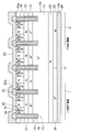
- the semiconductor device has a semiconductor substrate 10 in which an IGBT region 1 having an IGBT (abbreviation for Insulated Gate Bipolar Transistor) element and an FWD region 2 having an FWD element (abbreviation for Free Wheeling Diode) are common. It is formed and configured in. That is, the semiconductor device of this embodiment is RC (abbreviation of Reverse Conducting) -IGBT.
- the portion on the collector layer 24 located on the other surface 10b of the semiconductor substrate 10 is defined as the IGBT region 1, and is located on the other surface 10b of the semiconductor substrate 10.
- the portion on the cathode layer 25 is the FWD region 2.
- the semiconductor device has a semiconductor substrate 10 constituting an N-type drift layer 11.
- the semiconductor substrate 10 is composed of a silicon substrate.
- a P - type electric field relaxation region 12 having a lower impurity concentration than the drift layer 11 and an N-type barrier region 13 having a higher impurity concentration than the drift layer 11 are formed from the drift layer 11 side. It is formed in order.
- a P-type base layer 14 having a higher impurity concentration than the electric field relaxation region 12 is formed on the barrier region 13.
- the top of the drift layer 11 is one side 10a of the semiconductor substrate 10.
- a plurality of trenches 15 are formed on the semiconductor substrate 10 so as to pass through the base layer 14, the barrier region 13, and the electric field relaxation region 12 from the one surface 10a side to reach the drift layer 11.
- the base layer 14, the barrier region 13, and the electric field relaxation region 12 are separated into a plurality of parts by the trench 15.
- the plurality of trenches 15 are formed in the IGBT region 1 and the FWD region 2, respectively.
- the plurality of trenches 15 are formed in a striped shape with one direction intersecting the arrangement direction of the IGBT region 1 and the FWD region 2 as the longitudinal direction (that is, the depth direction of the paper surface in FIG. 1). ..
- Each trench 15 is embedded by a gate insulating film 16 formed so as to cover the wall surface of each trench 15 and a gate electrode 17 formed of polysilicon or the like formed on the gate insulating film 16. .. This constitutes a trench gate structure.
- the gate electrode 17 formed in the IGBT region 1 is connected to a gate driver or the like via a gate pad or the like (not shown), and a predetermined voltage is applied. Further, the gate electrode 17 formed in the FWD region 2 is maintained at a predetermined potential. For example, the gate electrode 17 formed in the FWD region 2 is connected to the upper electrode 22 described later and has the same potential as the upper electrode 22.
- the base layer 14 is formed with an emitter region 18, a contact region 19, and a pillar region 20.
- the emitter region 18 has an N + type having a higher impurity concentration than the drift layer 11, and is formed on the surface layer of the base layer 14.
- the emitter region 18 is formed so as to be terminated in the base layer 14 and to be in contact with the side surface of the trench 15. More specifically, the emitter region 18 extends in a rod shape along the longitudinal direction of the trench 15 so as to be in contact with the side surface of the trench 15 in the region between the adjacent trenches 15, and terminates inside the tip of the trench 15. It is said to be a structure.
- the contact region 19 is a P + type having a higher impurity concentration than the base layer 14, and is formed on the surface layer portion of the base layer 14. Specifically, the contact region 19 is formed so as to be terminated in the base layer 14 and sandwiched between the two emitter regions 18. More specifically, the contact region 19 extends in a rod shape along the longitudinal direction of the trench 15 so as to be in contact with the emitter region 18.
- the pillar region 20 has an impurity concentration similar to that of the barrier region 13, and is formed so as to penetrate the contact region 19 and the base layer 14 and reach the barrier region 13. That is, the pillar region 20 is formed so as to be connected to the barrier region 13.
- An interlayer insulating film 21 made of BPSG (abbreviation of Borophosphosilicate Glass) or the like is formed on one surface 10a of the semiconductor substrate 10.
- the interlayer insulating film 21 is formed with a contact hole 21a that exposes the emitter region 18, the contact region 19, and the pillar region 20.
- An upper electrode 22 corresponding to a metal film is formed on the interlayer insulating film 21.
- the upper electrode 22 is ohmic-bonded to the emitter region 18 and the contact region 19 and Schottky-bonded to the pillar region 20 through the contact hole 21a formed in the interlayer insulating film 21 in the IGBT region 1 and the FWD region 2. ing. That is, the upper electrode 22 of the present embodiment is configured to include both a Schottky-bonded portion and an ohmic-bonded portion. Since the upper electrode 22 is formed in this way, the upper electrode 22 functions as an emitter electrode in the IGBT region 1 and as an anode electrode in the FWD region 2. The specific configuration of the upper electrode 22 will be described later.
- An N-type field stop layer (hereinafter referred to as an FS layer) 23 having a higher carrier concentration than the drift layer 11 is formed on the side of the drift layer 11 opposite to the base layer 14 side. That is, the FS layer 23 is formed on the other surface 10b side of the semiconductor substrate 10.
- a P + type collector layer 24 is formed on the side opposite to the drift layer 11 with the FS layer 23 interposed therebetween, and in the FWD region 2, an N + type collector layer 24 is formed on the opposite side of the drift layer 11 with the FS layer 23 interposed therebetween.
- the cathode layer 25 is formed.
- the IGBT region 1 and the FWD region 2 are partitioned by whether the layer located on the other surface 10b of the semiconductor substrate 10 is the collector layer 24 or the cathode layer 25. That is, in the semiconductor device of the present embodiment, the portion on the collector layer 24 is the IGBT region 1, and the portion on the cathode layer 25 is the FWD region 2.
- a lower electrode 26 electrically connected to the collector layer 24 and the cathode layer 25 is formed on the side opposite to the drift layer 11 with the collector layer 24 and the cathode layer 25 interposed therebetween.
- a lower electrode 26 that functions as a collector electrode in the IGBT region 1 and a cathode electrode in the FWD region 2 is formed on the other surface 10b of the semiconductor substrate 10.
- the semiconductor device of the present embodiment comprises an IGBT element having a base layer 14 as a base, an emitter region 18 as an emitter, and a collector layer 24 as a collector in the IGBT region 1. .. Further, in the FWD region 2, a PN-junctioned FWD element is configured with the base layer as an anode and the drift layer 11, the FS layer 23, and the cathode layer 25 as cathodes.
- N-type, N + -type, and N - type correspond to the first conductive type
- P-type, P - type, and P + type correspond to the second conductive type
- the semiconductor substrate 10 is configured as described above, so that the semiconductor substrate 10 has a collector layer 24, a cathode layer 25, an FS layer 23, a drift layer 11, an electric field relaxation region 12, a barrier region 13, and a base layer 14.
- the emitter region 18, the contact region 19, and the pillar region 20 are included.
- the upper electrode 22 of the present embodiment is made of an aluminum alloy in which an element is added to aluminum, and is made of, for example, AlSi, AlCu, AlSiCu, or the like. Further, in the present embodiment, the upper electrode 22 is formed by a sputtering method as described later, but the added element has a solid solution solubility or higher with respect to the temperature at the time of sputtering so that alloy spikes are less likely to occur. Has been added.
- the upper electrode 22 of the present embodiment is made of a thick film having a thickness of 3 ⁇ m or more so as not to be easily broken when a probe needle or the like for inspecting the characteristics of the semiconductor device is brought into contact with the upper electrode 22.
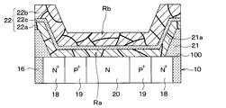
- the upper electrode 22 is configured by laminating a lower metal layer 22a and an upper metal layer 22b from the semiconductor substrate 10 side.
- the lower metal layer 22a of the upper electrode 22 is ohmic-bonded or Schottky-bonded to the semiconductor substrate 10.
- the lower metal layer 22a is ohmic-bonded to the emitter region 18 and the contact region 19, and is Schottky-bonded to the pillar region 20.
- the upper electrode 22 of the present embodiment has an insulating film 22c arranged between the lower metal layer 22a and the upper metal layer 22b.
- the insulating film 22c which will be described in detail later, is a natural oxide film formed by forming a lower metal layer 22a by a sputtering method and then exposing it to the atmosphere, and has an extremely thin thickness of 10 nm or less. There is. Therefore, the lower metal layer 22a and the upper metal layer 22b are electrically connected by the tunnel effect. In FIG. 2, the insulating film 22c is exaggerated to facilitate understanding of the insulating film 22c.
- the upper electrode 22 is in a state in which the particles Ra constituting the lower metal layer 22a and the particles Rb constituting the upper metal layer 22b are separated. That is, the grain boundaries of the particles Ra constituting the lower metal layer 22a and the grain boundaries of the particles Rb constituting the upper metal layer 22b are not connected and are in a separated state. In other words, the grain boundaries of the particles Ra constituting the lower metal layer 22a and the grain boundaries of the particles Rb constituting the upper metal layer 22b are in a state of being terminated in each layer. Therefore, even if nodules are generated in the lower metal layer 22a, the nodules are terminated in the lower metal layer 22a and do not protrude into the upper metal layer 22b.
- nodules may be deposited inside as described above.
- the Schottky barrier may fluctuate due to the stress caused by the nodule, and a leak defect may occur.
- the nodules tend to grow along the thickness direction of the upper electrode 22. That is, the stress caused by the nodules tends to depend on the length of the upper electrode 22 in the nodules along the thickness direction.
- the upper electrode 22 of the present embodiment is in a state in which the nodules in the lower metal layer 22a do not protrude into the upper metal layer 22b as described above. Therefore, the stress caused by the nodules depends on the thickness of the lower metal layer 22a.
- the thickness here is the length along the stacking direction of the lower metal layer 22a and the upper metal layer 22b.
- the present inventors diligently examined the relationship between the thickness of the lower metal layer 22a and the leak defect rate, and obtained the results shown in FIG. As shown in FIG. 3, it is confirmed that the leak defect rate starts to occur when the lower metal layer 22a is 1.5 ⁇ m or more, and sharply increases when the lower metal layer 22a is 2.6 ⁇ m or more. Therefore, in the present embodiment, the thickness of the lower metal layer 22a is set to 2.6 ⁇ m or less. In this case, preferably, the thickness of the lower metal layer 22a is 1.5 ⁇ m or less, so that the leak defect rate can be sufficiently reduced.
- the PN junction formed between the base layer 14 and the drift layer 11 becomes a reverse conduction state and a depletion layer is formed.
- a low level (for example, 0V) voltage lower than the threshold voltage Vth of the insulated gate structure is applied to the gate electrode 17, no current flows between the upper electrode 22 and the lower electrode 26.
- a high level voltage equal to or higher than the threshold voltage Vth of the insulated gate structure is applied to the gate electrode 17 of the IGBT region 1 with a voltage higher than that of the upper electrode 22 applied to the lower electrode 26. Is applied.
- an inversion layer is formed in the portion of the base layer 14 in contact with the trench 15 in which the gate electrode 17 is arranged.
- electrons are supplied from the emitter region 18 to the drift layer 11 via the inversion layer, so that holes are supplied to the drift layer 11 from the collector layer 24, and the resistance value of the drift layer 11 is supplied by conductivity modulation. Turns on when the value drops.
- the IGBT element when the IGBT element is turned off and the FWD element is turned on (that is, the FWD element is operated by a diode), the voltage applied to the upper electrode 22 and the lower electrode 26 is switched, and the lower part is transferred to the upper electrode 22.
- a forward voltage is applied to apply a voltage higher than that of the electrode 26.
- the Schottky junction between the upper electrode 22 and the pillar region 20 is turned on.
- electrons flow from the lower electrode 26 toward the upper electrode 22 via the cathode layer 25, the drift layer 11, the electric field relaxation region 12, the barrier region 13, and the pillar region 20, and the potential of the barrier region 13 is the potential of the upper electrode 22.
- the potential is close to the potential.
- the Schottky junction is turned on first, so that the timing at which the PN junction is turned on is delayed. As a result, the inflow of holes into the drift layer 11 is suppressed. Therefore, when the FWD element recovers, the recovery current can be reduced and the recovery loss can be reduced.
- the parasitic diode is also formed in the IGBT region 1 by the PN junction between the base layer 14 and the barrier region 13.
- the barrier region 13 of the IGBT element in this PN junction is connected to the upper electrode 22 via the pillar region 20. Therefore, as described above, when the potential of the upper electrode 22 rises, a current first flows in the pillar region 20. After that, when the forward voltage rises further, the PN junction constituting the parasitic diode is turned on. As described above, even within the IGBT region 1, the timing at which the PN junction is turned on is delayed, and the inflow of holes into the drift layer 11 is suppressed. This also suppresses the recovery current.
- the electric field relaxation region 12 is formed between the barrier region 13 and the drift layer 11. Therefore, as compared with the case where the electric field relaxation region 12 is not formed, the PN junction formed between the electric field relaxation region 12 and the drift layer 11 makes it difficult for the equipotential lines to enter between the trenches 15. .. Therefore, the withstand voltage can be improved.
- a semiconductor substrate 10 having a base layer 14, an emitter region 18, a contact region 19, a pillar region 20, and the like formed by performing a predetermined semiconductor manufacturing process is prepared.
- the interlayer insulating film 21 is formed on one surface 10a of the semiconductor substrate 10, and the contact hole 21a is formed in the interlayer insulating film 21.
- the semiconductor substrate 10 is arranged in the sputtering apparatus, and the lower metal layer 22a is formed by the sputtering method.
- the lower metal layer 22a is configured by adding an element having a solid solubility limit or higher with respect to the temperature at the time of sputtering so that alloy spikes are less likely to occur. Therefore, it is not necessary to form a barrier metal or the like because alloy spikes are less likely to occur at the portion where the upper electrode 22 is ohmic-bonded to the semiconductor substrate 10.
- the upper electrode 22 having a portion to be ohmic-bonded to the semiconductor substrate 10 and a portion to be Schottky-bonded can be formed in the same process without forming a barrier metal or the like.
- the lower metal layer 22a is formed so as to have a thickness of 2.6 ⁇ m or less as described above.
- the semiconductor substrate 10 is taken out from the sputtering apparatus and exposed to the atmosphere to form the insulating film 22c on the lower metal layer 22a.
- the semiconductor substrate 10 is arranged in the sputtering apparatus again, and the same sputtering method as that for the lower metal layer 22a is performed to form the upper metal layer 22b. As a result, the upper electrode 22 of the present embodiment is formed.
- the grain boundaries of the particles Ra constituting the lower metal layer 22a may protrude into the upper metal layer 22b in the upper metal layer 22b. No. That is, it is suppressed that the nodules generated in the lower metal layer 22a increase in the thickness direction of the upper electrode 22. Therefore, a semiconductor device in which leak defects are unlikely to occur is manufactured.
- the upper electrode 22 is configured by laminating the upper metal layer 22b on the lower metal layer 22a.
- the grain boundaries in the lower metal layer 22a and the grain boundaries in the upper metal layer 22b are not connected and are separated.
- the thickness of the lower metal layer 22a is set to 2.6 ⁇ m or less. Therefore, even if nodules are formed in the portion of the lower metal layer 22a to be Schottky-bonded, it is possible to suppress an increase in the leak defect rate.
- the thickness of the lower metal layer 22a is set to 1.5 ⁇ m or less. Therefore, even if the size of the semiconductor substrate 10 is increased in the plane direction, it is possible to suppress an increase in the leak defect rate, and it is possible to improve the degree of freedom in designing the semiconductor device.
- the lower metal layer 22a when the lower metal layer 22a is formed, an element having a solid solution solubility or higher at the temperature at the time of sputtering is added. Therefore, it is possible to suppress the occurrence of alloy spikes, and the lower metal layer 22a can be ohmic-bonded to the semiconductor substrate 10 without forming a barrier metal. That is, the lower metal layer 22a having the ohmic-bonded portion and the Schottky-bonded portion can be formed in the same process without forming the barrier metal.
- the lower metal layer 22a is formed by adding an element having a solid solubility limit or higher at the temperature at the time of sputtering, nodules are likely to be generated, but the thickness of the lower metal layer 22a is 2.6 ⁇ m or less. , The increase in leak defect rate is suppressed.
- the average particle size of the particles Rb constituting the upper metal layer 22b is smaller than the average particle size of the particles Ra constituting the lower metal layer 22a as compared with the first embodiment.
- Others are the same as those in the first embodiment, and thus description thereof will be omitted here.
- the average particle size of the particles Rb constituting the upper metal layer 22b is made smaller than the average particle size of the particles Ra constituting the lower metal layer 22a. It is said that it has a structure.
- Such an upper electrode 22 is manufactured as follows.
- the sputtering method is performed at a high temperature of 400 ° C. or higher.
- the sputtering method is performed at a temperature lower than the sputtering method for forming the lower metal layer 22a.
- a sputtering method is performed at about 300 to 350 ° C.
- the average particle size of the particles Rb constituting the upper metal layer 22b is the particles constituting the lower metal layer 22a. It is smaller than the average particle size of Ra.
- the average particle size of the particles Rb constituting the upper metal layer 22b is smaller than the average particle size of the particles Ra constituting the lower metal layer 22a. Therefore, as compared with the case where the average particle size of the particles Rb constituting the upper metal layer 22b is equal to or larger than the average particle size of the particles Ra constituting the lower metal layer 22a, the lower metal layer 22a in the upper metal layer 22b On the surface opposite to the side, the grain boundary step becomes small. Therefore, when performing a visual inspection, it is possible to reduce the possibility that the grain boundary step is erroneously determined as a defect or a foreign substance.
- the third embodiment will be described.
- the insulating film 22c is not arranged between the upper metal layer 22b and the lower metal layer 22a as compared with the first embodiment. Others are the same as those in the first embodiment, and thus description thereof will be omitted here.
- the upper electrode 22 has a configuration in which the insulating film 22c is not arranged between the lower metal layer 22a and the upper metal layer 22b.
- Such an upper electrode 22 is manufactured as follows.
- an inert gas such as argon is introduced into the sputtering apparatus, and the lower metal layer 22a is cooled to form the lower metal layer 22a.
- the growth of the particle Ra is completely stopped.
- the process of FIG. 4C is performed without performing the process of FIG. 4B.
- the upper metal layer 22b is composed of particles Rb different from the particles Ra constituting the lower metal layer 22a. Therefore, the particles Ra constituting the lower metal layer 22a and the particles Rb constituting the upper metal layer 22b are separated from each other.
- the particles Ra constituting the lower metal layer 22a and the particles Rb constituting the upper metal layer 22b are formed. If it is in a divided state, the same effect as that of the first embodiment can be obtained.
- the semiconductor device has the IGBT region 1 and the FWD region 2, but if the semiconductor device has a Schottky-bonded portion, it has only one of the IGBT region 1 and the FWD region 2. It may be configured. Further, the upper electrode 22 may be configured to have only a portion to be Schottky-bonded, or may not have a portion to be ohmic-bonded. Further, in each of the above embodiments, the composition of the lower metal layer 22a and the composition of the upper metal layer 22b may be different.
- each of the above embodiments can be combined.
- the second embodiment is combined with the third embodiment so that the average particle size of the particles Rb constituting the upper metal layer 22b is smaller than the average particle size of the particles Ra constituting the lower metal layer 22a. May be good.
- a combination of the above embodiments may be combined.
Landscapes
- Electrodes Of Semiconductors (AREA)
- Engineering & Computer Science (AREA)
- Manufacturing & Machinery (AREA)
- Metal-Oxide And Bipolar Metal-Oxide Semiconductor Integrated Circuits (AREA)
- Insulated Gate Type Field-Effect Transistor (AREA)
Priority Applications (3)
| Application Number | Priority Date | Filing Date | Title |
|---|---|---|---|
| CN202180045017.7A CN115735264A (zh) | 2020-06-26 | 2021-06-23 | 半导体装置及其制造方法 |
| US18/065,916 US12581716B2 (en) | 2020-06-26 | 2022-12-14 | Semiconductor device with metal film on semiconductor substrate and method of manufacturing the same |
| US19/433,259 US20260123017A1 (en) | 2020-06-26 | 2025-12-26 | Semiconductor device |
Applications Claiming Priority (2)
| Application Number | Priority Date | Filing Date | Title |
|---|---|---|---|
| JP2020110888A JP2022007763A (ja) | 2020-06-26 | 2020-06-26 | 半導体装置およびその製造方法 |
| JP2020-110888 | 2020-06-26 |
Related Child Applications (1)
| Application Number | Title | Priority Date | Filing Date |
|---|---|---|---|
| US18/065,916 Continuation US12581716B2 (en) | 2020-06-26 | 2022-12-14 | Semiconductor device with metal film on semiconductor substrate and method of manufacturing the same |
Publications (1)
| Publication Number | Publication Date |
|---|---|
| WO2021261521A1 true WO2021261521A1 (ja) | 2021-12-30 |
Family
ID=79281330
Family Applications (1)
| Application Number | Title | Priority Date | Filing Date |
|---|---|---|---|
| PCT/JP2021/023793 Ceased WO2021261521A1 (ja) | 2020-06-26 | 2021-06-23 | 半導体装置およびその製造方法 |
Country Status (4)
| Country | Link |
|---|---|
| US (2) | US12581716B2 (https=) |
| JP (1) | JP2022007763A (https=) |
| CN (1) | CN115735264A (https=) |
| WO (1) | WO2021261521A1 (https=) |
Cited By (1)
| Publication number | Priority date | Publication date | Assignee | Title |
|---|---|---|---|---|
| WO2026048279A1 (ja) * | 2024-08-28 | 2026-03-05 | 株式会社デンソー | 半導体素子 |
Families Citing this family (2)
| Publication number | Priority date | Publication date | Assignee | Title |
|---|---|---|---|---|
| JP2024098458A (ja) * | 2023-01-10 | 2024-07-23 | 富士電機株式会社 | 半導体装置 |
| CN116632053B (zh) * | 2023-07-25 | 2024-01-30 | 深圳市美浦森半导体有限公司 | 一种rc-igbt器件的控制方法 |
Citations (7)
| Publication number | Priority date | Publication date | Assignee | Title |
|---|---|---|---|---|
| JPH01238162A (ja) * | 1988-03-18 | 1989-09-22 | Nec Corp | 半導体装置 |
| JPH0376030B2 (https=) * | 1981-09-11 | 1991-12-04 | Fujitsu Ltd | |
| JPH08124877A (ja) * | 1994-10-24 | 1996-05-17 | Sanyo Electric Co Ltd | 半導体集積回路の製造方法 |
| JP2006351717A (ja) * | 2005-06-14 | 2006-12-28 | Toyota Motor Corp | 半導体装置及びその製造方法 |
| JP2015216200A (ja) * | 2014-05-09 | 2015-12-03 | 株式会社豊田中央研究所 | 半導体装置 |
| JP2017135283A (ja) * | 2016-01-28 | 2017-08-03 | ローム株式会社 | 半導体装置および半導体装置の製造方法 |
| JP2019145667A (ja) * | 2018-02-21 | 2019-08-29 | ルネサスエレクトロニクス株式会社 | 半導体装置および半導体装置の製造方法 |
Family Cites Families (13)
| Publication number | Priority date | Publication date | Assignee | Title |
|---|---|---|---|---|
| JPH0638493B2 (ja) | 1984-02-15 | 1994-05-18 | 三洋電機株式会社 | 半導体集積回路の製造方法 |
| JPS6312952A (ja) | 1986-07-04 | 1988-01-20 | Mitsubishi Heavy Ind Ltd | ガスクロマトグラフ用保温ガスサンプラ |
| EP1819202B1 (en) * | 2006-02-10 | 2011-04-06 | Semiconductor Energy Laboratory Co., Ltd. | Semiconductor device and manufacturing method thereof |
| JP2008021701A (ja) * | 2006-07-11 | 2008-01-31 | Sharp Corp | 半導体装置及びその製造方法 |
| JP5549118B2 (ja) | 2009-05-27 | 2014-07-16 | トヨタ自動車株式会社 | 半導体装置の製造方法 |
| WO2014006695A1 (ja) * | 2012-07-03 | 2014-01-09 | 新電元工業株式会社 | 半導体装置 |
| JP5772926B2 (ja) * | 2013-01-07 | 2015-09-02 | 株式会社デンソー | 半導体装置 |
| JP2016054250A (ja) * | 2014-09-04 | 2016-04-14 | 豊田合成株式会社 | 半導体装置、製造方法、方法 |
| JP2016099127A (ja) * | 2014-11-18 | 2016-05-30 | 富士電機株式会社 | パワー半導体モジュールの製造方法及びその中間組立ユニット |
| JP2016143804A (ja) * | 2015-02-03 | 2016-08-08 | トヨタ自動車株式会社 | 半導体装置 |
| JP6616691B2 (ja) * | 2016-01-18 | 2019-12-04 | ルネサスエレクトロニクス株式会社 | 半導体装置およびその製造方法 |
| JP6719090B2 (ja) | 2016-12-19 | 2020-07-08 | パナソニックIpマネジメント株式会社 | 半導体素子 |
| JP6773577B2 (ja) | 2017-02-01 | 2020-10-21 | トヨタ自動車株式会社 | 半導体装置 |
-
2020
- 2020-06-26 JP JP2020110888A patent/JP2022007763A/ja active Pending
-
2021
- 2021-06-23 CN CN202180045017.7A patent/CN115735264A/zh active Pending
- 2021-06-23 WO PCT/JP2021/023793 patent/WO2021261521A1/ja not_active Ceased
-
2022
- 2022-12-14 US US18/065,916 patent/US12581716B2/en active Active
-
2025
- 2025-12-26 US US19/433,259 patent/US20260123017A1/en active Pending
Patent Citations (7)
| Publication number | Priority date | Publication date | Assignee | Title |
|---|---|---|---|---|
| JPH0376030B2 (https=) * | 1981-09-11 | 1991-12-04 | Fujitsu Ltd | |
| JPH01238162A (ja) * | 1988-03-18 | 1989-09-22 | Nec Corp | 半導体装置 |
| JPH08124877A (ja) * | 1994-10-24 | 1996-05-17 | Sanyo Electric Co Ltd | 半導体集積回路の製造方法 |
| JP2006351717A (ja) * | 2005-06-14 | 2006-12-28 | Toyota Motor Corp | 半導体装置及びその製造方法 |
| JP2015216200A (ja) * | 2014-05-09 | 2015-12-03 | 株式会社豊田中央研究所 | 半導体装置 |
| JP2017135283A (ja) * | 2016-01-28 | 2017-08-03 | ローム株式会社 | 半導体装置および半導体装置の製造方法 |
| JP2019145667A (ja) * | 2018-02-21 | 2019-08-29 | ルネサスエレクトロニクス株式会社 | 半導体装置および半導体装置の製造方法 |
Cited By (1)
| Publication number | Priority date | Publication date | Assignee | Title |
|---|---|---|---|---|
| WO2026048279A1 (ja) * | 2024-08-28 | 2026-03-05 | 株式会社デンソー | 半導体素子 |
Also Published As
| Publication number | Publication date |
|---|---|
| CN115735264A (zh) | 2023-03-03 |
| US20260123017A1 (en) | 2026-04-30 |
| US12581716B2 (en) | 2026-03-17 |
| US20230125063A1 (en) | 2023-04-20 |
| JP2022007763A (ja) | 2022-01-13 |
Similar Documents
| Publication | Publication Date | Title |
|---|---|---|
| US10879388B2 (en) | Methods of reducing the electrical and thermal resistance of SiC substrates and device made thereby | |
| JP4492735B2 (ja) | 半導体装置及び半導体装置の製造方法 | |
| US8362519B2 (en) | Semiconductor device | |
| CN107039438B (zh) | 半导体装置 | |
| CN102473723B (zh) | 功率用半导体装置及其制造方法 | |
| JP6304445B2 (ja) | 半導体装置の製造方法 | |
| US12581716B2 (en) | Semiconductor device with metal film on semiconductor substrate and method of manufacturing the same | |
| CN105849912A (zh) | 半导体装置及其制造方法 | |
| JP7283036B2 (ja) | 半導体装置および製造方法 | |
| CN109686789B (zh) | 半导体装置 | |
| CN106409897B (zh) | 半导体装置及其制造方法 | |
| CN105556647B (zh) | 半导体装置及其制造方法 | |
| CN113614883B (zh) | 半导体装置 | |
| US20160163806A1 (en) | Semiconductor device and method for manufacturing the semiconductor device | |
| JP2016201498A (ja) | ダイオード | |
| CN119108283B (zh) | 半导体器件 | |
| JP2006332199A (ja) | SiC半導体装置 | |
| CN109997215A (zh) | 半导体装置的制造方法 | |
| WO2021070252A1 (ja) | 半導体装置 | |
| JPWO2021038699A1 (ja) | 半導体装置とその製造方法 | |
| JP2021093480A (ja) | 半導体装置 | |
| CN120167138A (zh) | 半导体装置 | |
| CN115552634A (zh) | 半导体装置以及其制造方法 | |
| JP2026059187A (ja) | 半導体装置および半導体装置の製造方法 | |
| JP2025070569A (ja) | 半導体装置 |
Legal Events
| Date | Code | Title | Description |
|---|---|---|---|
| 121 | Ep: the epo has been informed by wipo that ep was designated in this application |
Ref document number: 21829423 Country of ref document: EP Kind code of ref document: A1 |
|
| NENP | Non-entry into the national phase |
Ref country code: DE |
|
| 122 | Ep: pct application non-entry in european phase |
Ref document number: 21829423 Country of ref document: EP Kind code of ref document: A1 |