WO2021261521A1 - Semiconductor device and manufacturing method therefor - Google Patents
Semiconductor device and manufacturing method therefor Download PDFInfo
- Publication number
- WO2021261521A1 WO2021261521A1 PCT/JP2021/023793 JP2021023793W WO2021261521A1 WO 2021261521 A1 WO2021261521 A1 WO 2021261521A1 JP 2021023793 W JP2021023793 W JP 2021023793W WO 2021261521 A1 WO2021261521 A1 WO 2021261521A1
- Authority
- WO
- WIPO (PCT)
- Prior art keywords
- metal layer
- lower metal
- semiconductor substrate
- layer
- region
- Prior art date
Links
- 239000004065 semiconductor Substances 0.000 title claims abstract description 104
- 238000004519 manufacturing process Methods 0.000 title claims description 15
- 229910052751 metal Inorganic materials 0.000 claims abstract description 164
- 239000002184 metal Substances 0.000 claims abstract description 164
- 239000000758 substrate Substances 0.000 claims abstract description 60
- 229910000838 Al alloy Inorganic materials 0.000 claims abstract description 8
- 229910052782 aluminium Inorganic materials 0.000 claims abstract description 6
- XAGFODPZIPBFFR-UHFFFAOYSA-N aluminium Chemical compound [Al] XAGFODPZIPBFFR-UHFFFAOYSA-N 0.000 claims abstract description 6
- 239000002245 particle Substances 0.000 claims description 48
- 238000004544 sputter deposition Methods 0.000 claims description 21
- 238000000034 method Methods 0.000 claims description 12
- 238000010030 laminating Methods 0.000 claims description 4
- 239000007787 solid Substances 0.000 claims description 3
- 239000010410 layer Substances 0.000 description 180
- 230000004888 barrier function Effects 0.000 description 22
- 230000007547 defect Effects 0.000 description 17
- 239000011229 interlayer Substances 0.000 description 11
- 230000005684 electric field Effects 0.000 description 9
- 239000012535 impurity Substances 0.000 description 6
- 229910045601 alloy Inorganic materials 0.000 description 4
- 239000000956 alloy Substances 0.000 description 4
- XUIMIQQOPSSXEZ-UHFFFAOYSA-N Silicon Chemical compound [Si] XUIMIQQOPSSXEZ-UHFFFAOYSA-N 0.000 description 3
- 238000011084 recovery Methods 0.000 description 3
- 229910052710 silicon Inorganic materials 0.000 description 3
- 239000010703 silicon Substances 0.000 description 3
- XKRFYHLGVUSROY-UHFFFAOYSA-N Argon Chemical compound [Ar] XKRFYHLGVUSROY-UHFFFAOYSA-N 0.000 description 2
- 239000005380 borophosphosilicate glass Substances 0.000 description 2
- 230000003111 delayed effect Effects 0.000 description 2
- 230000000694 effects Effects 0.000 description 2
- 239000000203 mixture Substances 0.000 description 2
- 230000003071 parasitic effect Effects 0.000 description 2
- 239000006104 solid solution Substances 0.000 description 2
- 239000002344 surface layer Substances 0.000 description 2
- 229910016570 AlCu Inorganic materials 0.000 description 1
- 229910000789 Aluminium-silicon alloy Inorganic materials 0.000 description 1
- RYGMFSIKBFXOCR-UHFFFAOYSA-N Copper Chemical compound [Cu] RYGMFSIKBFXOCR-UHFFFAOYSA-N 0.000 description 1
- 229910052786 argon Inorganic materials 0.000 description 1
- 229910052802 copper Inorganic materials 0.000 description 1
- 239000010949 copper Substances 0.000 description 1
- 239000011261 inert gas Substances 0.000 description 1
- 229910021420 polycrystalline silicon Inorganic materials 0.000 description 1
- 229920005591 polysilicon Polymers 0.000 description 1
- 239000000523 sample Substances 0.000 description 1
- 239000000126 substance Substances 0.000 description 1
- 238000011179 visual inspection Methods 0.000 description 1
Images


Classifications
-
- H—ELECTRICITY
- H01—ELECTRIC ELEMENTS
- H01L—SEMICONDUCTOR DEVICES NOT COVERED BY CLASS H10
- H01L29/00—Semiconductor devices adapted for rectifying, amplifying, oscillating or switching, or capacitors or resistors with at least one potential-jump barrier or surface barrier, e.g. PN junction depletion layer or carrier concentration layer; Details of semiconductor bodies or of electrodes thereof ; Multistep manufacturing processes therefor
- H01L29/40—Electrodes ; Multistep manufacturing processes therefor
- H01L29/43—Electrodes ; Multistep manufacturing processes therefor characterised by the materials of which they are formed
- H01L29/47—Schottky barrier electrodes
-
- H—ELECTRICITY
- H01—ELECTRIC ELEMENTS
- H01L—SEMICONDUCTOR DEVICES NOT COVERED BY CLASS H10
- H01L29/00—Semiconductor devices adapted for rectifying, amplifying, oscillating or switching, or capacitors or resistors with at least one potential-jump barrier or surface barrier, e.g. PN junction depletion layer or carrier concentration layer; Details of semiconductor bodies or of electrodes thereof ; Multistep manufacturing processes therefor
- H01L29/66—Types of semiconductor device ; Multistep manufacturing processes therefor
- H01L29/86—Types of semiconductor device ; Multistep manufacturing processes therefor controllable only by variation of the electric current supplied, or only the electric potential applied, to one or more of the electrodes carrying the current to be rectified, amplified, oscillated or switched
- H01L29/861—Diodes
- H01L29/872—Schottky diodes
-
- H—ELECTRICITY
- H01—ELECTRIC ELEMENTS
- H01L—SEMICONDUCTOR DEVICES NOT COVERED BY CLASS H10
- H01L21/00—Processes or apparatus adapted for the manufacture or treatment of semiconductor or solid state devices or of parts thereof
- H01L21/02—Manufacture or treatment of semiconductor devices or of parts thereof
- H01L21/04—Manufacture or treatment of semiconductor devices or of parts thereof the devices having at least one potential-jump barrier or surface barrier, e.g. PN junction, depletion layer or carrier concentration layer
- H01L21/18—Manufacture or treatment of semiconductor devices or of parts thereof the devices having at least one potential-jump barrier or surface barrier, e.g. PN junction, depletion layer or carrier concentration layer the devices having semiconductor bodies comprising elements of Group IV of the Periodic System or AIIIBV compounds with or without impurities, e.g. doping materials
- H01L21/28—Manufacture of electrodes on semiconductor bodies using processes or apparatus not provided for in groups H01L21/20 - H01L21/268
-
- H—ELECTRICITY
- H01—ELECTRIC ELEMENTS
- H01L—SEMICONDUCTOR DEVICES NOT COVERED BY CLASS H10
- H01L27/00—Devices consisting of a plurality of semiconductor or other solid-state components formed in or on a common substrate
- H01L27/02—Devices consisting of a plurality of semiconductor or other solid-state components formed in or on a common substrate including semiconductor components specially adapted for rectifying, oscillating, amplifying or switching and having at least one potential-jump barrier or surface barrier; including integrated passive circuit elements with at least one potential-jump barrier or surface barrier
- H01L27/04—Devices consisting of a plurality of semiconductor or other solid-state components formed in or on a common substrate including semiconductor components specially adapted for rectifying, oscillating, amplifying or switching and having at least one potential-jump barrier or surface barrier; including integrated passive circuit elements with at least one potential-jump barrier or surface barrier the substrate being a semiconductor body
- H01L27/06—Devices consisting of a plurality of semiconductor or other solid-state components formed in or on a common substrate including semiconductor components specially adapted for rectifying, oscillating, amplifying or switching and having at least one potential-jump barrier or surface barrier; including integrated passive circuit elements with at least one potential-jump barrier or surface barrier the substrate being a semiconductor body including a plurality of individual components in a non-repetitive configuration
- H01L27/0611—Devices consisting of a plurality of semiconductor or other solid-state components formed in or on a common substrate including semiconductor components specially adapted for rectifying, oscillating, amplifying or switching and having at least one potential-jump barrier or surface barrier; including integrated passive circuit elements with at least one potential-jump barrier or surface barrier the substrate being a semiconductor body including a plurality of individual components in a non-repetitive configuration integrated circuits having a two-dimensional layout of components without a common active region
- H01L27/0641—Devices consisting of a plurality of semiconductor or other solid-state components formed in or on a common substrate including semiconductor components specially adapted for rectifying, oscillating, amplifying or switching and having at least one potential-jump barrier or surface barrier; including integrated passive circuit elements with at least one potential-jump barrier or surface barrier the substrate being a semiconductor body including a plurality of individual components in a non-repetitive configuration integrated circuits having a two-dimensional layout of components without a common active region without components of the field effect type
- H01L27/0647—Bipolar transistors in combination with diodes, or capacitors, or resistors, e.g. vertical bipolar transistor and bipolar lateral transistor and resistor
- H01L27/0652—Vertical bipolar transistor in combination with diodes, or capacitors, or resistors
- H01L27/0664—Vertical bipolar transistor in combination with diodes
-
- H—ELECTRICITY
- H01—ELECTRIC ELEMENTS
- H01L—SEMICONDUCTOR DEVICES NOT COVERED BY CLASS H10
- H01L29/00—Semiconductor devices adapted for rectifying, amplifying, oscillating or switching, or capacitors or resistors with at least one potential-jump barrier or surface barrier, e.g. PN junction depletion layer or carrier concentration layer; Details of semiconductor bodies or of electrodes thereof ; Multistep manufacturing processes therefor
- H01L29/02—Semiconductor bodies ; Multistep manufacturing processes therefor
- H01L29/06—Semiconductor bodies ; Multistep manufacturing processes therefor characterised by their shape; characterised by the shapes, relative sizes, or dispositions of the semiconductor regions ; characterised by the concentration or distribution of impurities within semiconductor regions
- H01L29/10—Semiconductor bodies ; Multistep manufacturing processes therefor characterised by their shape; characterised by the shapes, relative sizes, or dispositions of the semiconductor regions ; characterised by the concentration or distribution of impurities within semiconductor regions with semiconductor regions connected to an electrode not carrying current to be rectified, amplified or switched and such electrode being part of a semiconductor device which comprises three or more electrodes
- H01L29/1095—Body region, i.e. base region, of DMOS transistors or IGBTs
-
- H—ELECTRICITY
- H01—ELECTRIC ELEMENTS
- H01L—SEMICONDUCTOR DEVICES NOT COVERED BY CLASS H10
- H01L29/00—Semiconductor devices adapted for rectifying, amplifying, oscillating or switching, or capacitors or resistors with at least one potential-jump barrier or surface barrier, e.g. PN junction depletion layer or carrier concentration layer; Details of semiconductor bodies or of electrodes thereof ; Multistep manufacturing processes therefor
- H01L29/40—Electrodes ; Multistep manufacturing processes therefor
- H01L29/401—Multistep manufacturing processes
-
- H—ELECTRICITY
- H01—ELECTRIC ELEMENTS
- H01L—SEMICONDUCTOR DEVICES NOT COVERED BY CLASS H10
- H01L29/00—Semiconductor devices adapted for rectifying, amplifying, oscillating or switching, or capacitors or resistors with at least one potential-jump barrier or surface barrier, e.g. PN junction depletion layer or carrier concentration layer; Details of semiconductor bodies or of electrodes thereof ; Multistep manufacturing processes therefor
- H01L29/40—Electrodes ; Multistep manufacturing processes therefor
- H01L29/402—Field plates
- H01L29/407—Recessed field plates, e.g. trench field plates, buried field plates
-
- H—ELECTRICITY
- H01—ELECTRIC ELEMENTS
- H01L—SEMICONDUCTOR DEVICES NOT COVERED BY CLASS H10
- H01L29/00—Semiconductor devices adapted for rectifying, amplifying, oscillating or switching, or capacitors or resistors with at least one potential-jump barrier or surface barrier, e.g. PN junction depletion layer or carrier concentration layer; Details of semiconductor bodies or of electrodes thereof ; Multistep manufacturing processes therefor
- H01L29/40—Electrodes ; Multistep manufacturing processes therefor
- H01L29/41—Electrodes ; Multistep manufacturing processes therefor characterised by their shape, relative sizes or dispositions
- H01L29/417—Electrodes ; Multistep manufacturing processes therefor characterised by their shape, relative sizes or dispositions carrying the current to be rectified, amplified or switched
-
- H—ELECTRICITY
- H01—ELECTRIC ELEMENTS
- H01L—SEMICONDUCTOR DEVICES NOT COVERED BY CLASS H10
- H01L29/00—Semiconductor devices adapted for rectifying, amplifying, oscillating or switching, or capacitors or resistors with at least one potential-jump barrier or surface barrier, e.g. PN junction depletion layer or carrier concentration layer; Details of semiconductor bodies or of electrodes thereof ; Multistep manufacturing processes therefor
- H01L29/66—Types of semiconductor device ; Multistep manufacturing processes therefor
- H01L29/66007—Multistep manufacturing processes
- H01L29/66075—Multistep manufacturing processes of devices having semiconductor bodies comprising group 14 or group 13/15 materials
- H01L29/66227—Multistep manufacturing processes of devices having semiconductor bodies comprising group 14 or group 13/15 materials the devices being controllable only by the electric current supplied or the electric potential applied, to an electrode which does not carry the current to be rectified, amplified or switched, e.g. three-terminal devices
- H01L29/66409—Unipolar field-effect transistors
- H01L29/66477—Unipolar field-effect transistors with an insulated gate, i.e. MISFET
-
- H—ELECTRICITY
- H01—ELECTRIC ELEMENTS
- H01L—SEMICONDUCTOR DEVICES NOT COVERED BY CLASS H10
- H01L29/00—Semiconductor devices adapted for rectifying, amplifying, oscillating or switching, or capacitors or resistors with at least one potential-jump barrier or surface barrier, e.g. PN junction depletion layer or carrier concentration layer; Details of semiconductor bodies or of electrodes thereof ; Multistep manufacturing processes therefor
- H01L29/66—Types of semiconductor device ; Multistep manufacturing processes therefor
- H01L29/68—Types of semiconductor device ; Multistep manufacturing processes therefor controllable by only the electric current supplied, or only the electric potential applied, to an electrode which does not carry the current to be rectified, amplified or switched
- H01L29/70—Bipolar devices
- H01L29/72—Transistor-type devices, i.e. able to continuously respond to applied control signals
- H01L29/739—Transistor-type devices, i.e. able to continuously respond to applied control signals controlled by field-effect, e.g. bipolar static induction transistors [BSIT]
- H01L29/7393—Insulated gate bipolar mode transistors, i.e. IGBT; IGT; COMFET
- H01L29/7395—Vertical transistors, e.g. vertical IGBT
- H01L29/7396—Vertical transistors, e.g. vertical IGBT with a non planar surface, e.g. with a non planar gate or with a trench or recess or pillar in the surface of the emitter, base or collector region for improving current density or short circuiting the emitter and base regions
- H01L29/7397—Vertical transistors, e.g. vertical IGBT with a non planar surface, e.g. with a non planar gate or with a trench or recess or pillar in the surface of the emitter, base or collector region for improving current density or short circuiting the emitter and base regions and a gate structure lying on a slanted or vertical surface or formed in a groove, e.g. trench gate IGBT
-
- H—ELECTRICITY
- H01—ELECTRIC ELEMENTS
- H01L—SEMICONDUCTOR DEVICES NOT COVERED BY CLASS H10
- H01L29/00—Semiconductor devices adapted for rectifying, amplifying, oscillating or switching, or capacitors or resistors with at least one potential-jump barrier or surface barrier, e.g. PN junction depletion layer or carrier concentration layer; Details of semiconductor bodies or of electrodes thereof ; Multistep manufacturing processes therefor
- H01L29/66—Types of semiconductor device ; Multistep manufacturing processes therefor
- H01L29/68—Types of semiconductor device ; Multistep manufacturing processes therefor controllable by only the electric current supplied, or only the electric potential applied, to an electrode which does not carry the current to be rectified, amplified or switched
- H01L29/76—Unipolar devices, e.g. field effect transistors
- H01L29/772—Field effect transistors
- H01L29/78—Field effect transistors with field effect produced by an insulated gate
-
- H—ELECTRICITY
- H01—ELECTRIC ELEMENTS
- H01L—SEMICONDUCTOR DEVICES NOT COVERED BY CLASS H10
- H01L29/00—Semiconductor devices adapted for rectifying, amplifying, oscillating or switching, or capacitors or resistors with at least one potential-jump barrier or surface barrier, e.g. PN junction depletion layer or carrier concentration layer; Details of semiconductor bodies or of electrodes thereof ; Multistep manufacturing processes therefor
- H01L29/66—Types of semiconductor device ; Multistep manufacturing processes therefor
- H01L29/86—Types of semiconductor device ; Multistep manufacturing processes therefor controllable only by variation of the electric current supplied, or only the electric potential applied, to one or more of the electrodes carrying the current to be rectified, amplified, oscillated or switched
- H01L29/861—Diodes
-
- H—ELECTRICITY
- H01—ELECTRIC ELEMENTS
- H01L—SEMICONDUCTOR DEVICES NOT COVERED BY CLASS H10
- H01L27/00—Devices consisting of a plurality of semiconductor or other solid-state components formed in or on a common substrate
- H01L27/02—Devices consisting of a plurality of semiconductor or other solid-state components formed in or on a common substrate including semiconductor components specially adapted for rectifying, oscillating, amplifying or switching and having at least one potential-jump barrier or surface barrier; including integrated passive circuit elements with at least one potential-jump barrier or surface barrier
- H01L27/04—Devices consisting of a plurality of semiconductor or other solid-state components formed in or on a common substrate including semiconductor components specially adapted for rectifying, oscillating, amplifying or switching and having at least one potential-jump barrier or surface barrier; including integrated passive circuit elements with at least one potential-jump barrier or surface barrier the substrate being a semiconductor body
- H01L27/06—Devices consisting of a plurality of semiconductor or other solid-state components formed in or on a common substrate including semiconductor components specially adapted for rectifying, oscillating, amplifying or switching and having at least one potential-jump barrier or surface barrier; including integrated passive circuit elements with at least one potential-jump barrier or surface barrier the substrate being a semiconductor body including a plurality of individual components in a non-repetitive configuration
- H01L27/07—Devices consisting of a plurality of semiconductor or other solid-state components formed in or on a common substrate including semiconductor components specially adapted for rectifying, oscillating, amplifying or switching and having at least one potential-jump barrier or surface barrier; including integrated passive circuit elements with at least one potential-jump barrier or surface barrier the substrate being a semiconductor body including a plurality of individual components in a non-repetitive configuration the components having an active region in common
- H01L27/0705—Devices consisting of a plurality of semiconductor or other solid-state components formed in or on a common substrate including semiconductor components specially adapted for rectifying, oscillating, amplifying or switching and having at least one potential-jump barrier or surface barrier; including integrated passive circuit elements with at least one potential-jump barrier or surface barrier the substrate being a semiconductor body including a plurality of individual components in a non-repetitive configuration the components having an active region in common comprising components of the field effect type
- H01L27/0727—Devices consisting of a plurality of semiconductor or other solid-state components formed in or on a common substrate including semiconductor components specially adapted for rectifying, oscillating, amplifying or switching and having at least one potential-jump barrier or surface barrier; including integrated passive circuit elements with at least one potential-jump barrier or surface barrier the substrate being a semiconductor body including a plurality of individual components in a non-repetitive configuration the components having an active region in common comprising components of the field effect type in combination with diodes, or capacitors or resistors
Definitions
- the present disclosure relates to a semiconductor device having a Schottky junction and a method for manufacturing the same.
- Patent Document 1 proposes a semiconductor device that defines a portion to be Schottky-bonded.
- an interlayer insulating film is formed on the semiconductor substrate, and a contact hole for exposing the semiconductor substrate is formed in the interlayer insulating film. Further, the semiconductor device is formed so as to include a portion where the metal film is Schottky-bonded to the semiconductor substrate through the contact hole. In this semiconductor device, nodules formed on the metal film are likely to be formed near the opening of the interlayer insulating film, so that the portion to be Schottky-bonded is located away from the vicinity of the opening of the interlayer insulating film. ing.
- the metal film in the portion of the semiconductor substrate exposed from the interlayer insulating film, is ohmic-bonded to the semiconductor substrate on the side near the opening, and the metal film is Schottky-bonded to the semiconductor substrate on the inner edge side. It is configured to be.
- the Schottky junction is formed in a portion different from the portion where nodules are easily formed, there is a possibility that nodules are also formed at a position away from the vicinity of the opening. Then, for example, when the size of the semiconductor substrate is increased in the plane direction, the influence of nodules may not be negligible, and the leak defect rate may increase.
- An object of the present disclosure is to provide a semiconductor device capable of suppressing an increase in the leak defect rate and a method for manufacturing the same.
- the semiconductor device is composed of a semiconductor substrate, a portion formed on the semiconductor substrate and bonded to the semiconductor substrate by shot key, and an aluminum alloy in which an element is added to aluminum.
- the metal film is configured by laminating a lower metal layer arranged on the semiconductor substrate side and an upper metal layer arranged on the lower metal layer. The thickness of the lower metal layer and the upper metal layer along the stacking direction is 2.6 ⁇ m or less.
- the thickness of the lower metal layer is 2.6 ⁇ m or less, it is possible to suppress an increase in the leak defect rate.
- a method for manufacturing a semiconductor device includes preparing a semiconductor substrate and having a portion on the semiconductor substrate that is Schottky-bonded to the semiconductor substrate, and the semiconductor substrate among the metal films.
- a metal film having the lower metal layer and the upper metal layer is formed.
- a lower metal layer having a thickness of 2.6 ⁇ m or less along the stacking direction of the lower metal layer and the upper metal layer is formed.
- the lower metal layer is formed so that the thickness is 2.6 ⁇ m or less, it is possible to manufacture a semiconductor device in which the leakage defect rate is suppressed from increasing.
- FIG. 3 is an enlarged view of the vicinity of the interface between the semiconductor substrate and the upper electrode in FIG. 1. It is a figure which shows the relationship between the thickness of the lower metal layer, and the leak defect rate. It is sectional drawing which shows the manufacturing process of the upper electrode of 1st Embodiment. It is sectional drawing which shows the manufacturing process of the upper electrode following FIG. 4A. It is sectional drawing which shows the manufacturing process of the upper electrode following FIG. 4B. It is an enlarged view near the interface between the semiconductor substrate and the upper electrode in 2nd Embodiment. It is an enlarged view of the vicinity of the interface between the semiconductor substrate and the upper electrode in 3rd Embodiment.
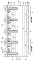
- the semiconductor device has a semiconductor substrate 10 in which an IGBT region 1 having an IGBT (abbreviation for Insulated Gate Bipolar Transistor) element and an FWD region 2 having an FWD element (abbreviation for Free Wheeling Diode) are common. It is formed and configured in. That is, the semiconductor device of this embodiment is RC (abbreviation of Reverse Conducting) -IGBT.
- the portion on the collector layer 24 located on the other surface 10b of the semiconductor substrate 10 is defined as the IGBT region 1, and is located on the other surface 10b of the semiconductor substrate 10.
- the portion on the cathode layer 25 is the FWD region 2.
- the semiconductor device has a semiconductor substrate 10 constituting an N-type drift layer 11.
- the semiconductor substrate 10 is composed of a silicon substrate.
- a P - type electric field relaxation region 12 having a lower impurity concentration than the drift layer 11 and an N-type barrier region 13 having a higher impurity concentration than the drift layer 11 are formed from the drift layer 11 side. It is formed in order.
- a P-type base layer 14 having a higher impurity concentration than the electric field relaxation region 12 is formed on the barrier region 13.
- the top of the drift layer 11 is one side 10a of the semiconductor substrate 10.
- a plurality of trenches 15 are formed on the semiconductor substrate 10 so as to pass through the base layer 14, the barrier region 13, and the electric field relaxation region 12 from the one surface 10a side to reach the drift layer 11.
- the base layer 14, the barrier region 13, and the electric field relaxation region 12 are separated into a plurality of parts by the trench 15.
- the plurality of trenches 15 are formed in the IGBT region 1 and the FWD region 2, respectively.
- the plurality of trenches 15 are formed in a striped shape with one direction intersecting the arrangement direction of the IGBT region 1 and the FWD region 2 as the longitudinal direction (that is, the depth direction of the paper surface in FIG. 1). ..
- Each trench 15 is embedded by a gate insulating film 16 formed so as to cover the wall surface of each trench 15 and a gate electrode 17 formed of polysilicon or the like formed on the gate insulating film 16. .. This constitutes a trench gate structure.
- the gate electrode 17 formed in the IGBT region 1 is connected to a gate driver or the like via a gate pad or the like (not shown), and a predetermined voltage is applied. Further, the gate electrode 17 formed in the FWD region 2 is maintained at a predetermined potential. For example, the gate electrode 17 formed in the FWD region 2 is connected to the upper electrode 22 described later and has the same potential as the upper electrode 22.
- the base layer 14 is formed with an emitter region 18, a contact region 19, and a pillar region 20.
- the emitter region 18 has an N + type having a higher impurity concentration than the drift layer 11, and is formed on the surface layer of the base layer 14.
- the emitter region 18 is formed so as to be terminated in the base layer 14 and to be in contact with the side surface of the trench 15. More specifically, the emitter region 18 extends in a rod shape along the longitudinal direction of the trench 15 so as to be in contact with the side surface of the trench 15 in the region between the adjacent trenches 15, and terminates inside the tip of the trench 15. It is said to be a structure.
- the contact region 19 is a P + type having a higher impurity concentration than the base layer 14, and is formed on the surface layer portion of the base layer 14. Specifically, the contact region 19 is formed so as to be terminated in the base layer 14 and sandwiched between the two emitter regions 18. More specifically, the contact region 19 extends in a rod shape along the longitudinal direction of the trench 15 so as to be in contact with the emitter region 18.
- the pillar region 20 has an impurity concentration similar to that of the barrier region 13, and is formed so as to penetrate the contact region 19 and the base layer 14 and reach the barrier region 13. That is, the pillar region 20 is formed so as to be connected to the barrier region 13.
- An interlayer insulating film 21 made of BPSG (abbreviation of Borophosphosilicate Glass) or the like is formed on one surface 10a of the semiconductor substrate 10.
- the interlayer insulating film 21 is formed with a contact hole 21a that exposes the emitter region 18, the contact region 19, and the pillar region 20.
- An upper electrode 22 corresponding to a metal film is formed on the interlayer insulating film 21.
- the upper electrode 22 is ohmic-bonded to the emitter region 18 and the contact region 19 and Schottky-bonded to the pillar region 20 through the contact hole 21a formed in the interlayer insulating film 21 in the IGBT region 1 and the FWD region 2. ing. That is, the upper electrode 22 of the present embodiment is configured to include both a Schottky-bonded portion and an ohmic-bonded portion. Since the upper electrode 22 is formed in this way, the upper electrode 22 functions as an emitter electrode in the IGBT region 1 and as an anode electrode in the FWD region 2. The specific configuration of the upper electrode 22 will be described later.
- An N-type field stop layer (hereinafter referred to as an FS layer) 23 having a higher carrier concentration than the drift layer 11 is formed on the side of the drift layer 11 opposite to the base layer 14 side. That is, the FS layer 23 is formed on the other surface 10b side of the semiconductor substrate 10.
- a P + type collector layer 24 is formed on the side opposite to the drift layer 11 with the FS layer 23 interposed therebetween, and in the FWD region 2, an N + type collector layer 24 is formed on the opposite side of the drift layer 11 with the FS layer 23 interposed therebetween.
- the cathode layer 25 is formed.
- the IGBT region 1 and the FWD region 2 are partitioned by whether the layer located on the other surface 10b of the semiconductor substrate 10 is the collector layer 24 or the cathode layer 25. That is, in the semiconductor device of the present embodiment, the portion on the collector layer 24 is the IGBT region 1, and the portion on the cathode layer 25 is the FWD region 2.
- a lower electrode 26 electrically connected to the collector layer 24 and the cathode layer 25 is formed on the side opposite to the drift layer 11 with the collector layer 24 and the cathode layer 25 interposed therebetween.
- a lower electrode 26 that functions as a collector electrode in the IGBT region 1 and a cathode electrode in the FWD region 2 is formed on the other surface 10b of the semiconductor substrate 10.
- the semiconductor device of the present embodiment comprises an IGBT element having a base layer 14 as a base, an emitter region 18 as an emitter, and a collector layer 24 as a collector in the IGBT region 1. .. Further, in the FWD region 2, a PN-junctioned FWD element is configured with the base layer as an anode and the drift layer 11, the FS layer 23, and the cathode layer 25 as cathodes.
- N-type, N + -type, and N - type correspond to the first conductive type
- P-type, P - type, and P + type correspond to the second conductive type
- the semiconductor substrate 10 is configured as described above, so that the semiconductor substrate 10 has a collector layer 24, a cathode layer 25, an FS layer 23, a drift layer 11, an electric field relaxation region 12, a barrier region 13, and a base layer 14.
- the emitter region 18, the contact region 19, and the pillar region 20 are included.
- the upper electrode 22 of the present embodiment is made of an aluminum alloy in which an element is added to aluminum, and is made of, for example, AlSi, AlCu, AlSiCu, or the like. Further, in the present embodiment, the upper electrode 22 is formed by a sputtering method as described later, but the added element has a solid solution solubility or higher with respect to the temperature at the time of sputtering so that alloy spikes are less likely to occur. Has been added.
- the upper electrode 22 of the present embodiment is made of a thick film having a thickness of 3 ⁇ m or more so as not to be easily broken when a probe needle or the like for inspecting the characteristics of the semiconductor device is brought into contact with the upper electrode 22.
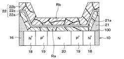
- the upper electrode 22 is configured by laminating a lower metal layer 22a and an upper metal layer 22b from the semiconductor substrate 10 side.
- the lower metal layer 22a of the upper electrode 22 is ohmic-bonded or Schottky-bonded to the semiconductor substrate 10.
- the lower metal layer 22a is ohmic-bonded to the emitter region 18 and the contact region 19, and is Schottky-bonded to the pillar region 20.
- the upper electrode 22 of the present embodiment has an insulating film 22c arranged between the lower metal layer 22a and the upper metal layer 22b.
- the insulating film 22c which will be described in detail later, is a natural oxide film formed by forming a lower metal layer 22a by a sputtering method and then exposing it to the atmosphere, and has an extremely thin thickness of 10 nm or less. There is. Therefore, the lower metal layer 22a and the upper metal layer 22b are electrically connected by the tunnel effect. In FIG. 2, the insulating film 22c is exaggerated to facilitate understanding of the insulating film 22c.
- the upper electrode 22 is in a state in which the particles Ra constituting the lower metal layer 22a and the particles Rb constituting the upper metal layer 22b are separated. That is, the grain boundaries of the particles Ra constituting the lower metal layer 22a and the grain boundaries of the particles Rb constituting the upper metal layer 22b are not connected and are in a separated state. In other words, the grain boundaries of the particles Ra constituting the lower metal layer 22a and the grain boundaries of the particles Rb constituting the upper metal layer 22b are in a state of being terminated in each layer. Therefore, even if nodules are generated in the lower metal layer 22a, the nodules are terminated in the lower metal layer 22a and do not protrude into the upper metal layer 22b.
- nodules may be deposited inside as described above.
- the Schottky barrier may fluctuate due to the stress caused by the nodule, and a leak defect may occur.
- the nodules tend to grow along the thickness direction of the upper electrode 22. That is, the stress caused by the nodules tends to depend on the length of the upper electrode 22 in the nodules along the thickness direction.
- the upper electrode 22 of the present embodiment is in a state in which the nodules in the lower metal layer 22a do not protrude into the upper metal layer 22b as described above. Therefore, the stress caused by the nodules depends on the thickness of the lower metal layer 22a.
- the thickness here is the length along the stacking direction of the lower metal layer 22a and the upper metal layer 22b.
- the present inventors diligently examined the relationship between the thickness of the lower metal layer 22a and the leak defect rate, and obtained the results shown in FIG. As shown in FIG. 3, it is confirmed that the leak defect rate starts to occur when the lower metal layer 22a is 1.5 ⁇ m or more, and sharply increases when the lower metal layer 22a is 2.6 ⁇ m or more. Therefore, in the present embodiment, the thickness of the lower metal layer 22a is set to 2.6 ⁇ m or less. In this case, preferably, the thickness of the lower metal layer 22a is 1.5 ⁇ m or less, so that the leak defect rate can be sufficiently reduced.
- the PN junction formed between the base layer 14 and the drift layer 11 becomes a reverse conduction state and a depletion layer is formed.
- a low level (for example, 0V) voltage lower than the threshold voltage Vth of the insulated gate structure is applied to the gate electrode 17, no current flows between the upper electrode 22 and the lower electrode 26.
- a high level voltage equal to or higher than the threshold voltage Vth of the insulated gate structure is applied to the gate electrode 17 of the IGBT region 1 with a voltage higher than that of the upper electrode 22 applied to the lower electrode 26. Is applied.
- an inversion layer is formed in the portion of the base layer 14 in contact with the trench 15 in which the gate electrode 17 is arranged.
- electrons are supplied from the emitter region 18 to the drift layer 11 via the inversion layer, so that holes are supplied to the drift layer 11 from the collector layer 24, and the resistance value of the drift layer 11 is supplied by conductivity modulation. Turns on when the value drops.
- the IGBT element when the IGBT element is turned off and the FWD element is turned on (that is, the FWD element is operated by a diode), the voltage applied to the upper electrode 22 and the lower electrode 26 is switched, and the lower part is transferred to the upper electrode 22.
- a forward voltage is applied to apply a voltage higher than that of the electrode 26.
- the Schottky junction between the upper electrode 22 and the pillar region 20 is turned on.
- electrons flow from the lower electrode 26 toward the upper electrode 22 via the cathode layer 25, the drift layer 11, the electric field relaxation region 12, the barrier region 13, and the pillar region 20, and the potential of the barrier region 13 is the potential of the upper electrode 22.
- the potential is close to the potential.
- the Schottky junction is turned on first, so that the timing at which the PN junction is turned on is delayed. As a result, the inflow of holes into the drift layer 11 is suppressed. Therefore, when the FWD element recovers, the recovery current can be reduced and the recovery loss can be reduced.
- the parasitic diode is also formed in the IGBT region 1 by the PN junction between the base layer 14 and the barrier region 13.
- the barrier region 13 of the IGBT element in this PN junction is connected to the upper electrode 22 via the pillar region 20. Therefore, as described above, when the potential of the upper electrode 22 rises, a current first flows in the pillar region 20. After that, when the forward voltage rises further, the PN junction constituting the parasitic diode is turned on. As described above, even within the IGBT region 1, the timing at which the PN junction is turned on is delayed, and the inflow of holes into the drift layer 11 is suppressed. This also suppresses the recovery current.
- the electric field relaxation region 12 is formed between the barrier region 13 and the drift layer 11. Therefore, as compared with the case where the electric field relaxation region 12 is not formed, the PN junction formed between the electric field relaxation region 12 and the drift layer 11 makes it difficult for the equipotential lines to enter between the trenches 15. .. Therefore, the withstand voltage can be improved.
- a semiconductor substrate 10 having a base layer 14, an emitter region 18, a contact region 19, a pillar region 20, and the like formed by performing a predetermined semiconductor manufacturing process is prepared.
- the interlayer insulating film 21 is formed on one surface 10a of the semiconductor substrate 10, and the contact hole 21a is formed in the interlayer insulating film 21.
- the semiconductor substrate 10 is arranged in the sputtering apparatus, and the lower metal layer 22a is formed by the sputtering method.
- the lower metal layer 22a is configured by adding an element having a solid solubility limit or higher with respect to the temperature at the time of sputtering so that alloy spikes are less likely to occur. Therefore, it is not necessary to form a barrier metal or the like because alloy spikes are less likely to occur at the portion where the upper electrode 22 is ohmic-bonded to the semiconductor substrate 10.
- the upper electrode 22 having a portion to be ohmic-bonded to the semiconductor substrate 10 and a portion to be Schottky-bonded can be formed in the same process without forming a barrier metal or the like.
- the lower metal layer 22a is formed so as to have a thickness of 2.6 ⁇ m or less as described above.
- the semiconductor substrate 10 is taken out from the sputtering apparatus and exposed to the atmosphere to form the insulating film 22c on the lower metal layer 22a.
- the semiconductor substrate 10 is arranged in the sputtering apparatus again, and the same sputtering method as that for the lower metal layer 22a is performed to form the upper metal layer 22b. As a result, the upper electrode 22 of the present embodiment is formed.
- the grain boundaries of the particles Ra constituting the lower metal layer 22a may protrude into the upper metal layer 22b in the upper metal layer 22b. No. That is, it is suppressed that the nodules generated in the lower metal layer 22a increase in the thickness direction of the upper electrode 22. Therefore, a semiconductor device in which leak defects are unlikely to occur is manufactured.
- the upper electrode 22 is configured by laminating the upper metal layer 22b on the lower metal layer 22a.
- the grain boundaries in the lower metal layer 22a and the grain boundaries in the upper metal layer 22b are not connected and are separated.
- the thickness of the lower metal layer 22a is set to 2.6 ⁇ m or less. Therefore, even if nodules are formed in the portion of the lower metal layer 22a to be Schottky-bonded, it is possible to suppress an increase in the leak defect rate.
- the thickness of the lower metal layer 22a is set to 1.5 ⁇ m or less. Therefore, even if the size of the semiconductor substrate 10 is increased in the plane direction, it is possible to suppress an increase in the leak defect rate, and it is possible to improve the degree of freedom in designing the semiconductor device.
- the lower metal layer 22a when the lower metal layer 22a is formed, an element having a solid solution solubility or higher at the temperature at the time of sputtering is added. Therefore, it is possible to suppress the occurrence of alloy spikes, and the lower metal layer 22a can be ohmic-bonded to the semiconductor substrate 10 without forming a barrier metal. That is, the lower metal layer 22a having the ohmic-bonded portion and the Schottky-bonded portion can be formed in the same process without forming the barrier metal.
- the lower metal layer 22a is formed by adding an element having a solid solubility limit or higher at the temperature at the time of sputtering, nodules are likely to be generated, but the thickness of the lower metal layer 22a is 2.6 ⁇ m or less. , The increase in leak defect rate is suppressed.
- the average particle size of the particles Rb constituting the upper metal layer 22b is smaller than the average particle size of the particles Ra constituting the lower metal layer 22a as compared with the first embodiment.
- Others are the same as those in the first embodiment, and thus description thereof will be omitted here.
- the average particle size of the particles Rb constituting the upper metal layer 22b is made smaller than the average particle size of the particles Ra constituting the lower metal layer 22a. It is said that it has a structure.
- Such an upper electrode 22 is manufactured as follows.
- the sputtering method is performed at a high temperature of 400 ° C. or higher.
- the sputtering method is performed at a temperature lower than the sputtering method for forming the lower metal layer 22a.
- a sputtering method is performed at about 300 to 350 ° C.
- the average particle size of the particles Rb constituting the upper metal layer 22b is the particles constituting the lower metal layer 22a. It is smaller than the average particle size of Ra.
- the average particle size of the particles Rb constituting the upper metal layer 22b is smaller than the average particle size of the particles Ra constituting the lower metal layer 22a. Therefore, as compared with the case where the average particle size of the particles Rb constituting the upper metal layer 22b is equal to or larger than the average particle size of the particles Ra constituting the lower metal layer 22a, the lower metal layer 22a in the upper metal layer 22b On the surface opposite to the side, the grain boundary step becomes small. Therefore, when performing a visual inspection, it is possible to reduce the possibility that the grain boundary step is erroneously determined as a defect or a foreign substance.
- the third embodiment will be described.
- the insulating film 22c is not arranged between the upper metal layer 22b and the lower metal layer 22a as compared with the first embodiment. Others are the same as those in the first embodiment, and thus description thereof will be omitted here.
- the upper electrode 22 has a configuration in which the insulating film 22c is not arranged between the lower metal layer 22a and the upper metal layer 22b.
- Such an upper electrode 22 is manufactured as follows.
- an inert gas such as argon is introduced into the sputtering apparatus, and the lower metal layer 22a is cooled to form the lower metal layer 22a.
- the growth of the particle Ra is completely stopped.
- the process of FIG. 4C is performed without performing the process of FIG. 4B.
- the upper metal layer 22b is composed of particles Rb different from the particles Ra constituting the lower metal layer 22a. Therefore, the particles Ra constituting the lower metal layer 22a and the particles Rb constituting the upper metal layer 22b are separated from each other.
- the particles Ra constituting the lower metal layer 22a and the particles Rb constituting the upper metal layer 22b are formed. If it is in a divided state, the same effect as that of the first embodiment can be obtained.
- the semiconductor device has the IGBT region 1 and the FWD region 2, but if the semiconductor device has a Schottky-bonded portion, it has only one of the IGBT region 1 and the FWD region 2. It may be configured. Further, the upper electrode 22 may be configured to have only a portion to be Schottky-bonded, or may not have a portion to be ohmic-bonded. Further, in each of the above embodiments, the composition of the lower metal layer 22a and the composition of the upper metal layer 22b may be different.
- each of the above embodiments can be combined.
- the second embodiment is combined with the third embodiment so that the average particle size of the particles Rb constituting the upper metal layer 22b is smaller than the average particle size of the particles Ra constituting the lower metal layer 22a. May be good.
- a combination of the above embodiments may be combined.
Abstract
In the present invention, the following are provided: a semiconductor substrate (10); and a metal film (22) that is formed on top of the semiconductor substrate (10), that has a section which forms a Schottky junction with the semiconductor substrate (10), and that is made of an aluminum alloy in which an element is added to aluminum. The metal film (22) is constituted by stacking a lower metal layer (22a) disposed on the side of the semiconductor substrate (10) and an upper metal layer (22b) that is disposed on top of the lower metal layer (22a). Furthermore, the lower metal layer (22a) is set to have a thickness of 2.6 μm or less along the stacking direction of the lower metal layer (22a) and the upper metal layer (22b).
Description
本出願は、2020年6月26日に出願された日本特許出願番号2020-110888号に基づくもので、ここにその記載内容が参照により組み入れられる。
This application is based on Japanese Patent Application No. 2020-110888 filed on June 26, 2020, the contents of which are incorporated herein by reference.
本開示は、ショットキー接合を有する半導体装置およびその製造方法に関する。
The present disclosure relates to a semiconductor device having a Schottky junction and a method for manufacturing the same.
従来より、シリコン等の半導体基板上にショットキー接合される金属膜が配置された半導体装置が提案されている。なお、金属膜は、アルミニウムにシリコンや銅等の元素が添加されたアルミニウム合金で構成される。このような半導体装置では、金属膜内にノジュールが形成されると、ショットキー接合される部分にノジュールに起因した応力が印加されることがある。そして、応力が大きい場合には、ショットキー障壁が変化する可能性があり、リーク不良率が高くなる可能性がある。
このため、例えば、特許文献1には、ショットキー接合される部分を規定した半導体装置が提案されている。具体的には、この半導体装置は、半導体基板上に層間絶縁膜が形成され、層間絶縁膜に半導体基板を露出させるコンタクトホールが形成されている。また、半導体装置は、金属膜がコンタクトホールを通じて半導体基板とショットキー接合される部分を含むように形成されている。そして、この半導体装置は、金属膜に形成されるノジュールが層間絶縁膜の開口部近傍に形成され易いため、ショットキー接合される部分が層間絶縁膜の開口部近傍から離れた位置となるようにしている。詳しくは、半導体装置は、半導体基板のうちの層間絶縁膜から露出する部分において、開口部近傍側では金属膜が半導体基板とオーミック接合され、内縁部側において金属膜が半導体基板とショットキー接合されるように構成されている。 Conventionally, a semiconductor device in which a metal film to be Schottky-bonded is arranged on a semiconductor substrate such as silicon has been proposed. The metal film is composed of an aluminum alloy in which elements such as silicon and copper are added to aluminum. In such a semiconductor device, when nodules are formed in the metal film, stress due to the nodules may be applied to the portion to be Schottky-bonded. And when the stress is large, the Schottky barrier may change and the leak defect rate may increase.
Therefore, for example,Patent Document 1 proposes a semiconductor device that defines a portion to be Schottky-bonded. Specifically, in this semiconductor device, an interlayer insulating film is formed on the semiconductor substrate, and a contact hole for exposing the semiconductor substrate is formed in the interlayer insulating film. Further, the semiconductor device is formed so as to include a portion where the metal film is Schottky-bonded to the semiconductor substrate through the contact hole. In this semiconductor device, nodules formed on the metal film are likely to be formed near the opening of the interlayer insulating film, so that the portion to be Schottky-bonded is located away from the vicinity of the opening of the interlayer insulating film. ing. Specifically, in the semiconductor device, in the portion of the semiconductor substrate exposed from the interlayer insulating film, the metal film is ohmic-bonded to the semiconductor substrate on the side near the opening, and the metal film is Schottky-bonded to the semiconductor substrate on the inner edge side. It is configured to be.
このため、例えば、特許文献1には、ショットキー接合される部分を規定した半導体装置が提案されている。具体的には、この半導体装置は、半導体基板上に層間絶縁膜が形成され、層間絶縁膜に半導体基板を露出させるコンタクトホールが形成されている。また、半導体装置は、金属膜がコンタクトホールを通じて半導体基板とショットキー接合される部分を含むように形成されている。そして、この半導体装置は、金属膜に形成されるノジュールが層間絶縁膜の開口部近傍に形成され易いため、ショットキー接合される部分が層間絶縁膜の開口部近傍から離れた位置となるようにしている。詳しくは、半導体装置は、半導体基板のうちの層間絶縁膜から露出する部分において、開口部近傍側では金属膜が半導体基板とオーミック接合され、内縁部側において金属膜が半導体基板とショットキー接合されるように構成されている。 Conventionally, a semiconductor device in which a metal film to be Schottky-bonded is arranged on a semiconductor substrate such as silicon has been proposed. The metal film is composed of an aluminum alloy in which elements such as silicon and copper are added to aluminum. In such a semiconductor device, when nodules are formed in the metal film, stress due to the nodules may be applied to the portion to be Schottky-bonded. And when the stress is large, the Schottky barrier may change and the leak defect rate may increase.
Therefore, for example,
しかしながら、上記半導体装置では、ノジュールが形成され易い部分と異なる部分でショットキー接合が構成されるようにしているが、開口部近傍から離れた位置にもノジュールが形成される可能性がある。そして、例えば、半導体基板を面方向に大型化する場合等には、ノジュールの影響を無視できなくなる可能性があり、リーク不良率が高くなる可能性がある。
However, in the above semiconductor device, although the Schottky junction is formed in a portion different from the portion where nodules are easily formed, there is a possibility that nodules are also formed at a position away from the vicinity of the opening. Then, for example, when the size of the semiconductor substrate is increased in the plane direction, the influence of nodules may not be negligible, and the leak defect rate may increase.
本開示は、リーク不良率が高くなることを抑制できる半導体装置およびその製造方法を提供することを目的とする。
An object of the present disclosure is to provide a semiconductor device capable of suppressing an increase in the leak defect rate and a method for manufacturing the same.
本開示の1つの観点によれば、半導体装置は、半導体基板と、半導体基板上に形成され、半導体基板とショットキー接合される部分を有し、アルミニウムに元素が添加されたアルミニウム合金で構成された金属膜と、を備え、金属膜は、半導体基板側に配置される下層金属層と、下層金属層上に配置される上層金属層とが積層されて構成されており、下層金属層は、下層金属層と上層金属層との積層方向に沿った厚さが2.6μm以下とされている。
According to one aspect of the present disclosure, the semiconductor device is composed of a semiconductor substrate, a portion formed on the semiconductor substrate and bonded to the semiconductor substrate by shot key, and an aluminum alloy in which an element is added to aluminum. The metal film is configured by laminating a lower metal layer arranged on the semiconductor substrate side and an upper metal layer arranged on the lower metal layer. The thickness of the lower metal layer and the upper metal layer along the stacking direction is 2.6 μm or less.
これによれば、下層金属層の厚さが2.6μm以下とされているため、リーク不良率が高くなることを抑制できる。
According to this, since the thickness of the lower metal layer is 2.6 μm or less, it is possible to suppress an increase in the leak defect rate.
本開示の別の観点によれば、半導体装置の製造方法は、半導体基板を用意することと、半導体基板上に、半導体基板とショットキー接合される部分を有し、金属膜のうちの半導体基板側に配置される下層金属層を形成することと、下層金属層上に上層金属層を形成することと、を行うことにより、下層金属層および上層金属層を有する金属膜を形成することと、を行い、下層金属層を形成することでは、下層金属層と上層金属層との積層方向に沿った厚さが2.6μm以下となる下層金属層を形成する。
According to another aspect of the present disclosure, a method for manufacturing a semiconductor device includes preparing a semiconductor substrate and having a portion on the semiconductor substrate that is Schottky-bonded to the semiconductor substrate, and the semiconductor substrate among the metal films. By forming the lower metal layer arranged on the side and forming the upper metal layer on the lower metal layer, a metal film having the lower metal layer and the upper metal layer is formed. By forming the lower metal layer, a lower metal layer having a thickness of 2.6 μm or less along the stacking direction of the lower metal layer and the upper metal layer is formed.
これによれば、厚さが2.6μm以下となるように下層金属層を形成するため、リーク不良率が高くなることを抑制した半導体装置を製造できる。
According to this, since the lower metal layer is formed so that the thickness is 2.6 μm or less, it is possible to manufacture a semiconductor device in which the leakage defect rate is suppressed from increasing.
なお、各構成要素等に付された括弧付きの参照符号は、その構成要素等と後述する実施形態に記載の具体的な構成要素等との対応関係の一例を示すものである。
The reference numerals in parentheses attached to each component or the like indicate an example of the correspondence between the component or the like and the specific component or the like described in the embodiment described later.
以下、本開示の実施形態について図に基づいて説明する。なお、以下の各実施形態相互において、互いに同一もしくは均等である部分には、同一符号を付して説明を行う。
Hereinafter, embodiments of the present disclosure will be described with reference to the figures. In each of the following embodiments, the parts that are the same or equal to each other will be described with the same reference numerals.
(第1実施形態)
第1実施形態について、図面を参照しつつ説明する。図1に示されるように、半導体装置は、IGBT(Insulated Gate Bipolar Transistorの略)素子を有するIGBT領域1と、FWD素子(Free Wheeling Diodeの略)を有するFWD領域2とが共通の半導体基板10に形成されて構成されている。つまり、本実施形態の半導体装置は、RC(Reverse Conductingの略)-IGBTとされている。なお、具体的には後述するが、本実施形態の半導体装置は、半導体基板10の他面10bに位置するコレクタ層24上の部分がIGBT領域1とされ、半導体基板10の他面10bに位置するカソード層25上の部分がFWD領域2とされている。 (First Embodiment)
The first embodiment will be described with reference to the drawings. As shown in FIG. 1, the semiconductor device has asemiconductor substrate 10 in which an IGBT region 1 having an IGBT (abbreviation for Insulated Gate Bipolar Transistor) element and an FWD region 2 having an FWD element (abbreviation for Free Wheeling Diode) are common. It is formed and configured in. That is, the semiconductor device of this embodiment is RC (abbreviation of Reverse Conducting) -IGBT. As will be described specifically later, in the semiconductor device of the present embodiment, the portion on the collector layer 24 located on the other surface 10b of the semiconductor substrate 10 is defined as the IGBT region 1, and is located on the other surface 10b of the semiconductor substrate 10. The portion on the cathode layer 25 is the FWD region 2.
第1実施形態について、図面を参照しつつ説明する。図1に示されるように、半導体装置は、IGBT(Insulated Gate Bipolar Transistorの略)素子を有するIGBT領域1と、FWD素子(Free Wheeling Diodeの略)を有するFWD領域2とが共通の半導体基板10に形成されて構成されている。つまり、本実施形態の半導体装置は、RC(Reverse Conductingの略)-IGBTとされている。なお、具体的には後述するが、本実施形態の半導体装置は、半導体基板10の他面10bに位置するコレクタ層24上の部分がIGBT領域1とされ、半導体基板10の他面10bに位置するカソード層25上の部分がFWD領域2とされている。 (First Embodiment)
The first embodiment will be described with reference to the drawings. As shown in FIG. 1, the semiconductor device has a
半導体装置は、N-型のドリフト層11を構成する半導体基板10を有している。なお、本実施形態では、半導体基板10は、シリコン基板で構成される。そして、ドリフト層11上には、ドリフト層11より低不純物濃度とされたP-型の電界緩和領域12、ドリフト層11より高不純物濃度とされたN型のバリア領域13がドリフト層11側から順に形成されている。バリア領域13上には、電界緩和領域12より高不純物濃度とされたP型のベース層14が形成されている。なお、ドリフト層11上とは、言い換えると半導体基板10の一面10a側のことである。
The semiconductor device has a semiconductor substrate 10 constituting an N-type drift layer 11. In this embodiment, the semiconductor substrate 10 is composed of a silicon substrate. Then, on the drift layer 11, a P - type electric field relaxation region 12 having a lower impurity concentration than the drift layer 11 and an N-type barrier region 13 having a higher impurity concentration than the drift layer 11 are formed from the drift layer 11 side. It is formed in order. A P-type base layer 14 having a higher impurity concentration than the electric field relaxation region 12 is formed on the barrier region 13. In other words, the top of the drift layer 11 is one side 10a of the semiconductor substrate 10.
半導体基板10には、一面10a側からベース層14、バリア領域13、および電界緩和領域12を貫通してドリフト層11に達するように複数のトレンチ15が形成されている。これにより、ベース層14、バリア領域13、および電界緩和領域12は、トレンチ15によって複数個に分離されている。本実施形態では、複数のトレンチ15は、IGBT領域1およびFWD領域2にそれぞれ形成されている。また、本実施形態では、複数のトレンチ15は、IGBT領域1およびFWD領域2の配列方向と交差する一方向を長手方向(すなわち、図1中の紙面奥行き方向)としてストライプ状に形成されている。
A plurality of trenches 15 are formed on the semiconductor substrate 10 so as to pass through the base layer 14, the barrier region 13, and the electric field relaxation region 12 from the one surface 10a side to reach the drift layer 11. As a result, the base layer 14, the barrier region 13, and the electric field relaxation region 12 are separated into a plurality of parts by the trench 15. In the present embodiment, the plurality of trenches 15 are formed in the IGBT region 1 and the FWD region 2, respectively. Further, in the present embodiment, the plurality of trenches 15 are formed in a striped shape with one direction intersecting the arrangement direction of the IGBT region 1 and the FWD region 2 as the longitudinal direction (that is, the depth direction of the paper surface in FIG. 1). ..
各トレンチ15は、各トレンチ15の壁面を覆うように形成されたゲート絶縁膜16と、このゲート絶縁膜16の上に形成されたポリシリコン等により構成されるゲート電極17とにより埋め込まれている。これにより、トレンチゲート構造が構成されている。
Each trench 15 is embedded by a gate insulating film 16 formed so as to cover the wall surface of each trench 15 and a gate electrode 17 formed of polysilicon or the like formed on the gate insulating film 16. .. This constitutes a trench gate structure.
なお、特に図示しないが、IGBT領域1に形成されたゲート電極17は、図示しないゲートパッド等を介してゲートドライバ等に接続され、所定の電圧が印加されるようになっている。また、FWD領域2に形成されたゲート電極17は、所定電位に維持されるようになっている。例えば、FWD領域2に形成されたゲート電極17は、後述する上部電極22と接続され、上部電極22と同電位とされる。
Although not shown in particular, the gate electrode 17 formed in the IGBT region 1 is connected to a gate driver or the like via a gate pad or the like (not shown), and a predetermined voltage is applied. Further, the gate electrode 17 formed in the FWD region 2 is maintained at a predetermined potential. For example, the gate electrode 17 formed in the FWD region 2 is connected to the upper electrode 22 described later and has the same potential as the upper electrode 22.
ベース層14には、エミッタ領域18、コンタクト領域19、ピラー領域20が形成されている。エミッタ領域18は、ドリフト層11よりも高不純物濃度とされたN+型とされ、ベース層14層の表層部に形成されている。具体的には、エミッタ領域18は、ベース層14内において終端し、かつ、トレンチ15の側面に接するように形成されている。より詳しくは、エミッタ領域18は、隣合うトレンチ15間の領域において、トレンチ15の長手方向に沿ってトレンチ15の側面に接するように棒状に延設され、トレンチ15の先端よりも内側で終端する構造とされている。
The base layer 14 is formed with an emitter region 18, a contact region 19, and a pillar region 20. The emitter region 18 has an N + type having a higher impurity concentration than the drift layer 11, and is formed on the surface layer of the base layer 14. Specifically, the emitter region 18 is formed so as to be terminated in the base layer 14 and to be in contact with the side surface of the trench 15. More specifically, the emitter region 18 extends in a rod shape along the longitudinal direction of the trench 15 so as to be in contact with the side surface of the trench 15 in the region between the adjacent trenches 15, and terminates inside the tip of the trench 15. It is said to be a structure.
コンタクト領域19は、ベース層14よりも高不純物濃度とされたP+型とされ、ベース層14の表層部に形成されている。具体的には、コンタクト領域19は、ベース層14内において終端し、かつ2つのエミッタ領域18に挟まれるように形成されている。より詳しくは、コンタクト領域19は、エミッタ領域18と接するように、トレンチ15の長手方向に沿って棒状に延設されている。
The contact region 19 is a P + type having a higher impurity concentration than the base layer 14, and is formed on the surface layer portion of the base layer 14. Specifically, the contact region 19 is formed so as to be terminated in the base layer 14 and sandwiched between the two emitter regions 18. More specifically, the contact region 19 extends in a rod shape along the longitudinal direction of the trench 15 so as to be in contact with the emitter region 18.
ピラー領域20は、バリア領域13と同程度の不純物濃度とされており、コンタクト領域19およびベース層14を貫通してバリア領域13に達するように形成されている。つまり、ピラー領域20は、バリア領域13と接続されるように形成されている。
The pillar region 20 has an impurity concentration similar to that of the barrier region 13, and is formed so as to penetrate the contact region 19 and the base layer 14 and reach the barrier region 13. That is, the pillar region 20 is formed so as to be connected to the barrier region 13.
半導体基板10の一面10a上には、BPSG(Borophosphosilicate Glassの略)等で構成される層間絶縁膜21が形成されている。層間絶縁膜21には、エミッタ領域18、コンタクト領域19、ピラー領域20を露出させるコンタクトホール21aが形成されている。
An interlayer insulating film 21 made of BPSG (abbreviation of Borophosphosilicate Glass) or the like is formed on one surface 10a of the semiconductor substrate 10. The interlayer insulating film 21 is formed with a contact hole 21a that exposes the emitter region 18, the contact region 19, and the pillar region 20.
そして、層間絶縁膜21上には、金属膜に相当する上部電極22が形成されている。上部電極22は、IGBT領域1およびFWD領域2において、層間絶縁膜21に形成されたコンタクトホール21aを通じ、エミッタ領域18およびコンタクト領域19とオーミック接合されていると共に、ピラー領域20とショットキー接合されている。つまり、本実施形態の上部電極22は、ショットキー接合される部分とオーミック接合される部分とを共に含む構成とされている。そして、このように上部電極22が形成されていることにより、上部電極22は、IGBT領域1においてエミッタ電極として機能し、FWD領域2においてアノード電極として機能する。なお、上部電極22の具体的な構成については後述する。
An upper electrode 22 corresponding to a metal film is formed on the interlayer insulating film 21. The upper electrode 22 is ohmic-bonded to the emitter region 18 and the contact region 19 and Schottky-bonded to the pillar region 20 through the contact hole 21a formed in the interlayer insulating film 21 in the IGBT region 1 and the FWD region 2. ing. That is, the upper electrode 22 of the present embodiment is configured to include both a Schottky-bonded portion and an ohmic-bonded portion. Since the upper electrode 22 is formed in this way, the upper electrode 22 functions as an emitter electrode in the IGBT region 1 and as an anode electrode in the FWD region 2. The specific configuration of the upper electrode 22 will be described later.
ドリフト層11のうちのベース層14側と反対側には、ドリフト層11よりも高キャリア濃度とされたN型のフィールドストップ層(以下では、FS層という)23が形成されている。つまり、半導体基板10の他面10b側には、FS層23が形成されている。
An N-type field stop layer (hereinafter referred to as an FS layer) 23 having a higher carrier concentration than the drift layer 11 is formed on the side of the drift layer 11 opposite to the base layer 14 side. That is, the FS layer 23 is formed on the other surface 10b side of the semiconductor substrate 10.
IGBT領域1では、FS層23を挟んでドリフト層11と反対側にP+型のコレクタ層24が形成され、FWD領域2では、FS層23を挟んでドリフト層11と反対側にN+型のカソード層25が形成されている。そして、本実施形態では、IGBT領域1とFWD領域2とは、半導体基板10の他面10bに位置する層がコレクタ層24であるかカソード層25であるかによって区画されている。つまり、本実施形態の半導体装置では、コレクタ層24上の部分がIGBT領域1とされ、カソード層25上の部分がFWD領域2とされている。
In the IGBT region 1, a P + type collector layer 24 is formed on the side opposite to the drift layer 11 with the FS layer 23 interposed therebetween, and in the FWD region 2, an N + type collector layer 24 is formed on the opposite side of the drift layer 11 with the FS layer 23 interposed therebetween. The cathode layer 25 is formed. In the present embodiment, the IGBT region 1 and the FWD region 2 are partitioned by whether the layer located on the other surface 10b of the semiconductor substrate 10 is the collector layer 24 or the cathode layer 25. That is, in the semiconductor device of the present embodiment, the portion on the collector layer 24 is the IGBT region 1, and the portion on the cathode layer 25 is the FWD region 2.
コレクタ層24およびカソード層25を挟んでドリフト層11と反対側には、コレクタ層24およびカソード層25と電気的に接続される下部電極26が形成されている。言い換えると、半導体基板10の他面10bには、IGBT領域1においてはコレクタ電極として機能し、FWD領域2においてはカソード電極として機能する下部電極26が形成されている。
A lower electrode 26 electrically connected to the collector layer 24 and the cathode layer 25 is formed on the side opposite to the drift layer 11 with the collector layer 24 and the cathode layer 25 interposed therebetween. In other words, a lower electrode 26 that functions as a collector electrode in the IGBT region 1 and a cathode electrode in the FWD region 2 is formed on the other surface 10b of the semiconductor substrate 10.
本実施形態の半導体装置は、このように構成されることにより、IGBT領域1においては、ベース層14をベースとし、エミッタ領域18をエミッタとし、コレクタ層24をコレクタとするIGBT素子が構成される。また、FWD領域2においては、ベース層をアノードとし、ドリフト層11、FS層23、カソード層25をカソードとしてPN接合されたFWD素子が構成される。
By being configured in this way, the semiconductor device of the present embodiment comprises an IGBT element having a base layer 14 as a base, an emitter region 18 as an emitter, and a collector layer 24 as a collector in the IGBT region 1. .. Further, in the FWD region 2, a PN-junctioned FWD element is configured with the base layer as an anode and the drift layer 11, the FS layer 23, and the cathode layer 25 as cathodes.
以上が本実施形態における半導体装置の基本的な構成である。なお、本実施形態では、N型、N+型、N-型が第1導電型に相当しており、P型、P-型、P+型が第2導電型に相当している。また、本実施形態では、上記のように構成されることにより、半導体基板10は、コレクタ層24、カソード層25、FS層23、ドリフト層11、電界緩和領域12、バリア領域13、ベース層14、エミッタ領域18、コンタクト領域19、ピラー領域20を含んだ構成となっている。
The above is the basic configuration of the semiconductor device in this embodiment. In this embodiment, N-type, N + -type, and N - type correspond to the first conductive type, and P-type, P - type, and P + type correspond to the second conductive type. Further, in the present embodiment, the semiconductor substrate 10 is configured as described above, so that the semiconductor substrate 10 has a collector layer 24, a cathode layer 25, an FS layer 23, a drift layer 11, an electric field relaxation region 12, a barrier region 13, and a base layer 14. , The emitter region 18, the contact region 19, and the pillar region 20 are included.
次に、本実施形態の上部電極22について具体的に説明する。本実施形態の上部電極22は、アルミニウムに元素が添加されたアルミニウム合金で構成されており、例えば、AlSi、AlCu、AlSiCu等で構成されている。また、本実施形態では、上部電極22は、後述するようにスパッタ法によって形成されるが、アロイスパイクが発生し難くなるように、添加される元素がスパッタ時の温度に対する限界固溶度以上に添加されている。そして、本実施形態の上部電極22は、半導体装置の特性検査を行うためのプローブ針等が当接された際、破壊され難いように厚さが3μm以上の厚膜とされている。
Next, the upper electrode 22 of the present embodiment will be specifically described. The upper electrode 22 of the present embodiment is made of an aluminum alloy in which an element is added to aluminum, and is made of, for example, AlSi, AlCu, AlSiCu, or the like. Further, in the present embodiment, the upper electrode 22 is formed by a sputtering method as described later, but the added element has a solid solution solubility or higher with respect to the temperature at the time of sputtering so that alloy spikes are less likely to occur. Has been added. The upper electrode 22 of the present embodiment is made of a thick film having a thickness of 3 μm or more so as not to be easily broken when a probe needle or the like for inspecting the characteristics of the semiconductor device is brought into contact with the upper electrode 22.
上部電極22は、図2に示されるように、半導体基板10側から下層金属層22aおよび上層金属層22bが積層されて構成されている。そして、上部電極22は、下層金属層22aが半導体基板10とオーミック接合、またはショットキー接合されている。具体的には、上部電極22は、下層金属層22aがエミッタ領域18およびコンタクト領域19とオーミック接合されていると共に、ピラー領域20とショットキー接合されている。
As shown in FIG. 2, the upper electrode 22 is configured by laminating a lower metal layer 22a and an upper metal layer 22b from the semiconductor substrate 10 side. The lower metal layer 22a of the upper electrode 22 is ohmic-bonded or Schottky-bonded to the semiconductor substrate 10. Specifically, in the upper electrode 22, the lower metal layer 22a is ohmic-bonded to the emitter region 18 and the contact region 19, and is Schottky-bonded to the pillar region 20.
また、本実施形態の上部電極22は、下層金属層22aと上層金属層22bとの間に配置される絶縁膜22cを有している。この絶縁膜22cは、具体的には後述するが、スパッタ法で下層金属層22aを成膜した後に大気に晒すことで構成される自然酸化膜であり、厚さが極めて薄い10nm以下とされている。このため、下層金属層22aと上層金属層22bとは、トンネル効果によって電気的に接続されている。なお、図2では、絶縁膜22cの理解をし易くするため、絶縁膜22cを誇張して示してある。
Further, the upper electrode 22 of the present embodiment has an insulating film 22c arranged between the lower metal layer 22a and the upper metal layer 22b. The insulating film 22c, which will be described in detail later, is a natural oxide film formed by forming a lower metal layer 22a by a sputtering method and then exposing it to the atmosphere, and has an extremely thin thickness of 10 nm or less. There is. Therefore, the lower metal layer 22a and the upper metal layer 22b are electrically connected by the tunnel effect. In FIG. 2, the insulating film 22c is exaggerated to facilitate understanding of the insulating film 22c.
そして、上部電極22は、下層金属層22aを構成する粒子Raと上層金属層22bを構成する粒子Rbとが分断された状態となっている。つまり、下層金属層22aを構成する粒子Raの粒界と、上層金属層22bを構成する粒子Rbの粒界とは、繋がっておらず、分断された状態となっている。言い換えると、下層金属層22aを構成する粒子Raの粒界、および上層金属層22bを構成する粒子Rbの粒界は、それぞれ各層内で終端した状態となっている。このため、下層金属層22a内にノジュールが発生したとしても、ノジュールは、当該下層金属層22a内で終端し、上層金属層22bに突き出さない状態となる。
The upper electrode 22 is in a state in which the particles Ra constituting the lower metal layer 22a and the particles Rb constituting the upper metal layer 22b are separated. That is, the grain boundaries of the particles Ra constituting the lower metal layer 22a and the grain boundaries of the particles Rb constituting the upper metal layer 22b are not connected and are in a separated state. In other words, the grain boundaries of the particles Ra constituting the lower metal layer 22a and the grain boundaries of the particles Rb constituting the upper metal layer 22b are in a state of being terminated in each layer. Therefore, even if nodules are generated in the lower metal layer 22a, the nodules are terminated in the lower metal layer 22a and do not protrude into the upper metal layer 22b.
ここで、上部電極22を構成するアルミニウム合金は、上記のように、内部にノジュールが析出することがある。そして、ノジュールがショットキー接合される部分に構成されると、ノジュールに起因する応力によってショットキー障壁が変動する可能性があり、リーク不良が発生する可能性がある。この場合、ノジュールは、上部電極22の厚さ方向に沿って成長し易い。つまり、ノジュールに起因する応力は、ノジュールにおける上部電極22の厚さ方向に沿った長さに依存し易い。
Here, in the aluminum alloy constituting the upper electrode 22, nodules may be deposited inside as described above. When the nodule is formed in the portion to be Schottky-joined, the Schottky barrier may fluctuate due to the stress caused by the nodule, and a leak defect may occur. In this case, the nodules tend to grow along the thickness direction of the upper electrode 22. That is, the stress caused by the nodules tends to depend on the length of the upper electrode 22 in the nodules along the thickness direction.
そして、本実施形態の上部電極22は、上記のように下層金属層22a内のノジュールが上層金属層22b内に突き出さない状態となっている。このため、ノジュールに起因する応力は、下層金属層22aの厚さに依存する。なお、ここでの厚さとは、下層金属層22aと上層金属層22bとの積層方向に沿った長さのことである。
The upper electrode 22 of the present embodiment is in a state in which the nodules in the lower metal layer 22a do not protrude into the upper metal layer 22b as described above. Therefore, the stress caused by the nodules depends on the thickness of the lower metal layer 22a. The thickness here is the length along the stacking direction of the lower metal layer 22a and the upper metal layer 22b.
そして、本発明者らは、下層金属層22aの厚さと、リーク不良率との関係について鋭意検討を行い、図3に示される結果を得た。図3に示されるように、リーク不良率は、下層金属層22aが1.5μm以上になると発生し始め、下層金属層22aが2.6μm以上になると急峻に大きくなることが確認される。したがって、本実施形態では、下層金属層22aの厚さが2.6μm以下とされている。この場合、好ましくは、下層金属層22aの厚さが1.5μm以下とされることにより、リーク不良率を十分に低減できる。
Then, the present inventors diligently examined the relationship between the thickness of the lower metal layer 22a and the leak defect rate, and obtained the results shown in FIG. As shown in FIG. 3, it is confirmed that the leak defect rate starts to occur when the lower metal layer 22a is 1.5 μm or more, and sharply increases when the lower metal layer 22a is 2.6 μm or more. Therefore, in the present embodiment, the thickness of the lower metal layer 22a is set to 2.6 μm or less. In this case, preferably, the thickness of the lower metal layer 22a is 1.5 μm or less, so that the leak defect rate can be sufficiently reduced.
以上が本実施形態における半導体装置の構成である。次に、上記半導体装置の基本的な作動について説明する。
The above is the configuration of the semiconductor device in this embodiment. Next, the basic operation of the semiconductor device will be described.
半導体装置は、下部電極26に上部電極22より高い電圧が印加されると、ベース層14とドリフト層11との間に形成されるPN接合が逆導通状態となって空乏層が形成される。そして、ゲート電極17に、絶縁ゲート構造の閾値電圧Vth未満であるローレベル(例えば、0V)の電圧が印加されているときには、上部電極22と下部電極26との間に電流は流れない。
In the semiconductor device, when a voltage higher than that of the upper electrode 22 is applied to the lower electrode 26, the PN junction formed between the base layer 14 and the drift layer 11 becomes a reverse conduction state and a depletion layer is formed. When a low level (for example, 0V) voltage lower than the threshold voltage Vth of the insulated gate structure is applied to the gate electrode 17, no current flows between the upper electrode 22 and the lower electrode 26.
IGBT素子をオン状態にするには、下部電極26に上部電極22より高い電圧が印加された状態で、IGBT領域1のゲート電極17に、絶縁ゲート構造の閾値電圧Vth以上であるハイレベルの電圧が印加されるようにする。これにより、IGBT領域1では、ベース層14のうちのゲート電極17が配置されるトレンチ15と接している部分に反転層が形成される。そして、IGBT素子は、エミッタ領域18から反転層を介して電子がドリフト層11に供給されることによってコレクタ層24から正孔がドリフト層11に供給され、伝導度変調によりドリフト層11の抵抗値が低下することでオン状態となる。
In order to turn on the IGBT element, a high level voltage equal to or higher than the threshold voltage Vth of the insulated gate structure is applied to the gate electrode 17 of the IGBT region 1 with a voltage higher than that of the upper electrode 22 applied to the lower electrode 26. Is applied. As a result, in the IGBT region 1, an inversion layer is formed in the portion of the base layer 14 in contact with the trench 15 in which the gate electrode 17 is arranged. Then, in the IGBT element, electrons are supplied from the emitter region 18 to the drift layer 11 via the inversion layer, so that holes are supplied to the drift layer 11 from the collector layer 24, and the resistance value of the drift layer 11 is supplied by conductivity modulation. Turns on when the value drops.
また、IGBT素子をオフ状態にし、FWD素子をオン状態にする(すなわち、FWD素子をダイオード動作させる)際には、上部電極22と下部電極26に印加する電圧をスイッチングし、上部電極22に下部電極26より高い電圧を印加する順電圧印加を行う。これにより、FWD領域2では、上部電極22とピラー領域20との間のショットキー接合がオンする。そして、下部電極26から、カソード層25、ドリフト層11、電界緩和領域12、バリア領域13、ピラー領域20を介して上部電極22に向かって電子が流れ、バリア領域13の電位が上部電極22の電位に近い電位となる。
Further, when the IGBT element is turned off and the FWD element is turned on (that is, the FWD element is operated by a diode), the voltage applied to the upper electrode 22 and the lower electrode 26 is switched, and the lower part is transferred to the upper electrode 22. A forward voltage is applied to apply a voltage higher than that of the electrode 26. As a result, in the FWD region 2, the Schottky junction between the upper electrode 22 and the pillar region 20 is turned on. Then, electrons flow from the lower electrode 26 toward the upper electrode 22 via the cathode layer 25, the drift layer 11, the electric field relaxation region 12, the barrier region 13, and the pillar region 20, and the potential of the barrier region 13 is the potential of the upper electrode 22. The potential is close to the potential.
このため、FWD領域2では、ベース層14とバリア領域13の境界のPN接合に電位差が生じ難くなる。したがって、その後に上部電極22の電位を上昇させても、しばらくの間は、当該PN接合がオンしない。そして、上部電極22の電位をさらに上昇させると、ショットキー接合を介して流れる電流が増加する。これにより、上部電極22とバリア領域13との間の電位差が大きくなり、PN接合に生じる電位差も大きくなる。したがって、上部電極22の電位を所定の電位以上に上昇させると、PN接合(すなわち、FWD素子)がオンする。そして、バリア領域13とベース層14を介して下部電極26から上部電極22へ向かって電子が流れる。
Therefore, in the FWD region 2, a potential difference is unlikely to occur at the PN junction at the boundary between the base layer 14 and the barrier region 13. Therefore, even if the potential of the upper electrode 22 is subsequently increased, the PN junction does not turn on for a while. Then, when the potential of the upper electrode 22 is further increased, the current flowing through the Schottky junction increases. As a result, the potential difference between the upper electrode 22 and the barrier region 13 becomes large, and the potential difference generated in the PN junction also becomes large. Therefore, when the potential of the upper electrode 22 is raised above a predetermined potential, the PN junction (that is, the FWD element) is turned on. Then, electrons flow from the lower electrode 26 toward the upper electrode 22 via the barrier region 13 and the base layer 14.
このため、本実施形態の半導体装置では、上部電極22の電位が上昇する際、ショットキー接合が先にオンすることで、PN接合がオンするタイミングが遅れる。これにより、ドリフト層11へのホールの流入が抑制される。したがって、FWD素子がリカバリ動作する際、リカバリ電流を低減でき、リカバリ損失を低減できる。
Therefore, in the semiconductor device of the present embodiment, when the potential of the upper electrode 22 rises, the Schottky junction is turned on first, so that the timing at which the PN junction is turned on is delayed. As a result, the inflow of holes into the drift layer 11 is suppressed. Therefore, when the FWD element recovers, the recovery current can be reduced and the recovery loss can be reduced.
なお、本実施形態の半導体装置では、IGBT領域1においても、ベース層14とバリア領域13との間のPN接合によって寄生ダイオードが形成されている。そして、このPN接合におけるIGBT素子のバリア領域13は、ピラー領域20を介して上部電極22に接続されている。したがって、上記のように、上部電極22の電位が上昇する際には、最初にピラー領域20に電流が流れる。その後にさらに順方向電圧が上昇すると、寄生ダイオードを構成するPN接合がオンする。このように、IGBT領域1内でも、PN接合がオンするタイミングが遅くなり、ドリフト層11へのホールの流入が抑制される。これによっても、リカバリ電流が抑制される。
In the semiconductor device of the present embodiment, the parasitic diode is also formed in the IGBT region 1 by the PN junction between the base layer 14 and the barrier region 13. The barrier region 13 of the IGBT element in this PN junction is connected to the upper electrode 22 via the pillar region 20. Therefore, as described above, when the potential of the upper electrode 22 rises, a current first flows in the pillar region 20. After that, when the forward voltage rises further, the PN junction constituting the parasitic diode is turned on. As described above, even within the IGBT region 1, the timing at which the PN junction is turned on is delayed, and the inflow of holes into the drift layer 11 is suppressed. This also suppresses the recovery current.
また、本実施形態の半導体装置では、バリア領域13とドリフト層11との間に、電界緩和領域12が形成されている。このため、電界緩和領域12が形成されていない場合と比較して、電界緩和領域12とドリフト層11との間に構成されるPN接合により、等電位線が各トレンチ15の間に入り込み難くなる。したがって、耐圧の向上を図ることもできる。
Further, in the semiconductor device of the present embodiment, the electric field relaxation region 12 is formed between the barrier region 13 and the drift layer 11. Therefore, as compared with the case where the electric field relaxation region 12 is not formed, the PN junction formed between the electric field relaxation region 12 and the drift layer 11 makes it difficult for the equipotential lines to enter between the trenches 15. .. Therefore, the withstand voltage can be improved.
次に、上記半導体装置における上部電極22の製造方法について説明する。
Next, a method of manufacturing the upper electrode 22 in the above semiconductor device will be described.
まず、特に図示しないが、所定の半導体製造プロセスを行い、ベース層14、エミッタ領域18、コンタクト領域19、ピラー領域20等を形成した半導体基板10を用意する。次に、半導体基板10の一面10a上に層間絶縁膜21を形成すると共に層間絶縁膜21にコンタクトホール21aを形成する。
First, although not particularly shown, a semiconductor substrate 10 having a base layer 14, an emitter region 18, a contact region 19, a pillar region 20, and the like formed by performing a predetermined semiconductor manufacturing process is prepared. Next, the interlayer insulating film 21 is formed on one surface 10a of the semiconductor substrate 10, and the contact hole 21a is formed in the interlayer insulating film 21.
続いて、図4Aに示されるように、スパッタ装置内に半導体基板10を配置し、スパッタ法によって下層金属層22aを形成する。この際、下層金属層22aは、アロイスパイクが発生し難くなるように、スパッタ時の温度に対する限界固溶度以上の元素が添加されて構成される。このため、上部電極22が半導体基板10とオーミック接合される部分では、アロイスパイクが発生し難くなっているため、バリアメタル等を形成する必要もない。つまり、本実施形態では、バリアメタル等を形成することなく、半導体基板10とオーミック接合される部分、およびショットキー接合される部分を有する上部電極22を同じ工程で形成できる。また、本実施形態では、下層金属層22aは、上記のように厚さが2.6μm以下となるように形成される。
Subsequently, as shown in FIG. 4A, the semiconductor substrate 10 is arranged in the sputtering apparatus, and the lower metal layer 22a is formed by the sputtering method. At this time, the lower metal layer 22a is configured by adding an element having a solid solubility limit or higher with respect to the temperature at the time of sputtering so that alloy spikes are less likely to occur. Therefore, it is not necessary to form a barrier metal or the like because alloy spikes are less likely to occur at the portion where the upper electrode 22 is ohmic-bonded to the semiconductor substrate 10. That is, in the present embodiment, the upper electrode 22 having a portion to be ohmic-bonded to the semiconductor substrate 10 and a portion to be Schottky-bonded can be formed in the same process without forming a barrier metal or the like. Further, in the present embodiment, the lower metal layer 22a is formed so as to have a thickness of 2.6 μm or less as described above.
その後、図4Bに示されるように、半導体基板10をスパッタ装置から取り出し、大気に晒すことによって下層金属層22a上に絶縁膜22cを形成する。その後、図4Cに示されるように、再びスパッタ装置内に半導体基板10を配置し、下層金属層22aと同様のスパッタ法を行って上層金属層22bを形成する。これにより、本実施形態の上部電極22が形成される。
After that, as shown in FIG. 4B, the semiconductor substrate 10 is taken out from the sputtering apparatus and exposed to the atmosphere to form the insulating film 22c on the lower metal layer 22a. After that, as shown in FIG. 4C, the semiconductor substrate 10 is arranged in the sputtering apparatus again, and the same sputtering method as that for the lower metal layer 22a is performed to form the upper metal layer 22b. As a result, the upper electrode 22 of the present embodiment is formed.
この際、下層金属層22aの表面に絶縁膜22cが形成されているため、上層金属層22b内には、下層金属層22aを構成する粒子Raの粒界が上層金属層22b内に突き出すことはない。つまり、下層金属層22a内に発生したノジュールが上部電極22の厚さ方向に大きくなることが抑制される。したがって、リーク不良が発生し難い半導体装置が製造される。
At this time, since the insulating film 22c is formed on the surface of the lower metal layer 22a, the grain boundaries of the particles Ra constituting the lower metal layer 22a may protrude into the upper metal layer 22b in the upper metal layer 22b. No. That is, it is suppressed that the nodules generated in the lower metal layer 22a increase in the thickness direction of the upper electrode 22. Therefore, a semiconductor device in which leak defects are unlikely to occur is manufactured.
以上説明した本実施形態によれば、上部電極22は、下層金属層22a上に上層金属層22bが積層されて構成されている。そして、下層金属層22a内の粒界と、上層金属層22b内の粒界とは、繋がっておらず、分断されている。さらに、下層金属層22aは、厚さが2.6μm以下とされている。このため、下層金属層22aのうちのショットキー接合される部分にノジュールが構成されたとしても、リーク不良率が高くなることを抑制できる。この場合、下層金属層22aの厚さを1.5μm以下とすることにより、リーク不良率が高くなることをさらに抑制できる。そして、本実施形態では、ノジュールが大きくなり過ぎないようにすることでリーク不良率が高くなることを抑制している。このため、半導体基板10を面方向に大型化してもリーク不良率が高くなることを抑制でき、半導体装置の設計自由度の向上も図ることができる。
According to the present embodiment described above, the upper electrode 22 is configured by laminating the upper metal layer 22b on the lower metal layer 22a. The grain boundaries in the lower metal layer 22a and the grain boundaries in the upper metal layer 22b are not connected and are separated. Further, the thickness of the lower metal layer 22a is set to 2.6 μm or less. Therefore, even if nodules are formed in the portion of the lower metal layer 22a to be Schottky-bonded, it is possible to suppress an increase in the leak defect rate. In this case, by setting the thickness of the lower metal layer 22a to 1.5 μm or less, it is possible to further suppress an increase in the leak defect rate. Further, in the present embodiment, the leak defect rate is suppressed from becoming high by preventing the nodules from becoming too large. Therefore, even if the size of the semiconductor substrate 10 is increased in the plane direction, it is possible to suppress an increase in the leak defect rate, and it is possible to improve the degree of freedom in designing the semiconductor device.
また、本実施形態では、下層金属層22aを構成する際、スパッタ時の温度における限界固溶度以上の元素を添加している。このため、アロイスパイクが発生することを抑制でき、バリアメタルを形成しなくても、下層金属層22aを半導体基板10にオーミック接合させることができる。つまり、バリアメタルを形成することなく、オーミック接合される部分とショットキー接合される部分を有する下層金属層22aを同じ工程で形成することができる。なお、スパッタ時の温度における限界固溶度以上の元素を添加して下層金属層22aを構成するとノジュールが発生し易くなるが、下層金属層22aの厚さが2.6μm以下とされているため、リーク不良率が高くなることは抑制される。
Further, in the present embodiment, when the lower metal layer 22a is formed, an element having a solid solution solubility or higher at the temperature at the time of sputtering is added. Therefore, it is possible to suppress the occurrence of alloy spikes, and the lower metal layer 22a can be ohmic-bonded to the semiconductor substrate 10 without forming a barrier metal. That is, the lower metal layer 22a having the ohmic-bonded portion and the Schottky-bonded portion can be formed in the same process without forming the barrier metal. When the lower metal layer 22a is formed by adding an element having a solid solubility limit or higher at the temperature at the time of sputtering, nodules are likely to be generated, but the thickness of the lower metal layer 22a is 2.6 μm or less. , The increase in leak defect rate is suppressed.
(第2実施形態)
第2実施形態について説明する。本実施形態は、第1実施形態に対し、上層金属層22bを構成する粒子Rbの平均粒径が下層金属層22aを構成する粒子Raの平均粒径よりも小さくなるようにしたものである。その他に関しては、第1実施形態と同様であるため、ここでは説明を省略する。 (Second Embodiment)
The second embodiment will be described. In the present embodiment, the average particle size of the particles Rb constituting theupper metal layer 22b is smaller than the average particle size of the particles Ra constituting the lower metal layer 22a as compared with the first embodiment. Others are the same as those in the first embodiment, and thus description thereof will be omitted here.
第2実施形態について説明する。本実施形態は、第1実施形態に対し、上層金属層22bを構成する粒子Rbの平均粒径が下層金属層22aを構成する粒子Raの平均粒径よりも小さくなるようにしたものである。その他に関しては、第1実施形態と同様であるため、ここでは説明を省略する。 (Second Embodiment)
The second embodiment will be described. In the present embodiment, the average particle size of the particles Rb constituting the
本実施形態では、図5に示されるように、上部電極22は、上層金属層22bを構成する粒子Rbの平均粒径が、下層金属層22aを構成する粒子Raの平均粒径よりも小さくされた構成とされている。
In the present embodiment, as shown in FIG. 5, in the upper electrode 22, the average particle size of the particles Rb constituting the upper metal layer 22b is made smaller than the average particle size of the particles Ra constituting the lower metal layer 22a. It is said that it has a structure.
このような上部電極22は、次のように製造される。
Such an upper electrode 22 is manufactured as follows.
すなわち、図4Aの工程において下層金属層22aを形成する際は、例えば、400℃以上の高温でスパッタ法を行う。その後、図4Cの工程において上層金属層22bを形成する際は、下層金属層22aを形成するためのスパッタ法よりも低い温度でスパッタ法を行う。例えば、上層金属層22bを形成する際には、300~350℃程度でスパッタ法を行う。これにより、スパッタ法で金属層を形成する場合には、温度が高いほど平均粒径が大きくなり易いため、上層金属層22bを構成する粒子Rbの平均粒径が下層金属層22aを構成する粒子Raの平均粒径よりも小さくなる。
That is, when forming the lower metal layer 22a in the process of FIG. 4A, for example, the sputtering method is performed at a high temperature of 400 ° C. or higher. After that, when the upper metal layer 22b is formed in the step of FIG. 4C, the sputtering method is performed at a temperature lower than the sputtering method for forming the lower metal layer 22a. For example, when forming the upper metal layer 22b, a sputtering method is performed at about 300 to 350 ° C. As a result, when the metal layer is formed by the sputtering method, the average particle size tends to increase as the temperature rises. Therefore, the average particle size of the particles Rb constituting the upper metal layer 22b is the particles constituting the lower metal layer 22a. It is smaller than the average particle size of Ra.
以上説明した本実施形態によれば、上層金属層22bを構成する粒子Rbの平均粒径が下層金属層22aを構成する粒子Raの平均粒径よりも小さくされている。このため、上層金属層22bを構成する粒子Rbの平均粒径が下層金属層22aを構成する粒子Raの平均粒径以上とされている場合と比較して、上層金属層22bにおける下層金属層22a側と反対側の表面では粒界段差が小さくなる。したがって、外観検査を行う際、粒界段差を欠陥や異物と誤判定する可能性を低くできる。
According to the present embodiment described above, the average particle size of the particles Rb constituting the upper metal layer 22b is smaller than the average particle size of the particles Ra constituting the lower metal layer 22a. Therefore, as compared with the case where the average particle size of the particles Rb constituting the upper metal layer 22b is equal to or larger than the average particle size of the particles Ra constituting the lower metal layer 22a, the lower metal layer 22a in the upper metal layer 22b On the surface opposite to the side, the grain boundary step becomes small. Therefore, when performing a visual inspection, it is possible to reduce the possibility that the grain boundary step is erroneously determined as a defect or a foreign substance.
(第3実施形態)
第3実施形態について説明する。本実施形態は、第1実施形態に対し、上層金属層22bと下層金属層22aとの間に絶縁膜22cを配置しない構成としたものである。その他に関しては、第1実施形態と同様であるため、ここでは説明を省略する。 (Third Embodiment)
The third embodiment will be described. In this embodiment, the insulatingfilm 22c is not arranged between the upper metal layer 22b and the lower metal layer 22a as compared with the first embodiment. Others are the same as those in the first embodiment, and thus description thereof will be omitted here.
第3実施形態について説明する。本実施形態は、第1実施形態に対し、上層金属層22bと下層金属層22aとの間に絶縁膜22cを配置しない構成としたものである。その他に関しては、第1実施形態と同様であるため、ここでは説明を省略する。 (Third Embodiment)
The third embodiment will be described. In this embodiment, the insulating
本実施形態では、図6に示されるように、上部電極22は、下層金属層22aと上層金属層22bとの間に絶縁膜22cが配置されていない構成とされている。
In the present embodiment, as shown in FIG. 6, the upper electrode 22 has a configuration in which the insulating film 22c is not arranged between the lower metal layer 22a and the upper metal layer 22b.
このような上部電極22は、次のように製造される。
Such an upper electrode 22 is manufactured as follows.
すなわち、図4Aの工程において下層金属層22aを形成するスパッタ法を行った後、スパッタ装置内にアルゴン等の不活性ガスを導入し、下層金属層22aを冷却して下層金属層22aを構成する粒子Raの成長を完全に停止させる。次に、図4Bの工程を行わずに図4Cの工程を行う。この際、下層金属層22aを構成する粒子Raの成長が完全に停止されているため、上層金属層22bは、下層金属層22aを構成する粒子Raとは別の粒子Rbによって構成される。このため、下層金属層22aを構成する粒子Raと上層金属層22bを構成する粒子Rbとが分断された状態となる。
That is, after performing the sputtering method for forming the lower metal layer 22a in the step of FIG. 4A, an inert gas such as argon is introduced into the sputtering apparatus, and the lower metal layer 22a is cooled to form the lower metal layer 22a. The growth of the particle Ra is completely stopped. Next, the process of FIG. 4C is performed without performing the process of FIG. 4B. At this time, since the growth of the particles Ra constituting the lower metal layer 22a is completely stopped, the upper metal layer 22b is composed of particles Rb different from the particles Ra constituting the lower metal layer 22a. Therefore, the particles Ra constituting the lower metal layer 22a and the particles Rb constituting the upper metal layer 22b are separated from each other.
このように、下層金属層22aと上層金属層22bとの間に絶縁膜22cが配置されていない構成としても、下層金属層22aを構成する粒子Raと上層金属層22bを構成する粒子Rbとが分断された状態となっていれば、上記第1実施形態と同様の効果を得ることができる。
As described above, even if the insulating film 22c is not arranged between the lower metal layer 22a and the upper metal layer 22b, the particles Ra constituting the lower metal layer 22a and the particles Rb constituting the upper metal layer 22b are formed. If it is in a divided state, the same effect as that of the first embodiment can be obtained.
(他の実施形態)
本開示は、実施形態に準拠して記述されたが、本開示は当該実施形態や構造に限定されるものではないと理解される。本開示は、様々な変形例や均等範囲内の変形をも包含する。加えて、様々な組み合わせや形態、さらには、それらに一要素のみ、それ以上、あるいはそれ以下、を含む他の組み合わせや形態をも、本開示の範疇や思想範囲に入るものである。 (Other embodiments)
Although the present disclosure has been described in accordance with embodiments, it is understood that the present disclosure is not limited to such embodiments or structures. The present disclosure also includes various variations and variations within a uniform range. In addition, various combinations and forms, as well as other combinations and forms that include only one element, more, or less, are within the scope and scope of the present disclosure.
例えば、上記各実施形態では、IGBT領域1とFWD領域2とを有する半導体装置としたが、ショットキー接合される部分を有する半導体装置であれば、IGBT領域1およびFWD領域2の一方のみを有する構成としてもよい。また、上部電極22は、ショットキー接合される部分のみを有する構成とされていてもよく、オーミック接合される部分を有していなくてもよい。
また、上記各実施形態において、下層金属層22aと上層金属層22bとは組成が異なっていてもよい。 For example, in each of the above embodiments, the semiconductor device has theIGBT region 1 and the FWD region 2, but if the semiconductor device has a Schottky-bonded portion, it has only one of the IGBT region 1 and the FWD region 2. It may be configured. Further, the upper electrode 22 may be configured to have only a portion to be Schottky-bonded, or may not have a portion to be ohmic-bonded.
Further, in each of the above embodiments, the composition of thelower metal layer 22a and the composition of the upper metal layer 22b may be different.
また、上記各実施形態において、下層金属層22aと上層金属層22bとは組成が異なっていてもよい。 For example, in each of the above embodiments, the semiconductor device has the
Further, in each of the above embodiments, the composition of the
そして、上記各実施形態を組み合わせることもできる。例えば、上記第2実施形態を上記第3実施形態に組み合わせ、上層金属層22bを構成する粒子Rbの平均粒径が下層金属層22aを構成する粒子Raの平均粒径よりも小さくなるようにしてもよい。また、上記各実施形態を組み合わせたもの同士を組み合わせるようにしてもよい。
Then, each of the above embodiments can be combined. For example, the second embodiment is combined with the third embodiment so that the average particle size of the particles Rb constituting the upper metal layer 22b is smaller than the average particle size of the particles Ra constituting the lower metal layer 22a. May be good. In addition, a combination of the above embodiments may be combined.
Claims (8)
- 半導体基板(10)上に金属膜(22)が形成された半導体装置において、
前記半導体基板と、
前記半導体基板上に形成され、前記半導体基板とショットキー接合される部分を有し、アルミニウムに元素が添加されたアルミニウム合金で構成された前記金属膜と、を備え、
前記金属膜は、前記半導体基板側に配置される下層金属層(22a)と、前記下層金属層上に配置される上層金属層(22b)とが積層されて構成されており、
前記下層金属層は、前記下層金属層と前記上層金属層との積層方向に沿った厚さが2.6μm以下とされている半導体装置。 In a semiconductor device in which a metal film (22) is formed on a semiconductor substrate (10).
With the semiconductor substrate
The metal film formed on the semiconductor substrate, having a portion to be Schottky-bonded to the semiconductor substrate, and made of an aluminum alloy in which an element is added to aluminum is provided.
The metal film is configured by laminating a lower metal layer (22a) arranged on the semiconductor substrate side and an upper metal layer (22b) arranged on the lower metal layer.
The lower metal layer is a semiconductor device having a thickness of 2.6 μm or less along the stacking direction of the lower metal layer and the upper metal layer. - 前記金属膜は、前記下層金属層内の粒子(Ra)と、前記上層金属層内の粒子(Rb)とが分断された状態となっている請求項1に記載の半導体装置。 The semiconductor device according to claim 1, wherein the metal film is in a state in which the particles (Ra) in the lower metal layer and the particles (Rb) in the upper metal layer are separated.
- 前記金属膜は、前記上層金属層内の粒子の平均粒径が前記下層金属層内の粒子の平均粒径よりも小さくされている請求項1または2に記載の半導体装置。 The semiconductor device according to claim 1 or 2, wherein the metal film has an average particle size of particles in the upper metal layer smaller than the average particle size of particles in the lower metal layer.
- 前記金属膜は、前記ショットキー接合される部分に加え、前記半導体基板とオーミック接合される部分を有している請求項1ないし3のいずれか1つに記載の半導体装置。 The semiconductor device according to any one of claims 1 to 3, wherein the metal film has a portion that is ohmic-bonded to the semiconductor substrate in addition to the portion that is Schottky-bonded.
- 半導体基板(10)上に、前記半導体基板とショットキー接合される部分を有し、アルミニウムに元素が添加されたアルミニウム合金で構成された金属膜(22)が形成された半導体装置の製造方法であって、
前記半導体基板を用意することと、
前記半導体基板上に、前記半導体基板とショットキー接合される部分を有し、前記金属膜のうちの前記半導体基板側に配置される下層金属層(22a)を形成することと、前記下層金属層上に上層金属層(22b)を形成することと、を行うことにより、前記下層金属層および前記上層金属層を有する前記金属膜を形成することと、を行い、
前記下層金属層を形成することでは、前記下層金属層と前記上層金属層との積層方向に沿った厚さが2.6μm以下となる前記下層金属層を形成する半導体装置の製造方法。 A method for manufacturing a semiconductor device in which a metal film (22) having a portion to be shotkey bonded to the semiconductor substrate (10) and made of an aluminum alloy in which an element is added to aluminum is formed on the semiconductor substrate (10). There,
Preparing the semiconductor substrate and
A lower metal layer (22a) having a portion to be Schottky-bonded to the semiconductor substrate and arranged on the semiconductor substrate side of the metal film is formed on the semiconductor substrate, and the lower metal layer is formed. By forming the upper metal layer (22b) on the upper layer, the metal film having the lower metal layer and the upper metal layer is formed.
A method for manufacturing a semiconductor device for forming the lower metal layer, wherein the lower metal layer has a thickness of 2.6 μm or less along the stacking direction of the lower metal layer and the upper metal layer. - 前記金属膜を形成することでは、前記下層金属層内の粒子(Ra)と、前記上層金属層内の粒子(Rb)とが分断された状態となるようにする請求項5に記載の半導体装置の製造方法。 The semiconductor device according to claim 5, wherein by forming the metal film, the particles (Ra) in the lower metal layer and the particles (Rb) in the upper metal layer are separated from each other. Manufacturing method.
- 前記下層金属層および前記上層金属層を形成することは、スパッタ法によって行い、
前記上層金属層を形成することでは、前記下層金属層を形成する際のスパッタ法よりも低い温度でスパッタ法を行う請求項5または6に記載の半導体装置の製造方法。 The lower metal layer and the upper metal layer are formed by a sputtering method.
The method for manufacturing a semiconductor device according to claim 5 or 6, wherein in forming the upper metal layer, a sputtering method is performed at a temperature lower than that in the sputtering method for forming the lower metal layer. - 前記下層金属層を形成することでは、限界固溶度以上の前記元素を添加した前記アルミニウム合金を形成する請求項5ないし7のいずれか1つに記載の半導体装置の製造方法。 The method for manufacturing a semiconductor device according to any one of claims 5 to 7, wherein the lower metal layer is formed to form the aluminum alloy to which the element having the critical solid solubility or higher is added.
Priority Applications (2)
| Application Number | Priority Date | Filing Date | Title |
|---|---|---|---|
| CN202180045017.7A CN115735264A (en) | 2020-06-26 | 2021-06-23 | Semiconductor device and method for manufacturing the same |
| US18/065,916 US20230125063A1 (en) | 2020-06-26 | 2022-12-14 | Semiconductor device and method of manufacturing the same |
Applications Claiming Priority (2)
| Application Number | Priority Date | Filing Date | Title |
|---|---|---|---|
| JP2020110888A JP2022007763A (en) | 2020-06-26 | 2020-06-26 | Semiconductor device and manufacturing method for same |
| JP2020-110888 | 2020-06-26 |
Related Child Applications (1)
| Application Number | Title | Priority Date | Filing Date |
|---|---|---|---|
| US18/065,916 Continuation US20230125063A1 (en) | 2020-06-26 | 2022-12-14 | Semiconductor device and method of manufacturing the same |
Publications (1)
| Publication Number | Publication Date |
|---|---|
| WO2021261521A1 true WO2021261521A1 (en) | 2021-12-30 |
Family
ID=79281330
Family Applications (1)
| Application Number | Title | Priority Date | Filing Date |
|---|---|---|---|
| PCT/JP2021/023793 WO2021261521A1 (en) | 2020-06-26 | 2021-06-23 | Semiconductor device and manufacturing method therefor |
Country Status (4)
| Country | Link |
|---|---|
| US (1) | US20230125063A1 (en) |
| JP (1) | JP2022007763A (en) |
| CN (1) | CN115735264A (en) |
| WO (1) | WO2021261521A1 (en) |
Families Citing this family (1)
| Publication number | Priority date | Publication date | Assignee | Title |
|---|---|---|---|---|
| CN116632053B (en) * | 2023-07-25 | 2024-01-30 | 深圳市美浦森半导体有限公司 | Control method of RC-IGBT device |
Citations (7)
| Publication number | Priority date | Publication date | Assignee | Title |
|---|---|---|---|---|
| JPH01238162A (en) * | 1988-03-18 | 1989-09-22 | Nec Corp | Semiconductor device |
| JPH0376030B2 (en) * | 1981-09-11 | 1991-12-04 | Fujitsu Ltd | |
| JPH08124877A (en) * | 1994-10-24 | 1996-05-17 | Sanyo Electric Co Ltd | Manufacture of semiconductor integrated circuit |
| JP2006351717A (en) * | 2005-06-14 | 2006-12-28 | Toyota Motor Corp | Semiconductor device and its manufacturing method |
| JP2015216200A (en) * | 2014-05-09 | 2015-12-03 | 株式会社豊田中央研究所 | Semiconductor device |
| JP2017135283A (en) * | 2016-01-28 | 2017-08-03 | ローム株式会社 | Semiconductor device and method for manufacturing semiconductor device |
| JP2019145667A (en) * | 2018-02-21 | 2019-08-29 | ルネサスエレクトロニクス株式会社 | Semiconductor device and method for manufacturing semiconductor device |
-
2020
- 2020-06-26 JP JP2020110888A patent/JP2022007763A/en active Pending
-
2021
- 2021-06-23 WO PCT/JP2021/023793 patent/WO2021261521A1/en active Application Filing
- 2021-06-23 CN CN202180045017.7A patent/CN115735264A/en active Pending
-
2022
- 2022-12-14 US US18/065,916 patent/US20230125063A1/en active Pending
Patent Citations (7)
| Publication number | Priority date | Publication date | Assignee | Title |
|---|---|---|---|---|
| JPH0376030B2 (en) * | 1981-09-11 | 1991-12-04 | Fujitsu Ltd | |
| JPH01238162A (en) * | 1988-03-18 | 1989-09-22 | Nec Corp | Semiconductor device |
| JPH08124877A (en) * | 1994-10-24 | 1996-05-17 | Sanyo Electric Co Ltd | Manufacture of semiconductor integrated circuit |
| JP2006351717A (en) * | 2005-06-14 | 2006-12-28 | Toyota Motor Corp | Semiconductor device and its manufacturing method |
| JP2015216200A (en) * | 2014-05-09 | 2015-12-03 | 株式会社豊田中央研究所 | Semiconductor device |
| JP2017135283A (en) * | 2016-01-28 | 2017-08-03 | ローム株式会社 | Semiconductor device and method for manufacturing semiconductor device |
| JP2019145667A (en) * | 2018-02-21 | 2019-08-29 | ルネサスエレクトロニクス株式会社 | Semiconductor device and method for manufacturing semiconductor device |
Also Published As
| Publication number | Publication date |
|---|---|
| CN115735264A (en) | 2023-03-03 |
| JP2022007763A (en) | 2022-01-13 |
| US20230125063A1 (en) | 2023-04-20 |
Similar Documents
| Publication | Publication Date | Title |
|---|---|---|
| US10879388B2 (en) | Methods of reducing the electrical and thermal resistance of SiC substrates and device made thereby | |
| JP4492735B2 (en) | Semiconductor device and manufacturing method of semiconductor device | |
| US7635892B2 (en) | Semiconductor device | |
| US8362519B2 (en) | Semiconductor device | |
| US11264490B2 (en) | Semiconductor device and method of manufacturing semiconductor device | |
| JP6304445B2 (en) | Manufacturing method of semiconductor device | |
| CN104835839A (en) | Semiconductor Device, Method for Manufacturing the Same and IGBT with Emitter Electrode Electrically Connected with Impurity Zone | |
| US11081576B2 (en) | Insulated-gate semiconductor device and method of manufacturing the same | |
| JP2018049908A (en) | Semiconductor device and method of manufacturing the same | |
| JPWO2015008550A1 (en) | Semiconductor device and manufacturing method thereof | |
| JP5487956B2 (en) | Semiconductor device | |
| WO2021261521A1 (en) | Semiconductor device and manufacturing method therefor | |
| JP2006332199A (en) | SiC SEMICONDUCTOR DEVICE | |
| US20220310829A1 (en) | Semiconductor device and method of manufacturing semiconductor device | |
| JP2006339508A (en) | Semiconductor device and its manufacturing method | |
| JP7283036B2 (en) | Semiconductor device and manufacturing method | |
| CN109686789B (en) | Semiconductor device with a plurality of semiconductor chips | |
| US11569225B2 (en) | Semiconductor device | |
| US9741805B2 (en) | Semiconductor device and method for manufacturing the semiconductor device | |
| JP4945969B2 (en) | Semiconductor device and manufacturing method of semiconductor device | |
| US11342357B2 (en) | Semiconductor device | |
| WO2021070252A1 (en) | Semiconductor device | |
| WO2021038699A1 (en) | Semiconductor device and method for manufacture thereof | |
| JP2016201498A (en) | diode | |
| JP2020191378A (en) | Semiconductor device |
Legal Events
| Date | Code | Title | Description |
|---|---|---|---|
| 121 | Ep: the epo has been informed by wipo that ep was designated in this application |
Ref document number: 21829423 Country of ref document: EP Kind code of ref document: A1 |
|
| NENP | Non-entry into the national phase |
Ref country code: DE |
|
| 122 | Ep: pct application non-entry in european phase |
Ref document number: 21829423 Country of ref document: EP Kind code of ref document: A1 |