WO2021260851A1 - 半導体装置およびその製造方法 - Google Patents
半導体装置およびその製造方法 Download PDFInfo
- Publication number
- WO2021260851A1 WO2021260851A1 PCT/JP2020/024829 JP2020024829W WO2021260851A1 WO 2021260851 A1 WO2021260851 A1 WO 2021260851A1 JP 2020024829 W JP2020024829 W JP 2020024829W WO 2021260851 A1 WO2021260851 A1 WO 2021260851A1
- Authority
- WO
- WIPO (PCT)
- Prior art keywords
- pillar
- type
- conductive type
- semiconductor device
- peripheral portion
- Prior art date
- Legal status (The legal status is an assumption and is not a legal conclusion. Google has not performed a legal analysis and makes no representation as to the accuracy of the status listed.)
- Ceased
Links
Images




























Classifications
-
- H—ELECTRICITY
- H10—SEMICONDUCTOR DEVICES; ELECTRIC SOLID-STATE DEVICES NOT OTHERWISE PROVIDED FOR
- H10D—INORGANIC ELECTRIC SEMICONDUCTOR DEVICES
- H10D62/00—Semiconductor bodies, or regions thereof, of devices having potential barriers
- H10D62/10—Shapes, relative sizes or dispositions of the regions of the semiconductor bodies; Shapes of the semiconductor bodies
- H10D62/102—Constructional design considerations for preventing surface leakage or controlling electric field concentration
- H10D62/103—Constructional design considerations for preventing surface leakage or controlling electric field concentration for increasing or controlling the breakdown voltage of reverse-biased devices
- H10D62/105—Constructional design considerations for preventing surface leakage or controlling electric field concentration for increasing or controlling the breakdown voltage of reverse-biased devices by having particular doping profiles, shapes or arrangements of PN junctions; by having supplementary regions, e.g. junction termination extension [JTE]
- H10D62/109—Reduced surface field [RESURF] PN junction structures
- H10D62/111—Multiple RESURF structures, e.g. double RESURF or 3D-RESURF structures
-
- H—ELECTRICITY
- H10—SEMICONDUCTOR DEVICES; ELECTRIC SOLID-STATE DEVICES NOT OTHERWISE PROVIDED FOR
- H10D—INORGANIC ELECTRIC SEMICONDUCTOR DEVICES
- H10D30/00—Field-effect transistors [FET]
- H10D30/01—Manufacture or treatment
- H10D30/021—Manufacture or treatment of FETs having insulated gates [IGFET]
- H10D30/028—Manufacture or treatment of FETs having insulated gates [IGFET] of double-diffused metal oxide semiconductor [DMOS] FETs
- H10D30/0291—Manufacture or treatment of FETs having insulated gates [IGFET] of double-diffused metal oxide semiconductor [DMOS] FETs of vertical DMOS [VDMOS] FETs
-
- H—ELECTRICITY
- H10—SEMICONDUCTOR DEVICES; ELECTRIC SOLID-STATE DEVICES NOT OTHERWISE PROVIDED FOR
- H10D—INORGANIC ELECTRIC SEMICONDUCTOR DEVICES
- H10D30/00—Field-effect transistors [FET]
- H10D30/60—Insulated-gate field-effect transistors [IGFET]
- H10D30/64—Double-diffused metal-oxide semiconductor [DMOS] FETs
- H10D30/66—Vertical DMOS [VDMOS] FETs
- H10D30/665—Vertical DMOS [VDMOS] FETs having edge termination structures
-
- H—ELECTRICITY
- H10—SEMICONDUCTOR DEVICES; ELECTRIC SOLID-STATE DEVICES NOT OTHERWISE PROVIDED FOR
- H10D—INORGANIC ELECTRIC SEMICONDUCTOR DEVICES
- H10D62/00—Semiconductor bodies, or regions thereof, of devices having potential barriers
- H10D62/01—Manufacture or treatment
- H10D62/051—Forming charge compensation regions, e.g. superjunctions
- H10D62/054—Forming charge compensation regions, e.g. superjunctions by high energy implantations in bulk semiconductor bodies, e.g. forming pillars
-
- H—ELECTRICITY
- H10—SEMICONDUCTOR DEVICES; ELECTRIC SOLID-STATE DEVICES NOT OTHERWISE PROVIDED FOR
- H10D—INORGANIC ELECTRIC SEMICONDUCTOR DEVICES
- H10D62/00—Semiconductor bodies, or regions thereof, of devices having potential barriers
- H10D62/10—Shapes, relative sizes or dispositions of the regions of the semiconductor bodies; Shapes of the semiconductor bodies
- H10D62/102—Constructional design considerations for preventing surface leakage or controlling electric field concentration
- H10D62/103—Constructional design considerations for preventing surface leakage or controlling electric field concentration for increasing or controlling the breakdown voltage of reverse-biased devices
- H10D62/105—Constructional design considerations for preventing surface leakage or controlling electric field concentration for increasing or controlling the breakdown voltage of reverse-biased devices by having particular doping profiles, shapes or arrangements of PN junctions; by having supplementary regions, e.g. junction termination extension [JTE]
- H10D62/106—Constructional design considerations for preventing surface leakage or controlling electric field concentration for increasing or controlling the breakdown voltage of reverse-biased devices by having particular doping profiles, shapes or arrangements of PN junctions; by having supplementary regions, e.g. junction termination extension [JTE] having supplementary regions doped oppositely to or in rectifying contact with regions of the semiconductor bodies, e.g. guard rings with PN or Schottky junctions
-
- H—ELECTRICITY
- H10—SEMICONDUCTOR DEVICES; ELECTRIC SOLID-STATE DEVICES NOT OTHERWISE PROVIDED FOR
- H10D—INORGANIC ELECTRIC SEMICONDUCTOR DEVICES
- H10D62/00—Semiconductor bodies, or regions thereof, of devices having potential barriers
- H10D62/10—Shapes, relative sizes or dispositions of the regions of the semiconductor bodies; Shapes of the semiconductor bodies
- H10D62/117—Shapes of semiconductor bodies
-
- H—ELECTRICITY
- H10—SEMICONDUCTOR DEVICES; ELECTRIC SOLID-STATE DEVICES NOT OTHERWISE PROVIDED FOR
- H10D—INORGANIC ELECTRIC SEMICONDUCTOR DEVICES
- H10D62/00—Semiconductor bodies, or regions thereof, of devices having potential barriers
- H10D62/10—Shapes, relative sizes or dispositions of the regions of the semiconductor bodies; Shapes of the semiconductor bodies
- H10D62/124—Shapes, relative sizes or dispositions of the regions of semiconductor bodies or of junctions between the regions
- H10D62/126—Top-view geometrical layouts of the regions or the junctions
- H10D62/127—Top-view geometrical layouts of the regions or the junctions of cellular field-effect devices, e.g. multicellular DMOS transistors or IGBTs
-
- H—ELECTRICITY
- H10—SEMICONDUCTOR DEVICES; ELECTRIC SOLID-STATE DEVICES NOT OTHERWISE PROVIDED FOR
- H10D—INORGANIC ELECTRIC SEMICONDUCTOR DEVICES
- H10D62/00—Semiconductor bodies, or regions thereof, of devices having potential barriers
- H10D62/10—Shapes, relative sizes or dispositions of the regions of the semiconductor bodies; Shapes of the semiconductor bodies
- H10D62/17—Semiconductor regions connected to electrodes not carrying current to be rectified, amplified or switched, e.g. channel regions
- H10D62/393—Body regions of DMOS transistors or IGBTs
-
- H—ELECTRICITY
- H10—SEMICONDUCTOR DEVICES; ELECTRIC SOLID-STATE DEVICES NOT OTHERWISE PROVIDED FOR
- H10D—INORGANIC ELECTRIC SEMICONDUCTOR DEVICES
- H10D62/00—Semiconductor bodies, or regions thereof, of devices having potential barriers
- H10D62/80—Semiconductor bodies, or regions thereof, of devices having potential barriers characterised by the materials
- H10D62/83—Semiconductor bodies, or regions thereof, of devices having potential barriers characterised by the materials being Group IV materials, e.g. B-doped Si or undoped Ge
- H10D62/832—Semiconductor bodies, or regions thereof, of devices having potential barriers characterised by the materials being Group IV materials, e.g. B-doped Si or undoped Ge being Group IV materials comprising two or more elements, e.g. SiGe
- H10D62/8325—Silicon carbide
-
- H—ELECTRICITY
- H10—SEMICONDUCTOR DEVICES; ELECTRIC SOLID-STATE DEVICES NOT OTHERWISE PROVIDED FOR
- H10D—INORGANIC ELECTRIC SEMICONDUCTOR DEVICES
- H10D8/00—Diodes
- H10D8/60—Schottky-barrier diodes
-
- H—ELECTRICITY
- H10—SEMICONDUCTOR DEVICES; ELECTRIC SOLID-STATE DEVICES NOT OTHERWISE PROVIDED FOR
- H10D—INORGANIC ELECTRIC SEMICONDUCTOR DEVICES
- H10D84/00—Integrated devices formed in or on semiconductor substrates that comprise only semiconducting layers, e.g. on Si wafers or on GaAs-on-Si wafers
- H10D84/101—Integrated devices comprising main components and built-in components, e.g. IGBT having built-in freewheel diode
- H10D84/141—VDMOS having built-in components
- H10D84/146—VDMOS having built-in components the built-in components being Schottky barrier diodes
-
- H—ELECTRICITY
- H10—SEMICONDUCTOR DEVICES; ELECTRIC SOLID-STATE DEVICES NOT OTHERWISE PROVIDED FOR
- H10P—GENERIC PROCESSES OR APPARATUS FOR THE MANUFACTURE OR TREATMENT OF DEVICES COVERED BY CLASS H10
- H10P14/00—Formation of materials, e.g. in the shape of layers or pillars
- H10P14/20—Formation of materials, e.g. in the shape of layers or pillars of semiconductor materials
- H10P14/34—Deposited materials, e.g. layers
- H10P14/3402—Deposited materials, e.g. layers characterised by the chemical composition
- H10P14/3404—Deposited materials, e.g. layers characterised by the chemical composition being Group IVA materials
- H10P14/3408—Silicon carbide
-
- H—ELECTRICITY
- H10—SEMICONDUCTOR DEVICES; ELECTRIC SOLID-STATE DEVICES NOT OTHERWISE PROVIDED FOR
- H10P—GENERIC PROCESSES OR APPARATUS FOR THE MANUFACTURE OR TREATMENT OF DEVICES COVERED BY CLASS H10
- H10P50/00—Etching of wafers, substrates or parts of devices
-
- H—ELECTRICITY
- H10—SEMICONDUCTOR DEVICES; ELECTRIC SOLID-STATE DEVICES NOT OTHERWISE PROVIDED FOR
- H10D—INORGANIC ELECTRIC SEMICONDUCTOR DEVICES
- H10D62/00—Semiconductor bodies, or regions thereof, of devices having potential barriers
- H10D62/10—Shapes, relative sizes or dispositions of the regions of the semiconductor bodies; Shapes of the semiconductor bodies
- H10D62/124—Shapes, relative sizes or dispositions of the regions of semiconductor bodies or of junctions between the regions
- H10D62/126—Top-view geometrical layouts of the regions or the junctions
-
- H—ELECTRICITY
- H10—SEMICONDUCTOR DEVICES; ELECTRIC SOLID-STATE DEVICES NOT OTHERWISE PROVIDED FOR
- H10P—GENERIC PROCESSES OR APPARATUS FOR THE MANUFACTURE OR TREATMENT OF DEVICES COVERED BY CLASS H10
- H10P30/00—Ion implantation into wafers, substrates or parts of devices
- H10P30/20—Ion implantation into wafers, substrates or parts of devices into semiconductor materials, e.g. for doping
- H10P30/202—Ion implantation into wafers, substrates or parts of devices into semiconductor materials, e.g. for doping characterised by the semiconductor materials
- H10P30/204—Ion implantation into wafers, substrates or parts of devices into semiconductor materials, e.g. for doping characterised by the semiconductor materials into Group IV semiconductors
- H10P30/2042—Ion implantation into wafers, substrates or parts of devices into semiconductor materials, e.g. for doping characterised by the semiconductor materials into Group IV semiconductors into crystalline silicon carbide
-
- H—ELECTRICITY
- H10—SEMICONDUCTOR DEVICES; ELECTRIC SOLID-STATE DEVICES NOT OTHERWISE PROVIDED FOR
- H10P—GENERIC PROCESSES OR APPARATUS FOR THE MANUFACTURE OR TREATMENT OF DEVICES COVERED BY CLASS H10
- H10P30/00—Ion implantation into wafers, substrates or parts of devices
- H10P30/20—Ion implantation into wafers, substrates or parts of devices into semiconductor materials, e.g. for doping
- H10P30/21—Ion implantation into wafers, substrates or parts of devices into semiconductor materials, e.g. for doping of electrically active species
-
- H—ELECTRICITY
- H10—SEMICONDUCTOR DEVICES; ELECTRIC SOLID-STATE DEVICES NOT OTHERWISE PROVIDED FOR
- H10P—GENERIC PROCESSES OR APPARATUS FOR THE MANUFACTURE OR TREATMENT OF DEVICES COVERED BY CLASS H10
- H10P30/00—Ion implantation into wafers, substrates or parts of devices
- H10P30/20—Ion implantation into wafers, substrates or parts of devices into semiconductor materials, e.g. for doping
- H10P30/222—Ion implantation into wafers, substrates or parts of devices into semiconductor materials, e.g. for doping characterised by the angle between the ion beam and the crystal planes or the main crystal surface
Definitions
- This disclosure relates to a semiconductor device, and particularly to a semiconductor device using a super junction structure.
- Silicon carbide (SiC) used in power devices has a higher withstand voltage than silicon (Si) and can be made to have a lower resistance.
- SiC-SBD Schottky Barrier Diode
- SiC- MOSFET MOS Field Effect Transistor
- a superjunction (SJ: SuperJunction) structure can be mentioned as a structure that exceeds the theoretical limit and realizes a higher withstand voltage and lower resistance of a SiC power device.
- the SJ structure is a structure in which p-type impurity layers (p-type pillars) and n-type impurity layers (n-type pillars) are alternately arranged in a direction orthogonal to the direction in which the main current flows in the semiconductor layer.
- Methods for forming the SJ structure of a SiC power device include a multi-epi method in which ion implantation and epitaxial growth are repeated, and an embedded epi method in which a trench is formed and an embedded epi is performed.
- the drift resistance occupies the on-resistance is dominant, and the merit of applying the SJ structure is great. Since it is necessary to form a thick SJ structure in a high withstand voltage device of 3.3 kV or more, the embedded epi method is superior in consideration of productivity.
- Patent Document 1 In the manufacturing method of Patent Document 1, a very wide invalid region in which voids are formed is generated, and additional steps and configurations for reducing the leakage current are required, which increases the cost of the semiconductor device. was there.
- the present disclosure has been made to solve the above problems, and an object of the present invention is to provide a semiconductor device in which the invalid region of the semiconductor device is reduced and the leakage current is reduced.
- the semiconductor device includes a first conductive type semiconductor substrate, a plurality of first conductive type first pillars and a plurality of first conductive type pillars provided on the semiconductor substrate so as to project in the thickness direction of the semiconductor substrate.
- voids are less likely to be formed when the first and second pillars are formed by epitaxial growth, the ineffective region of the semiconductor device can be reduced, and the leakage current can be reduced.
- FIG. It is a perspective view which shows typically the structure of the pillar part of the silicon carbide semiconductor device which concerns on Embodiment 1.
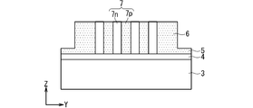
- FIG. It is sectional drawing which shows the structure of the pillar part of the silicon carbide semiconductor device which concerns on Embodiment 1.
- FIG. It is sectional drawing which shows the structure of the pillar part of the silicon carbide semiconductor device which concerns on Embodiment 1.
- FIG. It is a figure which shows the size of an n-type pillar and a p-type pillar.
- FIG. It is a perspective view which shows typically the silicon carbide semiconductor device which concerns on Embodiment 1.
- FIG. It is a figure which shows the structure of the MOSFET cell area. It is a figure which shows the structure of the MOSFET cell area.
- FIG. 1 shows the structure of the silicon carbide semiconductor device of the modification 1 of Embodiment 1.
- FIG. 2 shows the structure of the silicon carbide semiconductor device of the modification 2 of Embodiment 1.
- FIG. is sectional drawing which shows the structure of the silicon carbide semiconductor device of the modification 3 of Embodiment 1.
- FIG. 2 is sectional drawing which shows the structure of the silicon carbide semiconductor device of the modification 3 of Embodiment 1.
- FIG. It is sectional drawing which shows the structure of the silicon carbide semiconductor device of the modification 3 of Embodiment 1.
- FIG. is a perspective view schematically showing the manufacturing method of the pillar part of the silicon carbide semiconductor device which concerns on Embodiment 2.
- FIG. 2 shows the structure of the silicon carbide semiconductor device of the modification 2 of Embodiment 1.
- FIG. is sectional drawing which shows the structure of the silicon carbide semiconductor device of the modification 3
- FIG. 2 It is a perspective view schematically showing the manufacturing method of the pillar part of the silicon carbide semiconductor device which concerns on Embodiment 2.
- FIG. 2 is a perspective view schematically showing the manufacturing method of the pillar part of the silicon carbide semiconductor device which concerns on Embodiment 2.
- FIG. 2 is a perspective view schematically showing the manufacturing method of the pillar part of the silicon carbide semiconductor device which concerns on Embodiment 2.
- FIG. 2 is a perspective view schematically showing the manufacturing method of the pillar part of the silicon carbide semiconductor device which concerns on Embodiment 2.
- FIG. 1 shows the manufacturing method of the pillar part of the silicon carbide semiconductor device which concerns on Embodiment 2.
- FIG. It is sectional drawing which shows the modification 1 of the manufacturing method of the pillar part of the silicon carbide semiconductor device which concerns on Embodiment 2.
- FIG. It is sectional drawing which shows the modification 1 of the manufacturing method of the pillar part of the silicon carbide semiconductor device which concerns on Embodiment 2.
- FIG. It is sectional drawing which shows the modification 1 of the manufacturing method of the pillar part of the silicon carbide semiconductor device which concerns on Embodiment 2.
- FIG. It is sectional drawing which shows the modification 2 of the manufacturing method of the pillar part of the silicon carbide semiconductor device which concerns on Embodiment 2.
- FIG. 1 shows the manufacturing method of the pillar part of the silicon carbide semiconductor device which concerns on Embodiment 2.
- FIG. It is a perspective view which shows typically the silicon carbide semiconductor device which concerns on Embodiment 2.
- It is sectional drawing which shows the manufacturing process of the MOSFET cell of the MOSFET cell area It is sectional drawing which shows the manufacturing process of the MOSFET cell of the MOSFET cell area.
- FIG. 2 It is sectional drawing which shows the modification 2 of the manufacturing method of the silicon carbide semiconductor device which concerns on Embodiment 2.
- FIG. 2 is sectional drawing which shows the modification 2 of the manufacturing method of the silicon carbide semiconductor device which concerns on Embodiment 2.
- FIG. It is sectional drawing which shows the modification 3 of the manufacturing method of the silicon carbide semiconductor device which concerns on Embodiment 2.
- FIG. 2 is sectional drawing which shows the modification 3 of the manufacturing method of the silicon carbide semiconductor device which concerns on Embodiment 2.
- FIG. It is sectional drawing which shows the modification 4 of the manufacturing method of the silicon carbide semiconductor device which concerns on Embodiment 2.
- FIG. 1 is sectional drawing which shows the modification 2 of the manufacturing method of the silicon carbide semiconductor device which concerns on Embodiment 2.
- FIG. 2 is sectional drawing which shows the modification 2 of the manufacturing method of the silicon carbide semiconductor device
- FIG. 1 It is sectional drawing which shows the modification 5 of the manufacturing method of the silicon carbide semiconductor device which concerns on Embodiment 2.
- FIG. It is sectional drawing explaining the dicing process of two adjacent silicon carbide semiconductor devices. It is sectional drawing explaining the dicing process of two adjacent silicon carbide semiconductor devices. It is sectional drawing which shows the manufacturing method of two adjacent silicon carbide semiconductor devices. It is sectional drawing which shows the manufacturing method of two adjacent silicon carbide semiconductor devices. It is sectional drawing which shows the manufacturing method of two adjacent silicon carbide semiconductor devices. It is a perspective view schematically showing the manufacturing method of the pillar part of the silicon carbide semiconductor device which concerns on Embodiment 3.
- FIG. It is a perspective view schematically showing the manufacturing method of the pillar part of the silicon carbide semiconductor device which concerns on Embodiment 3.
- FIG. 1 It is a perspective view schematically showing the manufacturing method of the pillar part of the silicon carbide semiconductor device which concerns on Embodiment 3.
- FIG. 2 is a perspective view schematically showing the manufacturing method of the pillar part of the silicon carbide semiconductor device which concerns on Embodiment 3.
- FIG. 2 is a perspective view schematically showing the manufacturing method of the pillar part of the silicon carbide semiconductor device which concerns on Embodiment 3.
- FIG. It is a perspective view which shows typically the structure of the pillar part of the silicon carbide semiconductor device which concerns on Embodiment 3.
- FIG. It is sectional drawing which shows the manufacturing method of the pillar part of the silicon carbide semiconductor device which concerns on Embodiment 3.
- FIG. It is sectional drawing which shows the manufacturing method of the pillar part of the silicon carbide semiconductor device which concerns on Embodiment 3.
- FIG. It is sectional drawing which shows the manufacturing method of the pillar part of the silicon carbide semiconductor device which concerns on Embodiment 3.
- FIG. It is sectional drawing which shows the manufacturing method of the pillar part of the silicon carbide semiconductor device which concerns on Embodiment 3.
- FIG. It is sectional drawing which shows the manufacturing method of the pillar part of the silicon carbide semiconductor device which concerns on Embodiment 3.
- FIG. It is sectional drawing which shows the manufacturing method of the pillar part of the silicon carbide semiconductor device which concerns on Embodiment 3.
- FIG. It is sectional drawing which shows the manufacturing method of the pillar part of the silicon carbide semiconductor device which concerns on Embodiment 3.
- FIG. It is sectional drawing which shows the manufacturing method of the pillar part of the silicon carbide semiconductor device which concerns on Embodiment 3.
- FIG. It is sectional drawing which shows the manufacturing method of the pillar
- FIG. It is a perspective view which shows typically the silicon carbide semiconductor device which concerns on Embodiment 3.
- FIG. It is sectional drawing which shows the manufacturing process of the MOSFET cell of the MOSFET cell area. It is sectional drawing which shows the manufacturing process of the MOSFET cell of the MOSFET cell area. It is sectional drawing which shows the manufacturing process of the MOSFET cell of the MOSFET cell area. It is sectional drawing which shows the manufacturing process of the MOSFET cell of the MOSFET cell area. It is sectional drawing which shows the manufacturing process of the MOSFET cell of the MOSFET cell area. It is sectional drawing which shows the manufacturing process of the MOSFET cell of the MOSFET cell area.
- FIG. It is sectional drawing which shows the modification 2 of the manufacturing method of the silicon carbide semiconductor device which concerns on Embodiment 3.
- FIG. It is sectional drawing which shows the modification 3 of the manufacturing method of the silicon carbide semiconductor device which concerns on Embodiment 3.
- FIG. It is sectional drawing which shows the modification 3 of the manufacturing method of the silicon carbide semiconductor device which concerns on Embodiment 3.
- FIG. It is sectional drawing which shows the modification 4 of the manufacturing method of the silicon carbide semiconductor device which concerns on Embodiment 3.
- FIG. It is sectional drawing which shows the modification 5 of the manufacturing method of the silicon carbide semiconductor device which concerns on Embodiment 3.
- FIG. It is sectional drawing which shows the modification 5 of the manufacturing method of the silicon carbide semiconductor device which concerns on Embodiment 3.
- FIG. It is sectional drawing which shows the modification 5 of the manufacturing method of the silicon carbide semiconductor device which concerns on Embodiment 3.
- the semiconductor device in each embodiment described below refers to a semiconductor chip obtained by separating a semiconductor device manufactured through a wafer process into chip units by a dicing process, and the chip peripheral portion is a semiconductor chip. It shall refer to the outer peripheral part of.
- the "outside” is the direction toward the outer circumference of the semiconductor chip, and the “inside” is the direction opposite to the "outside”.
- the n-type is generally defined as the "first conductive type”
- the p-type opposite to the n-type is generally defined as the "second conductive type”, but vice versa. It does not matter if it is defined as.
- the n - type indicates that the impurity concentration is lower than that of the n-type
- the n + type indicates that the impurity concentration is higher than that of the n-type.
- p - type indicates that the impurity concentration is lower than that of p-type
- p + type indicates that the impurity concentration is higher than that of p-type.
- top, bottom, side, bottom, front or back may be used to mean a specific position and direction.
- the term is used for convenience in order to facilitate understanding of the contents of the embodiment, and has nothing to do with the direction in which it is actually implemented.
- MOS metal-oxide-semiconductor junction structures
- MOSFET field effect transistor
- polycrystalline silicon has been adopted as a material for gate electrodes instead of metal, mainly from the viewpoint of forming source and drain in a self-aligned manner.
- a material having a high dielectric constant is adopted as the material of the gate insulating film, but the material is not necessarily limited to the oxide.
- MOS is not necessarily limited to the metal-oxide-semiconductor laminated structure, and the present specification does not presuppose such limitation. That is, in view of common general technology, "MOS” has a meaning not only as an abbreviation derived from the etymology but also broadly including a conductor-insulator-semiconductor laminated structure.
- FIG. 1 is a perspective view schematically showing the configuration of a pillar portion of a silicon carbide semiconductor device 100 having an SJ structure as the semiconductor device according to the first embodiment.
- the silicon carbide semiconductor device 100 shows a vertical MOSFET in which a main current flows in a direction perpendicular to the main surface of the semiconductor substrate, but for convenience, the main electrode, the unit cell of the MOSFET, and the like are omitted from the illustration. There is.
- the pillar portion 7 has a plurality of n-type pillars 7n (first pillars) having a striped plan view shape and a plurality of p-type pillars 7p (second pillars), respectively. It is a region alternately arranged on the semiconductor substrate 3 so as to be parallel in the width direction orthogonal to the longitudinal direction of the above. These arrangement directions are orthogonal to the direction in which the main current of the silicon carbide semiconductor device 100 flows.
- a p-type pillar peripheral portion 6 containing a p-type impurity is provided so as to surround the pillar portion 7, and the outer side of the p-type pillar peripheral portion 6 is a p-type chip peripheral portion 5 containing a p-type impurity.
- the semiconductor substrate 3 is an n + type SiC substrate, for example, a commercially available 4H-SiC n-type substrate having an off angle of 4 degrees in the [11-20] direction and having an off angle of 300 to 400 ⁇ m. It has a thickness and the concentration of n-type impurities is 5 ⁇ 10 18 to 1 ⁇ 10 20 cm -3 .
- An n-type SiC layer 4 (first semiconductor layer) containing n-type impurities is provided between the semiconductor substrate 3 and the p-type chip peripheral portion 5, and the thickness thereof is 0.5 to 10 ⁇ m and the n-type.
- the concentration of impurities is 1 ⁇ 10 14 to 5 ⁇ 10 19 cm -3 .
- the semiconductor substrate 3 and the n-type SiC layer 4 may be collectively referred to as a semiconductor substrate.
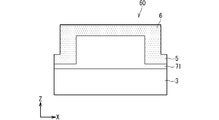
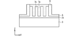
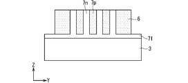
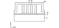
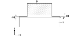
- FIG. 2 A cross-sectional view in the arrow direction along the AA line (line parallel to the Y axis) in FIG. 1 is shown in FIG. 2, and a cross-sectional view in the arrow direction along the BB line (line parallel to the X axis) is shown in FIG. It is shown in FIG.
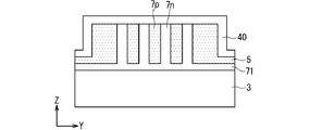
- the n-type pillars 7n and the p-type pillars 7p are provided so as to project from the n-type SiC layer 4 in the height direction (Z-axis direction), and the p-type pillar peripheral portion 6 is provided.
- the pillar portion 7 is surrounded, and the p-type chip peripheral portion 5 covers the outer periphery of the n-type SiC layer 4.
- the end face of the n-type SiC layer 4 is exposed on the side surface of the semiconductor chip.
- FIG. 4 is a diagram showing the sizes of the n-type pillars 7n and the p-type pillars 7p, and the pillar width 7nW of the n-type pillars 7n and the pillar width 7pW of the p-type pillars 7p are equivalent to each other, for example, 0. It is formed to a length of 5 to 5 ⁇ m. Further, the pillar height 7nH of the n-type pillar 7n and the pillar width 7pH of the p-type pillar 7p are equivalent to each other, and are formed at a height of, for example, 5 to 100 ⁇ m.
- the product of the impurity concentration and the width of the n-type pillar 7n is formed so as to substantially match the product of the impurity concentration and the width of the p-type pillar 7p, and the concentrations of the n-type impurity and the p-type impurity are, for example, 5 ⁇ , respectively. It is 10 15 to 1 ⁇ 10 18 cm -3 . With such a configuration, when the silicon carbide semiconductor device 100 is off, the depletion layer spreads over the entire n-type pillar 7n and p-type pillar 7p.
- the impurity concentration of the n-type SiC layer 4 should be the same as or lower than the impurity concentration of the n-type pillar 7n, but the impurities of the n-type pillar 7n.
- the concentration can be higher than the concentration.
- the n-type pillars 7n and the p-type pillars 7p can be directly bonded to the semiconductor substrate 3 without providing the n-type SiC layer 4.
- the impurity concentration of the n-type SiC layer 4 is higher than the impurity concentration of the n-type pillar 7n, or when the n-type SiC layer 4 is not provided, the impurity concentration of the n-type SiC layer 4 is n-type.
- the effect is smaller than when the impurity concentration of the pillar 7n is the same or lower, by providing the pillar portion 7 as shown in FIG. 1, a silicon carbide semiconductor device having a higher breakdown voltage and lower resistance than the conventional structure is provided. Can be realized.
- FIGS. 1 to 4 show a configuration in which the pillar portion 7 is provided with three p-type pillars 7p and four n-type pillars 7n, the number actually corresponds to the size of the carbonized semiconductor device.
- the p-type pillar 7p and the n-type pillar 7n are formed.
- the pillar width is 0.5 to 5 ⁇ m, and the width of the entire MOSFET cell region in which the MOSFET unit cell is provided in the Y direction is, for example, 1 to 10 mm, so that at least in the MOSFET cell region.
- a number of p-type pillars 7p and n-type pillars 7n that can be accommodated are formed.
- the width 6W of the p-type pillar peripheral portion 6 is made thicker than the width 7pW of the p-type pillar 7p, so that the p-type pillar peripheral portion 6 and the p-type pillar 7p are formed.
- the product of the impurity concentration and the width of the p-type pillar peripheral portion 6 becomes larger than the product of the impurity concentration and the width of the p-type pillar 7p.
- the depletion layer does not spread over the entire p-type pillar peripheral portion 6, the electric field strength of the p-type pillar peripheral portion 6 is suppressed to a low level, and an increase in leakage current and a discharge risk are suppressed.
- the width of the p-type pillar peripheral portion 6 can be 1.2 times or more the width of the p-type pillar 7p.
- the impurity concentration of the p-type pillar peripheral portion 6 is set to 1.2 times or more the impurity concentration of the p-type pillar 7p.
- the depletion layer does not spread over the entire p-type pillar peripheral portion 6, the electric field strength of the p-type pillar peripheral portion 6 is suppressed to a low level, and the increase in leakage current and the discharge risk are suppressed.
- FIG. 5 is a perspective view of a silicon carbide semiconductor device 100 schematically showing a MOSFET cell region MCR when a MOSFET unit cell is provided in the pillar portion 7 and a MOSFET terminal region MTR provided on the outer periphery thereof.
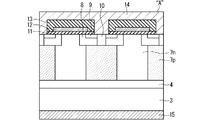
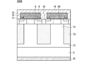
- FIG. 6 is a cross-sectional view taken along the line CC (a line parallel to the Y axis) in FIG. 5 in the direction indicated by the arrow, and FIG. 7 shows an enlarged view of the region A in FIG.
- the MOSFET is provided with an n-type SiC layer 4 on one main surface of the semiconductor substrate 3, and a plurality of p-type pillars 7p and a plurality of n-type pillars 7n on the n-type SiC layer 4. Are provided alternately.
- a plurality of p-type well regions 8 are selectively provided from the upper layer portion of the p-type pillar 7p to the upper layer portion of the n-type pillar 7n, and each well region 8 is provided with a p-type contact region 10 well. It is provided so as to penetrate the region 8.
- An n-type source region 9 is provided in the upper layer of the well region 8 in contact with both side surfaces of the contact region 10.
- the thickness of the source region 9 is thinner than the thickness of the well region 8, the thickness of the contact region 10 is about the same as the thickness of the well region 8, or the contact region 10 is provided so as to be slightly deeper. It is configured to be electrically connected to the pillar 7p.
- the gate insulating film 11 is selectively formed so as to straddle the source region 9 of the adjacent well regions 8, and the gate electrode 12 is formed on the gate insulating film 11. That is, the gate insulating film 11 is formed between the adjacent source regions 9 from a part of the source region 9 on the well region 8 and on the n-type pillar 7n to a part of the source region 9 of the adjacent well regions 8. It is provided so as to cross, and the gate electrode 12 is provided on the gate insulating film 11.
- the interlayer insulating film 13 is formed so as to cover the gate insulating film 11 and the gate electrode 12, and the source electrode 14 is formed so as to cover the interlayer insulating film 13.
- the interlayer insulating film 13 is provided with a contact hole in a region other than the region covering the gate electrode 12, which penetrates the interlayer insulating film 13 in the thickness direction and reaches a part of the source region 9 and the entire surface of the contact region 10. Has been done.
- the contact hole is filled with the source electrode 14, and the source electrode 14 is connected to the source region 9 and the contact region 10.
- drain electrode 15 is provided on the other main surface (back surface) of the semiconductor substrate 3 on the side opposite to the side where the source electrode 14 is provided.
- An example of the configuration of the MOSFET cell region MCR and the MOSFET termination region MTR will be further described later.
- the p-type pillars are provided on the semiconductor substrate 3 by providing the pillar portions 7 in which a plurality of n-type pillars 7n having a striped shape in a plan view and a plurality of p-type pillars 7p are alternately arranged.
- 7p is formed by epitaxial growth, voids are not formed and the ineffective region can be reduced. Therefore, processing for separating the void becomes unnecessary, and the manufacturing cost can be reduced.
- FIG. 7 a configuration in which two MOSFET unit cells are provided is shown, but in reality, a number of unit cells are formed according to the size of the carbonized semiconductor device.
- FIG. 8 is a cross-sectional view showing the configuration of the silicon carbide semiconductor device 100A of the first modification of the first embodiment, and is a cross-sectional view corresponding to FIG. 7. As shown in FIG. 8, in the silicon carbide semiconductor device 100A, instead of providing the n-type SiC layer 4, an n-type SiC layer 40 (second n-type SiC layer) is provided between the well regions 8.
- FIG. 9 is a cross-sectional view showing the configuration of the silicon carbide semiconductor device 100B of the second modification of the first embodiment, and is a cross-sectional view corresponding to FIG. 2. As shown in FIG. 9, the silicon carbide semiconductor device 100B has a configuration in which the p-type chip peripheral portion 5 is not provided on the n-type SiC layer 4.
- Such a configuration has a feature that it is easy to make when the p-type pillar 7p is formed by the embedded epi method and when the p-type pillar 7p is formed by full-scale etching.
- the n-type SiC layer 4 has a uniform thickness, but the thickness of the n-type SiC layer 4 in the region where the p-type chip peripheral portion 5 is removed is the p-type pillar peripheral portion 6 and p. It can be made smaller than the thickness of the lower part of the mold pillar 7p.
- ⁇ Modification 3> 10 and 11 are cross-sectional views showing the configuration of the silicon carbide semiconductor device 100C of the modification 3 of the first embodiment, and are cross-sectional views corresponding to FIGS. 2 and 3, respectively.
- the pillar peripheral portion height 4H2 of the n-type SiC layer 4 is lower than the pillar height 4H1 of the n-type SiC layer 4 in the pillar portion 7. ..
- FIG. 12 is a diagram schematically showing the flow of the main current in the MOSFET cell region MCR when such a configuration is adopted by arrows.
- the main current in the MOSFET cell region MCR flows in the MOSFET cell region MCR, and it is difficult for the current to flow in the peripheral portion of the chip.
- the thickness of the pillar peripheral portion of the n-type SiC layer 4 becomes thin, so that the current path becomes narrower, and the spread width of the main current to the chip peripheral portion becomes narrower, which is mainly before spreading to the chip peripheral portion.
- the ratio of the height 4H1 to the height 4H2 can be, for example, about 2: 1.
- the peripheral part of the chip has defects during dicing, etc., and problems are likely to occur when the main current flows.
- the current withstand capacity increases when a large current flows.
- a silicon carbide semiconductor device using silicon carbide as a semiconductor can obtain a semiconductor device having excellent withstand voltage, high allowable current density, excellent heat resistance, and high temperature operation as compared with a semiconductor device using silicon as a semiconductor. Can be done.
- ⁇ Embodiment 2> ⁇ Manufacturing method of pillar part>
- a method of manufacturing the pillar portion of the silicon carbide semiconductor device 200 will be described.
- a commercially available 4H-SiC n-type substrate having an off angle of 4 degrees in the [11-20] direction and a thickness of 300 to 400 ⁇ m.
- a semiconductor substrate 3 having a concentration of n-type impurities of 5 ⁇ 10 18 to 1 ⁇ 10 20 cm -3 is prepared.
- an n-type SiC layer 70 (first semiconductor layer) containing an n-type impurity is formed on one main surface of the semiconductor substrate 3 by epitaxial growth.
- the n-type SiC layer 70 may have a thickness of, for example, 5 to 100 ⁇ m, and the impurity concentration may be 1 ⁇ 10 15 to 1 ⁇ 10 18 cm -3 .
- the semiconductor substrate 3 and the n-type SiC layer 70 may be collectively referred to as a semiconductor substrate.
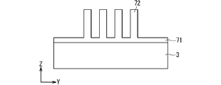
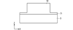
- the n-type SiC layer 70 is etched by dry etching to form the convex portion 72 of the n-type SiC layer 70 and the n-type chip peripheral portion 71 of the n-type SiC layer 70.
- the convex portion 72 has a plan view shape extending in a direction parallel to the X axis ([11-20] direction). It is formed in a striped shape so that a plurality of convex portions 72 are arranged at intervals in a direction along the Y axis ([1-100] direction).
- the shape of the p-type SiC layer is changed when the p-type SiC layer is formed between the convex portions 72 by epitaxial growth. It becomes easier to control.
- the convex portion 72 is formed in a range where the width in the Y-axis direction is, for example, 0.5 to 5 ⁇ m, and the height in the Z-axis ([0001] direction) direction is, for example, 5 to 100 ⁇ m.
- the striped convex portion 72 can be formed in an direction rotated by 90 degrees around the [0001] axis from the [11-20] direction. .. That is, even if the convex portion 72 is formed in the direction in which the [11-20] axis and the [1-100] axis are exchanged in FIG. 15, the p-type SiC layer formed between the convex portions 72 by epitaxial growth has a symmetrical shape. Therefore, it becomes easy to control the shape of the p-type SiC layer.
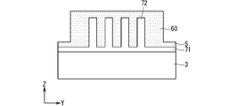
- the p-type SiC layer 60 (second semiconductor layer) is formed by epitaxial growth so as to cover the n-type chip peripheral portion 71 and the convex portion 72 of the n-type SiC layer 70.
- the surface of the p-type SiC layer 60 of the convex portion 72 of the n-type SiC layer 70 is flat, but may have irregularities.
- the difference in crystal plane orientation can be obtained. Voids are not formed due to the difference in crystal growth rate due to the difference, and the ineffective region can be reduced. Therefore, processing for separating the void becomes unnecessary, and the manufacturing cost can be reduced.
- the concentration of p-type impurities in the p-type SiC layer 60 may be set so that the product of the impurity concentration of the n-type pillar 7n and the width substantially matches the product of the impurity concentration and the width of the p-type pillar 7p.
- the p-type SiC layer 60 on the convex portion 72 of the n-type SiC layer 70 is removed by polishing or dry etching to expose the upper surface of the convex portion 72 and between the convex portions 72.
- the p-type SiC layer 60 is left in the.
- the convex portion 72 becomes an n-type pillar 7n
- the p-type SiC layer 60 between the convex portions 72 becomes a p-type pillar 7p to form the pillar portion 7.
- a p-type pillar peripheral portion 6 having a predetermined width is formed so as to surround the pillar portion 7.
- the upper part of the convex portion 72 of the n-type SiC layer 70 can be partially removed.
- the upper part of the p-type chip peripheral portion 5 on the n-type chip peripheral portion 71 of the n-type SiC layer 70 can be partially removed.
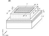
- FIG. 18 shows a perspective view of the silicon carbide semiconductor device 200 formed by the above method before the MOSFET cell region MCR and the MOSFET terminal region MTR are formed.
- the silicon carbide semiconductor device 200 it is shown in FIG. 1 except that the end surface of the n-type chip peripheral portion 71 of the n-type SiC layer 70 is exposed on the side surface of the semiconductor chip. It is the same as the silicon carbide semiconductor device 100.
- FIGS. 14 to 18 show a configuration in which the pillar portion 7 is provided with three p-type pillars 7p and four n-type pillars 7n, the number actually corresponds to the size of the carbonized semiconductor device.
- the p-type pillar 7p and the n-type pillar 7n are formed.
- FIG. 19 is a cross-sectional view taken along the line AA in the process shown in FIG.
- the cross-sectional view taken along the line BB is the same as that in FIG.
- FIG. 20 is a cross-sectional view taken along the line AA in the process shown in FIG. 15, and
- FIG. 21 is a cross-sectional view taken along the line BB.
- 22 is a cross-sectional view taken along the line AA in the process shown in FIG. 16, and
- FIG. 23 is a cross-sectional view taken along the line BB.
- FIG. 24 is a cross-sectional view taken along the line AA in the process shown in FIG. 17, and
- FIG. 25 is a cross-sectional view taken along the line BB.
- an n-type SiC layer 4 containing an n-type impurity is formed on one main surface of the semiconductor substrate 3 by epitaxial growth, and further formed on the n-type SiC layer 4 by epitaxial growth.
- An n-type SiC layer 70 containing an n-type impurity can be formed to form a two-layer structure.
- the n-type SiC layer 4 to be the first layer has a thickness of, for example, 0.5 to 10 ⁇ m, and the concentration of n-type impurities is 1 ⁇ 10 14 to 1 ⁇ 10 19 cm -3, and the n-type SiC layer 4 to be the second layer is n.
- the type SiC layer 70 can have a thickness of, for example, 5 to 100 ⁇ m and a concentration of n-type impurities of 1 ⁇ 10 15 to 1 ⁇ 10 18 cm -3 . Both the n-type SiC layer 4 and the n-type SiC layer 70 can be referred to as a first n-type SiC layer.
- the first n-type SiC layer into a two-layer structure in this way, it is possible to alleviate the strain due to the difference in the lattice constant of the crystal due to the difference in the impurity concentration between the semiconductor substrate 3 and the epitaxial layer. can.
- the thickness and the impurity concentration are changed between the first layer and the second layer because the thickness and the impurity concentration required for relaxing the strain are different between the first layer and the second layer.
- the peripheral portion of the first n-type SiC layer is 1 of the n-type SiC layer 4 with respect to the configuration shown in FIG.
- the thickness of the n-type SiC layer 4 which is only one layer can be reduced.
- a part of the second n-type SiC layer 70 can be left in the peripheral portion of the first n-type SiC.
- the first n-type SiC under the convex portion 72 is formed by etching so that over-etching does not occur. That is, the structure can be such that the n-type SiC layer 70 does not remain. With such a configuration, the bottom of the pillar comes into contact with the semiconductor substrate 3 having a high impurity concentration, so that the resistance can be reduced and the electric field balance is maintained as compared with the configuration shown in FIG. 29. Easy to design.
- FIG. 31 is a perspective view of a silicon carbide semiconductor device 200 schematically showing a MOSFET cell region MCR when a MOSFET unit cell is provided in the pillar portion 7 and a MOSFET terminal region MTR provided on the outer periphery thereof.
- FIGS. 32 to 35 The manufacturing process of the MOSFET cell in the MOSFET cell region MCR will be described with reference to FIGS. 32 to 35.
- 32 is a cross-sectional view corresponding to FIG. 24, and an enlarged view of the region B in FIG. 32 is shown in FIG. 33.
- FIG. 33 the same components as those described with reference to FIG. 7 are designated by the same reference numerals, and duplicate description will be omitted.
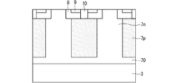
- an n-type SiC layer 70 is provided on one main surface of the semiconductor substrate 3, and a plurality of p-type pillars 7p and a plurality of n-type pillars 7n alternate on the n-type SiC layer 70. It is provided in. Then, a plurality of p-type well regions 8 are selectively formed by ion implantation of p-type impurities from the upper layer portion of the p-type pillar 7p to the upper layer portion of the n-type pillar 7n. Further, in each well region 8, a p-type contact region 10 is formed by ion implantation of a p-type impurity so as to penetrate the well region 8.
- an n-type source region 9 is formed in the upper layer of the well region 8 by ion implantation of an n-type impurity so as to be in contact with both side surfaces of the contact region 10.
- activation annealing is performed to activate the implanted impurities.
- the thickness of the p-type well region 8 is, for example, 0.2 to 1.5 ⁇ m
- the concentration of the p-type impurity is, for example, 1 ⁇ 10 14 to 1 ⁇ 10 19 cm -3
- the thickness of the source region 9 is set.
- the concentration of n-type impurities is, for example, 1 ⁇ 10 17 to 1 ⁇ 10 21 cm -3
- the thickness of the contact region 10 is, for example, 0.2 to 1.5 ⁇ m.
- the concentration of the p-type impurity can be, for example, 1 ⁇ 10 18 to 1 ⁇ 10 21 m -3 .
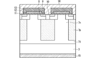
- an insulating film used as a material for the gate insulating film 11, for example, a silicon oxide film 111 is formed on the pillar portion 7, and a conductor film serving as a gate electrode 12 is further formed on the silicon oxide film 111.
- a polysilicon film is formed.
- the polysilicon film is patterned to form the gate electrode 12 so as to straddle the upper edge portion of the adjacent source regions 9.
- an insulating film as a material of the interlayer insulating film 13 for example, a silicon oxide film 131 is formed so as to cover the gate electrode 12 and the silicon oxide film 111.
- the silicon oxide films 111 and 131 are patterned to form the interlayer insulating film 13 that covers the gate insulating film 11 and the gate electrode 12.
- a contact hole is formed which penetrates the interlayer insulating film 13 in the thickness direction and reaches a part of the source region 9 and the entire surface of the contact region 10.
- the inside of the contact hole is embedded and a conductor film is formed so as to cover the interlayer insulating film 13 to form the source electrode 14, and the other side of the semiconductor substrate 3 on the opposite side to the side where the source electrode 14 is provided.
- the drain electrode 15 on the main surface (back surface) of the silicon carbide semiconductor device 200, the silicon carbide semiconductor device 200 is completed.
- An example of a method for manufacturing the MOSFET cell region MCR and the MOSFET terminal region MTR will be further described later.
- a plurality of p-type well regions 8 are selectively provided from the upper layer portion of the p-type pillar 7p to the upper layer portion of the n-type pillar 7n, and each well region 8 is provided.
- the configuration in which the p-type contact region 10 and the n-type source region 9 are provided is shown in the above, the p-type well region 8 and the like are not provided in the upper layer of the n-type pillar 7n and the p-type pillar 7p.
- the n-type SiC layer 40 (third semiconductor layer) may be provided on the n-type pillars 7n and the p-type pillars 7p, and the p-type well region 8 or the like may be provided in the n-type SiC layer 40. can.
- the manufacturing process will be described with reference to FIGS. 36 to 40 as another example of the method for manufacturing the semiconductor device.
- the n-type SiC layer 40 is formed by epitaxial growth so as to cover the region from the pillar portion 7 to the p-type chip peripheral portion 5.
- the n-type SiC layer 40 can be formed on the entire surface of the semiconductor chip, can be formed only in the MOSFET cell region in which the MOSFET cell is formed, or can be formed in the MOSFET cell region and the MOSFET terminal region.
- FIG. 37 is a drawing showing an enlarged area of FIG. 36, and an enlarged view of the area C in FIG. 37 is shown in FIG. 38.
- FIG. 38 the same components as those described with reference to FIG. 7 are designated by the same reference numerals, and duplicate description will be omitted.
- a plurality of p-type well regions 8 are selectively formed in the n-type SiC layer 40 from above the p-type pillar 7p to above the n-type pillar 7n by ion implantation of p-type impurities. .. Further, in each well region 8, a p-type contact region 10 is formed by ion implantation of a p-type impurity so as to penetrate the well region 8. Further, an n-type source region 9 is formed in the upper layer of the well region 8 by ion implantation of an n-type impurity so as to be in contact with both side surfaces of the contact region 10. In order to recover the crystal defects formed by ion implantation, activation annealing is performed to activate the implanted impurities.
- an insulating film used as a material for the gate insulating film 11, for example, a silicon oxide film 111 is formed on the n-type SiC layer 40, and further, a gate electrode 12 is formed on the silicon oxide film 111.
- a conductor film, for example a polysilicon film, is formed.
- the polysilicon film is patterned to form the gate electrode 12 so as to straddle the upper edge portion of the adjacent source regions 9.
- an insulating film as a material of the interlayer insulating film 13, for example, a silicon oxide film 131 is formed so as to cover the gate electrode 12 and the silicon oxide film 111.
- the silicon oxide films 111 and 131 are patterned to form the interlayer insulating film 13 that covers the gate insulating film 11 and the gate electrode 12.
- a contact hole is formed which penetrates the interlayer insulating film 13 in the thickness direction and reaches a part of the source region 9 and the entire surface of the contact region 10.
- the inside of the contact hole is embedded and a conductor film is formed so as to cover the interlayer insulating film 13 to form the source electrode 14, and the other side of the semiconductor substrate 3 on the opposite side to the side where the source electrode 14 is provided.
- the drain electrode 15 on the main surface (back surface) of the silicon carbide semiconductor device 200A, the silicon carbide semiconductor device 200A is completed.
- the thickness of the p-type well region 8 and the thickness of the n-type SiC layer 40 were made equal, but as shown in FIG. 41, the p-type well region 8 was formed. It can be formed deeper than the thickness of the n-type SiC layer 40. With such a configuration, the corners of the p-type well region 8 do not come into contact with the high-concentration n-type SiC layer 40, and the electric field at the corners of the p-type well region 8 when a high voltage is applied to the MOSFET. The strength can be reduced and the withstand voltage can be maintained.
- the depth of the p-type well region 8 is set to be about 0.1 to 1 ⁇ m in thickness of the n-type SiC layer 40.
- voids are not formed when the p-type pillar 7p is formed by epitaxial growth, and the ineffective region can be reduced. Therefore, processing for separating the void becomes unnecessary, and the manufacturing cost can be reduced.
- FIGS. 35 and 40 a configuration in which two MOSFET unit cells are provided is shown, but in reality, a number of unit cells are formed according to the size of the carbonized semiconductor device.
- n-type SiC layer 70 n is subjected to epitaxial growth.
- the p-type SiC layer 60 is formed so as to cover the mold chip peripheral portion 71 and the convex portion 72, the p-type SiC layer 60 is placed between the convex portions 72 of the n-type SiC layer 70 as shown in FIGS. 42 and 43.
- the width 6W of the p-type pillar peripheral portion 6 is formed to be significantly larger than the width 7pW of the p-type pillar 7p.
- the product of the impurity concentration and the width of the p-type pillar peripheral portion 6 is larger than the product of the impurity concentration and the width of the p-type pillar 7p. It will be significantly larger. With such a configuration, the depletion layer does not spread over the entire p-type pillar peripheral portion 6, the electric field strength of the p-type pillar peripheral portion 6 is suppressed to a low level, and an increase in leakage current and a discharge risk are suppressed.
- FIGS. 44 and 45 are views corresponding to FIGS. 22 and 23, respectively.
- n-type SiC layer 70 n is subjected to epitaxial growth.
- the p-type SiC layer 60 is formed so as to cover the mold chip peripheral portion 71 and the convex portion 72, as shown in FIGS. 44 and 45, the p-type impurity concentration of the p-type pillar peripheral portion 6 is p-type. It is formed so as to be higher than the p-type impurity concentration of the pillar 7p.
- the epitaxial conditions of the p-type SiC layer 60 are adjusted so that the p-type pillar peripheral portion 6 is more likely to take in the p-type impurities than the protrusions 72 of the n-type SiC layer 70.
- the p-type pillar peripheral portion 6 is substantially limited to crystal growth from the bottom surface of the trench, but the amount of impurities taken up differs between the convex portions 72 because the crystals grow from the plurality of surfaces of the bottom surface of the trench and the side wall of the trench.
- the ease of supply of raw material gas and impurity gas differs between the p-type pillar peripheral portion 6 dug down in a wide area and the convex portion 72 dug down in a narrow width, so these factors are used.
- the epitaxial conditions of the p-type SiC layer 60 are adjusted in consideration.
- the product of the impurity concentration and the width of the p-type pillar peripheral portion 6 is the impurity concentration and width of the p-type pillar 7p. Is greater than the product of.
- the product of the impurity concentration and the width of the p-type pillar peripheral portion 6 is obtained from the product of the impurity concentration and the width of the p-type pillar 7p. Can also be made significantly larger. With such a configuration, the depletion layer does not spread over the entire p-type pillar peripheral portion 6, the electric field strength of the p-type pillar peripheral portion 6 is suppressed to a low level, and an increase in leakage current and a discharge risk are suppressed.
- FIGS. 46 and 47 are views corresponding to FIGS. 22 and 23, respectively.
- n-type SiC layer 70 n is subjected to epitaxial growth.
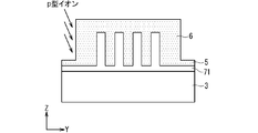
- ion injection of the p-type impurity is performed into the p-type pillar peripheral portion 6 as shown in FIGS. 46 and 47, and p.
- the concentration of p-type impurities in the peripheral portion 6 of the mold pillar is set to be higher than the concentration of p-type impurities in the p-type pillar 7p.
- the product of the impurity concentration and the width of the p-type pillar peripheral portion 6 becomes larger than the product of the impurity concentration and the width of the p-type pillar 7p.
- the depletion layer does not spread over the entire p-type pillar peripheral portion 6, the electric field strength of the p-type pillar peripheral portion 6 is suppressed to a low level, and an increase in leakage current and a discharge risk are suppressed.
- ion implantation into the p-type pillar peripheral portion 6 can be performed only at necessary locations.
- the epitaxial growth rate and the epitaxial concentration may differ depending on the crystal orientation.
- the product of the impurity concentration and the width of the p-type pillar peripheral portion 6 may not be uniformly formed, and the product of the impurity concentration and the width of the p-type pillar peripheral portion 6 may be formed.
- a place smaller than the product of the impurity concentration and the width of the p-type pillar 7p may be formed.
- ion injection is performed only in the portion where the product of the concentration and width of the p-type pillar peripheral portion 6 is smaller than the product of the impurity concentration and width of the p-type pillar peripheral portion 6, and the concentration and width of the p-type pillar peripheral portion 6 are The product can be larger than the product of the impurity concentration and the width of the p-type pillar peripheral portion 6.
- the semiconductor device has the same structure and size, a place where the product of the impurity concentration and the width of the p-type pillar peripheral portion 6 is smaller than the product of the impurity concentration and the width of the p-type pillar 7p always occurs in the same place. Therefore, it can be specified by making a sample, disassembling it, and verifying it.
- the reason why the product of the impurity concentration and the width of the p-type pillar peripheral portion 6 becomes smaller than the product of the impurity concentration and the width of the p-type pillar 7p is that the width of the p-type pillar peripheral portion 6 is narrow depending on the epitaxial condition. It is conceivable that the amount of p-type impurities taken up by the crystal plane is small and the concentration of p-type impurities is low.
- FIG. 48 is a diagram corresponding to FIG. 24.
- the p-type chip peripheral portion 5 can be removed at the same time as the p-type SiC layer 60 on the convex portion 72 of the p-type SiC layer 60 by full surface etching, and the manufacturing process can be simplified. At this time, a part of the n-type chip peripheral portion 71 of the n-type SiC layer 70 can also be removed.
- FIGS. 49 and 50 are views corresponding to FIGS. 20 and 21, respectively.
- the thickness of the n-type SiC layer 4 which is only one layer is reduced. You can also do it. As a result, the height 4H2 of the pillar peripheral portion of the n-type SiC layer 4 is lower than the height 4H1 of the n-type SiC layer 4 in the pillar portion 7.
- FIGS. 51 and 52 correspond to a cross-sectional view showing adjacent silicon carbide semiconductor devices 200 in a wafer state
- FIG. 51 is a cross-sectional view taken along the line AA of FIG. 18,
- FIG. 52 is a cross-sectional view taken along the line AA.
- the silicon carbide semiconductor device 200 is in the state shown in FIG. 35, but the source electrode 14, the drain electrode 15, and the like are omitted.
- dicing is performed at the position indicated by the arrow between the two silicon carbide semiconductor devices 200 to separate them into chip units.
- the distance between the convex portions 72 of the n-type SiC layer 70 is compared with the pillar width of 0.5 to 5 ⁇ m of the n-type pillar 7n and the p-type pillar 7p. It is 10 times or more, for example, 50 ⁇ m or more.
- FIGS. 53 and 54 show the convex portion 72 of the n-type SiC layer 70 in the process shown in FIG. 20, and FIGS. 53 and 54 correspond to FIGS. 51 and 52, respectively.
- d1 the distance between the convex portions 72 in the adjacent silicon carbide semiconductor devices
- d2 the distance between the convex portions 72 in the adjacent silicon carbide semiconductor devices
- a method of manufacturing the pillar portion of the silicon carbide semiconductor device 300 will be described.
- a commercially available 4H-SiC n-type substrate having an off angle of 4 degrees in the [11-20] direction and having an off angle of 300 to 400 ⁇ m.
- a semiconductor substrate 3 having a thickness of 5 ⁇ 10 18 to 1 ⁇ 10 20 cm -3 with an n-type impurity concentration.
- an n-type SiC layer 4 (semiconductor layer) containing n-type impurities is formed on one main surface of the semiconductor substrate 3 by epitaxial growth.
- the n-type SiC layer 4 may have a thickness of, for example, 0.5 to 10 ⁇ m, and the impurity concentration may be 1 ⁇ 10 14 to 1 ⁇ 10 19 cm -3 . It is also possible to omit the formation of the n-type SiC layer 4.
- a p-type SiC layer 60 (first semiconductor layer) containing p-type impurities is formed on the n-type SiC layer 4 by epitaxial growth.
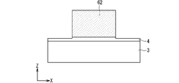
- the p-type SiC layer 60 is etched by dry etching to form the convex portion 62 of the p-type SiC layer 60, and the p-type SiC layer 60 around the convex portion 62 is removed. Then, the surface of the peripheral portion of the n-type SiC layer 4 is exposed. At this time, a part of the n-type SiC layer 4 can be removed to form irregularities on the surface of the n-type SiC layer 4.
- the convex portion 62 has a plan view shape extending in a direction parallel to the X axis ([11-20] direction). It is formed in a striped shape so that a plurality of convex portions 62 are arranged at intervals in a direction along the Y axis ([1-100] direction). Since the p-type SiC layer 60 has a symmetrical shape in the direction perpendicular to the [11-20] direction, the shape of the n-type SiC layer is changed when the n-type SiC layer is formed between the convex portions 62 by epitaxial growth. It becomes easier to control.
- the convex portion 62 is formed in a range where the width in the Y-axis direction is, for example, 0.5 to 5 ⁇ m, and the height in the Z-axis ([0001] direction) direction is, for example, 5 to 100 ⁇ m.
- the striped convex portion 62 can be formed in an direction rotated by 90 degrees around the [0001] axis from the [11-20] direction. .. That is, even if the convex portion 62 is formed in the direction in which the [11-20] axis and the [1-100] axis are exchanged in FIG. 57, the n-type SiC layer formed between the convex portions 62 by epitaxial growth has a symmetrical shape. Therefore, it becomes easy to control the shape of the n-type SiC layer.
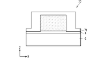
- the n-type SiC layer 70 (second) so as to cover the peripheral portion of the convex portion 62 of the p-type SiC layer 60 and the peripheral portion of the n-type SiC layer 4 around the convex portion 62 by epitaxial growth. (Semiconductor layer) is formed.
- the surface of the n-type SiC layer 70 of the convex portion 62 of the p-type SiC layer 60 is flat, but may have irregularities.
- the crystal plane is formed by epitaxially growing the n-type SiC layer 70 in a state where the periphery of the convex portion 62 of the p-type SiC layer 60 is dug down until the surface of the n-type SiC layer 4 is exposed. Voids are not formed due to the difference in crystal growth rate due to the difference in orientation, and the ineffective region can be reduced. Therefore, processing for separating the void becomes unnecessary, and the manufacturing cost can be reduced.
- the concentration of n-type impurities in the n-type SiC layer 70 can be set so that the product of the impurity concentration of the p-type pillar 7p and the width substantially matches the product of the impurity concentration of the n-type pillar 7n and the width.
- the n-type SiC layer 70 on the convex portion 62 of the p-type SiC layer 60 is removed by polishing or dry etching to expose the upper surface of the convex portion 62.
- a part of the upper portion of the convex portion 62 of the p-type SiC layer 60 can be removed.
- the upper part of the n-type chip peripheral portion 71 of the n-type SiC layer 70 can be partially removed.
- FIG. 60 shows a perspective view of the silicon carbide semiconductor device 300 formed by the above method before the MOSFET cell region MCR and the MOSFET terminal region MTR are formed.
- the pillar portion 7 is a region in which a plurality of n-type pillars 7n having a striped plan view shape and a plurality of p-type pillars 7p are alternately arranged on the semiconductor substrate 3.
- the arrangement direction of is orthogonal to the direction in which the main current of the silicon carbide semiconductor device 300 flows.
- An n-type pillar peripheral portion 73 containing an n-type impurity is provided so as to surround the pillar portion 7, and the outer side of the n-type pillar peripheral portion 73 is an n-type chip peripheral portion 71 containing an n-type impurity.
- FIGS. 55 to 60 show a configuration in which the pillar portion 7 is provided with three p-type pillars 7p and four n-type pillars 7n, the number actually corresponds to the size of the carbonized semiconductor device.
- the p-type pillar 7p and the n-type pillar 7n are formed.
- FIG. 61 shows a cross-sectional view in the arrow direction along the AA line (line parallel to the Y axis) and a cross-sectional view in the arrow direction along the BB line (line parallel to the X axis) in FIG. 60.
- FIG. 61 is a cross-sectional view taken along the line AA in the process shown in FIG. 55.
- the cross-sectional view taken along the line BB is the same as that in FIG. 55.
- FIG. 62 is a cross-sectional view taken along the line AA in the process shown in FIG. 56.
- the cross-sectional view taken along the line BB is the same as that in FIG. 56.
- FIG. 63 is a cross-sectional view taken along the line AA in the process shown in FIG. 57
- FIG. 64 is a cross-sectional view taken along the line BB
- FIG. 65 is a cross-sectional view taken along the line AA in the process shown in FIG. 58
- FIG. 66 is a cross-sectional view taken along the line BB
- FIG. 67 is a cross-sectional view taken along the line AA in the process shown in FIG. 59
- FIG. 68 is a cross-sectional view taken along the line BB.
- the impurity concentration is increased in the n-type pillar peripheral portion 73 and the n-type pillar 7n.
- the product of the impurity concentration and the width of the n-type pillar peripheral portion 73 becomes larger than the product of the impurity concentration and the width of the n-type pillar 7n.
- the depletion layer does not spread over the entire n-type pillar peripheral portion 73, the electric field strength of the n-type pillar peripheral portion 73 is suppressed to a low level, and an increase in leakage current and a discharge risk are suppressed.
- the width of the peripheral portion 73 of the n-type pillar can be 1.2 times or more the width of the n-type pillar 7n.
- FIG. 69 is a perspective view of a silicon carbide semiconductor device 300 schematically showing a MOSFET cell region MCR when a MOSFET unit cell is provided in the pillar portion 7 and a MOSFET terminal region MTR provided on the outer periphery thereof.
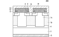
- FIG. 72 is a cross-sectional view corresponding to FIG. 67
- FIG. 71 shows an enlarged view of the region D in FIG. 70.
- the same components as those described with reference to FIG. 7 are designated by the same reference numerals, and duplicate description will be omitted.
- an n-type SiC layer 4 is provided on one main surface of the semiconductor substrate 3, and a plurality of p-type pillars 7p and a plurality of n-type pillars 7n alternate on the n-type SiC layer 4. It is provided in. Then, a plurality of p-type well regions 8 are selectively formed by ion implantation of p-type impurities from the upper layer portion of the p-type pillar 7p to the upper layer portion of the n-type pillar 7n. Further, in each well region 8, a p-type contact region 10 is formed by ion implantation of a p-type impurity so as to penetrate the well region 8.
- an n-type source region 9 is formed in the upper layer of the well region 8 by ion implantation of an n-type impurity so as to be in contact with both side surfaces of the contact region 10.
- activation annealing is performed to activate the implanted impurities.
- the thickness of the p-type well region 8 is, for example, 0.2 to 1.5 ⁇ m
- the concentration of the p-type impurity is, for example, 1 ⁇ 10 14 to 1 ⁇ 10 19 cm -3
- the thickness of the source region 9 is set.
- the concentration of n-type impurities is, for example, 1 ⁇ 10 17 to 1 ⁇ 10 21 cm -3
- the thickness of the contact region 10 is, for example, 0.2 to 1.5 ⁇ m.
- the concentration of the p-type impurity can be, for example, 1 ⁇ 10 18 to 1 ⁇ 10 21 m -3 .
- an insulating film used as a material for the gate insulating film 11, for example, a silicon oxide film 111 is formed on the pillar portion 7, and a conductor film serving as a gate electrode 12 is further formed on the silicon oxide film 111.
- a polysilicon film is formed.
- the polysilicon film is patterned to form the gate electrode 12 so as to straddle the upper edge portion of the adjacent source regions 9.
- an insulating film as a material of the interlayer insulating film 13 for example, a silicon oxide film 131 is formed so as to cover the gate electrode 12 and the silicon oxide film 111.
- the silicon oxide films 111 and 131 are patterned to form the interlayer insulating film 13 that covers the gate insulating film 11 and the gate electrode 12.
- a contact hole is formed which penetrates the interlayer insulating film 13 in the thickness direction and reaches a part of the source region 9 and the entire surface of the contact region 10.
- the inside of the contact hole is embedded and a conductor film is formed so as to cover the interlayer insulating film 13 to form the source electrode 14, and the other side of the semiconductor substrate 3 on the opposite side to the side where the source electrode 14 is provided.
- the drain electrode 15 on the main surface (back surface) of the silicon carbide semiconductor device 300, the silicon carbide semiconductor device 300 is completed.
- a plurality of p-type well regions 8 are selectively provided from the upper layer portion of the p-type pillar 7p to the upper layer portion of the n-type pillar 7n, and each well region 8 is provided.
- the configuration in which the p-type contact region 10 and the n-type source region 9 are provided is shown in the above, the p-type well region 8 and the like are not provided in the upper layer of the n-type pillar 7n and the p-type pillar 7p.
- n-type SiC layer 40 (third n-type SiC layer) is provided on the n-type pillars 7n and the p-type pillars 7p, and a p-type well region 8 or the like is provided in the n-type SiC layer 40.
- the manufacturing process will be described with reference to FIGS. 74 to 78 as another example of the method for manufacturing the semiconductor device.
- the n-type SiC layer 40 is grown by epitaxial growth so as to cover the region from the pillar portion 7 to the n-type chip peripheral portion 71 of the n-type SiC layer 70.
- the n-type SiC layer 40 can be formed on the entire surface of the semiconductor chip, can be formed only in the MOSFET cell region in which the MOSFET cell is formed, or can be formed in the MOSFET cell region and the MOSFET terminal region.
- FIG. 75 is a drawing showing an enlarged area of FIG. 74, and an enlarged view of the area E in FIG. 75 is shown in FIG. 76.
- FIG. 76 the same components as those described with reference to FIG. 7 are designated by the same reference numerals, and duplicate description will be omitted.
- a plurality of p-type well regions 8 are selectively formed in the n-type SiC layer 40 from above the p-type pillar 7p to above the n-type pillar 7n by ion implantation of p-type impurities. do.
- a p-type contact region 10 is formed by ion implantation of a p-type impurity so as to penetrate the well region 8.
- an n-type source region 9 is formed in the upper layer of the well region 8 by ion implantation of an n-type impurity so as to be in contact with both side surfaces of the contact region 10.
- activation annealing is performed to activate the implanted impurities.
- an insulating film used as a material for the gate insulating film 11, for example, a silicon oxide film 111 is formed on the n-type SiC layer 40, and further, a gate electrode 12 is formed on the silicon oxide film 111.
- a conductor film, for example a polysilicon film, is formed.
- the polysilicon film is patterned to form the gate electrode 12 so as to straddle the upper edge portion of the adjacent source regions 9.
- an insulating film as a material of the interlayer insulating film 13, for example, a silicon oxide film 131 is formed so as to cover the gate electrode 12 and the silicon oxide film 111.
- the silicon oxide films 111 and 131 are patterned to form the interlayer insulating film 13 that covers the gate insulating film 11 and the gate electrode 12.
- a contact hole is formed which penetrates the interlayer insulating film 13 in the thickness direction and reaches a part of the source region 9 and the entire surface of the contact region 10.
- the inside of the contact hole is embedded and a conductor film is formed so as to cover the interlayer insulating film 13 to form the source electrode 14, and the other side of the semiconductor substrate 3 on the opposite side to the side where the source electrode 14 is provided.
- the drain electrode 15 on the main surface (back surface) of the silicon carbide semiconductor device 300A, the silicon carbide semiconductor device 300A is completed.
- voids are not formed when the n-type pillar 7n is formed by epitaxial growth, and the ineffective region can be reduced. Therefore, processing for separating the void becomes unnecessary, and the manufacturing cost can be reduced.
- FIGS. 73 and 78 a configuration in which two MOSFET unit cells are provided is shown, but in reality, a number of unit cells are formed according to the size of the carbonized semiconductor device.
- FIGS. 79 and 80 are views corresponding to FIGS. 65 and 66, respectively.
- the convex portion 62 of the p-type SiC layer 60 is formed, the surface of the peripheral portion of the n-type SiC layer 4 is exposed, and then the p-type SiC layer 60 is subjected to epitaxial growth.
- the n-type SiC layer 70 is formed so as to cover the peripheral portion of the convex portion 62 and the peripheral portion of the n-type SiC layer 4 around the convex portion 62, the n-type SiC layer 70 is formed as shown in FIGS. 79 and 80.
- the width 73W of the n-type pillar peripheral portion 73 is formed to be significantly larger than the width 7nW of the n-type pillar 7n.
- the product of the impurity concentration and the width of the n-type pillar peripheral portion 73 is larger than the product of the impurity concentration and the width of the n-type pillar 7n. It will be significantly larger. With such a configuration, the depletion layer does not spread over the entire n-type pillar peripheral portion 73, the electric field strength of the n-type pillar peripheral portion 73 is suppressed to a low level, and an increase in leakage current and a discharge risk are suppressed.
- FIGS. 81 and 82 are views corresponding to FIGS. 65 and 66, respectively.
- the convex portion 62 of the p-type SiC layer 60 is formed, the surface of the peripheral portion of the n-type SiC layer 4 is exposed, and then the p-type SiC layer 60 is subjected to epitaxial growth.
- the n-type SiC layer 70 is formed so as to cover the peripheral portion of the convex portion 62 and the peripheral portion of the n-type SiC layer 4 around the convex portion 62, as shown in FIGS. 81 and 82, the peripheral portion 73 of the n-type pillar.
- the n-type impurity concentration of the n-type pillar 7n is formed to be higher than the n-type impurity concentration of the n-type pillar 7n.
- the epitaxial conditions of the n-type SiC layer 70 are adjusted so that the n-type pillar peripheral portion 73 can easily take in n-type impurities than between the convex portions 62 of the p-type SiC layer 60.
- the n-type pillar peripheral portion 73 is substantially limited to crystal growth from the bottom surface of the trench, but the amount of impurities taken up differs between the convex portions 62 because the crystals grow from the plurality of surfaces of the bottom surface of the trench and the side wall of the trench. Further, since the ease of supplying the raw material gas and the impurity gas differs between the n-type pillar peripheral portion 73 dug down in a wide area and the convex portion 62 dug down in a narrow width, these factors are used. The epitaxial conditions of the n-type SiC layer 70 are adjusted in consideration.
- the product of the impurity concentration and the width of the n-type pillar peripheral portion 73 is the impurity concentration and width of the n-type pillar 7n. Is greater than the product of.
- the product of the impurity concentration and the width of the n-type pillar peripheral portion 73 is calculated from the product of the impurity concentration and the width of the n-type pillar 7n. Can also be made significantly larger. With such a configuration, the depletion layer does not spread over the entire n-type pillar peripheral portion 73, the electric field strength of the n-type pillar peripheral portion 73 is suppressed to a low level, and an increase in leakage current and a discharge risk are suppressed.
- FIGS. 83 and 84 are views corresponding to FIGS. 65 and 66, respectively.
- the convex portion 62 of the p-type SiC layer 60 is formed, the surface of the peripheral portion of the n-type SiC layer 4 is exposed, and then the p-type SiC layer 60 is subjected to epitaxial growth.
- the n-type SiC layer 70 is formed so as to cover the peripheral portion of the convex portion 62 and the peripheral portion of the n-type SiC layer 4 around the convex portion 62, as shown in FIGS.
- the n-type pillar peripheral portion 73 Ion injection of n-type impurities is performed so that the concentration of n-type impurities in the peripheral portion 73 of the n-type pillars is higher than the concentration of n-type impurities in the n-type pillars 7n.
- the product of the impurity concentration and the width of the n-type pillar peripheral portion 73 becomes larger than the product of the impurity concentration and the width of the n-type pillar 7n.
- the depletion layer does not spread over the entire n-type pillar peripheral portion 73, the electric field strength of the n-type pillar peripheral portion 73 is suppressed to a low level, and an increase in leakage current and a discharge risk are suppressed.
- ion implantation into the n-type pillar peripheral portion 73 can be performed only at necessary locations.
- the epitaxial growth rate and the epitaxial concentration may differ depending on the crystal orientation.
- the product of the impurity concentration and the width of the n-type pillar peripheral portion 736 may not be uniformly formed, and the product of the impurity concentration and the width of the n-type pillar peripheral portion 73 may be formed.
- a location smaller than the product of the impurity concentration and width of the n-type pillar 7n may be formed.
- ion injection is performed only in the portion where the product of the concentration and width of the n-type pillar peripheral portion 73 is smaller than the product of the impurity concentration and width of the n-type pillar peripheral portion 73, and the concentration and width of the n-type pillar peripheral portion 73 are The product can be larger than the product of the impurity concentration and the width of the n-type pillar peripheral portion 73.
- the semiconductor device has the same structure and size, a place where the product of the impurity concentration and the width of the n-type pillar peripheral portion 73 is smaller than the product of the impurity concentration and the width of the n-type pillar 7n always occurs in the same place. Therefore, it can be specified by making a sample, disassembling it, and verifying it.
- the reason why the product of the impurity concentration and the width of the n-type pillar peripheral portion 73 is smaller than the product of the impurity concentration and the width of the n-type pillar 7n is that the width of the n-type pillar peripheral portion 73 is narrow depending on the epitaxial condition. It is conceivable that the amount of n-type impurities taken up by the crystal plane is small and the concentration of n-type impurities is low.
- FIG. 85 is a diagram corresponding to FIG. 67.
- n-type SiC layer 70 on the convex portion 62 of the p-type SiC layer 600 is removed by polishing or dry etching to expose the upper surface of the convex portion 62.
- the n-type chip peripheral portion 71 outside the n-type pillar peripheral portion 73 is removed.
- the n-type chip peripheral portion 71 can be removed at the same time as the n-type SiC layer 70 on the convex portion 62 of the n-type SiC layer 70 by full surface etching, and the manufacturing process can be simplified. At this time, a part of the peripheral portion of the n-type SiC layer 4 can also be removed.
- FIGS. 86 and 87 are views corresponding to FIGS. 63 and 64, respectively.
- the p-type SiC layer 60 is etched by dry etching to form the convex portion 62 of the p-type SiC layer 60, and the p-type SiC layer 60 around the convex portion 62 is removed.
- the surface of the peripheral portion of the n-type SiC layer 4 is exposed, a part of the n-type SiC layer 4 is removed so as to form irregularities on the surface of the n-type SiC layer 4.
- the height 4H2 of the peripheral portion of the pillar of the type SiC layer 4 is lower than the height 4H1 of the n-type SiC layer 4 in the pillar portion 7.
- the main current of the MOSFET is less likely to flow in the peripheral portion of the chip, and as the main current in the MOSFET.
- the current withstand capacity increases when a large current flows.
- FIGS. 88 and 89 correspond to a cross-sectional view showing adjacent silicon carbide semiconductor devices 300 in a wafer state
- FIG. 88 is a cross-sectional view taken along the line AA of FIG. 69
- FIG. 892 is a cross-sectional view.
- the silicon carbide semiconductor device 300 is in the state shown in FIG. 73, the source electrode 14, the drain electrode 15, and the like are omitted.
- dicing is performed at the position indicated by the arrow between the two silicon carbide semiconductor devices 300 to separate them into chip units.
- the distance between the convex portions 62 of the p-type SiC layer 60 is compared with the pillar width of 0.5 to 5 ⁇ m of the n-type pillar 7n and the p-type pillar 7p. It is 10 times or more, for example, 50 ⁇ m or more.
- FIGS. 90 and 91 show the convex portion 62 of the p-type SiC layer 60 in the process shown in FIG. 63, and FIGS. 90 and 91 correspond to FIGS. 88 and 89, respectively.
- d1 the distance between the convex portions 62 in the adjacent silicon carbide semiconductor devices
- d2 the distance between the convex portions 62 in the adjacent silicon carbide semiconductor devices
- the silicon carbide semiconductor device in which the MOSFET cell region and the MOSFET terminal region are formed in the pillar portion 7 is shown, but the application of the present disclosure is not limited to the MOSFET.
- a silicon carbide semiconductor device having an SBD region and an SBD terminal region formed in the pillar portion 7 may be used, and an IGBT (Insulated Gate Bipolar Transistor cell region) and an IGBT terminal region may be formed in the pillar portion 7 to form a silicon carbide semiconductor device. You can also.
- the device is not limited to a transistor, and a silicon carbide semiconductor device in which a pn diode region and a pn diode termination region are formed in a pillar portion 7 can be used, and the same effect can be obtained if it is a vertical power device.
- the application to the silicon carbide semiconductor device is exemplified, but the present disclosure can also be applied to the silicon (silicon) semiconductor device.
- FIG. 92 is a cross-sectional perspective view schematically showing the unit cell configuration of the MOSFET 101.
- FIG. 93 is a partially enlarged view of the source electrode 31 in FIG. 92 in which the illustration is omitted.
- FIG. 94 is a diagram omitting the illustration of the structure in the vicinity of the gate electrode 29 in FIG. 93.
- the MOSFET 101 includes an n-type semiconductor substrate 21, a drain electrode 32, a super junction layer 90, a plurality of p-type well regions 25a, and a plurality of n-type source regions 26a. It has a plurality of p-type well regions 25b, a plurality of n-type source regions 26b, a gate electrode 29, and a source electrode 31.
- the MOSFET 101 has a gate insulating film 28, a gate electrode 29, and an interlayer insulating film 30 in order to form a MOS structure.
- the MOSFET 101 has an epitaxial layer 22.
- the MOSFET 101 has a p-type contact region 27a and a p-type contact region 27b.
- the semiconductor substrate 21 has a lower surface S1 and an upper surface S2 opposite to the lower surface S1.
- the XYZ coordinate system shown in the figure is arranged so that the XY plane is parallel to the upper surface S2 and the Z axis is parallel to the thickness direction of the semiconductor substrate 21.
- the current path of the MOSFET 101 is formed so as to connect the lower surface S1 and the upper surface S2. Therefore, the MOSFET 101 is a so-called vertical switching device.
- the epitaxial layer 22 is a layer formed by epitaxial growth on the upper surface S2 of the semiconductor substrate 21.
- the epitaxial layer 22 has an n-type.
- the impurity concentration of the epitaxial layer 22 is lower than the impurity concentration of the semiconductor substrate 21.
- the super junction layer 90 is provided on the upper surface S2 of the semiconductor substrate 21 via the epitaxial layer 22.
- the super junction layer 90 has a plurality of n-type pillars 23 and a plurality of p-type pillars 24 alternately in the in-plane direction (XY in-plane direction) of the upper surface S2.
- the n-type pillars 23 and the p-type pillars 24 are alternately arranged in the X direction in the in-plane direction (XY in-plane direction), and the one in the in-plane direction (XY in-plane direction in FIG. 1).
- Each of the n-type pillar 23 and the p-type pillar 24 extends along a direction (Y direction) orthogonal to the direction (X direction). That is, in the layout parallel to the upper surface S2 of the semiconductor substrate 21, the n-type pillars 23 and the p-type pillars 24 are arranged in a stripe shape.
- the semiconductor substrate 21, the epitaxial layer 22, and the super junction layer 90 are made of SiC.
- the p-type well region 25a is provided in the upper layer of each of the p-type pillars 24.
- the well region 25a extends on the super junction layer 90 so as to reach the n-type pillar 23.
- the n-type source region 26a is provided in the upper layer of each of the well regions 25a, and is separated from the n-type pillar 23 by the well region 25a.
- the p-type well region 25b is provided in the upper layer of each of the n-type pillars 23.
- the well region 25b is arranged away from the p-type pillar 24.
- the n-type source region 26b is provided in the upper layer of each of the well regions 25b, and is separated from the n-type pillar 23 by the well region 25b.
- the well region 25a and the well region 25b are arranged in a stripe shape. Further, the width of each of the well regions 25b is smaller than the width of each of the well regions 25a. The width of each of the well regions 25a may be the same, and the width of each of the well regions 25b may be the same.
- the source electrode 31 is provided on the upper surface S2 side of the semiconductor substrate 21, and is bonded to each of the well region 25a, the well region 25b, the source region 26a, and the source region 26b.
- the gate electrode 29 faces the well region 25a between the n-type pillar 23 and the source region 26a and faces the well region 25b between the n-type pillar 23 and the source region 26b via the gate insulating film 28. There is.
- the gate electrode 29 has a striped planar layout, as shown in FIG. 93.
- the interlayer insulating film 30 insulates between the gate electrode 29 and the source electrode 31.
- an n-type epitaxial layer 54 is provided on one main surface of an n-type semiconductor substrate 53 made of silicon carbide, and a p-type epitaxial layer 54 is provided on the upper layer of the epitaxial layer 54.
- a plurality of well regions 57 are selectively provided, and a p-type contact region 60a is provided in each well region 57 so as to penetrate the well region 57.
- An n-type source region 58 is provided in the upper layer of the well region 57 in contact with both side surfaces of the contact region 60a.
- the thickness of the source region 58 is thinner than the thickness of the well region 57, and the thickness of the contact region 60a is set to be about the same as the thickness of the well region 57, or the contact region 60a is provided to be slightly deeper.
- the gate insulating film 61 is selectively formed on the epitaxial layer 54, and the gate electrode 63 is formed on the gate insulating film 61. That is, the gate insulating film 61 extends from the upper part of the source region 58 to the upper part of the well region 57 and the epitaxial layer 54 to the upper part of the source region 58 of the adjacent well regions 57 between the adjacent source regions 58.
- the gate electrode 63 is provided so as to cover the gate insulating film 61.
- the interlayer insulating film 64 is formed so as to cover the gate insulating film 61 and the gate electrode 63, and the source electrode 65 is formed so as to cover the interlayer insulating film 64.
- the interlayer insulating film 64 includes a contact hole SC that penetrates the interlayer insulating film 64 in the thickness direction and reaches a part of the source region 58 and the entire surface of the contact region 60a in a region other than the region covering the gate electrode 63. It is provided.
- the contact hole SC is filled with the source electrode 65, and the source electrode 65 is connected to the source region 58 and the contact region 60a.
- a plurality of MOSFETs composed of the source region 58 and the like are arranged in a horizontal direction with respect to the main surface of the semiconductor substrate 53 and connected in parallel to form an element group.
- the region where this element group is provided is defined as an element region (active region) ER, and a terminal region TR that realizes the withstand voltage of the MOSFET 102 is provided on the outer peripheral portion of the element region ER.
- the element region ER corresponds to the MOSFET cell region MCR
- the termination region TR corresponds to the MOSFET termination region MTR.
- a p-type contact region 60b is provided in the upper layer of the epitaxial layer 54 in the terminal region TR so as to define the outer edge of the element region ER.
- the contact region 60b is provided so as to have the same thickness as the contact region 60a, but its width is wider than that of the contact region 60a.
- a p-type Resurf region 69 is provided outside the contact region 60b so as to have the same thickness as the contact region 60b.
- a plurality of n-type pillar layers 55a and p-type pillar layers 56a are provided alternately in the element region ER so that their respective numbers are evenly arranged, and a terminal region thereof is provided.
- a plurality of n-type pillar layers 55b and p-type pillar layers 56b are alternately arranged and provided in the formation region of the contact region 60b and the resurf region 69.
- a plurality of n-type pillar layers 55a and the p-type pillar layer 56a are alternately arranged and provided.
- Each pillar layer is provided so as to extend from the outermost surface of the epitaxial layer 54 toward the semiconductor substrate 53 in the depth direction of the epitaxial layer 54, and the deepest portion thereof is set to be shallower than the thickness of the epitaxial layer 54. Will be done.
- the widths of the n-type pillar layer 55a and the p-type pillar layer 56a are the same, and the total value of both is the pillar pitch W1. Further, the widths of the n-type pillar layer 55b and the p-type pillar layer 56b are also the same, but the respective widths are set wider than the respective widths of the n-type pillar layer 55a and the p-type pillar layer 56a, and are n-type.
- the field insulating film 81 is provided on the epitaxial layer 54, and the interlayer insulating film 64 is provided on the field insulating film 81.
- the source electrode 65 is provided so as to extend from the element region ER to the laminated film of the field insulating film 81 and the interlayer insulating film 64 in the terminal region TR.
- the laminated film of the field insulating film 81 and the interlayer insulating film 64 is provided with a contact hole TC in a region corresponding to the upper portion of the contact region 60b, which penetrates the laminated film in the thickness direction and reaches the contact region 60b. ing.
- the contact hole TC is filled with the source electrode 65, and the source electrode 65 is connected to the contact region 60b.
- the laminated film of the field insulating film 81 and the interlayer insulating film 64 is provided so as to cover a part of the upper part of the MOSFET on the outermost periphery of the element region ER, and also a part of the upper part of the source electrode 65 and the field insulating film 81.
- a passivation film 87 is provided so as to cover the upper part of the laminated film of the interlayer insulating film 64 and the interlayer insulating film 64.
- drain electrode 86 is provided on the other main surface (back surface) of the semiconductor substrate 53 on the side opposite to the side where the source electrode 65 is provided.
- FIG. 96 After forming the n-type pillar layers 55a and 55b and the p-type pillar layers 56a and 56b, that is, after undergoing the manufacturing process described with reference to FIGS. 13 to 17, for example, by photoengraving. Ion implantation of impurities was performed using a patterned resist mask (not shown), and well regions 57, source regions 58, resurf regions 59, contact regions 60a and 60b were selectively provided in the upper layer of the epitaxial layer 54. Form.
- p-type impurities are introduced into the well region 57, the resurf region 59, the contact regions 60a and 60b, and the n-type impurities are introduced into the source region 58.
- the contact regions 60a and 60b can be ion-implanted using the same resist mask, and the impurity concentration can be in the range of 1 ⁇ 10 18 to 1 ⁇ 10 21 cm -3.
- the impurity concentrations in the well region 57 and the resurf region 59 can be in the range of 1 ⁇ 10 15 to 1 ⁇ 10 19 cm -3 , and the depth can be in the range of, for example, 0.3 to 4.0 ⁇ m. ..
- the impurity concentration of the source region 58 can be in a range exceeding the impurity concentration of the well region 57, for example, in the range of 1 ⁇ 10 18 to 1 ⁇ 10 21 cm -3 . Further, the depth of the source region 58 is set to a depth that does not exceed the well region 57.
- the contact regions 60a and 60b can be ion-implanted using the same resist mask, and the impurity concentration can be in the range of 1 ⁇ 10 18 to 1 ⁇ 10 21 cm -3. Ion implantation can be performed at a substrate temperature of 200 ° C. or higher.
- the contact regions 60a and 60b are regions provided for achieving good metal contact with the well region 57 and the resurf region 59, and can operate as a semiconductor device without providing the contact regions 60a and 60b.
- heat treatment is performed in an inert gas such as argon or nitrogen or in a vacuum at a temperature of 1500 to 2200 ° C. for 0.5 to 60 minutes after the introduction of impurities.
- an inert gas such as argon or nitrogen or in a vacuum
- the injected impurities are electrically activated.
- an oxide film is formed by sacrificial oxidation on the epitaxial layer 54, and then the surface alteration layer of the epitaxial layer 54 is removed by removing the oxide film with hydrofluoric acid to obtain a clean surface.
- the well region 57 is formed so as to cover the upper layer portion of the p-type pillar layer 56a, and the p-type pillar layer 56a passes through the contact region 60a and the source electrode 55 (FIG. 95). ) And electrically connected.
- the contact region 60b and the resurf region 59 are formed so as to cover the upper layer portion over the upper layer portions of the plurality of p-type pillar layers 56b, respectively, and the plurality of p-types covered by the contact region 60b.
- the pillar layer 56b has the same potential via the contact region 60b, and the plurality of p-type pillar layers 56b covered with the resurf region 59 have the same potential via the resurf region 59. Since the contact region 60b and the resurf region 59 are provided so that the side surfaces of the contact region 60b are in contact with each other, the plurality of p-type pillar layers 56b covered with the contact region 60b are connected to the source electrode 55 (via the contact region 60b). It is electrically connected to FIG. 95).
- FIG. 97 is a plan view showing the surface structure of the semiconductor substrate 44 of the semiconductor device 103
- FIG. 98 is a cross-sectional view taken along the line A1-A2 of FIG. 97
- FIG. 99 is a B1 of FIG. 97.
- -It is a cross-sectional view in the direction indicated by the arrow on the B2 line.
- the semiconductor device 103 is formed by using a semiconductor substrate 44 made of n-type SiC having an off-angle.
- An n-type drift layer 41 is formed on the semiconductor substrate 44 by epitaxial growth.
- a plurality of p-type pillar regions 42 are formed in the drift layer 41. As shown in FIG. 97, each of the p-type pillar regions 42 has a plan view shape and is striped. Since a plurality of p-type pillar regions 42 are provided in the drift layer 41, the drift layer 41 sandwiched between the p-type pillar regions 42 becomes an n-type pillar region.
- a surface electrode 45 as an anode electrode of the SBD is formed on the drift layer 41 including the p-type pillar region 42. Further, a back surface electrode 46 as a cathode electrode of the SBD is formed on the lower surface of the semiconductor substrate 44.
- the front electrode 45 is shotkey connected to the drift layer 41 and the p-type pillar region 42, and the back electrode 46 is ohmic contacted to the semiconductor substrate 44.
- a plurality of frame-shaped pressure-resistant holding structures 43 which are p-type semiconductor regions, are concentrically formed so as to surround the surface electrode 45.
- the region surrounded by the withstand voltage holding structure 43 is the active region of the semiconductor device 103, and the formation region of the withstand voltage holding structure 43 and the outside thereof are the termination regions of the semiconductor device 103. In some cases, the end region is outside the active region, including the pressure resistance holding structure 43.
- each of the withstand voltage holding structures 43 includes a side extending parallel to the p-type pillar region 42 and a side orthogonal to the p-type pillar region 42 in a plan view.
- the plan view shape of the chip of the semiconductor device 103 is rectangular. Therefore, in the vicinity of the side parallel to the extending direction of the p-type pillar region 42 of the semiconductor device 103, each withstand voltage holding structure 43 extends parallel to the p-type pillar region 42 and is perpendicular to the extending direction of the p-type pillar region 42. In the vicinity of the parallel side, each withstand voltage holding structure 43 extends so as to be orthogonal to the p-type pillar region 42.
- At least one of the plurality of pressure-resistant holding structures 43 is formed so as to overlap a part of the surface electrode 45 in a plan view. More specifically, as shown in FIGS. 98 and 99, the innermost pressure-resistant structure 43 is formed so as to overlap the end portion of the surface electrode 45.
- each embodiment can be freely combined, and each embodiment can be appropriately modified or omitted.
- 3 semiconductor substrate 4 n-type SiC layer, 6 p-type pillar peripheral part, 7 pillar part, 7n n-type pillar, 7p p-type pillar, 5 p-type chip peripheral part, 60 p-type SiC layer, 70 n-type SiC layer, 71 n-type chip peripheral part, 72 convex part, 73 n-type pillar peripheral part.
Landscapes
- Insulated Gate Type Field-Effect Transistor (AREA)
- Chemical & Material Sciences (AREA)
- Composite Materials (AREA)
- Crystals, And After-Treatments Of Crystals (AREA)
- Electrodes Of Semiconductors (AREA)
- Recrystallisation Techniques (AREA)
Priority Applications (5)
| Application Number | Priority Date | Filing Date | Title |
|---|---|---|---|
| DE112020007344.0T DE112020007344T5 (de) | 2020-06-24 | 2020-06-24 | Halbleitereinheit und verfahren zur herstellung einer halbleitereinheit |
| US17/918,330 US12477789B2 (en) | 2020-06-24 | 2020-06-24 | Semiconductor device having a plurality of pillars and method of manufacturing the semiconductor device |
| JP2022531324A JP7275393B2 (ja) | 2020-06-24 | 2020-06-24 | 半導体装置およびその製造方法 |
| CN202080102138.6A CN116057712B (zh) | 2020-06-24 | 2020-06-24 | 半导体装置及其制造方法 |
| PCT/JP2020/024829 WO2021260851A1 (ja) | 2020-06-24 | 2020-06-24 | 半導体装置およびその製造方法 |
Applications Claiming Priority (1)
| Application Number | Priority Date | Filing Date | Title |
|---|---|---|---|
| PCT/JP2020/024829 WO2021260851A1 (ja) | 2020-06-24 | 2020-06-24 | 半導体装置およびその製造方法 |
Publications (1)
| Publication Number | Publication Date |
|---|---|
| WO2021260851A1 true WO2021260851A1 (ja) | 2021-12-30 |
Family
ID=79282113
Family Applications (1)
| Application Number | Title | Priority Date | Filing Date |
|---|---|---|---|
| PCT/JP2020/024829 Ceased WO2021260851A1 (ja) | 2020-06-24 | 2020-06-24 | 半導体装置およびその製造方法 |
Country Status (5)
| Country | Link |
|---|---|
| US (1) | US12477789B2 (https=) |
| JP (1) | JP7275393B2 (https=) |
| CN (1) | CN116057712B (https=) |
| DE (1) | DE112020007344T5 (https=) |
| WO (1) | WO2021260851A1 (https=) |
Cited By (1)
| Publication number | Priority date | Publication date | Assignee | Title |
|---|---|---|---|---|
| WO2024075391A1 (ja) * | 2022-10-06 | 2024-04-11 | ローム株式会社 | 窒化物半導体装置 |
Families Citing this family (2)
| Publication number | Priority date | Publication date | Assignee | Title |
|---|---|---|---|---|
| IT202000016279A1 (it) * | 2020-07-06 | 2022-01-06 | St Microelectronics Srl | Procedimento di fabbricazione di un dispositivo semiconduttore in carburo di silicio con migliorate caratteristiche |
| JP7728204B6 (ja) * | 2022-03-04 | 2025-09-19 | 株式会社東芝 | 半導体装置 |
Citations (5)
| Publication number | Priority date | Publication date | Assignee | Title |
|---|---|---|---|---|
| JP2011108906A (ja) * | 2009-11-19 | 2011-06-02 | Renesas Electronics Corp | 半導体装置および半導体装置の製造方法 |
| JP2011228490A (ja) * | 2010-04-20 | 2011-11-10 | Denso Corp | 縦型半導体素子を備えた半導体装置およびその製造方法 |
| JP2013503492A (ja) * | 2009-08-27 | 2013-01-31 | ビシェイ−シリコニクス | スーパージャンクショントレンチパワーmosfetデバイスの製造 |
| WO2019069416A1 (ja) * | 2017-10-05 | 2019-04-11 | 三菱電機株式会社 | 半導体装置 |
| WO2019160086A1 (ja) * | 2018-02-19 | 2019-08-22 | 国立研究開発法人産業技術総合研究所 | 半導体装置 |
Family Cites Families (10)
| Publication number | Priority date | Publication date | Assignee | Title |
|---|---|---|---|---|
| JP4940546B2 (ja) * | 2004-12-13 | 2012-05-30 | 株式会社デンソー | 半導体装置 |
| JP2008182054A (ja) * | 2007-01-25 | 2008-08-07 | Toshiba Corp | 半導体装置 |
| JP2009087998A (ja) * | 2007-09-27 | 2009-04-23 | Sanyo Electric Co Ltd | 半導体装置 |
| JP2010028018A (ja) | 2008-07-24 | 2010-02-04 | Fuji Electric Device Technology Co Ltd | 半導体ウエハおよび半導体装置と半導体装置の製造方法 |
| JP2010040973A (ja) * | 2008-08-08 | 2010-02-18 | Sony Corp | 半導体装置およびその製造方法 |
| JP2012019088A (ja) | 2010-07-08 | 2012-01-26 | Denso Corp | 縦型半導体素子を備えた半導体装置 |
| EP2736072B1 (en) * | 2011-07-22 | 2017-01-11 | Fuji Electric Co., Ltd. | Superjunction semiconductor device |
| JP5692145B2 (ja) * | 2012-04-17 | 2015-04-01 | 株式会社デンソー | 炭化珪素半導体装置の製造方法 |
| JP6740759B2 (ja) * | 2016-07-05 | 2020-08-19 | 株式会社デンソー | 炭化珪素半導体装置およびその製造方法 |
| JP2018206914A (ja) * | 2017-06-02 | 2018-12-27 | 株式会社東芝 | 半導体装置 |
-
2020
- 2020-06-24 WO PCT/JP2020/024829 patent/WO2021260851A1/ja not_active Ceased
- 2020-06-24 DE DE112020007344.0T patent/DE112020007344T5/de active Pending
- 2020-06-24 US US17/918,330 patent/US12477789B2/en active Active
- 2020-06-24 JP JP2022531324A patent/JP7275393B2/ja active Active
- 2020-06-24 CN CN202080102138.6A patent/CN116057712B/zh active Active
Patent Citations (5)
| Publication number | Priority date | Publication date | Assignee | Title |
|---|---|---|---|---|
| JP2013503492A (ja) * | 2009-08-27 | 2013-01-31 | ビシェイ−シリコニクス | スーパージャンクショントレンチパワーmosfetデバイスの製造 |
| JP2011108906A (ja) * | 2009-11-19 | 2011-06-02 | Renesas Electronics Corp | 半導体装置および半導体装置の製造方法 |
| JP2011228490A (ja) * | 2010-04-20 | 2011-11-10 | Denso Corp | 縦型半導体素子を備えた半導体装置およびその製造方法 |
| WO2019069416A1 (ja) * | 2017-10-05 | 2019-04-11 | 三菱電機株式会社 | 半導体装置 |
| WO2019160086A1 (ja) * | 2018-02-19 | 2019-08-22 | 国立研究開発法人産業技術総合研究所 | 半導体装置 |
Cited By (1)
| Publication number | Priority date | Publication date | Assignee | Title |
|---|---|---|---|---|
| WO2024075391A1 (ja) * | 2022-10-06 | 2024-04-11 | ローム株式会社 | 窒化物半導体装置 |
Also Published As
| Publication number | Publication date |
|---|---|
| CN116057712B (zh) | 2024-11-05 |
| DE112020007344T5 (de) | 2023-04-06 |
| CN116057712A (zh) | 2023-05-02 |
| JP7275393B2 (ja) | 2023-05-17 |
| US20230147932A1 (en) | 2023-05-11 |
| JPWO2021260851A1 (https=) | 2021-12-30 |
| US12477789B2 (en) | 2025-11-18 |
Similar Documents
| Publication | Publication Date | Title |
|---|---|---|
| US6844592B2 (en) | Semiconductor device with super junction region | |
| JP6759563B2 (ja) | 半導体装置および半導体装置の製造方法 | |
| JP5395309B2 (ja) | 半導体装置およびその製造方法 | |
| JP6801323B2 (ja) | 半導体装置および半導体装置の製造方法 | |
| JP7293750B2 (ja) | 超接合炭化珪素半導体装置および超接合炭化珪素半導体装置の製造方法 | |
| JP4744958B2 (ja) | 半導体素子及びその製造方法 | |
| JP6848316B2 (ja) | 半導体装置および半導体装置の製造方法 | |
| JP7643621B2 (ja) | 半導体装置 | |
| US10777678B2 (en) | Semiconductor device | |
| US10790353B2 (en) | Semiconductor device with superjunction and oxygen inserted Si-layers | |
| CN108028282A (zh) | 半导体装置和半导体装置的制造方法 | |
| JP6766512B2 (ja) | 半導体装置および半導体装置の製造方法 | |
| US20200044077A1 (en) | Mosfet device with shielding region and manufacturing method thereof | |
| JP2019102737A (ja) | 半導体装置及びその製造方法 | |
| US10418478B2 (en) | Semiconductor device | |
| US20220285483A1 (en) | Insulated gate semiconductor device | |
| US10651270B2 (en) | Semiconductor device having a trench structure | |
| JP2025515379A (ja) | 炭化ケイ素プレーナーmosfet素子及びその製造方法 | |
| JP2018082055A (ja) | 半導体装置および半導体装置の製造方法 | |
| JP7275393B2 (ja) | 半導体装置およびその製造方法 | |
| JP2024111301A (ja) | 炭化珪素半導体装置 | |
| JP2023000187A (ja) | 半導体装置とその製造方法 | |
| JP7074173B2 (ja) | 半導体装置および半導体装置の製造方法 | |
| US20230246101A1 (en) | Semiconductor device and method for manufacturing semiconductor device | |
| JP7106882B2 (ja) | 半導体装置および半導体装置の製造方法 |
Legal Events
| Date | Code | Title | Description |
|---|---|---|---|
| 121 | Ep: the epo has been informed by wipo that ep was designated in this application |
Ref document number: 20941938 Country of ref document: EP Kind code of ref document: A1 |
|
| ENP | Entry into the national phase |
Ref document number: 2022531324 Country of ref document: JP Kind code of ref document: A |
|
| 122 | Ep: pct application non-entry in european phase |
Ref document number: 20941938 Country of ref document: EP Kind code of ref document: A1 |
|
| WWG | Wipo information: grant in national office |
Ref document number: 17918330 Country of ref document: US |