WO2021241677A1 - 有機発光素子 - Google Patents
有機発光素子 Download PDFInfo
- Publication number
- WO2021241677A1 WO2021241677A1 PCT/JP2021/020163 JP2021020163W WO2021241677A1 WO 2021241677 A1 WO2021241677 A1 WO 2021241677A1 JP 2021020163 W JP2021020163 W JP 2021020163W WO 2021241677 A1 WO2021241677 A1 WO 2021241677A1
- Authority
- WO
- WIPO (PCT)
- Prior art keywords
- organic compound
- light emitting
- organic
- group
- conc
- Prior art date
- Legal status (The legal status is an assumption and is not a legal conclusion. Google has not performed a legal analysis and makes no representation as to the accuracy of the status listed.)
- Ceased
Links
Images

Classifications
-
- H—ELECTRICITY
- H10—SEMICONDUCTOR DEVICES; ELECTRIC SOLID-STATE DEVICES NOT OTHERWISE PROVIDED FOR
- H10K—ORGANIC ELECTRIC SOLID-STATE DEVICES
- H10K50/00—Organic light-emitting devices
- H10K50/10—OLEDs or polymer light-emitting diodes [PLED]
- H10K50/11—OLEDs or polymer light-emitting diodes [PLED] characterised by the electroluminescent [EL] layers
- H10K50/12—OLEDs or polymer light-emitting diodes [PLED] characterised by the electroluminescent [EL] layers comprising dopants
- H10K50/121—OLEDs or polymer light-emitting diodes [PLED] characterised by the electroluminescent [EL] layers comprising dopants for assisting energy transfer, e.g. sensitization
-
- C—CHEMISTRY; METALLURGY
- C07—ORGANIC CHEMISTRY
- C07D—HETEROCYCLIC COMPOUNDS
- C07D491/00—Heterocyclic compounds containing in the condensed ring system both one or more rings having oxygen atoms as the only ring hetero atoms and one or more rings having nitrogen atoms as the only ring hetero atoms, not provided for by groups C07D451/00 - C07D459/00, C07D463/00, C07D477/00 or C07D489/00
- C07D491/02—Heterocyclic compounds containing in the condensed ring system both one or more rings having oxygen atoms as the only ring hetero atoms and one or more rings having nitrogen atoms as the only ring hetero atoms, not provided for by groups C07D451/00 - C07D459/00, C07D463/00, C07D477/00 or C07D489/00 in which the condensed system contains two hetero rings
- C07D491/04—Ortho-condensed systems
- C07D491/044—Ortho-condensed systems with only one oxygen atom as ring hetero atom in the oxygen-containing ring
- C07D491/048—Ortho-condensed systems with only one oxygen atom as ring hetero atom in the oxygen-containing ring the oxygen-containing ring being five-membered
-
- C—CHEMISTRY; METALLURGY
- C07—ORGANIC CHEMISTRY
- C07D—HETEROCYCLIC COMPOUNDS
- C07D495/00—Heterocyclic compounds containing in the condensed system at least one hetero ring having sulfur atoms as the only ring hetero atoms
- C07D495/02—Heterocyclic compounds containing in the condensed system at least one hetero ring having sulfur atoms as the only ring hetero atoms in which the condensed system contains two hetero rings
- C07D495/04—Ortho-condensed systems
-
- C—CHEMISTRY; METALLURGY
- C09—DYES; PAINTS; POLISHES; NATURAL RESINS; ADHESIVES; COMPOSITIONS NOT OTHERWISE PROVIDED FOR; APPLICATIONS OF MATERIALS NOT OTHERWISE PROVIDED FOR
- C09K—MATERIALS FOR MISCELLANEOUS APPLICATIONS, NOT PROVIDED FOR ELSEWHERE
- C09K11/00—Luminescent, e.g. electroluminescent, chemiluminescent materials
- C09K11/02—Use of particular materials as binders, particle coatings or suspension media therefor
-
- C—CHEMISTRY; METALLURGY
- C09—DYES; PAINTS; POLISHES; NATURAL RESINS; ADHESIVES; COMPOSITIONS NOT OTHERWISE PROVIDED FOR; APPLICATIONS OF MATERIALS NOT OTHERWISE PROVIDED FOR
- C09K—MATERIALS FOR MISCELLANEOUS APPLICATIONS, NOT PROVIDED FOR ELSEWHERE
- C09K11/00—Luminescent, e.g. electroluminescent, chemiluminescent materials
- C09K11/06—Luminescent, e.g. electroluminescent, chemiluminescent materials containing organic luminescent materials
-
- H—ELECTRICITY
- H10—SEMICONDUCTOR DEVICES; ELECTRIC SOLID-STATE DEVICES NOT OTHERWISE PROVIDED FOR
- H10K—ORGANIC ELECTRIC SOLID-STATE DEVICES
- H10K50/00—Organic light-emitting devices
- H10K50/10—OLEDs or polymer light-emitting diodes [PLED]
- H10K50/11—OLEDs or polymer light-emitting diodes [PLED] characterised by the electroluminescent [EL] layers
-
- H—ELECTRICITY
- H10—SEMICONDUCTOR DEVICES; ELECTRIC SOLID-STATE DEVICES NOT OTHERWISE PROVIDED FOR
- H10K—ORGANIC ELECTRIC SOLID-STATE DEVICES
- H10K50/00—Organic light-emitting devices
- H10K50/401—Organic light-emitting molecular electronic devices
-
- H—ELECTRICITY
- H10—SEMICONDUCTOR DEVICES; ELECTRIC SOLID-STATE DEVICES NOT OTHERWISE PROVIDED FOR
- H10K—ORGANIC ELECTRIC SOLID-STATE DEVICES
- H10K85/00—Organic materials used in the body or electrodes of devices covered by this subclass
- H10K85/60—Organic compounds having low molecular weight
- H10K85/649—Aromatic compounds comprising a hetero atom
- H10K85/657—Polycyclic condensed heteroaromatic hydrocarbons
- H10K85/6572—Polycyclic condensed heteroaromatic hydrocarbons comprising only nitrogen in the heteroaromatic polycondensed ring system, e.g. phenanthroline or carbazole
-
- C—CHEMISTRY; METALLURGY
- C09—DYES; PAINTS; POLISHES; NATURAL RESINS; ADHESIVES; COMPOSITIONS NOT OTHERWISE PROVIDED FOR; APPLICATIONS OF MATERIALS NOT OTHERWISE PROVIDED FOR
- C09K—MATERIALS FOR MISCELLANEOUS APPLICATIONS, NOT PROVIDED FOR ELSEWHERE
- C09K2211/00—Chemical nature of organic luminescent or tenebrescent compounds
- C09K2211/10—Non-macromolecular compounds
- C09K2211/1003—Carbocyclic compounds
- C09K2211/1007—Non-condensed systems
-
- C—CHEMISTRY; METALLURGY
- C09—DYES; PAINTS; POLISHES; NATURAL RESINS; ADHESIVES; COMPOSITIONS NOT OTHERWISE PROVIDED FOR; APPLICATIONS OF MATERIALS NOT OTHERWISE PROVIDED FOR
- C09K—MATERIALS FOR MISCELLANEOUS APPLICATIONS, NOT PROVIDED FOR ELSEWHERE
- C09K2211/00—Chemical nature of organic luminescent or tenebrescent compounds
- C09K2211/10—Non-macromolecular compounds
- C09K2211/1018—Heterocyclic compounds
-
- H—ELECTRICITY
- H10—SEMICONDUCTOR DEVICES; ELECTRIC SOLID-STATE DEVICES NOT OTHERWISE PROVIDED FOR
- H10K—ORGANIC ELECTRIC SOLID-STATE DEVICES
- H10K2101/00—Properties of the organic materials covered by group H10K85/00
- H10K2101/10—Triplet emission
-
- H—ELECTRICITY
- H10—SEMICONDUCTOR DEVICES; ELECTRIC SOLID-STATE DEVICES NOT OTHERWISE PROVIDED FOR
- H10K—ORGANIC ELECTRIC SOLID-STATE DEVICES
- H10K2101/00—Properties of the organic materials covered by group H10K85/00
- H10K2101/20—Delayed fluorescence emission
-
- H—ELECTRICITY
- H10—SEMICONDUCTOR DEVICES; ELECTRIC SOLID-STATE DEVICES NOT OTHERWISE PROVIDED FOR
- H10K—ORGANIC ELECTRIC SOLID-STATE DEVICES
- H10K2101/00—Properties of the organic materials covered by group H10K85/00
- H10K2101/30—Highest occupied molecular orbital [HOMO], lowest unoccupied molecular orbital [LUMO] or Fermi energy values
-
- H—ELECTRICITY
- H10—SEMICONDUCTOR DEVICES; ELECTRIC SOLID-STATE DEVICES NOT OTHERWISE PROVIDED FOR
- H10K—ORGANIC ELECTRIC SOLID-STATE DEVICES
- H10K2101/00—Properties of the organic materials covered by group H10K85/00
- H10K2101/90—Multiple hosts in the emissive layer
-
- H—ELECTRICITY
- H10—SEMICONDUCTOR DEVICES; ELECTRIC SOLID-STATE DEVICES NOT OTHERWISE PROVIDED FOR
- H10K—ORGANIC ELECTRIC SOLID-STATE DEVICES
- H10K50/00—Organic light-emitting devices
- H10K50/10—OLEDs or polymer light-emitting diodes [PLED]
- H10K50/11—OLEDs or polymer light-emitting diodes [PLED] characterised by the electroluminescent [EL] layers
- H10K50/12—OLEDs or polymer light-emitting diodes [PLED] characterised by the electroluminescent [EL] layers comprising dopants
-
- H—ELECTRICITY
- H10—SEMICONDUCTOR DEVICES; ELECTRIC SOLID-STATE DEVICES NOT OTHERWISE PROVIDED FOR
- H10K—ORGANIC ELECTRIC SOLID-STATE DEVICES
- H10K85/00—Organic materials used in the body or electrodes of devices covered by this subclass
- H10K85/60—Organic compounds having low molecular weight
- H10K85/649—Aromatic compounds comprising a hetero atom
- H10K85/654—Aromatic compounds comprising a hetero atom comprising only nitrogen as heteroatom
-
- H—ELECTRICITY
- H10—SEMICONDUCTOR DEVICES; ELECTRIC SOLID-STATE DEVICES NOT OTHERWISE PROVIDED FOR
- H10K—ORGANIC ELECTRIC SOLID-STATE DEVICES
- H10K85/00—Organic materials used in the body or electrodes of devices covered by this subclass
- H10K85/60—Organic compounds having low molecular weight
- H10K85/658—Organoboranes
Definitions
- the present invention relates to an organic light emitting device using a delayed fluorescent material.
- organic light emitting elements such as organic electroluminescence elements (organic EL elements).
- organic electroluminescence elements organic electroluminescence elements
- various studies have been conducted to improve the luminous efficiency by newly developing and combining electron transport materials, hole transport materials, host materials, light emitting materials and the like constituting organic electroluminescence elements.
- the delayed fluorescent material is a compound that emits fluorescence when returning from the excited singlet state to the ground state after the inverse intersystem crossing from the excited triplet state to the excited singlet state occurs in the excited state. Fluorescence by such a pathway is called delayed fluorescence because it is observed later than fluorescence from the excited singlet state directly generated from the ground state (normal fluorescence).
- fluorescent fluorescence when a luminescent compound is excited by injection of a carrier, the probability of occurrence of the excited singlet state and the excited triplet state is statistically 25%: 75%, so that the excited singlet state directly generated is used. There is a limit to the improvement of light emission efficiency only by the fluorescence of.
- the delayed fluorescent material not only the excited singlet state but also the excited triplet state can be used for fluorescence emission by the path via the above-mentioned inverse intersystem crossing, so that it is higher than the ordinary delayed fluorescent material. Luminous efficiency will be obtained.
- a benzene derivative having a heteroaryl group such as a carbazolyl group or a diphenylamino group and at least two cyano groups has been proposed, and high light emission efficiency can be obtained with an organic EL element using the benzene derivative as a light emitting layer. It has been confirmed that this was the case (see Patent Document 1). Further, in Non-Patent Document 1, the carbazolyl dicyanobenzene derivative (4CzTPN) is a thermally active delayed fluorescent material, and the organic electroluminescence device using this carbazolyl dicyanobenzene derivative has a high internal EL quantum. It has been reported that efficiency has been achieved.
- Patent Document 1 Patent Document 2, Patent Document 2, and Non-Patent Document 1 report that high luminous efficiency was obtained in an organic electroluminescence device using a delayed fluorescent material.
- Patent Document 2 when the present inventors have produced an organic electroluminescence element according to the descriptions in Patent Document 1 and Patent Document 2, it has been found that it is difficult to secure a sufficient life. It was also found that it is difficult to realize light emission with high color purity at a short wavelength.
- the present inventors have made diligent studies for the purpose of realizing a long life and high color purity in an organic light emitting device using a delayed fluorescent material.
- the present inventors have achieved high color purity by adding a plurality of delayed fluorescent materials, host materials, and light emitting materials that satisfy specific conditions to the light emitting layer. We have found that long-life light emission can be achieved.
- the present invention has been proposed based on such findings, and specifically has the following configuration.
- An organic light emitting element having a light emitting layer containing a first organic compound, a second organic compound, a third organic compound, and a fourth organic compound satisfying the following conditions (a) to (e).
- the second organic compound and the third organic compound are delayed fluorescent materials having different structures from each other.
- An organic light emitting device, wherein the maximum component of light emission from the organic light emitting device is light emission from the fourth organic compound.
- ET1 (2) represents the lowest excited triplet energy of the second organic compound.
- ET1 (3) represents the lowest excited triplet energy of the third organic compound.
- Conc (1) represents the concentration of the first organic compound in the light emitting layer.
- Conc (2) represents the concentration of the second organic compound in the light emitting layer.
- Conc (3) represents the concentration of the third organic compound in the light emitting layer.
- [2] The organic light emitting device according to [1], which further satisfies the following condition (c1).
- ET1 (4) represents the lowest excited triplet energy of the fourth organic compound.
- [3] The organic light emitting device according to [1], which further satisfies the following condition (d1).
- the second organic compound is the difference Delta] E st in energy between the lowest excited triplet state of lowest excited singlet state and 77K is less than 0.3 eV, according to any one of [1] to [5] Organic light emitting element.
- the third organic compound, the difference Delta] E st in energy between the lowest excited triplet state of lowest excited singlet state and 77K is less than 0.3 eV, according to any one of [1] to [6] Organic light emitting element.
- the first organic compound, the second organic compound, and the third organic compound are compounds each independently composed of an atom selected from the group consisting of a carbon atom, a hydrogen atom, and a nitrogen atom [1]. ] To [8].
- the organic light emitting device of the present invention can realize long-life light emission with high color purity.
- the description of the constituent elements described below may be based on typical embodiments and specific examples of the present invention, but the present invention is not limited to such embodiments and specific examples.
- the numerical range represented by using "-" in the present application means a range including the numerical values before and after "-" as the lower limit value and the upper limit value.
- “consisting of” means that it consists only of those described before “consisting of” and does not include anything else.
- the isotope species of hydrogen atoms existing in the molecule of the compound used in the present invention are not particularly limited, and for example, all the hydrogen atoms in the molecule may be 1 H, or some or all of them may be 2 H. (Duterium D) may be used.
- the organic light emitting element of the present invention has a light emitting layer containing a first organic compound, a second organic compound, a third organic compound and a fourth organic compound. Of these, the second organic compound and the third organic compound are delayed fluorescent materials having different structures from each other. Then, these organic compounds satisfy the following conditions (a) to (e). Conditions (a) E S1 (1)> E S1 (2)> E S1 (4)> E S1 (3) Condition (b) E S1 (2) -E S1 (3) ⁇ 0.30eV Conditions (c) ET1 (1)> ET1 (2)> ET1 (3) Conditions (d) Conc (1)> Conc (2)> Conc (3) Condition (e) Conc (3) ⁇ 20% by weight
- ES1 (1) represents the lowest excited single term energy of the first organic compound
- ES1 (2) represents the lowest excited single term energy of the second organic compound
- ES1 (3) represents the above.
- the lowest excited single term energy of the third organic compound is represented
- ES1 (4) represents the lowest excited single term energy of the fourth organic compound.
- eV is adopted as a unit.
- ET1 (1) represents the lowest excited triplet energy of the first organic compound
- ET1 (2) represents the lowest excited triplet energy of the second organic compound
- ET1 (3) represents the third organic.
- the lowest excited triplet energy of the compound is represented
- ET1 (4) represents the lowest excited triplet energy of the fourth organic compound.
- eV is adopted as a unit.
- Conc (1) represents the concentration of the first organic compound in the light emitting layer
- Conc (2) represents the concentration of the second organic compound in the light emitting layer
- Conc (3) represents the concentration of the third organic compound in the light emitting layer
- Conc (4) represents the concentration of the fourth organic compound in the light emitting layer.
- weight% is adopted as a unit.
- the organic light emitting device of the present invention simultaneously satisfies the condition (a) and the condition (b) for the lowest excited singlet energy. Therefore, the lowest excited singlet energies ES1 (2), ES1 (3), and ES1 (4) of the second organic compound, the third organic compound, and the fourth organic compound are all within the range of 0.3 eV. It is in. E S1 (2) -E S1 ( 3) may be or within the scope of the following 0.27 eV, or in the range of 0.24 eV, or to within the following ranges 0.20 eV.
- E S1 (4) may be closer to either E S1 (2) or E S1 (3), but for example, a compound closer to E S1 (2) than E S1 (3) can be selected.
- E S1 (2) -E S1 ( 4) and E S1 (4) -E S1 ( 3) are all or in 0.25eV within the range, or within the following ranges 0.20 eV, 0.15 eV It can be within the following range.
- E S1 (1) -E S1 ( 2) is or in the range of more than 0.2 eV, or in the range of more than 0.4 eV, can or in a range of more than 0.6 eV, also 1 It can be within the range of .5 eV or less, within the range of 1.2 eV or less, or within the range of 0.8 eV or less.
- the organic light emitting device of the present invention satisfies the relationship of the condition (c) with respect to the minimum excited triplet energy, but it is more preferable that the relationship of the following condition (c1) is also satisfied.
- E T1 (4) -E T1 ( 3) is or in the range of more than 0.01 eV, or in the range of more than 0.03 eV, can or in a range of more than 0.05 eV, also 0 It can be within the range of .3 eV or less, within the range of 0.2 eV or less, or within the range of 0.1 eV or less.
- E T1 (2) -E T1 ( 4) are or in the range of more than 0.01 eV, can or in a range of more than 0.05 eV, also or in the range of 0.3 eV, 0 It can be within the range of .2 eV or less.
- E T1 (1) -E T1 ( 2) is or in the range of more than 0.2 eV, can or in a range of more than 0.4 eV, also or in the range of 0.8 eV, 0 It can be within the range of .6 eV or less.
- the organic light emitting device of the present invention satisfies the relationship between the condition (d) and the condition (e) regarding the concentration of the organic compound in the light emitting layer. It is preferable that the organic light emitting device of the present invention further satisfies the following condition (d1).
- Conc (1) is preferably 30% by weight or more, can be in the range of 50% by weight or more, can be in the range of 65% by weight or more, and can be in the range of 99% by weight or less. , 85% by weight or less, or 75% by weight or less.
- Conc (2) is preferably 10% by weight or more, can be in the range of 20% by weight or more, can be in the range of 30% by weight or more, and can be in the range of 45% by weight or less. , 40% by weight or less, or 35% by weight or less.
- Conc (3) needs to be in the range of 20% by weight or less, preferably 15% by weight or less, and more preferably 10% by weight or less.
- Conc (3) may be in the range of 7% by weight or less, in the range of 0.5% by weight or more, in the range of 1.0% by weight or more, or in the range of 2% by weight or more. It can be in the range of 4% by weight or more.
- Conc (4) is preferably 5% by weight or less, and more preferably 3% by weight or less.
- Conc (4) can be in the range of 1% by weight or less, in the range of 0.5% by weight or less, in the range of 0.01% by weight or more, or in the range of 0.1% by weight. It can be within the above range or within the range of 0.3% by weight or more. It is preferable that the organic light emitting device of the present invention further satisfies the following condition (f).
- Conc (3) / Conc (4) can be in the range of 7 or more, in the range of 9 or more, in the range of 500 or less, in the range of 100 or less, or in the range of 50 or less. Can be within the range of.
- the second organic compound used in the organic light emitting device of the present invention is a delayed fluorescent material.
- the third organic compound is a delayed fluorescent material having a structure different from that of the second organic compound.
- the "delayed fluorescence material" in the present invention means that in an excited state, an intersystem crossing from an excited triplet state to an excited singlet state occurs, and fluorescence (delayed fluorescence) occurs when the excited singlet state returns to the ground state. It is an organic compound that emits light.
- the emission lifetime is measured by a fluorescence lifetime measurement system (such as a streak camera system manufactured by Hamamatsu Photonics)
- a material in which fluorescence with a emission lifetime of 100 ns (nanoseconds) or more is observed is referred to as a delayed fluorescence material.
- the second organic compound is preferably a difference Delta] E ST of the lowest excited triplet energy of the lowest excited singlet energy and 77K is less than 0.3 eV, more preferably less 0.25 eV, below 0.2eV It is more preferably 0.15 eV or less, further preferably 0.1 eV or less, even more preferably 0.07 eV or less, and further preferably 0.05 eV or less.
- Third organic compound is preferably a difference Delta] E ST of the lowest excited triplet energy of the lowest excited singlet energy and 77K is less than 0.3 eV, more preferably less 0.25 eV, below 0.2eV It is more preferably 0.15 eV or less, further preferably 0.1 eV or less, even more preferably 0.07 eV or less, and further preferably 0.05 eV or less. It is more preferably 0.03 eV or less, and particularly preferably 0.01 eV or less.
- the lowest excited singlet energy ( ES1 ) and the lowest excited triplet energy ( ET1 ) of the compound are the values obtained by the following procedure.
- Delta] E ST is a value determined by calculating the E S1 -E T1.
- Minimum excitation singlet energy ( ES1 ) A thin film of the compound to be measured or a toluene solution (concentration 10-5 mol / L) is prepared and used as a sample. The fluorescence spectrum of this sample is measured at room temperature (300K). In the fluorescence spectrum, the vertical axis is light emission and the horizontal axis is wavelength.
- the maximum point having a peak intensity of 10% or less of the maximum peak intensity of the spectrum is not included in the above-mentioned maximum value on the shortest wavelength side, and the value of the gradient closest to the maximum value on the shortest wavelength side is the maximum.
- the tangent line drawn at the point where the value is taken is taken as the tangent line to the rising edge of the phosphorescent spectrum on the short wavelength side.
- the first organic compound is an organic compound having a higher minimum excitation single term energy than the second organic compound, the third organic compound, and the fourth organic compound, and has a function as a host material responsible for carrier transport and a fourth organic compound. It has the function of confining energy in the compound.
- the fourth organic compound efficiently emits energy generated by the recombination of holes and electrons in the molecule and energy received from the first organic compound, the second organic compound, and the third organic compound. Can be converted to.
- the first organic compound is preferably an organic compound having a hole transporting ability and an electron transporting ability, preventing a long wavelength of light emission, and having a high glass transition temperature. Further, in a preferred embodiment of the present invention, the first organic compound is selected from compounds that do not emit delayed fluorescence. The following are preferable compounds that can be used as the first organic compound.
- the second organic compound is a delayed fluorescent material having a smaller minimum excitation singlet energy than the first organic compound and a larger minimum excitation singlet energy than the third organic compound and the fourth organic compound. Further, the second organic compound is a delayed fluorescent material having a lower minimum excited triplet energy than the first organic compound and a larger minimum excited triplet energy than the third organic compound.
- the second organic compound may be any compound that can emit delayed fluorescence under some conditions, and it is not essential for the organic light emitting device of the present invention to emit delayed fluorescence derived from the second organic compound. In the organic light emitting element of the present invention, the second organic compound receives energy from the first organic compound in the excited singlet state and transitions to the excited singlet state.
- the second organic compound may receive energy from the first organic compound in the excited triplet state and transition to the excited triplet state. Since the second organic compound is small Delta] E ST, second organic compound excited triplet state it is easy to reverse intersystem crossing to the second organic compound excited singlet state. The second organic compound in the excited singlet state generated by these paths gives energy to the third organic compound and the fourth organic compound to make these compounds transition to the excited singlet state.
- the following are preferable compounds that can be used as the second organic compound.
- t-Bu represents a tertiary butyl group.
- the third organic compound is a delayed fluorescent material having a lower minimum excited single term energy than the first organic compound, the second organic compound and the fourth organic compound, and has the lowest excited triple term than the first organic compound and the second organic compound. It is a delayed fluorescent material with low energy.
- the third organic compound may be any compound that can emit delayed fluorescence under some conditions, and it is not essential for the organic light emitting device of the present invention to emit delayed fluorescence derived from the third organic compound.
- the third organic compound plays a role of reducing the exciton burden of the second organic compound by transferring a part of the excitons generated by the second organic compound to the third organic compound. Fulfill.
- the concentration of the third organic compound in the light emitting layer of the organic light emitting element of the present invention is smaller than the concentration of the first organic compound and the concentration of the second organic compound, and is 20% by weight or less.
- the solution is used. Due to the chromic effect, the emission wavelength is shortened to a level at which energy can be transferred to the fourth compound. Thereby, the life of the organic light emitting device can be further extended and the desired chromaticity can be realized.
- the minimum excited triplet energy of the third organic compound is smaller than the minimum excited triplet energy of the fourth organic compound.
- the third organic compound receives energy from the fourth organic compound in the excited triplet state and transitions to the excited triplet state. Since the third organic compound has a small Delta] E ST, third organic compound excited triplet state is easy to reverse intersystem crossing to the third organic compound excited singlet state. The third organic compound in the excited singlet state generated by these paths can apply energy to the fourth organic compound to make the fourth organic compound transition to the excited singlet state.
- the following are preferable compounds that can be used as the third organic compound.
- Preferred delayed fluorescent materials include paragraphs 0008 to 0048 and 0995 to 0133 of WO2013 / 154064, paragraphs 0007 to 0047 and 0073 to 985 of WO2013 / 011954, and paragraphs 0007 to 0033 and 0059 to 0066 of WO2013 / 01955.
- WO 2013/081088 paragraphs 0008 to 0071 and 0118 to 0133, Japanese Patent Laid-Open No. 2013-256490, paragraphs 0009 to 0046 and 093 to 0134, Japanese Patent Laid-Open No.
- WO2014 / 136860 WO2014 / 196585, WO2014 / 189122, WO2014 / 168101, WO2015 / 008580, WO2014 / 203840, WO2015 / 002213, WO2015 / 016200, WO2015 / 019725, WO2015 / 072470, WO2015 / 108049, WO2015 / 080182, WO2015 / 072537, WO2015 / 080183, JP2015-129240, WO2015 / 129714, Described in WO2015 / 129715, WO2015 / 133501, WO2015 / 136880, WO2015 / 137244, WO2015 / 137202, WO2015 / 137136, WO2015 / 146541, WO2015 / 159541.
- a light emitting material that emits delayed fluorescence can be preferably adopted. It should be noted that the above publications described in this paragraph are cited here
- a compound represented by the following general formula (1) and emitting delayed fluorescence can be preferably used as the delayed fluorescent material of the present invention.
- a compound represented by the general formula (1) can be adopted as both the second organic compound and the third organic compound.
- X 1 to X 5 represent N or CR.
- R represents a hydrogen atom or a substituent.
- X 1 to X 5 represent CR, they may be the same or different from each other.
- at least one of X 1 to X 5 is CD (where D represents a donor group).
- Z represents an acceptor group
- at least one of X 1 to X 5 is N, Z represents a hydrogen atom or a substituent.
- a particularly preferable compound is a compound represented by the following general formula (2).
- X 1 to X 5 represent N or CR.
- R represents a hydrogen atom or a substituent.
- X 1 to X 5 may be the same or different from each other.
- at least one of X 1 to X 5 is CD (where D represents a donor group).
- the acceptor group represented by Z in the general formula (1) is a group having a property of donating an electron to the ring to which Z is bonded. Can be done.
- the donor group represented by D in the general formula (1) and the general formula (2) is a group having a property of attracting an electron to the ring to which D is bonded, for example, a group having a negative ⁇ p value of Hammett. You can choose from.
- the acceptor group may be referred to as A.
- the “hammet ⁇ p value” is L. P.
- the equilibrium constant of the benzene derivative substituted with, ⁇ represents the reaction constant determined by the type and conditions of the reaction.
- hammet ⁇ p value in the present invention and the numerical value of each substituent, refer to the description of the ⁇ p value in Hansch, C.et.al., Chem.Rev., 91,165-195 (1991). can.
- X 1 to X 5 represent N or CR, but at least one is CD.
- the number of N among X 1 to X 5 is 0 to 4, for example, X 1 and X 3 and X 5 , X 1 and X 3 , X 1 and X 4 , X 2 and X 3 , and X 1.
- X 5 , X 2 and X 4 , only X 1, only X 2, and only X 3 are N.
- the number of CDs is 1 to 5, preferably 2 to 5.
- At least one of X 1 to X 5 may be CA.
- A represents an acceptor group.
- the number of CAs is preferably 0 to 2, and more preferably 0 or 1.
- a cyano group is preferably mentioned as A of CA.
- X 1 to X 5 may be CD or CA independently.
- the two Rs may be coupled to each other to form a cyclic structure.
- the cyclic structure formed by bonding with each other may be an aromatic ring or an alicyclic ring, may contain a hetero atom, and the cyclic structure may be a fused ring having two or more rings. ..
- the hetero atom referred to here is preferably selected from the group consisting of a nitrogen atom, an oxygen atom and a sulfur atom.
- Examples of the cyclic structure formed include a benzene ring, a naphthalene ring, a pyridine ring, a pyridazine ring, a pyrimidine ring, a pyrazine ring, a pyrrol ring, an imidazole ring, a pyrazole ring, an imidazoline ring, an oxazole ring, an isooxazole ring, a thiazole ring, and an iso.
- Examples thereof include thiazole ring, cyclohexadiene ring, cyclohexene ring, cyclopentaene ring, cycloheptatriene ring, cycloheptadiene ring, cycloheptaene ring, furan ring, thiophene ring, naphthylidine ring, quinoxalin ring, quinoline ring and the like. ..
- a ring in which a large number of rings are condensed, such as triphenylene, may be formed.
- the donor group D in the general formula (1) and the general formula (2) is preferably a group represented by the following general formula (3), for example.
- R 11 and R 12 are independently substituted or unsubstituted alkyl groups, substituted or unsubstituted alkenyl groups, substituted or unsubstituted aryl groups, or substituted or unsubstituted heteroaryl groups, respectively.
- R 11 and R 12 may be combined with each other to form an annular structure.
- L represents a single bond, substituted or unsubstituted arylene group, or substituted or unsubstituted heteroarylene group.
- the substituent that can be introduced into the arylene group or heteroarylene group of L may be a group represented by the general formula (1) or the general formula (2), or may be a group represented by the general formula (1) to (6) described later.
- the groups represented by these (1) to (6) may be introduced up to the maximum number of substituents that can be introduced into L. Further, when a plurality of groups represented by the general formulas (1) to (6) are introduced, the substituents thereof may be the same or different from each other.
- * Represents the bond position to the carbon atom (C) constituting the ring skeleton of the ring in the general formula (1) or the general formula (2).
- the "alkyl group” referred to here may be linear, branched or cyclic. Further, two or more of the linear portion, the annular portion and the branched portion may be mixed. The number of carbon atoms of the alkyl group can be, for example, 1 or more, 2 or more, and 4 or more.
- the number of carbon atoms can be 30 or less, 20 or less, 10 or less, 6 or less, and 4 or less.
- Specific examples of the alkyl group include methyl group, ethyl group, n-propyl group, isopropyl group, n-butyl group, isobutyl group, tert-butyl group, n-pentyl group, isopentyl group, n-hexyl group and isohexyl group.
- 2-Ethylhexyl group, n-heptyl group, isoheptyl group, n-octyl group, isooctyl group, n-nonyl group, isononyl group, n-decanyl group, isodecanyl group, cyclopentyl group, cyclohexyl group, cycloheptyl group can be mentioned.
- the alkyl group as a substituent may be further substituted with an aryl group.
- the "alkenyl group" may be linear, branched or cyclic. Further, two or more of the linear portion, the annular portion and the branched portion may be mixed.
- the carbon number of the alkenyl group can be, for example, 2 or more and 4 or more. Further, the number of carbon atoms can be 30 or less, 20 or less, 10 or less, 6 or less, and 4 or less.
- Specific examples of the alkenyl group include ethenyl group, n-propenyl group, isopropenyl group, n-butenyl group, isobutenyl group, n-pentenyl group, isopentenyl group, n-hexenyl group, isohexenyl group and 2-ethylhexenyl group. Can be mentioned.
- the alkenyl group as a substituent may be further substituted with a substituent.
- the "aryl group” and the “heteroaryl group” may be a monocyclic ring or a condensed ring in which two or more rings are condensed.
- the number of fused rings is preferably 2 to 6, and can be selected from, for example, 2 to 4.
- the ring include a benzene ring, a pyridine ring, a pyrimidine ring, a triazine ring, a naphthalene ring, an anthracene ring, a phenanthrene ring, a triphenylene ring, a quinoline ring, a pyrazine ring, a quinoxaline ring, and a naphthylidine ring.
- arylene group or the heteroarylene group examples include a phenyl group, a 1-naphthyl group, a 2-naphthyl group, a 1-anthrasenyl group, a 2-anthrasenyl group, a 9-anthrasenyl group, a 2-pyridyl group, a 3-pyridyl group, and 4 -Pyridyl groups can be mentioned.
- Substituent means a monovalent group that can be substituted with a hydrogen atom, and is not a concept including those that condense.
- the description of the substituent and the preferable range of the general formula (7) described later can be referred to.
- the compound represented by the general formula (3) is preferably a compound represented by any of the following general formulas (4) to (6).
- R 51 to R 60 , R 61 to R 68 , and R 71 to R 78 each independently represent a hydrogen atom or a substituent.
- R 51 to R 60 , R 61 to R 68 , and R 71 to R 78 are groups represented by any of the above general formulas (4) to (6) independently.
- the number of substituents in the general formulas (4) to (6) is not particularly limited. It is also preferable that all are unsubstituted (that is, hydrogen atoms).
- the substituents may be the same or different.
- the substituent is preferably any one of R 52 to R 59 in the case of the general formula (4), and the general formula (5). If this is the case, it is preferably any of R 62 to R 67 , and if it is the general formula (6), it is preferably any of R 72 to R 77.
- X is a divalent oxygen atom having a chain length of 1 atom, a sulfur atom, a substituted or unsubstituted nitrogen atom, a substituted or unsubstituted carbon atom, a substituted or unsubstituted silicon atom, and a carbonyl.
- the description of the substituents in the above general formulas (1) and (2) can be referred to.
- L 12 to L 14 represent a single-bonded, substituted or unsubstituted arylene group, or a substituted or unsubstituted heteroarylene group.
- L 12 to L 14 are preferably single-bonded, substituted or unsubstituted arylene groups.
- the substituent of the arylene group or the heteroarylene group referred to here may be a group represented by the general formulas (1) to (6).
- the groups represented by the general formulas (1) to (6) may be introduced up to the maximum number of substituents that can be introduced into L 11 to L 14. Further, when a plurality of groups represented by the general formulas (1) to (6) are introduced, the substituents thereof may be the same or different from each other.
- * Represents the bond position to the carbon atom (C) constituting the ring skeleton of the ring in the general formula (1) or the general formula (2).
- a compound represented by the following general formula (7) and emitting delayed fluorescence can be particularly preferably used as a delayed fluorescent material.
- a compound represented by the general formula (7) can be adopted as both the second organic compound and the third organic compound.
- both the second organic compound and the third organic compound are compounds containing a dicyanobenzene structure.
- one 0-4 of R 1 ⁇ R 5 represents a cyano group, at least one of R 1 ⁇ R 5 represents a substituted amino group, the remaining R 1 ⁇ R 5 are a hydrogen atom, Alternatively, it represents a substituent other than a cyano group and a substituted amino group.
- the substituted amino group referred to here is preferably a substituted or unsubstituted diarylamino group, and the two aryl groups constituting the substituted or unsubstituted diarylamino group may be linked to each other.
- the linkage may be a single bond (in which case a carbazol ring is formed), -O-, -S-, -N (R 6 )-, -C (R 7 ) (R 8). )-, -Si (R 9 ) (R 10 )-may be made of a linking group.
- R 6 to R 10 represent hydrogen atoms or substituents
- R 7 and R 8 and R 9 and R 10 may be connected to each other to form a cyclic structure.
- the substituted amino group may be any of R 1 to R 5 , for example, R 1 and R 2 , R 1 and R 3 , R 1 and R 4 , R 1 and R 5 , R 2 and R 3 , R 2.
- R 3 and R 4 and R 5 can be substituted amino groups and the like.
- the cyano group may also be any of R 1 to R 5 , for example R 1 , R 2 , R 3 , R 1 and R 2 , R 1 and R 3 , R 1 and R 4 , R 1 and R 5 , R 2 and R 3 , R 2 and R 4 , R 1 and R 2 and R 3 , R 1 and R 2 and R 4 , R 1 and R 2 and R 5 , R 1 and R 3 and R 4 , R 1 And R 3 and R 5 , R 2 and R 3 and R 4 can be cyano groups and the like.
- R 1 to R 5 which are neither a cyano group nor a substituted amino group represent a hydrogen atom or a substituent.
- substituent examples include a hydroxyl group, a halogen atom (for example, a fluorine atom, a chlorine atom, a bromine atom, and an iodine atom), an alkyl group (for example, 1 to 40 carbon atoms), and an alkoxy group (for example, 1 to 40 carbon atoms).
- Alkylthio group for example, 1 to 40 carbon atoms
- aryl group for example, 6 to 30 carbon atoms
- aryloxy group for example, 6 to 30 carbon atoms
- arylthio group for example, 6 to 30 carbon atoms
- heteroaryl group for example, 6 to 30 carbon atoms.
- a ring skeleton constituent atom number 5 to 30 For example, a ring skeleton constituent atom number 5 to 30), a heteroaryloxy group (for example, a ring skeleton constituent atom number 5 to 30), a heteroarylthio group (for example, a ring skeleton constituent atom number 5 to 30), an acyl group (for example, a ring skeleton constituent atom number 1).
- alkenyl group eg carbon number 1-40
- alkynyl group eg carbon number 1-40
- alkoxycarbonyl group eg carbon number 1-40
- aryloxycarbonyl group eg carbon number 1-40
- Heteroaryloxycarbonyl groups eg, 1-40 carbon atoms
- silyl groups eg, trialkylsilyl groups with 1-40 carbon atoms
- nitro groups the groups listed here are further one or more groups listed here.
- a group of substituents A consisting of substituted groups can be mentioned.
- the substituent of the above-mentioned substituent group A can be mentioned, and further, a cyano group and a substituted amino group can also be mentioned.
- a compound represented by the following general formula (8) and emitting delayed fluorescence can also be particularly preferably used as the delayed fluorescent material of the present invention.
- a compound represented by the general formula (8) can be adopted as both the second organic compound and the third organic compound.
- Y 1 , Y 2 and Y 3 either represent a nitrogen atom and the remaining one represents a methine group, or all of Y 1 , Y 2 and Y 3 represent a nitrogen atom.
- Z 1 and Z 2 each independently represent a hydrogen atom or substituent.
- R 11 to R 18 each independently represent a hydrogen atom or a substituent , and at least one of R 11 to R 18 may be a substituted or unsubstituted arylamino group or a substituted or unsubstituted carbazolyl group. preferable.
- the benzene ring constituting the arylamino group and the benzene ring constituting the carbazolyl group may be combined with R 11 to R 18 , respectively to form a single bond or a linking group.
- the compound represented by the general formula (8) contains at least two carbazole structures in the molecule.
- the substituents that Z 1 and Z 2 can take include the above-mentioned substituents of the substituent group A.
- Specific examples of the substituents that can be taken from R 11 to R 18 , the above-mentioned arylamino group and carbazolyl group include the above-mentioned substituent, cyano group, substituted arylamino group and substituted alkylamino group of the substituent group A.
- R 11 and R 12 , R 12 and R 13 , R 13 and R 14 , R 15 and R 16 , R 16 and R 17 , and R 17 and R 18 are coupled to each other to form an annular structure. May be good.
- the compound represented by the general formula (9) is particularly useful.
- Y 1 , Y 2 and Y 3 either represent a nitrogen atom and the remaining one represents a methine group, or all of Y 1 , Y 2 and Y 3 represent a nitrogen atom.
- Z 2 represents a hydrogen atom or a substituent.
- R 11 to R 18 and R 21 to R 28 each independently represent a hydrogen atom or a substituent. At least one of R 11 to R 18 and / or at least one of R 21 to R 28 preferably represent a substituted or unsubstituted arylamino group or a substituted or unsubstituted carbazolyl group.
- the benzene ring constituting the arylamino group and the benzene ring constituting the carbazolyl group may be combined with R 11 to R 18 or R 21 to R 28 to form a single bond or a linking group, respectively.
- substituents that Z 2 can take include the above-mentioned substituents of the substituent group A.
- substituents that can be taken by R 11 to R 18 , R 21 to R 28 , the above arylamino group and the carbazolyl group the substituent, the cyano group and the substituted arylamino group of the above-mentioned substituent group A are described.
- Substituted alkylamino groups can be mentioned.
- R 11 and R 12 , R 12 and R 13 , R 13 and R 14 , R 15 and R 16 , R 16 and R 17 , R 17 and R 18 , R 21 and R 22 , R 22 and R 23 , R 23 and R 24 , R 25 and R 26 , R 26 and R 27 , and R 27 and R 28 may be coupled to each other to form an annular structure.
- R 11 and R 12 , R 12 and R 13 , R 13 and R 14 , R 15 and R 16 , R 16 and R 17 , R 17 and R 18 , R 21 and R 22 , R 22 and R 23 , R 23 and R 24 , R 25 and R 26 , R 26 and R 27 , and R 27 and R 28 may be coupled to each other to form an annular structure.
- the compounds described in Let, 98,083302 (2011) can be
- a compound represented by the following general formula (10) and emitting delayed fluorescence can also be particularly preferably used as the delayed fluorescent material of the present invention.
- the compound represented by the general formula (10) can be adopted as the third organic compound.
- A represents a cyano group or a substituted or unsubstituted triazinyl group.
- R A ⁇ 1 or 2 R E represents an alkyl group, three or four of R A ⁇ R E represents a donor group, the remaining R A ⁇ R E hydrogen atom or deuterium atom show.
- the triazineyl group preferably contains a 1,3,5-triazine ring.
- the substituent of the triazinyl group the description of the substituent in the above general formula (7) can be referred to, and an aryl group is preferable.
- the description and preferable range of the donor group represented by D in the general formula (1) and the general formula (2) can be referred to.
- the general formula (10) has donor groups having different structures from each other.
- a carbazolyl group having a different substitution state exists, and for example, a substituted carbazolyl group and an unsubstituted carbazolyl group may be mixed.
- R A and R B are donor groups of the same structure
- R D and R E may be a donor group having a structure different from that of the R A and R B.
- all the donor groups existing in the general formula (10) may have the same structure.
- the number of alkyl group is one of R A ⁇ R E.
- one of R A ⁇ R E is an alkyl group, four R A ⁇ R E is a donor group.
- one of R A ⁇ R E is an alkyl group, three of R A ⁇ R E is a donor group, and the remainder is a hydrogen atom.
- RC is an alkyl group. A part or all of hydrogen atoms present in the compound represented by the general formula (10) may be substituted with deuterium atoms.
- a compound represented by the following general formula (11) and emitting delayed fluorescence can also be particularly preferably used as the delayed fluorescent material of the present invention.
- the compound represented by the general formula (11) can be adopted as the third organic compound.
- A represents a cyano group or a substituted or unsubstituted triazinyl group.
- 3 ⁇ five R a - R e represents a donor group, the remaining R a - R e represents a hydrogen atom, a deuterium atom, a substituted or unsubstituted alkyl group or a substituted or unsubstituted aryl group, ..
- At least one of the donor group represented by R a ⁇ R e is condensed carbazolyl group.
- the condensed carbazolyl group referred to here means a carbazole-9-yl group in which a ring structure is condensed with at least one of two benzene rings constituting the carbazole ring. Rings may be condensed on both of the two benzene rings. When both are condensed, it is preferable that both have the same skeletal structure after condensation, and more preferably the same structure.
- the position where the ring is not condensed may be substituted, and if it is substituted, the 3-position or 6-position of the carbazole ring is preferably substituted.
- the description of the substituent in the above general formula (7) can be referred to, preferably a substituted or unsubstituted aryl group, particularly preferably a substituted or unsubstituted phenyl group, for example, phenyl.
- a group or a heavy hydrogen substituted phenyl group can be preferably adopted.
- a part or all of hydrogen atoms present in the compound represented by the general formula (11) may be substituted with deuterium atoms.
- a benzofuran-fused carbazole-9-yl group having a carbazole ring fused with a benzofuran ring at the 2nd and 3rd positions and a benzothiophene having a carbazole ring fused with a benzothiophene ring at the 2nd and 3rd positions.
- Examples thereof include a fused carbazole-9-yl group and a sirineden-fused carbazole-9-yl group having a skeleton in which a sirineden ring is condensed at a few positions on the carbazole ring.
- these rings are condensed at the 1st and 2nd positions of the carbazole ring, it is preferable that the hetero atom constituting the condensing ring is bonded at the 2nd position, and when they are condensed at the 2nd and 3rd positions of the carbazole ring, the condensing ring is formed. It is preferable that the constituent hetero atom is bonded at the 3-position, and when the carbazole ring is condensed at the 3rd and 4th positions, the hetero atom constituting the condensing ring is preferably bonded at the 4-position.
- the fourth organic compound is a delayed fluorescent material having a lower minimum excitation singlet energy than the first organic compound and the second organic compound and a higher minimum excitation singlet energy than the third organic compound.
- the organic light emitting device of the present invention emits fluorescence derived from the fourth organic compound. Emissions from the fourth organic compound usually include delayed fluorescence.
- the maximum component of light emission from the organic light emitting device of the present invention is light emission from the fourth organic compound. That is, among the light emitted from the organic light emitting device of the present invention, the amount of light emitted from the fourth organic compound is the largest.
- the fourth organic compound receives energy from the first organic compound and the second organic compound in the excited singlet state and the second organic compound which crosses between the excited triplet states and becomes the excited singlet state, and is excited. Transition to the singlet state. Further, in a preferred embodiment of the present invention, the fourth organic compound receives energy from the third organic compound in the excited singlet state and the third organic compound which crosses between the excited triplet states and becomes the excited singlet state. Receives and transitions to the excited singlet state. The excited singlet state of the resulting fourth organic compound then radiates fluorescence as it returns to the ground state.
- the fluorescent material used as the fourth organic compound is not particularly limited as long as it can receive energy from the first organic compound, the second organic compound, and the third organic compound and emit light, and the emission is fluorescent.
- Either delayed fluorescence or phosphorescence may be included. It is preferable that the emission contains fluorescence or delayed fluorescence, and more preferably, the maximum component of emission from the fourth organic compound is delayed fluorescence.
- the fourth organic compound two or more kinds may be used as long as they satisfy the conditions of the present invention. For example, by using two or more kinds of fourth organic compounds having different emission colors in combination, it becomes possible to emit a desired color. Further, one kind of the fourth compound may be used to emit a single color from the fourth compound.
- the maximum emission wavelength of the compound that can be used as the fourth organic compound is not particularly limited.
- a light emitting material having a maximum emission wavelength in the visible region (380 to 780 nm), a light emitting material having a maximum emission wavelength in the infrared region (780 nm to 1 mm), and the like.
- a fluorescent material having a maximum emission wavelength in the visible region For example, a light emitting material having a maximum emission wavelength in the range of 380 to 570 nm in the region of 380 to 780 nm may be selected and used, or a light emitting material having a maximum emission wavelength in the range of 380 to 500 nm may be selected and used.
- a light emitting material having a maximum emission wavelength in the range of 380 to 480 nm may be selected and used, or a light emitting material having a maximum emission wavelength in the range of 420 to 480 nm may be selected and used.
- the compounds are selected and combined so that there is an overlap between the emission wavelength region of the second organic compound and the absorption wavelength region of the fourth organic compound.
- the following are preferable compounds that can be used as the fourth organic compound.
- Et represents an ethyl group.
- Preferred compound groups include compounds E1 to E5 and derivatives having a skeleton thereof.
- Examples of the derivative include compounds substituted with an alkyl group, an aryl group, a heteroaryl group, and a diarylamino group.
- the light emitting layer of the organic light emitting element of the present invention contains a first organic compound, a second organic compound, a third organic compound, and a fourth organic compound satisfying the conditions (a) to (e).
- the light emitting layer can be configured to contain no compound or metal element that transfers charge or energy, in addition to the first organic compound, the second organic compound, the third organic compound, and the fourth organic compound. Further, the light emitting layer may be composed of only four compounds, that is, a first organic compound, a second organic compound, a third organic compound, and a fourth organic compound.
- the light emitting layer may be composed of only a compound consisting of an atom selected from the group consisting of a carbon atom, a hydrogen atom, a nitrogen atom, a boron atom, an oxygen atom and a sulfur atom.
- the light emitting layer can be composed only of a compound consisting of an atom selected from the group consisting of a carbon atom, a hydrogen atom, a nitrogen atom, a boron atom and an oxygen atom.
- the light emitting layer can be composed only of a compound consisting of an atom selected from the group consisting of a carbon atom, a hydrogen atom, a nitrogen atom, a boron atom and a sulfur atom.
- the light emitting layer can be composed only of a compound consisting of an atom selected from the group consisting of a carbon atom, a hydrogen atom, a nitrogen atom and a boron atom.
- the light emitting layer can be composed only of a compound consisting of an atom selected from the group consisting of a carbon atom, a hydrogen atom and a nitrogen atom, an oxygen atom and a sulfur atom.
- the light emitting layer can be composed only of a compound consisting of an atom selected from the group consisting of a carbon atom, a hydrogen atom and a nitrogen atom.
- the first organic compound, the second organic compound, and the third organic compound contained in the light emitting layer are independently selected from the group consisting of a carbon atom, a hydrogen atom, a nitrogen atom, an oxygen atom, and a sulfur atom. It can also be a compound.
- the first organic compound, the second organic compound, and the third organic compound can each independently be a compound composed of an atom selected from the group consisting of a carbon atom, a hydrogen atom, a nitrogen atom, and an oxygen atom.
- the first organic compound, the second organic compound, and the third organic compound can each independently be a compound composed of an atom selected from the group consisting of a carbon atom, a hydrogen atom, a nitrogen atom, and a sulfur atom.
- the first organic compound, the second organic compound, and the third organic compound can each independently be a compound composed of an atom selected from the group consisting of a carbon atom, a hydrogen atom, and a nitrogen atom.
- the light emitting layer may be formed by co-depositing the first organic compound, the second organic compound, the third organic compound and the fourth organic compound, or the first organic compound, the second organic compound and the third organic compound. And may be formed by a coating method using a solution in which a fourth organic compound is dissolved.
- a light emitting layer When forming a light emitting layer by co-deposited, two or more of the first organic compound, the second organic compound, the third organic compound and the fourth organic compound are mixed in advance and put into a pot or the like to be used as a vapor deposition source.
- a light emitting layer may be formed by co-depositing using a vapor deposition source. For example, by mixing the second organic compound, the third organic compound, and the fourth organic compound in advance to prepare one vapor deposition source, and co-depositing using the vapor deposition source and the vapor deposition source of the first organic compound.
- a light emitting layer may be formed.
- the organic photoluminescence device has a structure in which at least a light emitting layer is formed on a base material.
- the organic electroluminescence device has at least an anode, a cathode, and a structure in which an organic layer is formed between the anode and the cathode.
- the organic layer includes at least a light emitting layer, and may be composed of only a light emitting layer, or may have one or more organic layers in addition to the light emitting layer. Examples of such other organic layers include a hole transport layer, a hole injection layer, an electron barrier layer, a hole barrier layer, an electron injection layer, an electron transport layer, an exciton barrier layer, and the like.
- the hole transport layer may be a hole injection transport layer having a hole injection function
- the electron transport layer may be an electron injection transport layer having an electron injection function.
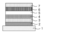
- 1 shows a specific structural example of the organic electroluminescence device.
- 1 is a substrate
- 2 is an anode
- 3 is a hole injection layer
- 4 is a hole transport layer
- 5 is a light emitting layer
- 6 is an electron transport layer
- 7 is a cathode.
- the organic light emitting element of the present invention is a multi-wavelength light emitting element
- the shortest wavelength light emission can include delayed fluorescence. It is also possible that the shortest wavelength emission does not include delayed fluorescence.
- the organic electroluminescence device of the present invention is held by a substrate, the substrate is not particularly limited and is commonly used in organic electroluminescence devices, such as glass, clear plastic, quartz and silicon. Any material formed by the above may be used.
- the anode of an organic electroluminescence device is manufactured from a metal, alloy, conductive compound or a combination thereof.
- the metal, alloy or conductive compound has a high work function (4 eV or higher).
- the metal is Au.
- the conductive transparent material is selected from CuI, indium tin oxide (ITO), SnO 2 and ZnO.
- an amorphous material capable of forming a transparent conductive film such as IDIXO (In 2 O 3-ZnO), is used.
- the anode is a thin film. In some embodiments, the thin film is made by vapor deposition or sputtering.
- the film is patterned by a photolithography method.
- the pattern may be formed using a mask having a shape suitable for vapor deposition or sputtering on the electrode material.
- a wet film forming method such as a printing method or a coating method is used.
- synchrotron radiation passes through the anode, the anode has a transmittance of greater than 10% and the anode has a sheet resistance of no more than a few hundred ohms per unit area.
- the thickness of the anode is 10-1,000 nm. In some embodiments, the thickness of the anode is 10-200 nm. In some embodiments, the thickness of the anode will vary depending on the material used.
- the cathode is made of an electrode material such as a metal with a low work function (4 eV or less) (referred to as an electron-injected metal), an alloy, a conductive compound or a combination thereof.
- the electrode material is sodium, sodium-potassium alloy, magnesium, lithium, magnesium-copper mixture, magnesium-silver mixture, magnesium-aluminum mixture, magnesium-indium mixture, aluminum-aluminum oxide (Al 2). O 3 ) Selected from mixtures, indium, lithium-aluminum mixtures and rare earth elements.
- a mixture of the electron-injected metal and a second metal which is a stable metal with a higher work function than the electron-injected metal, is used.
- the mixture is selected from a magnesium-silver mixture, a magnesium-aluminum mixture, a magnesium-indium mixture, an aluminum-aluminum oxide (Al 2 O 3 ) mixture, a lithium-aluminum mixture and aluminum.
- the mixture improves electron injection properties and resistance to oxidation.
- the cathode is manufactured by forming the electrode material as a thin film by vapor deposition or sputtering.
- the cathode has a sheet resistance of tens of ohms or less per unit area.
- the cathode has a thickness of 10 nm to 5 ⁇ m.
- the thickness of the cathode is 50-200 nm.
- any one of the anode and cathode of the organic electroluminescence element is transparent or translucent in order to transmit synchrotron radiation.
- the transparent or translucent electroluminescent device improves the light radiance.
- the cathode is formed of the conductive transparent material described above with respect to the anode to form a transparent or translucent cathode.
- the device comprises an anode and a cathode, both of which are transparent or translucent.
- the injection layer is the layer between the electrode and the organic layer. In some embodiments, the injection layer reduces the drive voltage and enhances the light radiance. In some embodiments, the injection layer comprises a hole injection layer and an electron injection layer. The injection layer can be arranged between the anode and the light emitting layer or the hole transport layer, and between the cathode and the light emitting layer or the electron transport layer. In some embodiments, an injection layer is present. In some embodiments, there is no injection layer. The following are examples of preferable compounds that can be used as hole injection materials.
- the barrier layer is a layer capable of preventing charges (electrons or holes) and / or excitons present in the light emitting layer from diffusing outside the light emitting layer.
- the electron barrier layer resides between the light emitting layer and the hole transport layer, preventing electrons from passing through the light emitting layer to the hole transport layer.
- the hole barrier layer exists between the light emitting layer and the electron transport layer to prevent holes from passing through the light emitting layer to the electron transport layer.
- the barrier layer prevents excitons from diffusing outside the light emitting layer.
- the electron barrier layer and the hole barrier layer constitute an exciton barrier layer.
- the term "electron barrier layer" or "exciton barrier layer” includes both an electron barrier layer and a layer having both the functions of an exciton barrier layer.
- Hole barrier layer functions as an electron transport layer. In some embodiments, the hole barrier layer prevents holes from reaching the electron transport layer during electron transport. In some embodiments, the hole barrier layer increases the probability of electron-hole recombination in the light emitting layer.
- the material used for the hole barrier layer may be the same material as described above for the electron transport layer. The following are examples of preferable compounds that can be used for the hole barrier layer.
- the electron barrier layer transports holes.
- the electron barrier layer blocks electrons from reaching the hole transport layer during hole transport.
- the electron barrier layer increases the probability of electron-hole recombination in the light emitting layer.
- the material used for the electron barrier layer may be the same material as described above for the hole transport layer. Specific examples of preferable compounds that can be used as an electron barrier material are given below.
- Exciton barrier layer prevents excitons generated through recombination of holes and electrons in the light emitting layer from diffusing to the charge transport layer. In some embodiments, the exciton barrier layer allows for effective exciton confinement in the light emitting layer. In some embodiments, the light emission efficiency of the device is improved. In some embodiments, the exciton barrier layer is adjacent to the light emitting layers on either the anode side and the cathode side, and on either side of the anode side. In some embodiments, when the exciton barrier layer is present on the anode side, the layer may be present between the hole transport layer and the light emitting layer and adjacent to the light emitting layer.
- the layer when the exciton barrier layer is present on the cathode side, the layer may be present between the light emitting layer and the cathode and adjacent to the light emitting layer.
- a hole injection layer, an electron barrier layer or a similar layer resides between the anode and the exciton barrier layer adjacent to the light emitting layer on the anode side.
- the hole injection layer, electron barrier layer, hole barrier layer or similar layer is present between the cathode and the exciton barrier layer adjacent to the light emitting layer on the cathode side.
- the excited element barrier layer comprises an excited singlet energy and an excited triplet energy, at least one of which is higher than the excited singlet energy and the excited triplet energy of the light emitting material, respectively.
- the hole transport layer contains a hole transport material.
- the hole transport layer is monolayer. In some embodiments, the hole transport layer has multiple layers. In some embodiments, the hole transport material has one of the hole injection or transport properties and the electron barrier properties. In some embodiments, the hole transport material is an organic material. In some embodiments, the hole transport material is an inorganic material. Examples of known hole transport materials that can be used in the present invention are, but are not limited to, triazole derivatives, oxadiazole derivatives, imidazole derivatives, carbazole derivatives, indolocarbazole derivatives, polyarylalkane inducers, pyrazoline derivatives, pyrazolones.
- the hole transport material is selected from porphyrin compounds, aromatic tertiary amine compounds and styrylamine compounds.
- the hole transport material is an aromatic tertiary amine compound. Specific examples of preferable compounds that can be used as hole transport materials are given below.
- Electron transport layer contains an electron transport material.
- the electron transport layer is monolayer.
- the electron transport layer has multiple layers.
- the electron transport material only needs to have the function of transporting the electrons injected from the cathode to the light emitting layer.
- the electron transport material also functions as a hole barrier material.
- electron transport layers examples include, but are not limited to, nitro-substituted fluorene derivatives, diphenylquinone derivatives, thiopyrandioxide derivatives, carbodiimides, fluorenylidene methane derivatives, anthracinodimethanes, anthrone derivatives, and oxadi. Examples thereof include azole derivatives, azole derivatives, azine derivatives or combinations thereof, or polymers thereof.
- the electron transport material is a thiadiazole inducer or a quinoxaline derivative.
- the electron transport material is a polymeric material. Specific examples of preferable compounds that can be used as electron transport materials are given below.
- preferable compounds as materials that can be added to each organic layer are given.
- it may be added as a stabilizing material.
- the light emitting layer is incorporated into the device.
- devices include, but are not limited to, OLED valves, OLED lamps, television displays, computer monitors, mobile phones and tablets.
- the electronic device comprises an OLED having an anode, a cathode, and at least one organic layer comprising a light emitting layer between the anode and the cathode.
- the components described herein can be incorporated into a variety of photosensitive or photoactivating devices, such as OLEDs or optoelectronic devices.
- the construct may be useful for facilitating charge transfer or energy transfer within the device and / or as a hole transport material.
- Examples of the device include an organic light emitting diode (OLED), an organic integrated line (OIC), an organic field effect transistor (O-FET), an organic thin film (O-TFT), an organic light emitting transistor (O-LET), and an organic solar cell. (O-SC), organic optical detectors, organic photoreceivers, organic field-quench devices (O-FQD), light emitting fuel cells (LECs) or organic laser diodes (O-lasers).
- OLED organic light emitting diode
- OIC organic integrated line
- O-FET organic field effect transistor
- OFTFT organic thin film
- O-LET organic light emitting transistor
- O-SC organic solar cell.
- O-SC organic solar cell.
- organic optical detectors organic photoreceivers
- O-FQD organic field-quench devices
- LOCs light emitting fuel cells
- O-lasers organic laser diodes
- the electronic device comprises an OLED comprising an anode, a cathode, and at least one organic layer comprising a light emitting layer between the anode and the cathode.
- the device comprises an OLED of different colors.
- the device comprises an array containing a combination of OLEDs.
- the combination of OLEDs is a combination of three colors (eg RGB).
- the combination of OLEDs is a combination of colors that are neither red nor green nor blue (eg, orange and yellow-green).
- the combination of OLEDs is a combination of two colors, four colors or more.
- the device is A circuit board having a first surface with a mounting surface and a second surface opposite the mounting surface and defining at least one opening.
- At least one OLED that has The housing for the circuit board and An OLED light comprising at least one connector located at the end of the housing, wherein the housing and the connector define a package suitable for mounting in lighting equipment.
- the OLED light has a plurality of OLEDs mounted on a circuit board such that light is emitted in multiple directions.
- some light emitted in the first direction is polarized and emitted in the second direction.
- a reflector is used to polarize the light emitted in the first direction.
- the light emitting layer of the present invention can be used in a screen or display.
- the compounds according to the invention are deposited onto a substrate using steps such as, but not limited to, vacuum evaporation, deposition, vapor deposition or chemical vapor deposition (CVD).
- the substrate is a photoplate structure useful in two-sided etching that provides pixels with a unique aspect ratio.
- the screen also referred to as a mask
- the design of the corresponding artwork pattern allows the placement of very steep, narrow tie bars between pixels in the vertical direction, as well as large, wide-ranging bevel openings in the horizontal direction.
- Pixel internal patterning makes it possible to construct 3D pixel openings with different aspect ratios in the horizontal and vertical directions.
- imaged "stripe" or halftone circles in the pixel area protects the etching in the particular area until these particular patterns are undercut and removed from the substrate. At that time, all the pixel regions are processed at the same etching rate, but the depth varies depending on the halftone pattern.
- By changing the size and spacing of the halftone patterns it is possible to etch with different protection rates within the pixel, allowing for the deep localized etching required to form steep vertical bevels. ..
- the preferred material for the vapor deposition mask is Invar.
- Invar is a metal alloy that is cold-rolled into a long thin sheet at a steel mill. Invar cannot be electrodeposited onto the spin mandrel as a nickel mask.
- a suitable and low-cost method for forming an opening region in a vapor deposition mask is a wet chemical etching method.
- the screen or display pattern is a pixel matrix on a substrate.
- the screen or display pattern is processed using lithography (eg, photolithography and e-beam lithography).
- the screen or display pattern is processed using wet chemical etching.
- the screen or display pattern is processed using plasma etching.
- the OLED display is generally manufactured by forming a large mother panel and then cutting the mother panel in cell panel units. Normally, each cell panel on the mother panel forms a thin film transistor (TFT) having an active layer and a source / drain electrode on a base substrate, a flattening film is applied to the TFT, and a pixel electrode and a light emitting layer are applied. , The counter electrode and the encapsulating layer are formed in order over time, and are formed by cutting from the mother panel.
- TFT thin film transistor
- the OLED display is generally manufactured by forming a large mother panel and then cutting the mother panel in cell panel units.
- each cell panel on the mother panel forms a thin film transistor (TFT) having an active layer and a source / drain electrode on a base substrate, a flattening film is applied to the TFT, and a pixel electrode and a light emitting layer are applied.
- TFT thin film transistor
- the counter electrode and the encapsulating layer are formed in order over time, and are formed by cutting from the mother panel.
- a method of manufacturing an organic light emitting diode (OLED) display is provided, wherein the method is: The process of forming a barrier layer on the base base material of the mother panel, A step of forming a plurality of display units on a cell panel unit on the barrier layer, A step of forming an encapsulation layer on each of the display units of the cell panel, A step of applying an organic film to the interface portion between the cell panels is included.
- the barrier layer is, for example, an inorganic film formed of SiNx, the edges of the barrier layer being coated with an organic film formed of polyimide or acrylic.
- the organic film helps the mother panel to be softly cut in cell panel units.
- the thin film transistor (TFT) layer comprises a light emitting layer, a gate electrode, and a source / drain electrode.
- Each of the plurality of display units may have a thin film transistor (TFT) layer, a flattening film formed on the TFT layer, and a light emitting unit formed on the flattening film, and the interface portion may have a light emitting unit.
- the applied organic film is formed of the same material as the flattening film, and is formed at the same time as the flattening film is formed.
- the light emitting unit is coupled to the TFT layer by a passivation layer, a flattening film in between, and an encapsulating layer that coats and protects the light emitting unit.
- the organic film is not coupled to either the display unit or the encapsulation layer.
- each of the organic film and the flattening film may contain any one of polyimide and acrylic.
- the barrier layer may be an inorganic film.
- the base substrate may be made of polyimide.
- the method further comprises a step of attaching a carrier substrate made of a glass material to the other surface of the base substrate before forming a barrier layer on one surface of the base substrate made of polyimide. It may include a step of separating the carrier substrate from the base substrate prior to cutting along the interface portion.
- the OLED display is a flexible display.
- the passivation layer is an organic film placed on the TFT layer for coating the TFT layer.
- the flattening film is an organic film formed on the passivation layer.
- the flattening film is made of polyimide or acrylic, similar to the organic film formed at the ends of the barrier layer. In some embodiments, the flattening film and the organic film are formed simultaneously during the manufacture of the OLED display. In some embodiments, the organic film may be formed at the edges of the barrier layer, whereby a portion of the organic film is in direct contact with the base substrate and the rest of the organic film is removed. , Surrounding the edge of the barrier layer and in contact with the barrier layer.
- the light emitting layer has a pixel electrode, a counter electrode, and an organic light emitting layer disposed between the pixel electrode and the counter electrode.
- the pixel electrode is connected to a source / drain electrode in the TFT layer.
- an appropriate voltage is formed between the pixel electrode and the counter electrode so that the organic light emitting layer emits light, thereby the image. Is formed.
- the image forming unit having the TFT layer and the light emitting unit will be referred to as a display unit.
- the encapsulation layer that covers the display unit and prevents the penetration of external moisture may be formed in a thin film encapsulation structure in which organic films and inorganic films are alternately laminated.
- the encapsulation layer has a thin film encapsulation structure in which a plurality of thin films are laminated.
- the organic film applied to the interface section is spaced apart from each of the plurality of display units.
- the organic film is formed in such a manner that some of the organic films are in direct contact with the base substrate and the rest of the organic film surrounds the edges of the barrier layer while in contact with the barrier layer. Will be done.
- the OLED display is flexible and uses a flexible base substrate made of polyimide.
- the base substrate is formed on a carrier substrate made of a glass material, which is then separated.
- the barrier layer is formed on the surface of the base substrate opposite the carrier substrate.
- the barrier layer is patterned according to the size of each cell panel. For example, a base substrate is formed on all surfaces of the mother panel, while a barrier layer is formed according to the size of each cell panel, thereby forming a groove in the interface portion between the barrier layers of the cell panel. Each cell panel can be cut along the groove.
- the manufacturing method further comprises the step of cutting along an interface portion, where a groove is formed in the barrier layer, at least a portion of the organic film is formed in the groove, and the groove is formed. Does not penetrate the base substrate.
- the TFT layer of each cell panel is formed and a passivation layer, which is an inorganic film, and a flattening film, which is an organic film, are placed on the TFT layer to cover the TFT layer.
- a polyimide or acrylic flattening film is formed, for example, the groove of the interface portion is covered with an organic film made of polyimide or acrylic, for example. This prevents cracking by allowing the organic film to absorb the impact generated when each cell panel is cut along the groove at the interface section.
- the groove of the interface portion between the barrier layers is covered with an organic film to absorb the impact that can be transmitted to the barrier layer without the organic film, so that each cell panel is softly cut and the barrier layer is used. It may be prevented from cracking.
- the organic film and the flattening film covering the grooves of the interface portion are arranged at intervals from each other.
- the organic film and the flattening film are interconnected as one layer, external moisture may infiltrate into the display unit through the flattening film and the portion where the organic film remains.
- the organic film and the flattening film are spaced apart from each other so that the organic film is spaced apart from the display unit.
- the display unit is formed by the formation of a light emitting unit and the encapsulation layer is placed on the display unit to cover the display unit.
- the carrier base material that supports the base base material is separated from the base base material.
- the carrier substrate is separated from the base substrate due to the difference in the coefficient of thermal expansion between the carrier substrate and the base substrate.
- the mother panel is cut in cell panel units.
- the mother panel is cut along the interface between the cell panels using a cutter.
- the grooves in the interface section where the mother panel is cut are covered with an organic film so that the organic film absorbs the impact during cutting.
- the barrier layer can be prevented from cracking during cutting. In some embodiments, the method reduces the defective rate of the product and stabilizes its quality.
- Another embodiment is a barrier layer formed on a base substrate, a display unit formed on the barrier layer, an encapsulating layer formed on the display unit, and an organic coating applied to the ends of the barrier layer.
- the materials, treatment contents, treatment procedures, etc. shown below can be appropriately changed as long as they do not deviate from the gist of the present invention. Therefore, the scope of the present invention should not be construed as limiting by the specific examples shown below.
- the emission characteristics are evaluated by a source meter (Caseley: 2400 series), a semiconductor parameter analyzer (Agilent Technology: E5273A), an optical power meter measuring device (Newport: 1930C), and an optical spectroscope.
- Each thin film was laminated with a vacuum degree of 1 ⁇ 10-6 Pa on a glass substrate having an anode made of indium tin oxide (ITO) having a film thickness of 100 nm formed by a vacuum vapor deposition method.
- ITO indium tin oxide
- HATCN was formed on ITO to a thickness of 10 nm
- NPD was formed on it to a thickness of 30 nm
- TrisPCz was further formed on it to a thickness of 10 nm.
- compound H3 was formed to a thickness of 3 nm.
- compound H3, compound T10, compound S1 and compound E1 were co-deposited from different vapor deposition sources at the concentrations shown in the table below to form a light emitting layer having a thickness of 30 nm.
- SF3TRZ was formed as a hole barrier layer having a thickness of 10 nm.
- SF3TRZ and Liq were co-deposited from different vapor deposition sources to form an electron transport layer having a thickness of 30 nm.
- SF3TRZ: Liq (weight ratio) was set to 7: 3. Further, Liq was formed to a thickness of 2 nm, and then aluminum (Al) was deposited to a thickness of 100 nm to form a cathode.
- each organic electroluminescence element was prepared by using the compound S2 and the compound S3 as the third compound, respectively. Each of these elements satisfied the conditions (a) to (e). From each of the organic electroluminescence devices of Examples 4 and 5, light emission with high color purity derived from the fourth organic compound is observed, and it is confirmed that the life is longer than that of Comparative Example 1.
- the present invention it is possible to provide an organic light emitting device having a high color purity and a long life. Therefore, the present invention has high industrial applicability.
Landscapes
- Chemical & Material Sciences (AREA)
- Organic Chemistry (AREA)
- Physics & Mathematics (AREA)
- Engineering & Computer Science (AREA)
- Materials Engineering (AREA)
- Spectroscopy & Molecular Physics (AREA)
- Optics & Photonics (AREA)
- Electroluminescent Light Sources (AREA)
- Plural Heterocyclic Compounds (AREA)
- Nitrogen Condensed Heterocyclic Rings (AREA)
Priority Applications (11)
| Application Number | Priority Date | Filing Date | Title |
|---|---|---|---|
| US17/999,979 US20230209847A1 (en) | 2020-05-29 | 2021-05-27 | Organic light emitting element |
| JP2022526632A JP7728589B2 (ja) | 2020-05-29 | 2021-05-27 | 有機発光素子 |
| KR1020227042509A KR102826039B1 (ko) | 2020-05-29 | 2021-05-27 | 유기 발광 소자 |
| CN202180038014.0A CN115669265A (zh) | 2020-05-29 | 2021-05-27 | 有机发光元件 |
| PCT/JP2021/034975 WO2022249506A1 (ja) | 2020-05-29 | 2021-09-24 | 化合物、発光材料および発光素子 |
| JP2023523948A JP7721169B2 (ja) | 2020-05-29 | 2021-09-24 | 化合物、発光材料および発光素子 |
| CN202180098537.4A CN117412976A (zh) | 2020-05-29 | 2021-09-24 | 化合物、发光材料及发光元件 |
| US18/564,003 US20240298538A1 (en) | 2020-05-29 | 2021-09-24 | Compound, light-emitting material, and light-emitting element |
| JP2023523947A JP7717401B2 (ja) | 2020-05-29 | 2021-09-24 | 化合物、発光材料および発光素子 |
| KR1020237041849A KR20240013139A (ko) | 2020-05-29 | 2021-09-24 | 화합물, 발광 재료 및 발광 소자 |
| PCT/JP2021/034974 WO2022249505A1 (ja) | 2020-05-29 | 2021-09-24 | 化合物、発光材料および発光素子 |
Applications Claiming Priority (2)
| Application Number | Priority Date | Filing Date | Title |
|---|---|---|---|
| JP2020094308 | 2020-05-29 | ||
| JP2020-094308 | 2020-05-29 |
Publications (1)
| Publication Number | Publication Date |
|---|---|
| WO2021241677A1 true WO2021241677A1 (ja) | 2021-12-02 |
Family
ID=78744898
Family Applications (3)
| Application Number | Title | Priority Date | Filing Date |
|---|---|---|---|
| PCT/JP2021/020163 Ceased WO2021241677A1 (ja) | 2020-05-29 | 2021-05-27 | 有機発光素子 |
| PCT/JP2021/034974 Ceased WO2022249505A1 (ja) | 2020-05-29 | 2021-09-24 | 化合物、発光材料および発光素子 |
| PCT/JP2021/034975 Ceased WO2022249506A1 (ja) | 2020-05-29 | 2021-09-24 | 化合物、発光材料および発光素子 |
Family Applications After (2)
| Application Number | Title | Priority Date | Filing Date |
|---|---|---|---|
| PCT/JP2021/034974 Ceased WO2022249505A1 (ja) | 2020-05-29 | 2021-09-24 | 化合物、発光材料および発光素子 |
| PCT/JP2021/034975 Ceased WO2022249506A1 (ja) | 2020-05-29 | 2021-09-24 | 化合物、発光材料および発光素子 |
Country Status (6)
| Country | Link |
|---|---|
| US (2) | US20230209847A1 (enExample) |
| JP (3) | JP7728589B2 (enExample) |
| KR (2) | KR102826039B1 (enExample) |
| CN (2) | CN115669265A (enExample) |
| TW (1) | TWI865782B (enExample) |
| WO (3) | WO2021241677A1 (enExample) |
Cited By (6)
| Publication number | Priority date | Publication date | Assignee | Title |
|---|---|---|---|---|
| WO2023167272A1 (ja) * | 2022-03-04 | 2023-09-07 | 株式会社Kyulux | 有機発光素子、遅延蛍光材料の評価方法、遅延蛍光材料の設計方法、有機発光素子の設計方法、およびプログラム |
| WO2023167271A1 (ja) * | 2022-03-04 | 2023-09-07 | 株式会社Kyulux | 有機発光素子、遅延蛍光材料の評価方法、遅延蛍光材料の設計方法、有機発光素子の設計方法、およびプログラム |
| WO2023167273A1 (ja) * | 2022-03-04 | 2023-09-07 | 株式会社Kyulux | 有機発光素子、遅延蛍光材料の評価方法、遅延蛍光材料の設計方法、有機発光素子の設計方法、およびプログラム |
| JP2023541977A (ja) * | 2020-09-18 | 2023-10-04 | 三星ディスプレイ株式會社 | 青色光を発する有機エレクトロルミネッセンス素子 |
| WO2024088239A1 (zh) * | 2022-10-28 | 2024-05-02 | 清华大学 | 一种有机化合物及采用该化合物的有机电致发光器 |
| WO2025205402A1 (ja) * | 2024-03-29 | 2025-10-02 | 出光興産株式会社 | 有機エレクトロルミネッセンス素子及び電子機器 |
Citations (3)
| Publication number | Priority date | Publication date | Assignee | Title |
|---|---|---|---|---|
| WO2014157619A1 (ja) * | 2013-03-29 | 2014-10-02 | 国立大学法人九州大学 | 有機エレクトロルミネッセンス素子 |
| WO2018070348A1 (ja) * | 2016-10-13 | 2018-04-19 | シャープ株式会社 | 表示装置およびその製造方法 |
| JP2019186521A (ja) * | 2018-03-30 | 2019-10-24 | キヤノン株式会社 | 有機発光素子、表示装置、撮像装置および照明装置 |
Family Cites Families (20)
| Publication number | Priority date | Publication date | Assignee | Title |
|---|---|---|---|---|
| JP2011105676A (ja) | 2009-11-19 | 2011-06-02 | Mitsubishi Chemicals Corp | 有機金属錯体、発光材料、有機電界発光素子材料、有機電界発光素子用組成物、有機電界発光素子、有機el表示装置及び有機el照明 |
| JP5366106B1 (ja) | 2012-04-09 | 2013-12-11 | 国立大学法人九州大学 | 有機発光素子ならびにそれに用いる発光材料および化合物 |
| KR102577829B1 (ko) | 2013-08-14 | 2023-09-12 | 가부시키가이샤 큐럭스 | 유기 일렉트로루미네선스 소자 |
| EP3266772B1 (de) * | 2016-07-06 | 2019-04-24 | Cynora Gmbh | Organische moleküle, insbesondere zur verwendung in optoelektronischen vorrichtungen |
| DE102016113277A1 (de) * | 2016-07-19 | 2018-01-25 | Cynora Gmbh | Organische Moleküle zur Verwendung in optoelektronischen Bauelementen |
| KR102207689B1 (ko) * | 2016-08-24 | 2021-01-25 | 시노라 게엠베하 | 유기 분자, 특히 유기 광전자 디바이스에 사용하기 위한 유기 분자 |
| CN107778214B (zh) * | 2016-08-25 | 2020-03-31 | 西诺拉股份有限公司 | 有机分子,特别是用于有机光电器件的有机分子 |
| KR102490154B1 (ko) | 2016-12-21 | 2023-01-18 | 고쿠리쓰다이가쿠호진 규슈다이가쿠 | 발광 재료, 화합물 및 유기 발광 소자 |
| JP2018111751A (ja) | 2017-01-10 | 2018-07-19 | 国立大学法人九州大学 | 発光材料、化合物および有機発光素子 |
| JP7226806B2 (ja) * | 2017-06-23 | 2023-02-21 | 株式会社Kyulux | 有機発光ダイオードに用いられる組成物 |
| US11584739B2 (en) * | 2017-06-23 | 2023-02-21 | Kyulux, Inc. | Composition of matter for use in organic light-emitting diodes |
| DE102017114345B4 (de) | 2017-06-28 | 2019-01-17 | Cynora Gmbh | Organische Moleküle, insbesondere zur Verwendung in organischen optoelektronischen Vorrichtungen |
| US11069860B2 (en) | 2017-08-21 | 2021-07-20 | Kyulux, Inc. | Composition of matter for use in organic light-emitting diodes |
| DE102018114290B3 (de) | 2018-06-14 | 2019-06-06 | Cynora Gmbh | Organische Moleküle, insbesondere zur Verwendung in optoelektronischen Vorrichtungen |
| CN110759851A (zh) * | 2018-07-25 | 2020-02-07 | 北京鼎材科技有限公司 | 一种有机电致发光材料及其应用 |
| JP7325731B2 (ja) * | 2018-08-23 | 2023-08-15 | 国立大学法人九州大学 | 有機エレクトロルミネッセンス素子 |
| EP3670508B1 (en) * | 2018-12-20 | 2025-10-01 | Samsung Display Co., Ltd. | Organic molecules for use in optoelectronic devices |
| TWI851806B (zh) | 2019-09-05 | 2024-08-11 | 日商九州有機光材股份有限公司 | 用於有機發光二極體之物質組成物 |
| KR20210050829A (ko) * | 2019-10-29 | 2021-05-10 | 솔브레인 주식회사 | 화합물 및 이를 포함하는 유기 발광 소자 |
| KR102793989B1 (ko) * | 2019-11-08 | 2025-04-15 | 삼성디스플레이 주식회사 | 유기 전계 발광 소자 및 유기 전계 발광 소자용 방향족 화합물 |
-
2021
- 2021-05-27 CN CN202180038014.0A patent/CN115669265A/zh active Pending
- 2021-05-27 US US17/999,979 patent/US20230209847A1/en active Pending
- 2021-05-27 JP JP2022526632A patent/JP7728589B2/ja active Active
- 2021-05-27 KR KR1020227042509A patent/KR102826039B1/ko active Active
- 2021-05-27 WO PCT/JP2021/020163 patent/WO2021241677A1/ja not_active Ceased
- 2021-05-28 TW TW110119397A patent/TWI865782B/zh active
- 2021-09-24 KR KR1020237041849A patent/KR20240013139A/ko active Pending
- 2021-09-24 JP JP2023523947A patent/JP7717401B2/ja active Active
- 2021-09-24 JP JP2023523948A patent/JP7721169B2/ja active Active
- 2021-09-24 CN CN202180098537.4A patent/CN117412976A/zh active Pending
- 2021-09-24 WO PCT/JP2021/034974 patent/WO2022249505A1/ja not_active Ceased
- 2021-09-24 US US18/564,003 patent/US20240298538A1/en active Pending
- 2021-09-24 WO PCT/JP2021/034975 patent/WO2022249506A1/ja not_active Ceased
Patent Citations (3)
| Publication number | Priority date | Publication date | Assignee | Title |
|---|---|---|---|---|
| WO2014157619A1 (ja) * | 2013-03-29 | 2014-10-02 | 国立大学法人九州大学 | 有機エレクトロルミネッセンス素子 |
| WO2018070348A1 (ja) * | 2016-10-13 | 2018-04-19 | シャープ株式会社 | 表示装置およびその製造方法 |
| JP2019186521A (ja) * | 2018-03-30 | 2019-10-24 | キヤノン株式会社 | 有機発光素子、表示装置、撮像装置および照明装置 |
Cited By (16)
| Publication number | Priority date | Publication date | Assignee | Title |
|---|---|---|---|---|
| JP2023541977A (ja) * | 2020-09-18 | 2023-10-04 | 三星ディスプレイ株式會社 | 青色光を発する有機エレクトロルミネッセンス素子 |
| JP7512522B2 (ja) | 2020-09-18 | 2024-07-08 | 三星ディスプレイ株式會社 | 有機エレクトロルミネッセンス素子および光発生方法 |
| JP2023129092A (ja) * | 2022-03-04 | 2023-09-14 | 株式会社Kyulux | 有機発光素子、遅延蛍光材料の評価方法、遅延蛍光材料の設計方法、有機発光素子の設計方法、およびプログラム |
| EP4489552A4 (en) * | 2022-03-04 | 2025-06-11 | Kyulux, Inc. | ORGANIC ELECTROLUMINESCENT ELEMENT, METHOD FOR EVALUATING DELAYED FLUORESCENCE MATERIAL, METHOD FOR DESIGNING DELAYED FLUORESCENCE MATERIAL, METHOD FOR DESIGNING ORGANIC ELECTROLUMINESCENT ELEMENT, AND PROGRAM |
| WO2023167272A1 (ja) * | 2022-03-04 | 2023-09-07 | 株式会社Kyulux | 有機発光素子、遅延蛍光材料の評価方法、遅延蛍光材料の設計方法、有機発光素子の設計方法、およびプログラム |
| JP2023129094A (ja) * | 2022-03-04 | 2023-09-14 | 株式会社Kyulux | 有機発光素子、遅延蛍光材料の評価方法、遅延蛍光材料の設計方法、有機発光素子の設計方法、およびプログラム |
| WO2023167273A1 (ja) * | 2022-03-04 | 2023-09-07 | 株式会社Kyulux | 有機発光素子、遅延蛍光材料の評価方法、遅延蛍光材料の設計方法、有機発光素子の設計方法、およびプログラム |
| JP7780191B2 (ja) | 2022-03-04 | 2025-12-04 | 株式会社Kyulux | 有機発光素子、遅延蛍光材料の評価方法、遅延蛍光材料の設計方法、有機発光素子の設計方法、およびプログラム |
| WO2023167271A1 (ja) * | 2022-03-04 | 2023-09-07 | 株式会社Kyulux | 有機発光素子、遅延蛍光材料の評価方法、遅延蛍光材料の設計方法、有機発光素子の設計方法、およびプログラム |
| JP2023129093A (ja) * | 2022-03-04 | 2023-09-14 | 株式会社Kyulux | 有機発光素子、遅延蛍光材料の評価方法、遅延蛍光材料の設計方法、有機発光素子の設計方法、およびプログラム |
| EP4489554A4 (en) * | 2022-03-04 | 2025-06-11 | Kyulux, Inc. | ORGANIC ELECTROLUMINESCENT ELEMENT, METHOD FOR EVALUATING DELAYED FLUORESCENCE MATERIAL, METHOD FOR DESIGNING DELAYED FLUORESCENCE MATERIAL, METHOD FOR DESIGNING ORGANIC ELECTROLUMINESCENT ELEMENT, AND PROGRAM |
| EP4489553A4 (en) * | 2022-03-04 | 2025-07-23 | Kyulux Inc | ORGANIC ELECTROLUMINESCENT ELEMENT, METHOD FOR EVALUATING DELAYED FLUORESCENCE MATERIAL, METHOD FOR DESIGNING DELAYED FLUORESCENCE MATERIAL, METHOD FOR DESIGNING ORGANIC ELECTROLUMINESCENT ELEMENT, AND PROGRAM |
| JP7780189B2 (ja) | 2022-03-04 | 2025-12-04 | 株式会社Kyulux | 有機発光素子、遅延蛍光材料の評価方法、遅延蛍光材料の設計方法、有機発光素子の設計方法、およびプログラム |
| JP7780190B2 (ja) | 2022-03-04 | 2025-12-04 | 株式会社Kyulux | 有機発光素子、遅延蛍光材料の評価方法、遅延蛍光材料の設計方法、有機発光素子の設計方法、およびプログラム |
| WO2024088239A1 (zh) * | 2022-10-28 | 2024-05-02 | 清华大学 | 一种有机化合物及采用该化合物的有机电致发光器 |
| WO2025205402A1 (ja) * | 2024-03-29 | 2025-10-02 | 出光興産株式会社 | 有機エレクトロルミネッセンス素子及び電子機器 |
Also Published As
| Publication number | Publication date |
|---|---|
| WO2022249505A1 (ja) | 2022-12-01 |
| JP7721169B2 (ja) | 2025-08-12 |
| CN115669265A (zh) | 2023-01-31 |
| JPWO2021241677A1 (enExample) | 2021-12-02 |
| TWI865782B (zh) | 2024-12-11 |
| JP7728589B2 (ja) | 2025-08-25 |
| US20240298538A1 (en) | 2024-09-05 |
| TW202204319A (zh) | 2022-02-01 |
| KR20230035234A (ko) | 2023-03-13 |
| US20230209847A1 (en) | 2023-06-29 |
| WO2022249506A1 (ja) | 2022-12-01 |
| JPWO2022249506A1 (enExample) | 2022-12-01 |
| JP7717401B2 (ja) | 2025-08-04 |
| JPWO2022249505A1 (enExample) | 2022-12-01 |
| KR20240013139A (ko) | 2024-01-30 |
| CN117412976A (zh) | 2024-01-16 |
| KR102826039B1 (ko) | 2025-06-26 |
Similar Documents
| Publication | Publication Date | Title |
|---|---|---|
| JP7418794B2 (ja) | 有機発光素子 | |
| JP7728589B2 (ja) | 有機発光素子 | |
| WO2021157642A1 (ja) | ホスト材料、組成物および有機発光素子 | |
| EP4369886A1 (en) | Organic light-emitting element and design method therefor | |
| WO2022009790A1 (ja) | 有機発光素子 | |
| US20240315133A1 (en) | Organic light emitting device and method of producing same | |
| KR20230137918A (ko) | 유기 일렉트로 루미네선스 소자, 발광 조성물의 설계방법 및 프로그램 | |
| JP7630160B2 (ja) | 有機発光素子 | |
| EP4343875A1 (en) | Organic light emitting element | |
| JP7461095B1 (ja) | 有機発光素子、その設計方法およびプログラム | |
| TWI906500B (zh) | 有機發光元件及其製造方法 | |
| JP2020077872A (ja) | 電荷輸送材料、化合物および有機発光素子 | |
| WO2022230573A1 (ja) | 有機発光素子およびその製造方法 | |
| WO2022107798A1 (ja) | 有機エレクトロルミネッセンス素子、発光組成物の設計方法およびプログラム | |
| TW202403015A (zh) | 有機發光元件、延遲螢光材料的評價方法、延遲螢光材料的設計方法、有機發光元件的設計方法及程式 |
Legal Events
| Date | Code | Title | Description |
|---|---|---|---|
| 121 | Ep: the epo has been informed by wipo that ep was designated in this application |
Ref document number: 21813885 Country of ref document: EP Kind code of ref document: A1 |
|
| ENP | Entry into the national phase |
Ref document number: 2022526632 Country of ref document: JP Kind code of ref document: A |
|
| NENP | Non-entry into the national phase |
Ref country code: DE |
|
| 122 | Ep: pct application non-entry in european phase |
Ref document number: 21813885 Country of ref document: EP Kind code of ref document: A1 |