WO2021229991A1 - 信号伝送線路及び信号伝送線路の製造方法 - Google Patents
信号伝送線路及び信号伝送線路の製造方法 Download PDFInfo
- Publication number
- WO2021229991A1 WO2021229991A1 PCT/JP2021/015484 JP2021015484W WO2021229991A1 WO 2021229991 A1 WO2021229991 A1 WO 2021229991A1 JP 2021015484 W JP2021015484 W JP 2021015484W WO 2021229991 A1 WO2021229991 A1 WO 2021229991A1
- Authority
- WO
- WIPO (PCT)
- Prior art keywords
- conductor layer
- laminate
- transmission line
- signal transmission
- laminated body
- Prior art date
- Legal status (The legal status is an assumption and is not a legal conclusion. Google has not performed a legal analysis and makes no representation as to the accuracy of the status listed.)
- Ceased
Links
Images






Classifications
-
- H—ELECTRICITY
- H01—ELECTRIC ELEMENTS
- H01P—WAVEGUIDES; RESONATORS, LINES, OR OTHER DEVICES OF THE WAVEGUIDE TYPE
- H01P3/00—Waveguides; Transmission lines of the waveguide type
- H01P3/02—Waveguides; Transmission lines of the waveguide type with two longitudinal conductors
- H01P3/08—Microstrips; Strip lines
- H01P3/081—Microstriplines
- H01P3/082—Multilayer dielectric
-
- H—ELECTRICITY
- H01—ELECTRIC ELEMENTS
- H01P—WAVEGUIDES; RESONATORS, LINES, OR OTHER DEVICES OF THE WAVEGUIDE TYPE
- H01P3/00—Waveguides; Transmission lines of the waveguide type
- H01P3/02—Waveguides; Transmission lines of the waveguide type with two longitudinal conductors
- H01P3/08—Microstrips; Strip lines
-
- H—ELECTRICITY
- H01—ELECTRIC ELEMENTS
- H01P—WAVEGUIDES; RESONATORS, LINES, OR OTHER DEVICES OF THE WAVEGUIDE TYPE
- H01P3/00—Waveguides; Transmission lines of the waveguide type
- H01P3/02—Waveguides; Transmission lines of the waveguide type with two longitudinal conductors
- H01P3/08—Microstrips; Strip lines
- H01P3/085—Triplate lines
-
- H—ELECTRICITY
- H01—ELECTRIC ELEMENTS
- H01P—WAVEGUIDES; RESONATORS, LINES, OR OTHER DEVICES OF THE WAVEGUIDE TYPE
- H01P3/00—Waveguides; Transmission lines of the waveguide type
- H01P3/02—Waveguides; Transmission lines of the waveguide type with two longitudinal conductors
- H01P3/08—Microstrips; Strip lines
- H01P3/088—Stacked transmission lines
-
- H—ELECTRICITY
- H05—ELECTRIC TECHNIQUES NOT OTHERWISE PROVIDED FOR
- H05K—PRINTED CIRCUITS; CASINGS OR CONSTRUCTIONAL DETAILS OF ELECTRIC APPARATUS; MANUFACTURE OF ASSEMBLAGES OF ELECTRICAL COMPONENTS
- H05K1/00—Printed circuits
- H05K1/02—Details
-
- H—ELECTRICITY
- H05—ELECTRIC TECHNIQUES NOT OTHERWISE PROVIDED FOR
- H05K—PRINTED CIRCUITS; CASINGS OR CONSTRUCTIONAL DETAILS OF ELECTRIC APPARATUS; MANUFACTURE OF ASSEMBLAGES OF ELECTRICAL COMPONENTS
- H05K3/00—Apparatus or processes for manufacturing printed circuits
Definitions
- the present invention relates to a signal transmission line including a signal conductor layer and a ground conductor layer.
- the signal transmission line described in Patent Document 1 includes a laminate, a signal conductor, a first ground conductor, and a second ground conductor.
- the laminated body has a structure in which a plurality of resin sheets are laminated in the vertical direction.
- the laminate has flexibility.
- the signal conductor, the first ground conductor and the second ground conductor are provided in the laminated body.
- the first ground conductor is arranged on the signal conductor.
- the second ground conductor is located below the signal conductor.
- a gap is provided between the first ground conductor and the signal conductor.
- a gap is provided between the second ground conductor and the signal conductor.
- the characteristic impedance of the signal transmission line changes. More specifically, a gap is provided between the first ground conductor and the signal conductor. Therefore, the void overlaps with the first ground conductor and the signal conductor when viewed downward. In this case, when the void is deformed, the distance between the first ground conductor and the signal conductor changes. Then, the capacitance value between the first ground conductor and the signal conductor changes. As a result, the characteristic impedance of the signal transmission line changes.
- an object of the present invention is to provide a signal transmission line capable of suppressing a change in the characteristic impedance of the signal transmission line.
- the signal transmission line is It is a signal transmission line A laminate having a structure in which a plurality of insulating resin layers are laminated in the vertical direction of the laminate, A first signal conductor layer provided on the laminated body, the first signal conductor layer extending in the front-rear direction of the stack, and A first ground conductor layer provided on the laminate, which is above the first signal conductor layer in the vertical direction of the laminate so as to overlap the first signal conductor layer when viewed downward from the laminate.
- the arranged first ground conductor layer and A second ground conductor layer provided on the laminate which is below the first signal conductor layer in the vertical direction of the laminate so as to overlap the first signal conductor layer when viewed downward from the laminate.
- the second ground conductor layer arranged in The first interlayer connecting conductor provided in the laminated body so as to be located on the left side of the laminated body of the first signal conductor layer, the first ground conductor layer and the second ground conductor layer.
- the first interlayer connection conductor that electrically connects the A second interlayer connecting conductor provided in the laminated body so as to be located on the right side of the laminated body in the left-right direction of the first signal conductor layer, the first ground conductor layer and the second ground conductor layer.
- a second interlayer connection conductor that electrically connects to and Equipped with The first ground conductor layer is provided with a conductor non-forming portion in which the conductor layer does not exist.
- the laminate is provided with voids in which the insulating resin does not exist.
- At least a part of the non-conductor forming portion is to the right of the first interlayer connection conductor in the left-right direction of the laminate and to the left of the second interlayer connection conductor in the left-right direction of the laminate when viewed downward from the laminate. It is located in the first area located in At least a part of the void overlaps with the conductor non-forming portion in the first region when viewed downward from the laminated body, and is above the first signal conductor layer in the vertical direction of the laminated body. It is arranged below the first ground conductor layer in the vertical direction of the laminated body. The first region is not provided with an interlayer connecting conductor that electrically connects the first ground conductor layer and the second ground conductor layer.
- the shafts and members extending in the front-rear direction do not necessarily indicate only the shafts and members that are parallel to the front-rear direction.
- a shaft or member extending in the front-rear direction is a shaft or member inclined in a range of ⁇ 45 ° with respect to the front-back direction.
- a shaft or member extending in the vertical direction is a shaft or member inclined in a range of ⁇ 45 ° with respect to the vertical direction.
- a shaft or member extending in the left-right direction is a shaft or member inclined in a range of ⁇ 45 ° with respect to the left-right direction.
- the first member to the third member means a member or the like provided in the signal transmission line.
- each part of the first member is defined as follows in the present specification.
- the front portion of the first member means the front half of the first member.
- the rear part of the first member means the rear half of the first member.
- the left portion of the first member means the left half of the first member.
- the right portion of the first member means the right half of the first member.
- the upper part of the first member means the upper half of the first member.
- the lower part of the first member means the lower half of the first member.
- the front end of the first member means the front end of the first member.
- the rear end of the first member means the rear end of the first member.
- the left end of the first member means the left end of the first member.
- the right end of the first member means the right end of the first member.
- the upper end of the first member means the upper end of the first member.
- the lower end of the first member means the lower end of the first member.
- the front end portion of the first member means the front end of the first member and its vicinity.
- the rear end portion of the first member means the rear end of the first member and its vicinity.
- the left end portion of the first member means the left end portion of the first member and its vicinity.
- the right end portion of the first member means the right end portion of the first member and its vicinity.
- the upper end portion of the first member means the upper end portion of the first member and its vicinity.
- the lower end portion of the first member means the lower end portion of the first member and its vicinity.
- first member When any two members in the present specification are defined as a first member and a second member, the relationship between the two members has the following meaning.
- the fact that the first member is supported by the second member means that the first member is immovably attached to (that is, fixed) to the second member with respect to the second member. This includes the case where the first member is movably attached to the second member with respect to the second member. Further, the first member is supported by the second member when the first member is directly attached to the second member and when the first member is attached to the second member via the third member. Includes both if.
- the term that the first member is fixed to the second member includes the case where the first member is immovably attached to the second member with respect to the second member, and the first member is attached to the second member. It does not include the case where it is movably attached to the second member with respect to the second member. Further, the first member is fixed to the second member when the first member is directly attached to the second member and the first member is attached to the second member via the third member. Includes both if.
- the first member and the second member are electrically connected means that a direct current can flow between the first member and the second member. Therefore, the first member and the second member may be in contact with each other, or the first member and the second member may not be in contact with each other. When the first member and the second member are not in contact with each other, a third member having conductivity is arranged between the first member and the second member.
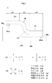
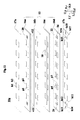
- FIG. 1 is a front view of the electronic device 1.
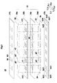
- FIG. 2 is an external perspective view of the signal transmission line 10.
- FIG. 3 is an exploded perspective view of the signal transmission line 10.
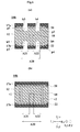
- FIG. 4A is a cross-sectional view taken along the line AA of FIG.
- FIG. 4B is a cross-sectional view taken along the line BB of FIG.
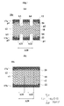
- FIG. 5 is a cross-sectional view taken along the line BB of the signal transmission line 10a.
- FIG. 6A is a cross-sectional view taken along the line AA of the signal transmission line 10b.
- FIG. 6B is a cross-sectional view taken along the line BB of the signal transmission line 10b.
- FIG. 7A is a cross-sectional view taken along the line AA of the signal transmission line 10c.
- FIG. 7B is a cross-sectional view taken along the line BB of the signal transmission line 10c.
- FIG. 8 is an exploded perspective view of the signal transmission line 10d.
- FIG. 9 is an exploded perspective view of the signal transmission line 10e.
- FIG. 10 is an exploded perspective view of the signal transmission line 10f.
- FIG. 11 is a perspective view of the signal transmission line 10 g.
- FIG. 12 is an exploded perspective view of the signal transmission line 10 g.
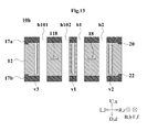
- FIG. 13 is a cross-sectional view of the signal transmission line 10h.
- FIG. 14 is a cross-sectional view of the signal transmission line 10i.
- FIG. 1 is a front view of the electronic device 1.
- FIG. 2 is an external perspective view of the signal transmission line 10.
- FIG. 3 is an exploded perspective view of the signal transmission line 10.
- FIG. 4A is a cross-sectional view taken along the line AA of FIG.
- FIG. 4B is a cross-sectional view taken along the line BB of FIG.
- the signal transmission line 10 is used to connect two circuits in an electronic device 1 such as a mobile phone. Further, as shown in FIG. 1, the signal transmission line 10 is used by being bent in the vertical direction. Therefore, the signal transmission line 10 has non-curved sections A1 and A3 and curved sections A2.
- the non-curved sections A1 and A3 are sections in which the signal transmission line 10 cannot be bent in the vertical direction.
- the curved section A2 is a section in which the signal transmission line 10 is bent in the vertical direction.
- the non-curved section A1 is located to the left of the curved section A2.
- the non-curved section A1 is adjacent to the curved section A2.
- the non-curved section A3 is located to the right of the curved section A2.
- the non-curved section A3 is adjacent to the curved section A2.
- the direction is defined as follows.
- the stacking direction of the laminated body 12 of the signal transmission line 10 is defined as the vertical direction of the laminated body.
- the direction in which the first signal conductor layer 18 of the signal transmission line 10 extends is defined as the front-rear direction of the laminated body.
- the line width direction of the first signal conductor layer 18 of the signal transmission line 10 is defined as the left-right direction of the laminated body.
- the vertical direction of the laminated body, the front-rear direction of the laminated body, and the horizontal direction of the laminated body are orthogonal to each other.
- the signal transmission line 10 is bent in the vertical direction. Therefore, the vertical direction of the laminated body and the front-back direction of the laminated body differ depending on the position of the signal transmission line 10, as shown in FIG.
- the non-curved sections A1 and A3 for example, the position of (1)
- the vertical direction of the laminated body and the front-back direction of the laminated body coincide with the vertical direction and the front-back direction, respectively.
- the curved section A2 for example, the position of (2) in which the laminated body 12 is bent, the vertical direction of the laminated body and the front-rear direction of the laminated body do not coincide with the vertical direction and the front-back direction, respectively.
- the definition of direction in this specification is an example. Therefore, it is not necessary that the direction of the signal transmission line 10 in actual use and the direction in the present specification match.
- the signal transmission line 10 is used to connect two circuits in an electronic device such as a mobile phone, for example.
- the signal transmission line 10 includes a laminate 12, resist layers 17a and 17b, a first signal conductor layer 18, a first ground conductor layer 20, a second ground conductor layer 22, and an external electrode 24. , 26, a plurality of first interlayer connection conductors v1, a plurality of second interlayer connection conductors v2, and a plurality of interlayer connection conductors v11, v12.
- FIGS. 2 and 3 typical layers among a plurality of first interlayer connection conductors v1, a plurality of second interlayer connection conductors v2, a plurality of conductor non-forming portions p1 and p2, and a plurality of voids h1 and h2. Reference symbols have been added to the connecting conductors, non-forming conductors and voids.
- the laminated body 12 has a plate shape. As shown in FIG. 2, the laminated body 12 has a rectangular shape having a long side extending in the front-rear direction of the laminated body when viewed downward from the laminated body. Therefore, the length of the laminated body 12 in the front-rear direction of the laminated body is longer than the length of the laminated body 12 in the left-right direction of the laminated body. The length of the laminated body 12 in the front-rear direction of the laminated body is longer than the length of the laminated body 12 in the vertical direction of the laminated body.
- the laminate 12 has flexibility. Therefore, the laminated body 12 is used in the electronic device 1 in a state of being bent in the vertical direction.
- the laminated body 12 has a structure in which insulating resin layers 16a to 16d are laminated in the vertical direction of the laminated body.
- the insulating resin layers 16a to 16d are laminated so as to be arranged in this order from top to bottom in the vertical direction of the laminated body.
- the insulating resin layers 16a to 16d are flexible dielectric sheets.
- the material of the insulating resin layers 16a to 16d is a thermoplastic resin such as polyimide or a liquid crystal polymer.
- the insulating resin layers 16a to 16d have the same rectangular shape as the laminated body 12 when viewed downward from the laminated body.
- the first signal conductor layer 18 is provided on the laminated body 12. More specifically, the first signal conductor layer 18 is provided on the upper surface of the insulating resin layer 16c. As a result, the first signal conductor layer 18 is provided in the laminated body 12.
- the first signal conductor layer 18 has a linear shape extending in the front-rear direction of the laminated body.
- the first signal conductor layer 18 is arranged at the center of the upper surface of the insulating resin layer 16c in the left-right direction of the laminate.
- the front end of the first signal conductor layer 18 is located at the front end of the insulating resin layer 16c.
- the rear end of the first signal conductor layer 18 is located at the rear end of the insulating resin layer 16c.
- a high frequency signal is transmitted to the first signal conductor layer 18.
- the first ground conductor layer 20 is provided on the laminated body 12.
- the first ground conductor layer 20 is arranged above the first signal conductor layer 18 in the vertical direction of the laminate so as to overlap the first signal conductor layer 18 when viewed downward from the laminate.
- “the first ground conductor layer 20 is arranged above the first signal conductor layer 18 in the vertical direction of the laminate” refers to the following state. At least a part of the first ground conductor layer 20 is arranged in a region through which the first signal conductor layer 18 passes when translated in the upward direction of the laminate.
- the first ground conductor layer 20 may be contained in the region through which the first signal conductor layer 18 passes when the first signal conductor layer 18 is translated in the upward direction of the laminated body, or the first signal conductor layer 18 may be contained in the upward direction of the laminated body. It may project from the area through which it passes when translating. In the present embodiment, the first ground conductor layer 20 protrudes from the region through which the first signal conductor layer 18 passes when it is translated in the upward direction of the laminate.
- the first ground conductor layer 20 is provided on the upper surface of the insulating resin layer 16a. As shown in FIG. 3, the first ground conductor layer 20 has a rectangular shape having a long side extending in the front-rear direction of the laminated body when viewed downward from the laminated body. The first ground conductor layer 20 has a shape that substantially matches the laminated body 12 when viewed downward from the laminated body. However, the first ground conductor layer 20 is slightly smaller than the laminated body 12 when viewed downward from the laminated body. A ground potential is connected to the first ground conductor layer 20.
- the second ground conductor layer 22 is provided on the laminated body 12.
- the second ground conductor layer 22 is arranged below the first signal conductor layer 18 so as to overlap the first signal conductor layer 18 when viewed downward from the laminate. More specifically, the second ground conductor layer 22 is provided on the lower surface of the insulating resin layer 16d.
- the second ground conductor layer 22 has a rectangular shape having a long side extending in the front-rear direction of the laminated body when viewed downward from the laminated body.
- the second ground conductor layer 22 has a shape that substantially matches the laminated body 12 when viewed downward from the laminated body. However, the second ground conductor layer 22 is slightly smaller than the laminated body 12 when viewed downward from the laminated body.
- a ground potential is connected to the second ground conductor layer 22.
- the first signal conductor layer 18, the first ground conductor layer 20, and the second ground conductor layer 22 have a stripline structure.
- the external electrode 24 is provided on the lower surface of the left end portion of the insulating resin layer 16d.
- the external electrode 24 has a rectangular shape when viewed downward from the laminate.
- the second ground conductor layer 22 is not provided around the external electrode 24 so that the external electrode 24 is insulated from the second ground conductor layer 22.
- the external electrode 24 overlaps the front end portion of the first signal conductor layer 18 when viewed downward from the laminate.
- the high frequency signal is input / output to the first signal conductor layer 18 via the external electrode 24.
- the external electrode 26 has a structure symmetrical to that of the external electrode 24. Therefore, the description of the external electrode 26 will be omitted.
- the resist layers 17a and 17b are flexible protective layers.
- the resist layers 17a and 17b have the same rectangular shape as the laminated body 12 when viewed downward from the laminated body.
- the resist layers 17a and 17b are not a part of the laminated body 12.
- the resist layer 17a covers the entire upper surface of the insulating resin layer 16a. As a result, the resist layer 17a protects the first ground conductor layer 20.
- the resist layer 17b covers substantially the entire lower surface of the insulating resin layer 16d. As a result, the resist layer 17b protects the second ground conductor layer 22. However, the resist layer 17b is provided with openings h11 to h18. The opening h11 overlaps with the external electrode 24 when viewed downward from the laminated body. As a result, the external electrode 24 is exposed to the outside from the signal transmission line 10 through the opening h11.
- the opening h12 is provided on the right side of the laminated body of the opening h11 in the left-right direction.
- the opening h13 is provided in front of the opening h11 in the front-rear direction of the laminated body.
- the opening h14 is provided on the left side of the laminated body of the opening h11 in the left-right direction. As a result, the second ground conductor layer 22 is exposed to the outside from the signal transmission line 10 through the openings h12 to h14.
- the openings h15 to h18 have a structure symmetrical with the openings h11 to h14, respectively. Therefore, the description of the openings h15 to h18 will be omitted.
- the first signal conductor layer 18, the first ground conductor layer 20, the second ground conductor layer 22, and the external electrodes 24, 26 as described above are, for example, copper foils provided on the upper surface or the lower surface of the insulating resin layers 16a to 16d. Is formed by etching.
- the plurality of first interlayer connecting conductors v1 are provided in the laminated body 12 so as to be located on the left side of the laminated body in the left-right direction of the first signal conductor layer 18.
- the plurality of first interlayer connecting conductors v1 are arranged so as to be arranged in a line at equal intervals in the front-rear direction of the laminated body.
- the plurality of first interlayer connecting conductors v1 penetrate the insulating resin layers 16a to 16d in the vertical direction.
- the upper ends of the plurality of first interlayer connecting conductors v1 are connected to the first ground conductor layer 20.
- the lower ends of the plurality of first interlayer connecting conductors v1 are connected to the second ground conductor layer 22.
- the plurality of first interlayer connecting conductors v1 electrically connect the first ground conductor layer 20 and the second ground conductor layer 22.
- the plurality of second interlayer connecting conductors v2 are provided in the laminated body 12 so as to be located on the right side of the laminated body in the left-right direction of the first signal conductor layer 18.
- the plurality of second interlayer connecting conductors v2 are arranged so as to be arranged in a line at equal intervals in the front-rear direction of the laminated body.
- the plurality of second interlayer connecting conductors v2 penetrate the insulating resin layers 16a to 16d in the vertical direction.
- the upper ends of the plurality of second interlayer connecting conductors v2 are connected to the first ground conductor layer 20.
- the lower ends of the plurality of second interlayer connecting conductors v2 are connected to the second ground conductor layer 22.
- the plurality of second interlayer connecting conductors v2 electrically connect the first ground conductor layer 20 and the second ground conductor layer 22.
- the interlayer connection conductor v11 is provided at the front end portion of the insulating resin layers 16a to 16d.
- the interlayer connection conductor v11 penetrates the insulating resin layers 16a to 16d in the vertical direction.
- the intermediate portion of the interlayer connection conductor v11 is connected to the front end portion of the first signal conductor layer 18.
- the lower end of the interlayer connection conductor v11 is connected to the external electrode 24.
- the interlayer connection conductor v11 electrically connects the first signal conductor layer 18 and the external electrode 24.
- the interlayer connecting conductor v12 has a structure symmetrical to that of the interlayer connecting conductor v11. Therefore, the description of the interlayer connection conductor v12 will be omitted.
- the plurality of first interlayer connection conductors v1, the plurality of second interlayer connection conductors v2, and the interlayer connection conductors v11 and v12 as described above are through holes.
- the through hole is formed by forming a through hole in the laminated body 12 by a drill or a laser beam and then forming a conductor by plating on the inner peripheral surface of the through hole. As shown in FIG. 4, a cavity is formed in the center of the through hole. However, the through hole does not have to have a cavity formed.
- the first ground conductor layer 20 is provided with a plurality of non-conductor forming portions p1 in which the conductor layer does not exist. More specifically, at least a part of the plurality of conductor non-forming portions p1 is to the right of the first interlayer connection conductor v1 in the left-right direction of the laminate and from the second interlayer connection conductor v2 when viewed downward from the laminate. It is arranged in the first region A20 located on the left in the left-right direction.
- the conductor non-forming portion p1 is to the right of the first interlayer connection conductor v1 in the left-right direction of the laminate and from the first signal conductor layer 18 in the left-right direction of the laminate when viewed downward from the laminate. It is arranged in the second region A21 located on the left side of the above. In particular, the entire conductor non-forming portion p1 is located to the right of the first interlayer connection conductor v1 in the left-right direction of the laminate and to the left of the first signal conductor layer 18 in the left-right direction of the laminate when viewed downward from the laminate. It is arranged in the second region A21. Therefore, the conductor non-forming portion p1 does not overlap with the first signal conductor layer 18 when viewed downward from the laminated body.
- the plurality of conductor non-forming portions p1 have a rectangular shape when viewed downward from the laminated body.
- the plurality of conductor non-forming portions p1 are arranged in a row at equal intervals in the front-rear direction of the laminated body.
- each of the plurality of conductor non-forming portions p1 does not line up with the plurality of first interlayer connection conductors v1 in the left-right direction of the laminate when viewed downward from the laminate. Therefore, each conductor non-forming portion p1 is arranged after the first interlayer connecting conductor v1 arranged in front of the two first interlayer connecting conductors v1 adjacent to each other in the front-rear direction of the laminated body.
- Each conductor non-forming portion p1 is arranged before the first interlayer connecting conductor v1 arranged after the two first interlayer connecting conductors v1 adjacent to each other in the front-rear direction of the laminated body.
- the conductor non-forming portion p1 is arranged in front of a plane that passes through the front end of the first interlayer connection conductor v1 and is orthogonal to the front-rear direction.
- the conductor non-forming portion p1 and the first interlayer connection conductor v1 may or may not be arranged in the front-rear direction.
- the conductor non-forming portion p1 and the first interlayer connection conductor v1 are not arranged in the front-rear direction.
- the second ground conductor layer 22 is provided with a plurality of non-conductor forming portions p3 in which the conductor layer does not exist.
- Each of the plurality of conductor non-forming portions p3 overlaps with the plurality of conductor non-forming portions p1 when viewed downward from the laminated body. Therefore, the description of the plurality of conductor non-forming portions p3 will be omitted.
- the laminated body 12 is provided with a plurality of voids h1 in which no insulating resin is present. At least a part of each of the plurality of voids h1 overlaps with the plurality of conductor non-forming portions p1 and the plurality of conductor non-forming portions p3 in the first region A20 when viewed downward from the laminate.
- each of the plurality of voids h1 overlaps with the plurality of conductor non-forming portions p1 and the plurality of conductor non-forming portions p3 when viewed downward from the laminated body. Therefore, the plurality of voids h1 are arranged in the second region A21 when viewed downward from the laminated body. The plurality of voids h1 do not overlap with the first signal conductor layer 18 when viewed downward from the laminated body.
- the plurality of voids h1 have a rectangular shape when viewed downward from the laminated body.
- the plurality of voids h1 are arranged in a row at equal intervals in the front-rear direction of the laminated body.
- each of the plurality of voids h1 is not aligned with the plurality of first interlayer connection conductors v1 in the left-right direction of the laminated body when viewed downward from the laminated body. That is, the void h1 does not overlap with the first interlayer connection conductor v1 when viewed from the left side of the laminated body.
- each gap h1 is arranged after the first interlayer connecting conductor v1 arranged in front of the two first interlayer connecting conductors v1 adjacent to each other in the front-rear direction of the laminated body.
- Each gap h1 is arranged before the first interlayer connecting conductor v1 arranged after the two first interlayer connecting conductors v1 adjacent to each other in the front-rear direction of the laminated body.
- each of the plurality of voids h1 is above the first signal conductor layer 18 in the vertical direction of the laminate and below the first ground conductor layer 20 in the vertical direction of the laminate, as shown in FIG. Have been placed.
- the plurality of voids h1 are through holes penetrating from the upper surface of the laminated body 12 to the lower surface of the laminated body 12. Further, the gap h1 also penetrates the resist layers 17a and 17b in the vertical direction. Therefore, each of the plurality of voids h1 is arranged below the first signal conductor layer 18 in the vertical direction of the laminate and above the second ground conductor layer 22 in the vertical direction of the laminate. As a result, the conductor non-forming portion p1, the conductor non-forming portion p3, and the void h1 form one space.
- the plurality of conductor non-forming portions p2 and the plurality of voids h2 have a structure symmetrical with the plurality of conductor non-forming portions p1 and the plurality of voids h1. Therefore, the description of the plurality of conductor non-forming portions p2 and the plurality of voids h2 will be omitted.
- the first region A20 is not provided with an interlayer connecting conductor that electrically connects the first ground conductor layer 20 and the second ground conductor layer 22.
- the interlayer connecting conductor closest to the signal transmission line 10 is a plurality of first interlayer connecting conductors v1 and a plurality of second interlayer connecting conductors v2.
- the signal transmission line 10 can suppress changes in the characteristic impedance of the signal transmission line 10. More specifically, the conductor non-forming portion p1 is to the right in the left-right direction of the laminate from the first interlayer connection conductor v1 and to the left in the left-right direction of the laminate from the second interlayer connection conductor v2 when viewed downward from the laminate. It is arranged in the first region A20 where it is located. At least a part of each of the plurality of voids h1 overlaps with the plurality of conductor non-forming portions p1 when viewed downward from the laminate. As a result, the conductor non-forming portion p1 is arranged on the void h1.
- the shape of the void h1 changes, the change in the vertical distance between the first signal conductor layer 18 and the first ground conductor layer 20 is suppressed.
- the change in the capacitance value between the first signal conductor layer 18 and the first ground conductor layer 20 is suppressed, so that the characteristic impedance of the signal transmission line 10 is suppressed from changing.
- the signal transmission line 10 is less susceptible to noise. More specifically, the conductor non-forming portion p1 is to the right of the first interlayer connection conductor v1 in the left-right direction of the laminate and to the left of the first signal conductor layer 18 in the left-right direction of the laminate when viewed downward from the laminate. It is arranged in the second region A21 where it is located. As a result, the conductor non-forming portion p1 does not overlap with the first signal conductor layer 18 when viewed downward from the laminated body. Therefore, the noise that has entered the signal transmission line 10 through the conductor non-forming portion p1 is suppressed from reaching the first signal conductor layer 18. As a result, the signal transmission line 10 is less susceptible to noise. For the same reason, the noise radiated from the first signal conductor layer 18 is suppressed from leaking to the outside of the signal transmission line 10 via the conductor non-forming portion p1.
- the signal transmission line 10 can suppress changes in the characteristic impedance of the signal transmission line 10 for the following reasons as well. More specifically, the void h1 does not overlap with the first signal conductor layer 18 when viewed downward from the laminate. As a result, the easily deformable void h1 is suppressed from being arranged in the vicinity of the first signal conductor layer 18. As a result, the change in the characteristic impedance of the signal transmission line 10 due to the deformation of the gap h1 is suppressed.
- the void h1 does not overlap with the first interlayer connecting conductor v1 when viewed from the left side of the laminated body.
- the void h1 is not arranged to the right in the left-right direction of the laminated body of the first interlayer connection conductor v1. Therefore, it is possible to make the first interlayer connection conductor v1 thicker.
- the resistance value of the first interlayer connecting conductor v1 becomes lower. As a result, the potential of the first ground conductor layer 20 and the potential of the second ground conductor layer 22 are easily maintained at the ground potential.
- the first interlayer connection conductor v1 is not arranged on the left side of the laminate h1 in the left-right direction. Therefore, it is possible to increase the void h1.
- the gap h1 becomes large, the laminated body 12 is easily deformed. Further, when the gap h1 becomes large, the dielectric loss in the signal transmission line 10 is reduced.
- the electronic device 1 includes a signal transmission line 10 and a circuit board 100.
- the signal transmission line 10 further includes connectors 30a and 30b.
- the connector 30a is mounted on the lower surface of the front end portion of the resist layer 17b.
- the connector 30a includes a center conductor and an outer conductor.
- the center conductor is electrically connected to the external electrode 24 by soldering.
- the outer conductor is electrically connected to the second ground conductor layer 22 by soldering.
- the connector 30b is mounted on the lower surface of the rear end portion of the resist layer 17b.
- the connector 30b includes a center conductor and an outer conductor.
- the center conductor is electrically connected to the external electrode 26 by soldering.
- the outer conductor is electrically connected to the second ground conductor layer 22 by soldering.
- the circuit board 100 includes a board body 102 and connectors 104a and 104b.
- the substrate body 102 has a plate shape.
- the connector 104a is mounted on the upper surface of the front portion of the board body 102.
- Connector 104a includes a center conductor and an outer conductor.
- the center conductor of the connector 104a is connected to the center conductor of the connector 30a.
- the outer conductor of the connector 104a is connected to the outer conductor of the connector 30a.
- the connector 104b is mounted on the upper surface of the rear portion of the board body 102.
- the connector 104b includes a center conductor and an outer conductor.
- the center conductor of the connector 104b is connected to the center conductor of the connector 30b.
- the outer conductor of the connector 104b is connected to the outer conductor of the connector 30b.
- the position of the connector 104a in the vertical direction is different from the position of the connector 104b in the vertical direction. Therefore, the signal transmission line 10 is bent and used.
- the curved section A2 is bent by folding the upper surface of the laminated body 12 in a mountain fold, and is bent by folding the upper surface of the laminated body 12 in a valley fold.
- the first signal conductor layer 18, the first ground conductor layer 20, the second ground conductor layer 22, and the external electrodes 24, 26 are formed on the upper and lower surfaces of the insulating resin layers 16a to 16d. Since this step is a general step, the description thereof will be omitted.
- the insulating resin layers 16a to 16d are stacked in this order from top to bottom in the vertical direction of the laminate. Then, thermocompression bonding is performed on the insulating resin layers 16a to 16d. As a result, the insulating resin layers 16a to 16d are integrated. This step completes the laminate forming step of forming the laminate 12 provided with the first signal conductor layer 18, the first ground conductor layer 20, the second ground conductor layer 22, and the external electrodes 24, 26.
- the first interlayer connection conductor v1, the second interlayer connection conductor v2, and the interlayer connection conductors v11 and v12 are formed on the laminated body 12. Specifically, a through hole penetrating the laminated body 12 in the vertical direction is formed in the laminated body 12 by laser beam irradiation. By plating the through hole, a metal film is formed on the inner peripheral surface of the through hole. This completes the interlayer connection conductor forming step of forming the first interlayer connection conductor v1, the second interlayer connection conductor v2, and the interlayer connection conductors v11 and v12 on the laminated body 12.
- the resist layer 17a is formed on the upper surface of the insulating resin layer 16a, and the resist layer 17b is formed on the lower surface of the insulating resin layer 16b.
- the resist layers 17a and 17b are formed, for example, by printing.
- the conductor non-forming portions p1 to p4 and the voids h1 and h2 are formed by forming holes extending downward from the upper surface of the laminate 12 formed in the laminate forming step (void forming step). ..
- a through hole is formed that penetrates from the upper surface of the laminated body 12 to the lower surface of the laminated body 12.
- the through hole is formed by, for example, a laser beam or a drill.
- the signal transmission line 10 can be easily manufactured. More specifically, the conductor non-forming portions p1 to p4 and the voids h1 and h2 are formed by forming holes extending downward from the upper surface of the laminated body 12 formed in the laminated body forming step. As a result, after the laminated body 12, the conductor non-forming portions p1 to p4 and the voids h1 and h2 can be collectively formed. As a result, the signal transmission line 10 can be easily manufactured.
- the signal transmission line 10 can be easily manufactured. More specifically, in the void forming step, a through hole penetrating from the upper surface of the laminated body 12 to the lower surface of the laminated body 12 is formed. When forming the through hole, the accuracy of the laser beam intensity and the drill insertion depth is low. As a result, according to the method for manufacturing the signal transmission line 10, the signal transmission line 10 can be easily manufactured.
- FIG. 5 is a cross-sectional view taken along the line BB of the signal transmission line 10a.
- FIG. 2 is incorporated.
- the signal transmission line 10a differs from the signal transmission line 10 in that the plurality of first interlayer connection conductors v1 and the plurality of second interlayer connection conductors v2 are via hole conductors.
- the via hole conductor is formed by filling the through holes formed in the insulating resin layers 16a to 16d with a conductive pace containing a metal and a resin, and sintering the conductive paste by heating. Resin remains on the via hole conductor. Since the other configurations of the signal transmission line 10a are the same as those of the signal transmission line 10, the description thereof will be omitted.
- FIG. 6A is a cross-sectional view taken along the line AA of the signal transmission line 10b.
- FIG. 6B is a cross-sectional view taken along the line BB of the signal transmission line 10b.
- FIG. 2 is incorporated.
- the signal transmission line 10b is different from the signal transmission line 10a in that the gaps h3 to h6 are provided instead of the gaps h1 and h2.
- the voids h3 and h5 have a structure in which the void h1 is separated into two.
- the voids h4 and h6 have a structure in which the voids h2 are separated into two.
- the voids h1 and h2 are through holes penetrating from the upper surface of the laminated body 12 to the lower surface of the laminated body 12.
- the voids h3 and h4 are holes extending downward from the upper surface of the laminated body 12.
- the voids h3 and h4 penetrate the resist layer 17a in the vertical direction.
- the lower ends of the voids h3 and h4 are located above the first signal conductor layer 18 in the vertical direction of the laminate and below the first ground conductor layer 20 in the vertical direction in the stacking direction.
- the voids h5 and h6 are holes extending upward from the lower surface of the laminated body 12.
- the voids h5 and h6 penetrate the resist layer 17b in the vertical direction.
- the void h5 overlaps with the void h3 when viewed downward from the laminate.
- the void h6 overlaps with the void h4 when viewed downward from the laminate.
- the upper ends of the voids h5 and h6 are located below the first signal conductor layer 18 in the vertical direction of the laminate and above the second ground conductor layer 22 in the vertical direction of the laminate. Since the other configurations of the signal transmission line 10b are the same as those of the signal transmission line 10, the description thereof will be omitted.
- FIG. 7A is a cross-sectional view taken along the line AA of the signal transmission line 10c.
- FIG. 7B is a cross-sectional view taken along the line BB of the signal transmission line 10c.
- FIG. 2 is incorporated.
- the signal transmission line 10c is different from the signal transmission line 10b in that the plurality of first interlayer connection conductors v1 and the plurality of second interlayer connection conductors v2 are via hole conductors. Since the other configurations of the signal transmission line 10c are the same as those of the signal transmission line 10b, the description thereof will be omitted.
- FIG. 8 is an exploded perspective view of the signal transmission line 10d.
- the signal transmission line 10d transmits signals at the shapes of the voids h1 and h2, the shapes of the conductor non-forming portions p1 to p4, the positions of the plurality of first interlayer connection conductors v1, and the positions of the plurality of second interlayer connection conductors v2. It is different from the line 10.
- the signal transmission line 10d will be described with a focus on such differences.
- the front end portion of the void h1 has a semicircular shape that protrudes in the front direction of the laminate when viewed downward from the laminate. As a result, the width of the front end portion of the gap h1 in the left-right direction of the laminated body becomes smaller toward the front of the laminated body. Further, the rear end portion of the gap h1 has a semicircular shape that protrudes in the rear direction of the laminated body when viewed downward from the laminated body. As a result, the width of the rear end portion of the gap h1 in the left-right direction of the laminated body becomes smaller toward the rear side of the laminated body.
- the width in the left-right direction of the laminated body between the front end portion of the gap h1 and the rear end portion of the gap h1 is constant. Since the void h1 has the above structure, the distance between the void h1 and the first signal conductor layer 18 gradually changes at the front end portion of the void h1 and the rear end portion of the void h1. As a result, a sudden change in the relative permittivity around the first signal conductor layer 18 is suppressed, and a sudden change in the characteristic impedance of the signal transmission line 10d is suppressed.
- the void h2 has a structure symmetrical to that of the void h1. Therefore, the description of the void h2 will be omitted.
- the shape of the conductor non-forming portion p1 is the same as the shape of the void h1 when viewed downward from the laminated body.
- the distance between the non-conductor forming portion p1 and the first signal conductor layer 18 gradually changes at the front end portion of the non-conductor forming portion p1 and the rear end portion of the non-conductor forming portion p1.
- the capacitance value between the first signal conductor layer 18 and the first ground conductor layer 20 is suppressed from suddenly changing. Therefore, a sudden change in the characteristic impedance of the signal transmission line 10d is suppressed.
- the non-conductor forming portion p2 has a structure symmetrical to that of the non-conductor forming portion p1. Therefore, the description of the conductor non-forming portion p2 will be omitted.
- Each of the plurality of first interlayer connecting conductors v1 overlaps with the plurality of voids h1 when viewed from the left side of the laminated body. That is, each of the plurality of voids h1 overlaps with the plurality of first interlayer connecting conductors v1 when viewed from the left side of the laminated body. Further, the length of the gap h1 in the front-rear direction of the laminated body is longer than the length of the first interlayer connection conductor v1 in the front-rear direction of the laminated body. As a result, each of the plurality of voids h1 is arranged between the plurality of first interlayer connection conductors v1 and the first signal conductor layer 18 when viewed downward from the laminate.
- the capacitive coupling between the first signal conductor layer 18 and the first interlayer connection conductor v1 can be suppressed.
- the plurality of second interlayer connecting conductors v2 have a structure symmetrical with those of the plurality of first interlayer connecting conductors v1. Therefore, the description of the plurality of second interlayer connection conductors v2 will be omitted.
- FIG. 9 is an exploded perspective view of the signal transmission line 10e.
- the signal transmission line 10e is different from the signal transmission line 10d in the shape of the first signal conductor layer 18.
- the signal transmission line 10e will be described with a focus on such differences.
- the first signal conductor layer 18 includes the details 18a of the first signal conductor layer and the thick portion 18b of the first signal conductor layer.
- the details 18a of the first signal conductor layer have a relatively narrow width in the left-right direction of the laminated body.
- the thick portion 18b of the first signal conductor layer has a relatively thick width in the left-right direction of the laminated body. That is, the width of the first signal conductor layer detail 18a in the left-right direction of the laminate is narrower than the width of the thick portion 18b of the first signal conductor layer in the left-right direction of the laminate.
- the thick portion 18b of the first signal conductor layer overlaps with the voids h1 and h2 when viewed from the left side of the laminated body.
- the details 18a of the first signal conductor layer do not overlap with the voids h1 and h2 when viewed from the left side of the laminated body.
- the resistance value of the first signal conductor layer 18 can be reduced. More specifically, the voids h1 and h2 are provided around the first signal conductor layer 18. As a result, the relative permittivity around the first signal conductor layer 18 becomes low. Therefore, the capacitance value formed in the first signal conductor layer 18 is unlikely to increase. Therefore, the thick portion 18b of the first signal conductor layer overlaps with the voids h1 and h2 when viewed from the left side of the laminated body. As a result, the width of the first signal conductor layer 18 in the left-right direction of the laminated body is partially increased. As a result, the resistance value of the first signal conductor layer 18 can be reduced.
- FIG. 10 is an exploded perspective view of the signal transmission line 10f.
- the signal transmission line 10f is different from the signal transmission line 10e in that a plurality of voids h1-1 to h1-3 and h2-1 to h2-3 are provided instead of the plurality of voids h1 and h2. More specifically, in the signal transmission line 10f, voids h1-1 to h1-3 are provided instead of one void h1.
- the voids h1-1 to h1-3 are arranged at equal intervals in this order from front to rear in the front-rear direction of the laminated body in the same place where the void h1 is provided.
- the voids h1-1 to h1-3 have a circular shape when viewed downward from the laminated body.
- the voids h1-1 to h1-3 can be easily formed by a drill or a laser beam.
- the voids h2-1 to h2-3 have a symmetrical structure with the voids h1-1 to h1-3. Therefore, the description of the voids h2-1 to h2-3 will be omitted.
- FIG. 11 is a perspective view of the signal transmission line 10 g.
- FIG. 12 is an exploded perspective view of the signal transmission line 10 g.
- the signal transmission line 10g is different from the signal transmission line 10 in the structure of the first interlayer connection conductor v1 and the second interlayer connection conductor v2.
- the signal transmission line 10g will be described with a focus on such differences.
- the first interlayer connection conductor v1 is provided on the left surface of the laminated body 12.
- the second interlayer connecting conductor v2 is provided on the right surface of the laminated body 12.
- Each of the first interlayer connection conductor v1 and the second interlayer connection conductor v2 is formed by plating, for example, so as to cover the entire left surface of the laminate 12 and the entire right surface of the laminate 12.
- first ground conductor layer 20 is in contact with the left side and the right side of the insulating resin layer 16a. As a result, the first ground conductor layer 20 is exposed to the outside of the laminated body 12 from between the insulating resin layer 16a and the resist layer 17a. As a result, the first ground conductor layer 20 is connected to the first interlayer connecting conductor v1 and the second interlayer connecting conductor v2.
- the second ground conductor layer 22 is in contact with the left side and the right side of the insulating resin layer 16d. As a result, the second ground conductor layer 22 is exposed to the outside of the laminated body 12 from between the insulating resin layer 16d and the resist layer 17b. As a result, the second ground conductor layer 22 is connected to the first interlayer connecting conductor v1 and the second interlayer connecting conductor v2.
- the left surface of the laminated body 12 and the right surface of the laminated body 12 are each covered with the first interlayer connection conductor v1 and the second interlayer connection conductor v2 connected to the ground potential.
- the signal transmission line 10g is less susceptible to noise.
- the noise radiated from the first signal conductor layer 18 is suppressed from leaking to the outside of the signal transmission line 10g.
- FIG. 13 is a cross-sectional view of the signal transmission line 10h.
- the signal transmission line 10h is different from the signal transmission line 10d in that it is further provided with the second signal conductor layer 118 and the interlayer connection conductor v3, and that the voids h101 and h102 are provided.
- the signal transmission line 10h will be described with a focus on the differences described below.
- the second signal conductor layer 118 is provided on the laminate 12 so as to be located to the left of the first signal conductor layer 18 and the first interlayer connection conductor v1 in the left-right direction of the laminate.
- the second signal conductor layer 118 is arranged to the left of the first signal conductor layer 18.
- the second signal conductor layer 118 extends in the front-rear direction of stacking.
- the first ground conductor layer 20 is arranged above the second signal conductor layer 118 in the vertical direction of the laminate so as to overlap the second signal conductor layer 118 when viewed downward from the laminate.
- the second ground conductor layer 22 is arranged below the second signal conductor layer 118 in the vertical direction of the laminate so as to overlap the second signal conductor layer 118 when viewed downward from the laminate.
- the interlayer connection conductor v3 is arranged to the left of the second signal conductor layer 118.
- the interlayer connection conductor v3 electrically connects the first ground conductor layer 20 and the second ground conductor layer 22.
- the gap h101 extends in the vertical direction of the laminated body between the second signal conductor layer 118 and the interlayer connecting conductor v3.
- the void h101 penetrates the laminate 12 and the resist layers 17a and 17b in the vertical direction.
- the gap h102 extends in the vertical direction of the laminate between the second signal conductor layer 118 and the first interlayer connection conductor v1.
- the void h102 penetrates the laminated body 12 and the resist layers 17a and 17b in the vertical direction.
- the gaps h1 and h102 and the first interlayer connection conductor v1 are arranged between the first signal conductor layer 18 and the second signal conductor layer 118. As a result, isolation between the first signal conductor layer 18 and the second signal conductor layer 118 is ensured.
- FIG. 14 is a cross-sectional view of the signal transmission line 10i.
- the signal transmission line 10i is different from the signal transmission line 10h in that the gaps h3 to h6 and h103 to h106 are provided instead of the gaps h1, h2, h101, and h102.
- the voids h3 and h5 have a structure in which the void h1 is separated into two.
- the voids h4 and h6 have a structure in which the voids h2 are separated into two.
- the voids h103 and h105 have a structure in which the voids h101 are separated into two.
- the voids h104 and h106 have a structure in which the voids h102 are separated into two.
- the voids h1 and h2 are through holes penetrating from the upper surface of the laminated body 12 to the lower surface of the laminated body 12.
- the voids h3 and h4 are holes extending downward from the upper surface of the laminated body 12.
- the voids h3 and h4 penetrate the resist layer 17a in the vertical direction.
- the lower ends of the voids h3 and h4 are located above the first signal conductor layer 18 in the vertical direction of the laminate and below the first ground conductor layer 20 in the vertical direction in the stacking direction.
- the voids h5 and h6 are holes extending upward from the lower surface of the laminated body 12.
- the voids h5 and h6 penetrate the resist layer 17b in the vertical direction.
- the void h5 overlaps with the void h3 when viewed downward from the laminate.
- the void h6 overlaps with the void h4 when viewed downward from the laminate.
- the upper ends of the voids h5 and h6 are located below the first signal conductor layer 18 in the vertical direction of the laminate and above the second ground conductor layer 22 in the vertical direction of the laminate.
- the voids h101 and h102 are through holes penetrating from the upper surface of the laminated body 12 to the lower surface of the laminated body 12.
- the voids h103 and h104 are holes extending downward from the upper surface of the laminated body 12.
- the voids h103 and h104 penetrate the resist layer 17a in the vertical direction.
- the lower ends of the voids h103 and h104 are located above the second signal conductor layer 118 in the vertical direction of the laminate and below the first ground conductor layer 20 in the vertical direction in the stacking direction.
- the voids h105 and h106 are holes extending upward from the lower surface of the laminated body 12.
- the voids h105 and h106 penetrate the resist layer 17b in the vertical direction.
- the void h105 overlaps with the void h103 when viewed downward from the laminated body.
- the void h106 overlaps with the void h104 when viewed downward from the laminated body.
- the upper ends of the voids h105 and h106 are located below the second signal conductor layer 118 in the vertical direction of the laminate and above the second ground conductor layer 22 in the vertical direction of the laminate. Since the other configurations of the signal transmission line 10i are the same as those of the signal transmission line 10h, the description thereof will be omitted.
- the signal transmission line according to the present invention is not limited to the signal transmission lines 10, 10a to 10i, and can be changed within the scope of the gist thereof. Further, it is possible to combine the configurations of the signal transmission lines 10, 10a to 10i.
- the first signal conductor layer 18 and the second signal conductor layer 118 extend linearly in the front-rear direction.
- the first signal conductor layer 18 and the second signal conductor layer 118 may be bent when viewed downward.
- the front-rear direction of the laminate is the direction in which the tangents of the first signal conductor layer 18 and the second signal conductor layer 118 extend.
- the void h1 may overlap with the first signal conductor layer 18 when viewed downward from the laminate.
- the conductor non-forming portion p1 may or may not overlap with the first signal conductor layer 18 when viewed downward from the laminate.
- the gap h1 and the conductor non-forming portion p1 do not overlap with the first signal conductor layer 18 when viewed downward from the laminate. Is preferable.
- noise that has entered the signal transmission line 10 via the conductor non-forming portion p1 is suppressed from reaching the first signal conductor layer 18.
- the signal transmission line 10 is less susceptible to noise.
- the noise radiated from the first signal conductor layer 18 is suppressed from leaking to the outside of the signal transmission line 10 via the conductor non-forming portion p1.
- the conductor non-forming portion p1 may be arranged to the right of the first interlayer connection conductor v1 in the left-right direction of the laminate when viewed downward from the laminate. .. Therefore, a part of the conductor non-forming portion p1 may be arranged to the left of the right end of the first interlayer connection conductor v1 when viewed downward from the laminate. Further, a part of the void h1 may be arranged to the left of the right end of the first interlayer connection conductor v1 when viewed downward from the laminated body. In this case, the void h1 may overlap the conductor non-forming portion p1 on the left side of the right end of the first interlayer connection conductor v1 when viewed downward from the laminated body.
- an insulating resin layer may be present between the conductor non-forming portion p1 and the voids h1, h1-1 to h1-3, h3. That is, the conductor non-forming portion p1 and the voids h1, h1-1 to h1-3, h3 may be separated.
- the thick portion 18b of the first signal conductor layer does not have to overlap with the void h1 when viewed from the left side of the laminated body.
- the voids h1 to h6 and h101 to h106 are preferably arranged in the curved section A2. As a result, the curved section A2 is easily deformed. However, in the signal transmission lines 10, 10a to 10i, the gaps h1 to h6 and h101 to h106 may not be arranged in the curved section A2.
- the first interlayer connection conductor v1 and the second interlayer connection conductor v2 are not arranged in the curved section A2. As a result, the curved section A2 is easily deformed. However, in the signal transmission lines 10, 10a to 10i, the first interlayer connection conductor v1 and the second interlayer connection conductor v2 may be arranged in the curved section A2.
- the voids h1 to h6 and h101 to h106 may be formed on the laminated body 12 before the resist layers 17a and 17b are formed.
- the voids h1 to h6 and h101 to h106 are not closed by the materials of the resist layers 17a and 17b.
- the material of the resist layers 17a and 17b may slightly flow into the voids h1 to h6 and h101 to h106.
- the void h1 overlaps with the conductor non-forming portion p1 when viewed downward from the laminated body.
- the void h1 may overlap with the non-conductor forming portion p1 when viewed downward from the laminated body.
- the void h1 does not protrude from the conductor non-forming portion p1 when viewed downward from the laminated body. That is, it is preferable that the void h1 is contained in the region surrounded by the outer edge of the conductor non-forming portion p1 when viewed downward from the laminated body.
- the existence of the void h1 between the first signal conductor layer 18 and the first ground conductor layer 20 is suppressed.
- changes in the characteristic impedance of the signal transmission lines 10, 10a to 10i can be suppressed.
Landscapes
- Engineering & Computer Science (AREA)
- Microelectronics & Electronic Packaging (AREA)
- Manufacturing & Machinery (AREA)
- Structure Of Printed Boards (AREA)
- Waveguides (AREA)
- Insulated Conductors (AREA)
Priority Applications (3)
| Application Number | Priority Date | Filing Date | Title |
|---|---|---|---|
| CN202190000456.1U CN219107749U (zh) | 2020-05-12 | 2021-04-14 | 信号传输线路 |
| JP2022521774A JP7409493B2 (ja) | 2020-05-12 | 2021-04-14 | 信号伝送線路及び信号伝送線路の製造方法 |
| US17/971,671 US12272856B2 (en) | 2020-05-12 | 2022-10-24 | Multi-layer signal transmission line including a void of specified dimensions and method for manufacture |
Applications Claiming Priority (2)
| Application Number | Priority Date | Filing Date | Title |
|---|---|---|---|
| JP2020-083980 | 2020-05-12 | ||
| JP2020083980 | 2020-05-12 |
Related Child Applications (1)
| Application Number | Title | Priority Date | Filing Date |
|---|---|---|---|
| US17/971,671 Continuation US12272856B2 (en) | 2020-05-12 | 2022-10-24 | Multi-layer signal transmission line including a void of specified dimensions and method for manufacture |
Publications (1)
| Publication Number | Publication Date |
|---|---|
| WO2021229991A1 true WO2021229991A1 (ja) | 2021-11-18 |
Family
ID=78525661
Family Applications (1)
| Application Number | Title | Priority Date | Filing Date |
|---|---|---|---|
| PCT/JP2021/015484 Ceased WO2021229991A1 (ja) | 2020-05-12 | 2021-04-14 | 信号伝送線路及び信号伝送線路の製造方法 |
Country Status (4)
| Country | Link |
|---|---|
| US (1) | US12272856B2 (https=) |
| JP (1) | JP7409493B2 (https=) |
| CN (1) | CN219107749U (https=) |
| WO (1) | WO2021229991A1 (https=) |
Citations (5)
| Publication number | Priority date | Publication date | Assignee | Title |
|---|---|---|---|---|
| JPS53127170U (https=) * | 1977-03-18 | 1978-10-09 | ||
| JPH1098315A (ja) * | 1996-07-15 | 1998-04-14 | Matsushita Electric Ind Co Ltd | 誘電体積層デバイス、その製造方法及び移動体通信装置 |
| JP2007201263A (ja) * | 2006-01-27 | 2007-08-09 | Alps Electric Co Ltd | フレキシブル基板の取付構造 |
| JP2016164882A (ja) * | 2016-03-22 | 2016-09-08 | 株式会社村田製作所 | 積層型多芯ケーブル |
| JP2016201370A (ja) * | 2012-08-09 | 2016-12-01 | 株式会社村田製作所 | 高周波信号伝送線路及び電子機器 |
Family Cites Families (11)
| Publication number | Priority date | Publication date | Assignee | Title |
|---|---|---|---|---|
| JPS62269401A (ja) | 1986-05-16 | 1987-11-21 | Mitsubishi Electric Corp | サスペンデツド線路 |
| EP0820115B1 (en) | 1996-07-15 | 2004-05-12 | Matsushita Electric Industrial Co., Ltd. | Dielectric laminated device and its manufacturing method |
| JP2000201008A (ja) | 1999-01-05 | 2000-07-18 | Alps Electric Co Ltd | マイクロストリップライン |
| WO2013094471A1 (ja) | 2011-12-22 | 2013-06-27 | 株式会社村田製作所 | 高周波信号線路及び電子機器 |
| JP6285638B2 (ja) * | 2013-04-25 | 2018-02-28 | 日本メクトロン株式会社 | プリント配線板およびプリント配線板製造方法 |
| CN204696222U (zh) | 2013-08-02 | 2015-10-07 | 株式会社村田制作所 | 高频信号传输线路及电子设备 |
| US9583836B2 (en) * | 2013-11-12 | 2017-02-28 | Murata Manufacturing Co., Ltd. | High-frequency transmission line and antenna device |
| JP5811306B1 (ja) * | 2013-12-12 | 2015-11-11 | 株式会社村田製作所 | 信号伝送部品および電子機器 |
| JP2015139051A (ja) | 2014-01-21 | 2015-07-30 | 日立金属株式会社 | アンテナ装置 |
| CN208608339U (zh) | 2016-01-27 | 2019-03-15 | 株式会社村田制作所 | 信号传输线路 |
| WO2020130010A1 (ja) * | 2018-12-20 | 2020-06-25 | 株式会社村田製作所 | 伝送線路部材 |
-
2021
- 2021-04-14 JP JP2022521774A patent/JP7409493B2/ja active Active
- 2021-04-14 WO PCT/JP2021/015484 patent/WO2021229991A1/ja not_active Ceased
- 2021-04-14 CN CN202190000456.1U patent/CN219107749U/zh active Active
-
2022
- 2022-10-24 US US17/971,671 patent/US12272856B2/en active Active
Patent Citations (5)
| Publication number | Priority date | Publication date | Assignee | Title |
|---|---|---|---|---|
| JPS53127170U (https=) * | 1977-03-18 | 1978-10-09 | ||
| JPH1098315A (ja) * | 1996-07-15 | 1998-04-14 | Matsushita Electric Ind Co Ltd | 誘電体積層デバイス、その製造方法及び移動体通信装置 |
| JP2007201263A (ja) * | 2006-01-27 | 2007-08-09 | Alps Electric Co Ltd | フレキシブル基板の取付構造 |
| JP2016201370A (ja) * | 2012-08-09 | 2016-12-01 | 株式会社村田製作所 | 高周波信号伝送線路及び電子機器 |
| JP2016164882A (ja) * | 2016-03-22 | 2016-09-08 | 株式会社村田製作所 | 積層型多芯ケーブル |
Also Published As
| Publication number | Publication date |
|---|---|
| JP7409493B2 (ja) | 2024-01-09 |
| JPWO2021229991A1 (https=) | 2021-11-18 |
| US12272856B2 (en) | 2025-04-08 |
| CN219107749U (zh) | 2023-05-30 |
| US20230038684A1 (en) | 2023-02-09 |
Similar Documents
| Publication | Publication Date | Title |
|---|---|---|
| JP6524986B2 (ja) | 高周波モジュール、アンテナ付き基板、及び高周波回路基板 | |
| US9332644B2 (en) | High-frequency transmission line and electronic device | |
| CN104981089B (zh) | 印刷电路板 | |
| US10056669B2 (en) | Transmission line | |
| WO2013114974A1 (ja) | 高周波信号伝送線路及び電子機器 | |
| WO2015064637A1 (ja) | 回路基板、電子部品収納用パッケージおよび電子装置 | |
| JP5472552B2 (ja) | 高周波信号線路及び電子機器 | |
| CN219393669U (zh) | 电路基板以及电子设备 | |
| JP6320791B2 (ja) | 伝送線路構造体、筐体および電子装置 | |
| WO2021229991A1 (ja) | 信号伝送線路及び信号伝送線路の製造方法 | |
| US12230423B2 (en) | Transmission line and electronic device | |
| JP7359308B2 (ja) | 伝送線路 | |
| US11984637B2 (en) | Transmission line and electronic device | |
| JP7597128B2 (ja) | 多層基板及び多層基板の製造方法 | |
| JP5279424B2 (ja) | 高周波伝送装置 | |
| CN113131165B (zh) | 电路结构 | |
| WO2023210198A1 (ja) | 多層基板 | |
| JP2002299502A (ja) | 高周波半導体素子収納用パッケージ | |
| JP7794328B2 (ja) | 多層基板 | |
| CN220306489U (zh) | 传输线路以及电子设备 | |
| CN219981140U (zh) | 多层基板、多层基板模块以及电子设备 | |
| WO2024171659A1 (ja) | 多層基板、電子機器及び多層基板の製造方法 | |
| WO2024080043A1 (ja) | アンテナモジュール | |
| JPWO2024171659A5 (https=) | ||
| WO2015186537A1 (ja) | 伝送線路部材 |
Legal Events
| Date | Code | Title | Description |
|---|---|---|---|
| 121 | Ep: the epo has been informed by wipo that ep was designated in this application |
Ref document number: 21803637 Country of ref document: EP Kind code of ref document: A1 |
|
| ENP | Entry into the national phase |
Ref document number: 2022521774 Country of ref document: JP Kind code of ref document: A |
|
| NENP | Non-entry into the national phase |
Ref country code: DE |
|
| 122 | Ep: pct application non-entry in european phase |
Ref document number: 21803637 Country of ref document: EP Kind code of ref document: A1 |