WO2021229629A1 - 半導体装置およびその製造方法 - Google Patents
半導体装置およびその製造方法 Download PDFInfo
- Publication number
- WO2021229629A1 WO2021229629A1 PCT/JP2020/018776 JP2020018776W WO2021229629A1 WO 2021229629 A1 WO2021229629 A1 WO 2021229629A1 JP 2020018776 W JP2020018776 W JP 2020018776W WO 2021229629 A1 WO2021229629 A1 WO 2021229629A1
- Authority
- WO
- WIPO (PCT)
- Prior art keywords
- layer
- semiconductor device
- recess
- barrier layer
- gate insulating
- Prior art date
- Legal status (The legal status is an assumption and is not a legal conclusion. Google has not performed a legal analysis and makes no representation as to the accuracy of the status listed.)
- Ceased
Links
Images




Classifications
-
- H—ELECTRICITY
- H10—SEMICONDUCTOR DEVICES; ELECTRIC SOLID-STATE DEVICES NOT OTHERWISE PROVIDED FOR
- H10D—INORGANIC ELECTRIC SEMICONDUCTOR DEVICES
- H10D64/00—Electrodes of devices having potential barriers
- H10D64/60—Electrodes characterised by their materials
- H10D64/66—Electrodes having a conductor capacitively coupled to a semiconductor by an insulator, e.g. MIS electrodes
- H10D64/68—Electrodes having a conductor capacitively coupled to a semiconductor by an insulator, e.g. MIS electrodes characterised by the insulator, e.g. by the gate insulator
- H10D64/681—Electrodes having a conductor capacitively coupled to a semiconductor by an insulator, e.g. MIS electrodes characterised by the insulator, e.g. by the gate insulator having a compositional variation, e.g. multilayered
-
- H—ELECTRICITY
- H10—SEMICONDUCTOR DEVICES; ELECTRIC SOLID-STATE DEVICES NOT OTHERWISE PROVIDED FOR
- H10D—INORGANIC ELECTRIC SEMICONDUCTOR DEVICES
- H10D30/00—Field-effect transistors [FET]
- H10D30/01—Manufacture or treatment
- H10D30/015—Manufacture or treatment of FETs having heterojunction interface channels or heterojunction gate electrodes, e.g. HEMT
-
- H—ELECTRICITY
- H10—SEMICONDUCTOR DEVICES; ELECTRIC SOLID-STATE DEVICES NOT OTHERWISE PROVIDED FOR
- H10D—INORGANIC ELECTRIC SEMICONDUCTOR DEVICES
- H10D30/00—Field-effect transistors [FET]
- H10D30/40—FETs having zero-dimensional [0D], one-dimensional [1D] or two-dimensional [2D] charge carrier gas channels
- H10D30/47—FETs having zero-dimensional [0D], one-dimensional [1D] or two-dimensional [2D] charge carrier gas channels having two-dimensional [2D] charge carrier gas channels, e.g. nanoribbon FETs or high electron mobility transistors [HEMT]
- H10D30/471—High electron mobility transistors [HEMT] or high hole mobility transistors [HHMT]
- H10D30/473—High electron mobility transistors [HEMT] or high hole mobility transistors [HHMT] having confinement of carriers by multiple heterojunctions, e.g. quantum well HEMT
- H10D30/4732—High electron mobility transistors [HEMT] or high hole mobility transistors [HHMT] having confinement of carriers by multiple heterojunctions, e.g. quantum well HEMT using Group III-V semiconductor material
- H10D30/4735—High electron mobility transistors [HEMT] or high hole mobility transistors [HHMT] having confinement of carriers by multiple heterojunctions, e.g. quantum well HEMT using Group III-V semiconductor material having delta-doped or planar-doped donor layers
-
- H—ELECTRICITY
- H10—SEMICONDUCTOR DEVICES; ELECTRIC SOLID-STATE DEVICES NOT OTHERWISE PROVIDED FOR
- H10D—INORGANIC ELECTRIC SEMICONDUCTOR DEVICES
- H10D30/00—Field-effect transistors [FET]
- H10D30/40—FETs having zero-dimensional [0D], one-dimensional [1D] or two-dimensional [2D] charge carrier gas channels
- H10D30/47—FETs having zero-dimensional [0D], one-dimensional [1D] or two-dimensional [2D] charge carrier gas channels having two-dimensional [2D] charge carrier gas channels, e.g. nanoribbon FETs or high electron mobility transistors [HEMT]
- H10D30/471—High electron mobility transistors [HEMT] or high hole mobility transistors [HHMT]
- H10D30/475—High electron mobility transistors [HEMT] or high hole mobility transistors [HHMT] having wider bandgap layer formed on top of lower bandgap active layer, e.g. undoped barrier HEMTs such as i-AlGaN/GaN HEMTs
- H10D30/4755—High electron mobility transistors [HEMT] or high hole mobility transistors [HHMT] having wider bandgap layer formed on top of lower bandgap active layer, e.g. undoped barrier HEMTs such as i-AlGaN/GaN HEMTs having wide bandgap charge-carrier supplying layers, e.g. modulation doped HEMTs such as n-AlGaAs/GaAs HEMTs
-
- H—ELECTRICITY
- H10—SEMICONDUCTOR DEVICES; ELECTRIC SOLID-STATE DEVICES NOT OTHERWISE PROVIDED FOR
- H10D—INORGANIC ELECTRIC SEMICONDUCTOR DEVICES
- H10D30/00—Field-effect transistors [FET]
- H10D30/60—Insulated-gate field-effect transistors [IGFET]
- H10D30/67—Thin-film transistors [TFT]
- H10D30/6704—Thin-film transistors [TFT] having supplementary regions or layers in the thin films or in the insulated bulk substrates for controlling properties of the device
- H10D30/6713—Thin-film transistors [TFT] having supplementary regions or layers in the thin films or in the insulated bulk substrates for controlling properties of the device characterised by the properties of the source or drain regions, e.g. compositions or sectional shapes
-
- H—ELECTRICITY
- H10—SEMICONDUCTOR DEVICES; ELECTRIC SOLID-STATE DEVICES NOT OTHERWISE PROVIDED FOR
- H10D—INORGANIC ELECTRIC SEMICONDUCTOR DEVICES
- H10D64/00—Electrodes of devices having potential barriers
- H10D64/20—Electrodes characterised by their shapes, relative sizes or dispositions
- H10D64/27—Electrodes not carrying the current to be rectified, amplified, oscillated or switched, e.g. gates
- H10D64/311—Gate electrodes for field-effect devices
- H10D64/411—Gate electrodes for field-effect devices for FETs
- H10D64/511—Gate electrodes for field-effect devices for FETs for IGFETs
- H10D64/512—Disposition of the gate electrodes, e.g. buried gates
- H10D64/513—Disposition of the gate electrodes, e.g. buried gates within recesses in the substrate, e.g. trench gates, groove gates or buried gates
-
- H—ELECTRICITY
- H10—SEMICONDUCTOR DEVICES; ELECTRIC SOLID-STATE DEVICES NOT OTHERWISE PROVIDED FOR
- H10D—INORGANIC ELECTRIC SEMICONDUCTOR DEVICES
- H10D64/00—Electrodes of devices having potential barriers
- H10D64/60—Electrodes characterised by their materials
- H10D64/66—Electrodes having a conductor capacitively coupled to a semiconductor by an insulator, e.g. MIS electrodes
- H10D64/68—Electrodes having a conductor capacitively coupled to a semiconductor by an insulator, e.g. MIS electrodes characterised by the insulator, e.g. by the gate insulator
- H10D64/681—Electrodes having a conductor capacitively coupled to a semiconductor by an insulator, e.g. MIS electrodes characterised by the insulator, e.g. by the gate insulator having a compositional variation, e.g. multilayered
- H10D64/685—Electrodes having a conductor capacitively coupled to a semiconductor by an insulator, e.g. MIS electrodes characterised by the insulator, e.g. by the gate insulator having a compositional variation, e.g. multilayered being perpendicular to the channel plane
-
- H—ELECTRICITY
- H10—SEMICONDUCTOR DEVICES; ELECTRIC SOLID-STATE DEVICES NOT OTHERWISE PROVIDED FOR
- H10D—INORGANIC ELECTRIC SEMICONDUCTOR DEVICES
- H10D64/00—Electrodes of devices having potential barriers
- H10D64/60—Electrodes characterised by their materials
- H10D64/66—Electrodes having a conductor capacitively coupled to a semiconductor by an insulator, e.g. MIS electrodes
- H10D64/68—Electrodes having a conductor capacitively coupled to a semiconductor by an insulator, e.g. MIS electrodes characterised by the insulator, e.g. by the gate insulator
- H10D64/691—Electrodes having a conductor capacitively coupled to a semiconductor by an insulator, e.g. MIS electrodes characterised by the insulator, e.g. by the gate insulator comprising metallic compounds, e.g. metal oxides or metal silicates
-
- H—ELECTRICITY
- H10—SEMICONDUCTOR DEVICES; ELECTRIC SOLID-STATE DEVICES NOT OTHERWISE PROVIDED FOR
- H10D—INORGANIC ELECTRIC SEMICONDUCTOR DEVICES
- H10D86/00—Integrated devices formed in or on insulating or conducting substrates, e.g. formed in silicon-on-insulator [SOI] substrates or on stainless steel or glass substrates
- H10D86/40—Integrated devices formed in or on insulating or conducting substrates, e.g. formed in silicon-on-insulator [SOI] substrates or on stainless steel or glass substrates characterised by multiple TFTs
- H10D86/421—Integrated devices formed in or on insulating or conducting substrates, e.g. formed in silicon-on-insulator [SOI] substrates or on stainless steel or glass substrates characterised by multiple TFTs having a particular composition, shape or crystalline structure of the active layer
- H10D86/423—Integrated devices formed in or on insulating or conducting substrates, e.g. formed in silicon-on-insulator [SOI] substrates or on stainless steel or glass substrates characterised by multiple TFTs having a particular composition, shape or crystalline structure of the active layer comprising semiconductor materials not belonging to the Group IV, e.g. InGaZnO
-
- H—ELECTRICITY
- H10—SEMICONDUCTOR DEVICES; ELECTRIC SOLID-STATE DEVICES NOT OTHERWISE PROVIDED FOR
- H10D—INORGANIC ELECTRIC SEMICONDUCTOR DEVICES
- H10D86/00—Integrated devices formed in or on insulating or conducting substrates, e.g. formed in silicon-on-insulator [SOI] substrates or on stainless steel or glass substrates
- H10D86/40—Integrated devices formed in or on insulating or conducting substrates, e.g. formed in silicon-on-insulator [SOI] substrates or on stainless steel or glass substrates characterised by multiple TFTs
- H10D86/60—Integrated devices formed in or on insulating or conducting substrates, e.g. formed in silicon-on-insulator [SOI] substrates or on stainless steel or glass substrates characterised by multiple TFTs wherein the TFTs are in active matrices
Definitions
- the present invention relates to a semiconductor device composed of a compound semiconductor and a method for manufacturing the same.
- terahertz waves which are in the electromagnetic frequency band of 0.3 to 3.0 THz, include high-speed wireless communication exceeding several tens of Gb / s, non-destructive internal inspection by three-dimensional imaging, and component analysis using electromagnetic wave absorption. It has the potential to create new applications that have never been seen before.
- the above-mentioned field-effect transistor includes a semiconductor substrate, a semiconductor laminated structure formed on the semiconductor substrate, a gate electrode formed on the surface of the semiconductor laminated structure, and a source electrode formed on both sides of the gate electrode. It consists of a drain electrode.
- a high electron mobility transistor having excellent high frequency characteristics is configured by sequentially laminating a buffer layer, a channel layer, a barrier layer, a stopper layer, a cap layer, and a passivation layer from the semiconductor substrate side. Further, the carrier supply layer is formed on the barrier layer side with respect to the channel layer or on the buffer layer side with respect to the channel layer. In this configuration, the position of the carrier supply layer and the doping amount of impurities are designed according to the design of the element characteristics.
- the channel layer and the carrier supply layer on which the conduction channel through which the electrons (carriers) move (travel) are spatially separated, and scattering due to impurities in the carrier supply layer is suppressed. Therefore, in the above-mentioned field effect transistor, the electron mobility can be improved and high frequency operation can be realized.
- a gate oxide layer with a high barrier height between the gate electrode and the barrier layer to form a MOS type field effect transistor.
- the gate insulating layer is made of a material having a higher dielectric constant than the barrier layer, and the effective thickness of the gate insulating layer is reduced.
- the barrier layer is etched with high accuracy by the wet treatment, and the distance between the gate electrode and the barrier layer is shortened.
- a material having a high dielectric constant is deposited by an atomic layer deposition method to form a gate insulating layer.
- a MOS type field effect transistor having good characteristics is realized by the above.
- Atomic layer deposition is a technology that forms an oxide layer on an atomic layer basis by alternately repeating hydration of the surface to be deposited and oxidation by introducing a precursor. Therefore, in order to form the gate insulating layer having the desired film thickness, it is necessary to repeat the above cycle a considerable number of times, and the throughput required for manufacturing is reduced. As described above, in the conventional technique, there is a problem that a MOS type field effect transistor having good characteristics cannot be manufactured with a high throughput.
- the present invention has been made to solve the above problems, and an object of the present invention is to enable a MOS field-effect transistor having good characteristics to be manufactured with high throughput.
- the semiconductor device includes a buffer layer, a channel layer, a barrier layer, a carrier supply layer formed on a semiconductor substrate, a recess formed halfway in the thickness direction in the barrier layer, and a recess.
- a gate electrode formed on the barrier layer through which a portion penetrates, a source electrode and a drain electrode formed on the barrier layer with the gate electrode interposed therebetween, and formed between the source electrode and the drain electrode and the barrier layer.
- the cap layer is provided with a gate insulating layer formed between the bottom and side surfaces of the recess and the gate electrode and made of an oxide of a substance constituting the barrier layer.
- the method for manufacturing a semiconductor device includes a first step in which a buffer layer, a channel layer, a barrier layer, a carrier supply layer, and a cap layer are formed on a semiconductor substrate, and a cap layer.
- a fifth step of forming the gate insulating layer and a sixth step of forming a gate electrode arranged on the barrier layer by partially penetrating into the recess in which the gate insulating layer is formed are provided.
- the gate insulating layer composed of the oxide of the substance constituting the barrier layer is used, a MOS type field effect transistor having good characteristics can be manufactured with high throughput. Will be.
- FIG. 1 is a cross-sectional view showing a configuration of a semiconductor device according to an embodiment of the present invention.
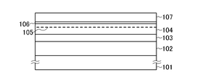
- FIG. 2A is a cross-sectional view showing a state of a semiconductor device in an intermediate process for explaining a method for manufacturing a semiconductor device according to an embodiment of the present invention.
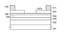
- FIG. 2B is a cross-sectional view showing a state of the semiconductor device in the intermediate process for explaining the manufacturing method of the semiconductor device according to the embodiment of the present invention.
- FIG. 2C is a cross-sectional view showing a state of the semiconductor device in the intermediate process for explaining the manufacturing method of the semiconductor device according to the embodiment of the present invention.
- FIG. 2A is a cross-sectional view showing a state of a semiconductor device in an intermediate process for explaining a method for manufacturing a semiconductor device according to an embodiment of the present invention.
- FIG. 2B is a cross-sectional view showing a state of the semiconductor device in the intermediate process for explaining the manufacturing method of the semiconductor device according to the embodiment of the present invention
- FIG. 2D is a cross-sectional view showing a state of the semiconductor device in the intermediate process for explaining the manufacturing method of the semiconductor device according to the embodiment of the present invention.
- FIG. 2E is a cross-sectional view showing a state of the semiconductor device in the intermediate process for explaining the method for manufacturing the semiconductor device according to the embodiment of the present invention.
- FIG. 1 shows a cross section parallel to the gate length direction.
- This semiconductor device is a field effect transistor, and is a buffer layer 102, a channel layer 103, a barrier layer 104, a carrier supply layer 105, a gate electrode 108, a source electrode 110, and a drain electrode formed on the semiconductor substrate 101. It is equipped with 111.
- the buffer layer 102, the channel layer 103, and the barrier layer 104 are laminated in this order on the semiconductor substrate 101.
- the stacking order of the channel layer 103 and the barrier layer 104 is not limited to the above-mentioned configuration.
- the semiconductor substrate 101 is composed of, for example, a semi-insulating InP.
- the buffer layer 102 is composed of, for example, InAlAs, and has a layer thickness of 100 to 300 nm.
- the channel layer 103 is made of, for example, InGaAs, and has a layer thickness of 5 to 20 nm.
- the barrier layer 104 is composed of, for example, InAlAs, and has a layer thickness of 5 to 20 nm.
- the carrier supply layer 105 is formed on the barrier layer 104 by, for example, a well-known sheet doping, and is doped with Si as an impurity by 1 ⁇ 10 19 cm -3 .
- the stopper layer 106 is provided on the barrier layer 104.
- the stopper layer 106 is composed of, for example, InP, and has a layer thickness of 2 to 5 nm. These can be formed by crystal growth, for example, by a metalorganic vapor phase growth method, a molecular beam epitaxy method, or the like.
- This semiconductor device includes a recess 104a formed halfway in the thickness direction in the barrier layer 104.
- the recess 104a is a groove extending in the gate width direction.
- the gate electrode 108 is partially penetrated into the recess 104a and formed on the barrier layer 104.
- the gate electrode 108 has a T-shaped cross-sectional view, and is formed continuously on the penetration portion 108a and the penetration portion 108a penetrating into the recess 104a, and the leg portions 108b and the leg portions 108b having a short length in the gate length direction. It comprises a head 108c that is continuously formed on top and whose length in the gate length direction is longer than the leg 108b.
- the gate electrode 108 can be made of, for example, platinum or gold.
- the source electrode 110 and the drain electrode 111 are formed on the barrier layer 104 with the gate electrode 108 interposed therebetween.
- the source electrode 110 and the drain electrode 111 can be composed of, for example, Ti / Pt / Au.
- a cap layer 107 is formed between the source electrode 110 and the drain electrode 111 and the barrier layer 104.
- the cap layer 107 is composed of, for example, InGaAs in which Si is doped in 1 ⁇ 10 19 to 2 ⁇ 10 19 cm -3.
- An opening 107a is formed in the cap layer 107.
- a gate electrode 108 is arranged in the opening 107a.
- the semiconductor device includes a gate insulating layer 109 between the bottom and side surfaces of the recess 104a and the gate electrode 108 (penetration portion 108a).
- the gate insulating layer 109 is composed of an oxide of a substance constituting the barrier layer 104.
- the gate insulating layer 109 is composed of, for example, an In oxide layer and an Al oxide layer.
- the gate insulating layer 109 is used.
- FIGS. 2A to 2E show cross sections parallel to the gate length direction.
- a buffer layer 102, a channel layer 103, a barrier layer 104, a carrier supply layer 105, and a cap layer 107 are formed on the semiconductor substrate 101 (first step).
- the buffer layer 102, the channel layer 103, the barrier layer 104, and the cap layer 107 are sequentially laminated on the semiconductor substrate 101 by crystal growth by a metalorganic vapor phase growth method, a molecular beam epitaxy method, or the like.
- a carrier supply layer 105 is formed on the barrier layer 104 by sheet doping.
- the stopper layer 106 is formed between the carrier supply layer 105 and the cap layer 107.
- a mesa region is formed by patterning by wet etching or dry etching.
- the source electrode 110 and the drain electrode 111 are formed on the cap layer 107 so as to be separated from each other (second step).
- the source electrode 110 and the drain electrode 111 are formed so as to sandwich the region forming the gate electrode 108.
- Ti / Pt / Au is deposited on the cap layer 107 to form a metal film, and the metal film is patterned by a known photolithography technique and etching technique to obtain a source electrode 110 and a drain electrode 111.
- Form It is also possible to form the source electrode 110 and the drain electrode 111 by a known lift-off method.
- the source electrode 110 and the drain electrode 111 are ohmic-bonded to the cap layer 107.
- an opening 107a penetrating the cap layer 107 is formed in the cap layer 107 (third step).
- the opening 107a is formed by patterning the cap layer 107 by a known lithography technique and etching technique.
- the opening 107a is formed by selectively etching the cap layer 107 by wet etching using an etching solution such as citric acid or phosphoric acid as an etchant using a mask pattern (not shown) made of an insulating material or a resist. Can be formed.
- the stopper layer 106 made of InP is hardly etched by the above-mentioned etching solution, becomes an etching stop layer (stopper layer), and can prevent the barrier layer 104 from being etched.
- stopper layer 106 By using the stopper layer 106 in this way, etching with good controllability in the depth (thickness) direction can be performed.
- the source electrode 110 and the drain electrode 111 may be formed after the opening 107a is formed, and the order of manufacturing these is within the scope of studying the transistor manufacturing process.
- a recess 104a is formed in the barrier layer 104 in the region of the opening 107a halfway in the thickness direction (fourth step).
- the recess 104a is formed through the stopper layer 106 and halfway in the thickness direction of the barrier layer 104.
- the depth of the recess 104a is set within a range that exceeds the thickness of the stopper layer 106 and does not exceed the sum of the thicknesses of the stopper layer 106 and the barrier layer 104.
- the depth of the recess 104a is set in the range of 5 nm to 20 nm.
- the recess 104a can be formed, for example, by an etching process of forming an oxide layer by oxidation from the surface side and removing the oxide layer. For example, using a mask pattern (not shown) having an opening in the region forming the recess 104a, the stopper layer 106 and the barrier layer 104 are selectively oxidized from the surface side, and the oxide layer formed by this oxidation is wet-etched. Selectively remove.
- the above-mentioned formation of the oxide layer and removal of the oxide layer are carried out by alternately immersing the hydrogen peroxide-based solution (oxidation process) and the citric acid or phosphoric acid-based etchant (etching process).
- oxidation process a very thin oxide layer with a thickness of sub-nanometer is formed on the exposed surface of the layer to be etched, and in the etching process, the very thin oxide layer is removed.
- the recess 104a can also be formed by well-known atomic layer etching.
- atomic layer etching for example, a chemical modification process for the outermost surface of the atomic layer using chlorine gas plasma and an etching process for the chemical modification layer using argon gas plasma are alternately performed using a predetermined plasma processing device. conduct. Also in this etching processing method, it is possible to precisely control the etching amount by the number of repetitions of the two processes.
- a gate insulating layer 109 composed of an oxide of a substance constituting the barrier layer 104 is formed (fifth). Process).
- the formation of the gate insulating layer 109 by oxidizing the barrier layer 104 can be carried out, for example, by a wet treatment using a solution containing an oxidizing agent.
- constituent substances such as In and Al are locally oxidized with an oxidizing agent such as hydrogen peroxide.
- This wet treatment (fifth step) is continuously performed in the formation of the recess 104a (fourth step) described above, and after the wet etching in the recess 104a, the gate insulating layer 109 is provided without drying the treated portion. Can be formed.
- the oxidation process with a solution of hydrogen peroxide and the etching process with a citric acid or phosphoric acid-based etchant are alternately performed to form the recess 104a, and subsequently, the recess 104a is formed.
- Oxidation is carried out by an oxidation process with a solution of hydrogen peroxide.
- the formation of the recess 104a and the formation of the gate insulating layer 109 can be continuously performed, and the treatment target portion is not dried. Therefore, a good interface between the semiconductor and the oxide layer with few interface defects. Can be formed.
- the gate insulating layer 109 formed by oxidizing the barrier layer 104 and composed of the above-mentioned oxide has a high dielectric constant and a band gap, and is a layer having a high barrier for electrons. As a result, a good MOS structure can be formed by using the gate insulating layer 109.
- the gate insulating layer 109 formed by the above-mentioned wet treatment is composed of an In oxide layer and an Al oxide layer.
- InAlAs is etched with citric acid, In 2 O 3 segregates on the surface side (gate electrode side) under this condition, and Al 2 O 3 and indium / Al oxide are formed on the inner side (channel layer side). Will be done.
- a gate insulating layer 109 composed of two or more constituents having a high band gap at the interface with the semiconductor and having a high dielectric constant effective for suppressing the short channel effect by concentrating an electric field on the gate electrode side is provided. You will be able to form.
- the gate insulating layer 109 can be composed of a two-layer structure or more of an In oxide layer and an Al oxide layer, and the constituents of each layer are In oxide, Al oxide, or these. It is composed of mixed oxides.
- the thickness of the gate insulating layer 109 formed by the above-mentioned wet treatment can be accurately controlled according to the "Luke's model" depending on the immersion time in the treatment liquid and the temperature of the treatment liquid, and is 0.5 to 5 nm. It can be formed in any thickness of the range with good controllability.
- the thickness of the gate insulating layer 109 is formed within a range not exceeding 1/2 of the sum of the thicknesses of the stopper layer 106 and the barrier layer 104.
- the thickness of the gate insulating layer 109 can be 10 nm or less, typically about 2 nm, which is 1/10 of the thickness.
- the formation of the gate insulating layer 109 (fifth step) by oxidation of the barrier layer 104 can also be carried out by, for example, a dry treatment using plasma with a gas containing oxygen.
- the gate insulating layer 109 can be formed without releasing the processing atmosphere to the atmosphere during this processing, and the quality is particularly high. It is possible to obtain a good interface between the semiconductor and the insulating layer.
- a recess 104a is formed by atomic layer etching in a closed and depressurized processing atmosphere using a well-known processing device that performs atomic layer etching (4th step). For example, using a predetermined treatment device, a chemical modification process for the outermost surface of the atomic layer using chlorine gas plasma and an etching process for the chemical modification layer using argon gas plasma are alternately performed to form the recess 104a. do. Following this atomic layer etching, oxygen gas is introduced into the treatment chamber without releasing the treatment atmosphere (treatment chamber) to the atmosphere, and plasma of the introduced oxygen gas is generated. By acting the plasma of the generated oxygen gas, the barrier layer 104 of the portion exposed on the side surface and the bottom surface of the recess 104a is oxidized to form the gate insulating layer 109.
- the treatment target Before introducing oxygen gas into the treatment chamber, the treatment target is heated under a low vacuum to selectively remove As, which has a high vapor pressure with respect to other constituent elements, and then the above-mentioned oxygen.
- the gate insulating layer 109 can also be formed by oxidizing In and Al using plasma. Even in the formation of the gate insulating layer 109 by this dry treatment, the thickness can be accurately controlled by the power of the oxygen plasma and the sample temperature, as in the case of the wet treatment described above.
- the gate electrode 108 is formed by partially penetrating into the recess 104a in which the gate insulating layer 109 is formed and arranged on the barrier layer 104 (sixth). Process). As a result, the field effect transistor shown in FIG. 1 can be obtained.
- a mask pattern having an opening at a position where the gate electrode 108 is formed is used, and the gate insulating layer 109 is formed without removing the mask pattern.
- the gate electrode material is deposited by, for example, a sputtering method in a state where the mask pattern is formed. After that, if the mask pattern is removed (lifted off), the gate electrode 108 can be formed.
- the gate insulating layer 109 when the gate insulating layer 109 is formed by dry treatment, the volume of the gate electrode material described above can be carried out while maintaining the vacuum state of the processing chamber in which the gate insulating layer 109 is formed.
- the gate electrode 108 By forming the gate electrode 108 in this way, the surface of the gate insulating layer 109 does not come into contact with the atmosphere. As a result, it is possible to prevent contamination from adhering to the surface of the gate insulating layer 109 due to contact with the atmosphere. As a result, defects at the interface between the gate electrode 108 and the gate insulating layer 109 can be reduced, which is advantageous for improving the characteristics.
- the gate insulating layer composed of the oxide of the substance constituting the barrier layer is used, a MOS type field effect transistor having good characteristics can be manufactured with high throughput. become able to.
- 101 semiconductor substrate, 102 ... buffer layer, 103 ... channel layer, 104 ... barrier layer, 104a ... recess, 105 ... carrier supply layer, 106 ... stopper layer, 107 ... cap layer, 108 ... gate electrode, 108a ... penetration portion, 108b ... legs, 108c ... head, 109 ... gate insulating layer, 110 ... source electrode, 111 ... drain electrode.
Landscapes
- Junction Field-Effect Transistors (AREA)
- Insulated Gate Type Field-Effect Transistor (AREA)
- Electrodes Of Semiconductors (AREA)
- Engineering & Computer Science (AREA)
- Manufacturing & Machinery (AREA)
Abstract
半導体装置(電界効果型トランジスタ)は、凹部(104a)の底部および側面とゲート電極(108)の貫入部(108a)との間に、ゲート絶縁層(109)を備える。ゲート絶縁層(109)は、障壁層(104)を構成する物質の酸化物から構成されたている。ゲート絶縁層(109)は、例えば、In酸化物の層およびAl酸化物の層から構成されている。
Description
本発明は、化合物半導体から構成された半導体装置およびその製造方法に関する。
0.3~3.0THzの電磁波周波数帯であるテラヘルツ波の性質には、数10Gb/sを超える高速無線通信や、3次元イメージングによる非破壊内部検査、電磁波吸収を利用した成分分析など、これまでにはない新たなアプリケーション創出の可能性が秘められている。
テラヘルツ波によるアプリケーションを実現する場合には、これを構成する電子デバイスにもより良好な高周波特性が必要とされる。一般的に、良好な高周波特性を有する電子デバイスとして、物性的に特に高い電子移動度を有する化合物半導体を材料とした電界効果型トランジスタが用いられる。
上述した電界効果型トランジスタは、半導体基板と、半導体基板の上に形成される半導体積層構造と、半導体積層構造の表面に形成されるゲート電極、およびゲート電極の両脇に形成されるソース電極、ドレイン電極から構成される。特に、高周波特性に優れる高電子移動度トランジスタは、半導体基板の側から、バッファ層、チャネル層、障壁層、ストッパ層、キャップ層、パッシベーション層が順次に積層されて構成されている。また、キャリア供給層が、チャネル層に対して障壁層側もしくはチャネル層に対してバッファ層側に形成される。この構成において、素子特性の設計に応じて、キャリア供給層の位置や不純物のドープ量が設計される。
この種の電界効果型トランジスタでは、ゲート電極に対して電位を印加すると、印加した電位の強度に応じ、キャリア供給層からチャネル層に対してキャリアが供給されて形成される2次元電子ガスの濃度が変調され、ソース電極、ドレイン電極間に形成された伝導チャネルを通じて電子が移動する。この電子(キャリア)が移動(走行)する伝導チャネルが形成されるチャネル層とキャリア供給層とは、空間的に分離され、キャリア供給層における不純物による散乱が抑制される。このため、上述した電界効果型トランジスタでは、電子移動度を向上させることができ、高周波動作を実現することができる。
電界効果型トランジスタの高周波特性を向上させるためには,短チャネル効果の抑制が重要であり、ゲート電極とチャネルとの間の距離を短縮することが有効である。しかしゲート電極とチャネルとの間の距離を単純に短縮するだけでは、ゲート電極の電子からみた障壁の厚さが薄くなり、電子のトンネリングが生じてゲート電極からの漏れ電流が増加する。
この問題に対処するため、ゲート電極と障壁層との間に高い障壁高さを有するゲート酸化層を形成し、MOS型の電界効果型トランジスタとする方法が一般的である。ゲート絶縁層を、障壁層に比べ高誘電率の材料から構成し、実効的なゲート絶縁層の厚さを薄くしている。非特許文献1に記載された技術では、ウエット処理によって障壁層のエッチングを高い精度で実施し、ゲート電極と障壁層との間の距離を短縮している。この技術では、障壁層のエッチング処理に引き続いて、原子層堆積法により高い誘電率を有する材料を堆積してゲート絶縁層を形成している。非特許文献1に記載された技術では、上述したことにより、良好な特性を有するMOS型電界効果型トランジスタを実現している。
J. Lin et al., "A Novel Digital Etch Technique for Deeply Scaled III-V MOSFETs", IEEE Electron Device Letters, vol. 35, no. 4, pp. 440-442, 2014.
しかしながら、上述した技術では、ゲート絶縁層の形成に原子層堆積法を適用していることから、製造工程のスループットが低下する。原子層堆積法では,堆積対象表面の水和化と、プリカーサ導入による酸化とを交互に繰り返し、原子層単位で酸化層を形成する技術である。このため、目的の膜厚を有するゲート絶縁層を形成するためには、上記のサイクルを相当数繰り返す必要があり、製造にかかるスループットが低下する。このように、従来の技術では、良好な特性を有するMOS型電界効果型トランジスタが、高いスループットで製造することができないという問題があった。
本発明は、以上のような問題点を解消するためになされたものであり、良好な特性を有するMOS型電界効果型トランジスタが、高いスループットで製造できるようにすることを目的とする。
本発明に係る半導体装置は、半導体基板の上に形成された、バッファ層、チャネル層、障壁層、キャリア供給層と、障壁層に、厚さ方向の途中まで形成された凹部と、凹部に一部が貫入して障壁層の上に形成されたゲート電極と、ゲート電極を挟んで障壁層の上に形成されたソース電極およびドレイン電極と、ソース電極およびドレイン電極と障壁層との間に形成されたキャップ層と、凹部の底部および側面とゲート電極との間に形成され、障壁層を構成する物質の酸化物から構成されたゲート絶縁層とを備える。
また、本発明に係る半導体装置の製造方法は、半導体基板の上に、バッファ層、チャネル層、障壁層、キャリア供給層、キャップ層が形成された状態とする第1工程と、キャップ層の上に、互いに離間してソース電極およびドレイン電極を形成する第2工程と、ソース電極とドレイン電極との間のゲート形成領域のキャップ層に、キャップ層を貫通する開口を形成する第3工程と、開口の領域内の障壁層に、厚さ方向の途中まで凹部を形成する第4工程と、凹部の底部および側面の障壁層を酸化することで、障壁層を構成する物質の酸化物から構成されたゲート絶縁層を形成する第5工程と、ゲート絶縁層が形成された凹部に、一部が貫入して障壁層の上に配置されたゲート電極を形成する第6工程とを備える。
以上説明したように、本発明によれば、障壁層を構成する物質の酸化物から構成されたゲート絶縁層を用いるので、良好な特性を有するMOS型電界効果型トランジスタが、高いスループットで製造できるようになる。
以下、本発明の実施の形態に係る半導体装置について図1を参照して説明する。なお、図1は、ゲート長方向に平行な断面を示している。この半導体装置は、電界効果型トランジスタであり、半導体基板101の上に形成された、バッファ層102、チャネル層103、障壁層104、キャリア供給層105、ゲート電極108、ソース電極110、およびドレイン電極111を備える。なお、実施の形態では、半導体基板101の上に、バッファ層102、チャネル層103、障壁層104が、これらの順に積層されている。なお、チャネル層103、障壁層104の積層順は、上述した構成に限るものではない。
半導体基板101は、例えば半絶縁性のInPから構成されている。バッファ層102は、例えば、InAlAsから構成され、層厚100~300nmとされている。チャネル層103は、例えば、InGaAsから構成され、層厚5~20nmとされている。障壁層104は、例えば、InAlAsから構成され、層厚5~20nmとされている。キャリア供給層105は、例えば、よく知られたシートドープにより、障壁層104に形成され、不純物としてSiが1×1019cm-3ドープされている。実施の形態では、障壁層104の上に、ストッパ層106を備える。ストッパ層106は、例えば、InPから構成され、層厚2~5nmとされている。これらは、例えば、有機金属気相成長法や分子線エピタキシー法などにより結晶成長することで形成できる。
この半導体装置は、障壁層104に、厚さ方向の途中まで形成された凹部104aを備える。凹部104aは、ゲート幅方向に延在する溝である。ゲート電極108は、凹部104aに、一部が貫入して障壁層104の上に形成されている。ゲート電極108は、断面視T字型とされ、凹部104aに貫入した貫入部108a、貫入部108aの上に連続して形成され、ゲート長方向の長さが短い脚部108b、脚部108bの上に連続して形成され、ゲート長方向の長さが脚部108bより長い頭部108cを備える。ゲート電極108は、例えば、白金や金から構成することができる。
ソース電極110およびドレイン電極111は、ゲート電極108を挟んで障壁層104の上に形成されている。ソース電極110およびドレイン電極111は、例えば、Ti/Pt/Auから構成することができる。また、ソース電極110およびドレイン電極111と障壁層104との間には、キャップ層107が形成されている。キャップ層107は、例えば、Siが1×1019~2×1019cm-3にドープされたInGaAsから構成されている。キャップ層107には、開口107aが形成されている。開口107aに、ゲート電極108が配置されている。
また、実施の形態に係る半導体装置(電界効果型トランジスタ)は、凹部104aの底部および側面とゲート電極108(貫入部108a)との間に、ゲート絶縁層109を備える。ゲート絶縁層109は、障壁層104を構成する物質の酸化物から構成されたている。ゲート絶縁層109は、例えば、In酸化物の層およびAl酸化物の層から構成されている。
ゲート電極108とチャネルとの間隔を単純に短縮した状態では,ゲート電極108の電子からみた障壁層104の厚さが薄くなり,電子のトンネリングが生じてゲート電極108からの漏れ電流が増加する。この問題を回避するために,ゲート絶縁層109を用いる。
次に、本発明の実施の形態に係る半導体装置(電界効果型トランジスタ)の製造方法について、図2A~図2Eを参照して説明する。なお、図2A~図2Eは、ゲート長方向に平行な断面を示している。
まず、図2Aに示すように、半導体基板101の上に、バッファ層102、チャネル層103、障壁層104、キャリア供給層105、キャップ層107を形成する(第1工程)。
例えば、半導体基板101の上に、バッファ層102,チャネル層103,障壁層104,キャップ層107を有機金属気相成長法や分子線エピタキシー法などにより結晶成長することで順次積層する。また、障壁層104には、シートドープによりキャリア供給層105を形成する。また、実施の形態では、キャリア供給層105とキャップ層107との間にストッパ層106を形成する。また、素子間分離のために、ウエットエッチングまたはドライエッチングによるパターニングで、メサ領域を形成する。
次に、図2Bに示すように、キャップ層107の上に、互いに離間してソース電極110およびドレイン電極111を形成する(第2工程)。ソース電極110およびドレイン電極111は、ゲート電極108を形成する領域を挟んで形成する。例えば、キャップ層107上に、Ti/Pt/Auを堆積して金属膜を形成し、この金属膜を公知のフォトリソグラフィ技術とエッチング技術とによりパターニングすることで、ソース電極110およびドレイン電極111を形成する。また、公知のリフトオフ法により、ソース電極110およびドレイン電極111を形成することも可能である。ソース電極110,ドレイン電極111は、キャップ層107にオーミック接合する。
次に、図2Cに示すように、キャップ層107に、キャップ層107を貫通する開口107aを形成する(第3工程)。公知のリソグラフィ技術とエッチング技術とによりキャップ層107をパターニングすることで、開口107aを形成する。
例えば、絶縁材料やレジストなどによるマスクパターン(不図示)を用い、クエン酸やリン酸などによるエッチング液をエッチャントとして用いたウエットエッチングにより、キャップ層107を選択的にエッチングすることで、開口107aが形成できる。このエッチングにおいて、InPからなるストッパ層106は、上述したエッチング液ではほとんどエッチングされず、エッチングの停止層(ストッパ層)となり、障壁層104がエッチングされることを防ぐことができる。このようにストッパ層106を用いることで、深さ(厚さ)方向に対して制御性のよいエッチングができる。なお、ソース電極110およびドレイン電極111は、開口107aを形成した後に形成してもよく、これらの作製の順序は、トランジスタ作製工程検討の範囲内である。
次に、図2Dに示すように、開口107aの領域内の障壁層104に、厚さ方向の途中まで凹部104aを形成する(第4工程)。実施の形態では、ストッパ層106を形成しているので、ストッパ層106を貫通し、障壁層104の厚さ方向の途中まで、凹部104aを形成する。凹部104aの深さは,ストッパ層106の厚さを超え、ストッパ層106と障壁層104との厚さの和を超えない範囲で設定される。例えば、典型的には、ストッパ層106の厚さが5nm,ストッパ層106と障壁層104の厚さの和が20nmの場合,凹部104aの深さは5nm~20nmの範囲で設定される。
凹部104aは、例えば、表面側からの酸化による酸化層の形成と酸化層の除去とによるエッチング処理で形成することができる。例えば、凹部104aを形成する領域に開口を有するマスクパターン(不図示)を用い、ストッパ層106および障壁層104を表面側から選択的に酸化し、この酸化により形成された酸化層をウエットエッチングにより選択的に除去する。
例えば、過酸化水素系の溶液(酸化プロセス)と、クエン酸やリン酸系のエッチャント(エッチングプロセス)とに、交互に浸漬させることで、上述した酸化層の形成と酸化層の除去とが実施できる。酸化プロセスでは、エッチング対象の層の露出している表面に、サブナノメートルの厚さのごく薄い酸化層を形成し、エッチングプロセスでは、ごく薄い酸化層を除去するものであり、浸漬(処理)時間ではなく、2つのプロセスの繰り返し回数でエッチング量を精密に制御することが可能である。
また、凹部104aは、よく知られた原子層エッチングにより形成することもできる。原子層エッチングでは、例えば、所定のプラズマ処理装置を用い、塩素ガスのプラズマを用いた原子層最表面に対する化学修飾プロセスと、アルゴンガスのプラズマを用いた、化学修飾層のエッチングプロセスとを交互に行う。このエッチング処理方法においても、2つのプロセスの繰り返し回数でエッチング量を精密に制御することが可能である。
次に、図2Eに示すように、凹部104aの底部および側面の障壁層104を酸化することで、障壁層104を構成する物質の酸化物から構成されたゲート絶縁層109を形成する(第5工程)。
障壁層104の酸化によるゲート絶縁層109の形成は、例えば、酸化剤を含む溶液を用いたウエット処理により実施できる。ウエット処理では,例えば過酸化水素などの酸化剤により,InやAlなどの構成物質を局所的に酸化する。このウエット処理(第5工程)は、前述した凹部104aの形成(第4工程)に連続して実施し、凹部104aにおけるウエットエッチングの後で、処理対象箇所を乾燥させることなくゲート絶縁層109を形成することができる。
前述したように、凹部104aの形成において、過酸化水素の溶液による酸化プロセスと、クエン酸やリン酸系のエッチャントによるエッチングプロセスとを交互に実施して凹部104aを形成し、これに続いて、過酸化水素の溶液による酸化プロセスで酸化を実施する。この処理では、凹部104aの形成と、ゲート絶縁層109の形成とを、連続して実施でき、処理対象箇所を乾燥させることがないので、界面欠陥の少ない、良好な半導体と酸化層との界面を形成することができる。
ここで、障壁層104を構成するInAlAsを酸化することで、In、Al、Asの各々の酸化物が形成される。酸化インジウム(In2O3)は、誘電率が10~20と比較的高くそのバンドギャップも2.5~3.5eVと比較的高い。また酸化アルミニウム(Al2O3)は、誘電率が10程度ではあるが、バンドギャップは6~9eVと非常に高い。従って、障壁層104を酸化することで形成され、上述した酸化物から構成されるゲート絶縁層109は、高い誘電率およびバンドギャップを有するものとなり、電子にとって障壁の高い層となる。この結果、ゲート絶縁層109を用いることで、良好なMOS構造を形成することができる。
上述したウエット処理により形成されるゲート絶縁層109は、In酸化物の層およびAl酸化物の層から構成されるものとなる。例えば、クエン酸によってInAlAsをエッチングすると、この条件により、In2O3が表面側(ゲート電極側)に偏析し,Al2O3やインジウム・Al酸化物が、内側(チャネル層側)に形成されるようになる。この場合、半導体との界面で高いバンドギャップを有し、かつゲート電極側には電界を集中させ短チャネル効果抑制に有効な高誘電率を有する2層以上の構成成分からなるゲート絶縁層109を形成することができるようになる。このように、ゲート絶縁層109は、In酸化物の層とAl酸化物の層との2層構造以上から構成することができ、各層の構成成分はIn酸化物またはAl酸化物、もしくはこれらが混合した酸化物から構成されたものとなる。
上述したウエット処理により形成するゲート絶縁層109の厚さは、処理液に対する浸漬時間や、処理液の温度によって、「Luke's model」に従った正確な制御が可能であり、0.5~5nmの範囲のいずれかの厚さに、制御性よく形成することができる。
ゲート絶縁層109の厚さは、ストッパ層106と障壁層104との厚さの和の1/2を超えない範囲で形成する。例えば、ストッパ層106と障壁層104の厚さの和が20nmの場合、ゲート絶縁層109の厚さは10nm以下,典型的には1/10の厚さとなる2nm程度とすることができる。
また、障壁層104の酸化によるゲート絶縁層109の形成(第5工程)は、例えば、酸素を含むガスによるプラズマを用いたドライ処理により実施することもできる。この場合、凹部104aの形成(第4工程)を、原子層エッチングにより実施することで、この処理時引き続き、処理雰囲気を大気解放することなく、ゲート絶縁層109を形成することができ、特に品質の良い半導体と絶縁層の界面を得ることができる。
まず、よく知られた原子層エッチングを実施する処理装置を用い、密閉されて減圧された処理雰囲気における原子層エッチングにより凹部104aを形成する(第4工程)。例えば、所定の処理装置を用い、塩素ガスのプラズマを用いた原子層最表面に対する化学修飾プロセスと、アルゴンガスのプラズマを用いた、化学修飾層のエッチングプロセスとを交互に行い、凹部104aを形成する。この原子層エッチングに引き続き、処理雰囲気(処理室)を大気解放することなく、処理室に酸素ガスを導入し、導入した酸素ガスのプラズマを生成する。生成した酸素ガスのプラズマを作用させることで、凹部104aの側面および底面に露出している部分の障壁層104を酸化し、ゲート絶縁層109を形成する。
なお、処理室内に酸素ガスを導入する前に、低真空下で処置対象を加熱し、他の構成元素に対して蒸気圧の高いAsを昇華させることで選択に除去してから、上述した酸素プラズマを用いてInおよびAlを酸化させることで、ゲート絶縁層109を形成することもできる。このドライ処理によるゲート絶縁層109の形成においても、前述したウエット処理の場合と同様に、酸素プラズマのパワーや試料温度によって、厚さを正確に制御することができる。
以上のようにしてゲート絶縁層109を形成した後、ゲート絶縁層109が形成された凹部104aに、一部が貫入して障壁層104の上に配置されたゲート電極108を形成する(第6工程)。これにより、図1に示す電界効果型トランジスタが得られる。例えば、凹部104aの形成において、ゲート電極108を形成する箇所に開口を有するマスクパターンを用い、このマスクパターンを除去することなくゲート絶縁層109を形成する。ゲート絶縁層109を形成した後、上記マスクパターンが形成されている状態で、ゲート電極材料を、例えば、スパッタ法などにより堆積する。この後、マスクパターンを除去(リフトオフ)すれば、ゲート電極108を形成することができる。
例えば、ドライ処理によりゲート絶縁層109を形成する場合、ゲート絶縁層109を形成した処理室の真空状態を維持しながら、上述したゲート電極材料の体積を実施することができる。このようにしてゲート電極108を形成することで、ゲート絶縁層109の表面が、大気に触れることが無い。この結果、大気に触れることなどによる、ゲート絶縁層109の表面に対するコンタミネーションの付着などが防止できる。この結果、ゲート電極108とゲート絶縁層109との界面の欠陥を低減することができ,特性改善に有利に作用する。
以上に説明したように、本発明によれば、障壁層を構成する物質の酸化物から構成されたゲート絶縁層を用いるので、良好な特性を有するMOS型電界効果型トランジスタが、高いスループットで製造できるようになる。
なお、本発明は以上に説明した実施の形態に限定されるものではなく、本発明の技術的思想内で、当分野において通常の知識を有する者により、多くの変形および組み合わせが実施可能であることは明白である。
101…半導体基板、102…バッファ層、103…チャネル層、104…障壁層、104a…凹部、105…キャリア供給層、106…ストッパ層、107…キャップ層、108…ゲート電極、108a…貫入部、108b…脚部、108c…頭部、109…ゲート絶縁層、110…ソース電極、111…ドレイン電極。
Claims (8)
- 半導体基板の上に形成された、バッファ層、チャネル層、障壁層、キャリア供給層と、
前記障壁層に、厚さ方向の途中まで形成された凹部と、
前記凹部に一部が貫入して前記障壁層の上に形成されたゲート電極と、
前記ゲート電極を挟んで前記障壁層の上に形成されたソース電極およびドレイン電極と、
前記ソース電極および前記ドレイン電極と前記障壁層との間に形成されたキャップ層と、
前記凹部の底部および側面と前記ゲート電極との間に形成され、前記障壁層を構成する物質の酸化物から構成されたゲート絶縁層と
を備える半導体装置。 - 請求項1記載の半導体装置において、
前記障壁層は、InAlAsから構成されてることを特徴とする半導体装置。 - 請求項2記載の半導体装置において、
ゲート絶縁層は、In酸化物の層およびAl酸化物の層から構成されていることを特徴とする半導体装置。 - 半導体基板の上に、バッファ層、チャネル層、障壁層、キャリア供給層、キャップ層が形成された状態とする第1工程と、
前記キャップ層の上に、互いに離間してソース電極およびドレイン電極を形成する第2工程と、
前記ソース電極と前記ドレイン電極との間のゲート形成領域の前記キャップ層に、前記キャップ層を貫通する開口を形成する第3工程と、
前記開口の領域内の前記障壁層に、厚さ方向の途中まで凹部を形成する第4工程と、
前記凹部の底部および側面の前記障壁層を酸化することで、前記障壁層を構成する物質の酸化物から構成されたゲート絶縁層を形成する第5工程と、
前記ゲート絶縁層が形成された前記凹部に、一部が貫入して前記障壁層の上に配置されたゲート電極を形成する第6工程と
を備える半導体装置の製造方法。 - 請求項4記載の半導体装置の製造方法において、
前記第5工程は、酸化剤を含む溶液を用いたウエット処理により前記ゲート絶縁層を形成する
ことを特徴とする半導体装置の製造方法。 - 請求項5記載の半導体装置の製造方法において、
前記第4工程は、ウエットエッチングにより前記凹部を形成し、
前記第5工程は、前記第4工程におけるウエットエッチングの後で、処理対象箇所を乾燥させることなく前記ゲート絶縁層を形成する
ことを特徴とする半導体装置の製造方法。 - 請求項4記載の半導体装置の製造方法において、
前記第5工程は、酸素を含むガスによるプラズマを用いたドライ処理により前記ゲート絶縁層を形成する
ことを特徴とする半導体装置の製造方法。 - 請求項5記載の半導体装置の製造方法において、
前記第4工程は、密閉されて減圧された処理雰囲気における原子層エッチングにより前記凹部を形成し、
前記第5工程は、前記原子層エッチングに引き続き、処理雰囲気を大気解放することなく、前記ゲート絶縁層を形成する
ことを特徴とする半導体装置の製造方法。
Priority Applications (3)
| Application Number | Priority Date | Filing Date | Title |
|---|---|---|---|
| JP2022522090A JP7392842B2 (ja) | 2020-05-11 | 2020-05-11 | 半導体装置およびその製造方法 |
| US17/914,645 US20230117607A1 (en) | 2020-05-11 | 2020-05-11 | Semiconductor Device and Method of Manufacturing the Same |
| PCT/JP2020/018776 WO2021229629A1 (ja) | 2020-05-11 | 2020-05-11 | 半導体装置およびその製造方法 |
Applications Claiming Priority (1)
| Application Number | Priority Date | Filing Date | Title |
|---|---|---|---|
| PCT/JP2020/018776 WO2021229629A1 (ja) | 2020-05-11 | 2020-05-11 | 半導体装置およびその製造方法 |
Publications (1)
| Publication Number | Publication Date |
|---|---|
| WO2021229629A1 true WO2021229629A1 (ja) | 2021-11-18 |
Family
ID=78525425
Family Applications (1)
| Application Number | Title | Priority Date | Filing Date |
|---|---|---|---|
| PCT/JP2020/018776 Ceased WO2021229629A1 (ja) | 2020-05-11 | 2020-05-11 | 半導体装置およびその製造方法 |
Country Status (3)
| Country | Link |
|---|---|
| US (1) | US20230117607A1 (ja) |
| JP (1) | JP7392842B2 (ja) |
| WO (1) | WO2021229629A1 (ja) |
Citations (6)
| Publication number | Priority date | Publication date | Assignee | Title |
|---|---|---|---|---|
| JPH0992660A (ja) * | 1995-09-26 | 1997-04-04 | Matsushita Electron Corp | 電界効果トランジスタ及びその製造方法 |
| JPH10284466A (ja) * | 1997-02-04 | 1998-10-23 | Mitsubishi Electric Corp | エッチング方法,結晶成長方法,並びに半導体装置の製造方法 |
| JP2004311869A (ja) * | 2003-04-10 | 2004-11-04 | Mitsubishi Electric Corp | 窒化物半導体系電界効果トランジスタとその製造方法 |
| JP2005260172A (ja) * | 2004-03-15 | 2005-09-22 | Matsushita Electric Ind Co Ltd | 半導体装置及び半導体レーザ装置の製造方法 |
| JP2011049314A (ja) * | 2009-08-26 | 2011-03-10 | Asahi Kasei Electronics Co Ltd | 半導体装置およびその製造方法 |
| JP2013229499A (ja) * | 2012-04-26 | 2013-11-07 | Rohm Co Ltd | 窒化物半導体装置およびその製造方法 |
Family Cites Families (2)
| Publication number | Priority date | Publication date | Assignee | Title |
|---|---|---|---|---|
| US8012816B2 (en) * | 2008-12-31 | 2011-09-06 | Intel Corporation | Double pass formation of a deep quantum well in enhancement mode III-V devices |
| JP5913816B2 (ja) * | 2011-02-21 | 2016-04-27 | 富士通株式会社 | 半導体装置の製造方法 |
-
2020
- 2020-05-11 US US17/914,645 patent/US20230117607A1/en active Pending
- 2020-05-11 WO PCT/JP2020/018776 patent/WO2021229629A1/ja not_active Ceased
- 2020-05-11 JP JP2022522090A patent/JP7392842B2/ja active Active
Patent Citations (6)
| Publication number | Priority date | Publication date | Assignee | Title |
|---|---|---|---|---|
| JPH0992660A (ja) * | 1995-09-26 | 1997-04-04 | Matsushita Electron Corp | 電界効果トランジスタ及びその製造方法 |
| JPH10284466A (ja) * | 1997-02-04 | 1998-10-23 | Mitsubishi Electric Corp | エッチング方法,結晶成長方法,並びに半導体装置の製造方法 |
| JP2004311869A (ja) * | 2003-04-10 | 2004-11-04 | Mitsubishi Electric Corp | 窒化物半導体系電界効果トランジスタとその製造方法 |
| JP2005260172A (ja) * | 2004-03-15 | 2005-09-22 | Matsushita Electric Ind Co Ltd | 半導体装置及び半導体レーザ装置の製造方法 |
| JP2011049314A (ja) * | 2009-08-26 | 2011-03-10 | Asahi Kasei Electronics Co Ltd | 半導体装置およびその製造方法 |
| JP2013229499A (ja) * | 2012-04-26 | 2013-11-07 | Rohm Co Ltd | 窒化物半導体装置およびその製造方法 |
Also Published As
| Publication number | Publication date |
|---|---|
| US20230117607A1 (en) | 2023-04-20 |
| JPWO2021229629A1 (ja) | 2021-11-18 |
| JP7392842B2 (ja) | 2023-12-06 |
Similar Documents
| Publication | Publication Date | Title |
|---|---|---|
| CN106887454B (zh) | GaN基鳍栅增强型器件及其制作方法 | |
| CN111554742A (zh) | 一种GaN HEMT器件的制备方法 | |
| WO2021106190A1 (ja) | 電界効果型トランジスタおよびその製造方法 | |
| US9741859B2 (en) | Semiconductor device with graphene layer as channel | |
| JP7392842B2 (ja) | 半導体装置およびその製造方法 | |
| KR100450740B1 (ko) | 헤테로접합형 전계효과 트랜지스터 소자의 제조방법 | |
| CN107195670B (zh) | GaN基增强型MOS-HEMT器件及其制备方法 | |
| CN111430459B (zh) | AlGaAs/GaAs高电子迁移率晶体管及制备方法 | |
| JP6666168B2 (ja) | 電子装置およびその製造方法 | |
| CN115207094A (zh) | 半导体设备及其制造方法 | |
| JP2004119820A (ja) | 電界効果トランジスタおよびその製造方法 | |
| JP2018101755A (ja) | ヘテロ接合電界効果型トランジスタおよびその製造方法 | |
| JPH08321515A (ja) | 半導体装置とその製造方法 | |
| JP7632595B2 (ja) | 電界効果型トランジスタ | |
| JP5390487B2 (ja) | 電界効果トランジスタの製造方法 | |
| TWI438897B (zh) | The Method and Structure of Surface Oxidation Treatment of Nitride Heterogeneous Surface Field Effect Transistor by Hydrogen Peroxide | |
| US20150129890A1 (en) | Transistor | |
| CN113314416A (zh) | 一种GaN-HEMT器件上倾角结构的制备方法 | |
| JP5087235B2 (ja) | 窒化物半導体装置の製造方法 | |
| Cui et al. | Fmax= 270 GHz InAlN/GaN HEMT on Si with forming gas/nitrogen two-step annealing | |
| CN117747421B (zh) | 欧姆接触结构及其制备方法、GaN HEMT器件 | |
| JP6572556B2 (ja) | 化合物半導体装置及びその製造方法 | |
| JP2011049314A (ja) | 半導体装置およびその製造方法 | |
| JPH0951091A (ja) | 電界効果トランジスタ | |
| WO2026003911A1 (ja) | 半導体装置の製造方法 |
Legal Events
| Date | Code | Title | Description |
|---|---|---|---|
| 121 | Ep: the epo has been informed by wipo that ep was designated in this application |
Ref document number: 20935271 Country of ref document: EP Kind code of ref document: A1 |
|
| ENP | Entry into the national phase |
Ref document number: 2022522090 Country of ref document: JP Kind code of ref document: A |
|
| NENP | Non-entry into the national phase |
Ref country code: DE |
|
| 122 | Ep: pct application non-entry in european phase |
Ref document number: 20935271 Country of ref document: EP Kind code of ref document: A1 |