WO2021215145A1 - 基板処理装置及び基板処理方法 - Google Patents
基板処理装置及び基板処理方法 Download PDFInfo
- Publication number
- WO2021215145A1 WO2021215145A1 PCT/JP2021/010662 JP2021010662W WO2021215145A1 WO 2021215145 A1 WO2021215145 A1 WO 2021215145A1 JP 2021010662 W JP2021010662 W JP 2021010662W WO 2021215145 A1 WO2021215145 A1 WO 2021215145A1
- Authority
- WO
- WIPO (PCT)
- Prior art keywords
- substrate
- wafer
- height position
- height
- peripheral edge
- Prior art date
- Legal status (The legal status is an assumption and is not a legal conclusion. Google has not performed a legal analysis and makes no representation as to the accuracy of the status listed.)
- Ceased
Links
Images





Classifications
-
- H—ELECTRICITY
- H10—SEMICONDUCTOR DEVICES; ELECTRIC SOLID-STATE DEVICES NOT OTHERWISE PROVIDED FOR
- H10P—GENERIC PROCESSES OR APPARATUS FOR THE MANUFACTURE OR TREATMENT OF DEVICES COVERED BY CLASS H10
- H10P72/00—Handling or holding of wafers, substrates or devices during manufacture or treatment thereof
- H10P72/04—Apparatus for manufacture or treatment
- H10P72/0428—Apparatus for mechanical treatment or grinding or cutting
-
- B—PERFORMING OPERATIONS; TRANSPORTING
- B23—MACHINE TOOLS; METAL-WORKING NOT OTHERWISE PROVIDED FOR
- B23K—SOLDERING OR UNSOLDERING; WELDING; CLADDING OR PLATING BY SOLDERING OR WELDING; CUTTING BY APPLYING HEAT LOCALLY, e.g. FLAME CUTTING; WORKING BY LASER BEAM
- B23K26/00—Working by laser beam, e.g. welding, cutting or boring
- B23K26/50—Working by transmitting the laser beam through or within the workpiece
- B23K26/53—Working by transmitting the laser beam through or within the workpiece for modifying or reforming the material inside the workpiece, e.g. for producing break initiation cracks
-
- H—ELECTRICITY
- H10—SEMICONDUCTOR DEVICES; ELECTRIC SOLID-STATE DEVICES NOT OTHERWISE PROVIDED FOR
- H10P—GENERIC PROCESSES OR APPARATUS FOR THE MANUFACTURE OR TREATMENT OF DEVICES COVERED BY CLASS H10
- H10P52/00—Grinding, lapping or polishing of wafers, substrates or parts of devices
-
- H—ELECTRICITY
- H10—SEMICONDUCTOR DEVICES; ELECTRIC SOLID-STATE DEVICES NOT OTHERWISE PROVIDED FOR
- H10P—GENERIC PROCESSES OR APPARATUS FOR THE MANUFACTURE OR TREATMENT OF DEVICES COVERED BY CLASS H10
- H10P72/00—Handling or holding of wafers, substrates or devices during manufacture or treatment thereof
- H10P72/06—Apparatus for monitoring, sorting, marking, testing or measuring
- H10P72/0606—Position monitoring, e.g. misposition detection or presence detection
-
- H—ELECTRICITY
- H10—SEMICONDUCTOR DEVICES; ELECTRIC SOLID-STATE DEVICES NOT OTHERWISE PROVIDED FOR
- H10P—GENERIC PROCESSES OR APPARATUS FOR THE MANUFACTURE OR TREATMENT OF DEVICES COVERED BY CLASS H10
- H10P72/00—Handling or holding of wafers, substrates or devices during manufacture or treatment thereof
- H10P72/50—Handling or holding of wafers, substrates or devices during manufacture or treatment thereof for positioning, orientation or alignment
-
- H—ELECTRICITY
- H10—SEMICONDUCTOR DEVICES; ELECTRIC SOLID-STATE DEVICES NOT OTHERWISE PROVIDED FOR
- H10P—GENERIC PROCESSES OR APPARATUS FOR THE MANUFACTURE OR TREATMENT OF DEVICES COVERED BY CLASS H10
- H10P72/00—Handling or holding of wafers, substrates or devices during manufacture or treatment thereof
- H10P72/70—Handling or holding of wafers, substrates or devices during manufacture or treatment thereof for supporting or gripping
- H10P72/78—Handling or holding of wafers, substrates or devices during manufacture or treatment thereof for supporting or gripping using vacuum or suction, e.g. Bernoulli chucks
-
- H—ELECTRICITY
- H10—SEMICONDUCTOR DEVICES; ELECTRIC SOLID-STATE DEVICES NOT OTHERWISE PROVIDED FOR
- H10P—GENERIC PROCESSES OR APPARATUS FOR THE MANUFACTURE OR TREATMENT OF DEVICES COVERED BY CLASS H10
- H10P95/00—Generic processes or apparatus for manufacture or treatments not covered by the other groups of this subclass
-
- H—ELECTRICITY
- H10—SEMICONDUCTOR DEVICES; ELECTRIC SOLID-STATE DEVICES NOT OTHERWISE PROVIDED FOR
- H10P—GENERIC PROCESSES OR APPARATUS FOR THE MANUFACTURE OR TREATMENT OF DEVICES COVERED BY CLASS H10
- H10P54/00—Cutting or separating of wafers, substrates or parts of devices
Definitions
- This disclosure relates to a substrate processing apparatus and a substrate processing method.
- Patent Document 1 describes a substrate processing system for processing a substrate, which comprises a modified layer forming apparatus for forming a modified layer inside the substrate along a boundary between a peripheral portion and a central portion of a substrate to be removed. It is disclosed that it has a peripheral edge removing device for removing the peripheral edge portion from the modified layer as a base point.
- the technique according to the present disclosure appropriately adjusts the insertion position of the removal member with respect to the polymerized substrate to which the first substrate and the second substrate are joined.
- One aspect of the present disclosure is an apparatus for processing a polymerization substrate to which a first substrate and a second substrate are bonded, wherein a holding member for holding the polymerization substrate, the first substrate, and the second substrate.
- a holding member for holding the polymerization substrate, the first substrate, and the second substrate.
- the elevating member adjusts the relative height position of the removing member with respect to the holding member. It has a mechanism and a control unit that controls the operation of the elevating mechanism, and the control unit has a relative height of the removal member with respect to a target insertion position of the removal member on the entire circumference of the polymerization substrate. The operation of the elevating mechanism is controlled so as to adjust the position.
- the insertion position of the removal member with respect to the polymerization substrate to which the first substrate and the second substrate are bonded can be appropriately adjusted.
- the polymer wafer is formed on a polymer wafer in which semiconductor substrates (hereinafter referred to as "wafers") having a plurality of devices such as electronic circuits formed on the surface thereof are bonded to each other.
- wafers semiconductor substrates
- the thinning of one wafer and the transfer of the device formed on the first wafer to the second wafer forming the polymerized wafer are performed.
- the wafer processing system described in Patent Document 1 described above is a first method before the thinning treatment as an example of a method of suppressing the formation of a knife edge shape on the first wafer (wafer to be processed) by the thinning treatment.
- This is a system for removing the peripheral edge of the wafer, so-called edge trimming.
- a modified layer serving as a base point for removing a peripheral portion is formed inside the first wafer, and then a modified layer is formed.
- the peripheral portion is peeled off from the first wafer using the modified layer as a base point.
- the present inventors insert an insertion member (for example, a wedge roller or a blade) at the interface between the first wafer and the second wafer forming the layered wafer to form a second wafer.
- an insertion member for example, a wedge roller or a blade
- a method of peeling the peripheral edge of the first wafer from the wafer was examined.
- the insertion member is inserted into the interface in this way, the height position of the interface into which the insertion member is inserted is not stable due to the influence of the warp of the wafer and the variation in the in-plane thickness of the wafer and the device layer.
- the technique according to the present disclosure appropriately adjusts the insertion position of the removal member with respect to the polymerized substrate to which the first substrate and the second substrate are joined.
- a wafer processing system including a peripheral edge removing device as a substrate processing device according to the present embodiment and a wafer processing method as a substrate processing method will be described with reference to the drawings.
- elements having substantially the same functional configuration are designated by the same reference numerals, so that duplicate description will be omitted.
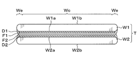
- the wafer processing system 1 As a polymerization substrate in which the first wafer W1 as the first substrate and the second wafer W2 as the second substrate are bonded. Processing is performed on the polymerized wafer T of. Then, in the wafer processing system 1, the peripheral portion We of the first wafer W1 is removed.
- the front surface W1a the surface on the side to be joined to the second wafer W2
- the back surface W1b the surface opposite to the front surface W1a
- the surface on the side to be joined to the first wafer W1 is referred to as the front surface W2a, and the surface opposite to the front surface W2a is referred to as the back surface W2b.
- a region radially inner of the peripheral edge portion We to be removed by edge trim is referred to as a central portion Wc.
- the first wafer W1 is a semiconductor wafer such as a silicon substrate, and a device layer D1 including a plurality of devices is formed on the surface W1a. Further, a surface film F1 which is a film for bonding with the second wafer W2 is further formed on the device layer D1 and is bonded to the second wafer W2 via the surface film F1. Examples of the surface film F1 include an oxide film (SiO 2 film, TEOS film), a SiC film, a SiCN film, an adhesive, and the like.
- the peripheral edge portion We of the first wafer W1 is chamfered, and the cross section of the peripheral edge portion We becomes thinner toward the tip thereof.
- the peripheral edge portion We is a portion that is removed in the edge trim described later, and is, for example, in the range of 0.5 mm to 3 mm in the radial direction from the outer end portion of the first wafer W1.
- a laser absorption layer (not shown) capable of absorbing the laser light irradiated to the inside of the polymerized wafer T when the peripheral edge portion We is removed is further formed. You may. Further, the surface film F1 formed on the device layer D1 may be used as the laser absorption layer.
- the second wafer W2 also has the same configuration as the first wafer W1, for example, a device layer D2 and a surface film F2 are formed on the surface W2a, and the peripheral edge portion is chamfered.
- the second wafer W2 does not have to be a device wafer on which the device layer D2 is formed, and may be, for example, a support wafer that supports the first wafer W1. In such a case, the second wafer W2 functions as a protective material for protecting the device layer D1 of the first wafer W1.
- the wafer processing system 1 has a configuration in which the loading / unloading block G1, the transport block G2, and the processing block G3 are integrally connected.
- the carry-in / out block G1, the transport block G2, and the processing block G3 are arranged side by side in this order from the negative direction side of the X-axis.
- a cassette C capable of accommodating a plurality of polymerized wafers T is carried in / out from the outside.
- the carry-in / out block G1 is provided with a cassette mounting stand 10.
- a plurality of, for example, three cassettes C can be freely mounted in a row on the cassette mounting table 10 in the Y-axis direction.
- the number of cassettes C mounted on the cassette mounting table 10 is not limited to this embodiment and can be arbitrarily determined.
- the transfer block G2 is provided with a wafer transfer device 20 adjacent to the cassette mounting table 10 on the X-axis positive direction side of the cassette mounting table 10.
- the wafer transfer device 20 is configured to be movable on a transfer path 21 extending in the Y-axis direction. Further, the wafer transfer device 20 has, for example, two transfer arms 22 and 22 that hold and transfer the polymerized wafer T.
- Each transport arm 22 is configured to be movable in the horizontal direction, the vertical direction, the horizontal axis, and the vertical axis.
- the configuration of the transport arm 22 is not limited to this embodiment, and any configuration can be adopted.
- the wafer transfer device 20 is configured to be able to transfer the polymerized wafer T to the cassette C of the cassette mounting table 10 and the transition device 30 described later.
- the transfer block G2 is provided with a transition device 30 for delivering the polymerized wafer T adjacent to the wafer transfer device 20 on the X-axis positive direction side of the wafer transfer device 20.
- the processing block G3 includes a wafer transfer device 40, a peripheral edge removing device 50, a cleaning device 60, a back surface inspection device 70, an internal reformer 80, and an interface reformer 90.
- the wafer transfer device 40 is configured to be movable on a transfer path 41 extending in the X-axis direction. Further, the wafer transfer device 40 has, for example, two transfer arms 42 and 42 that hold and transfer the polymerized wafer T. Each transport arm 42 is configured to be movable in the horizontal direction, the vertical direction, the horizontal axis, and the vertical axis. The configuration of the transport arm 42 is not limited to this embodiment, and any configuration can be adopted.
- the wafer transfer device 40 is configured to be able to transfer the polymerized wafer T to the transition device 30, the peripheral edge removing device 50, the cleaning device 60, the back surface inspection device 70, the internal reformer 80, and the interface reformer 90. There is.
- the peripheral edge removing device 50 removes the peripheral edge portion We of the first wafer W1, that is, edge trimming is performed.
- the cleaning device 60 cleans the polymerized wafer T.
- the back surface inspection device 70 is provided so as to be laminated with, for example, the cleaning device 60, and inspects the back surface of the polymerized wafer T after edge trimming.
- the internal reformer 80 irradiates the inside of the first wafer W1 with a laser beam (internal laser beam, for example, a YAG laser), and the peripheral surface reforming layer M1 serving as a base point for peeling the peripheral edge portion We and the peripheral edge portion We.
- a split reformed layer M2 is formed as a base point for fragmentation.
- Interface reformer 90 irradiates the first wafer W1 which is a base point of peeling of the periphery We on the interface of the second wafer W2 laser beam (surface laser beam, for example, CO 2 laser) and non below A junction region Ae is formed.
- first wafer W1 which is a base point of peeling of the periphery We on the interface of the second wafer W2 laser beam (surface laser beam, for example, CO 2 laser) and non below A junction region Ae is formed.
- the above wafer processing system 1 is provided with a control device 100 as a control unit.
- the control device 100 is, for example, a computer and has a program storage unit (not shown).
- the program storage unit stores a program that controls the processing of the polymerized wafer T in the wafer processing system 1. Further, the program storage unit also stores a program for controlling the operation of the drive system of the above-mentioned various processing devices and transfer devices to realize the wafer processing described later in the wafer processing system 1.
- the above program may be recorded on a storage medium H that can be read by a computer, and may be installed on the control device 100 from the storage medium H.
- the wafer processing system 1 is configured as described above. Next, the peripheral edge removing device 50 as the above-mentioned substrate processing device will be described.
- the peripheral edge removing device 50 has a chuck 51 as a holding member for holding the polymerized wafer T on the upper surface.
- the chuck 51 holds the back surface W2b of the second wafer W2 in a state where the first wafer W1 is arranged on the upper side and the second wafer W2 is arranged on the lower side.
- the chuck 51 is configured to be rotatable around a vertical axis by a rotation mechanism 52, and is configured to be able to adjust the relative circumferential position of the insertion member 53 described later with respect to the polymerization wafer T held on the chuck 51.
- An insertion member 53 as a removal member is provided on the side of the chuck 51 to remove the peripheral edge We of the first wafer W1 by being inserted into the interface between the first wafer W1 and the second wafer W2. ing.
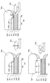
- the insertion member 53 has a shape with a pointed tip (for example, a wedge roller, a blade, etc.) in a side view, and is rotatably configured around a vertical axis by a rotation mechanism (not shown). Further, the insertion member 53 is configured to be movable in the advancing / retreating direction with respect to the polymerized wafer T held by the chuck 51 by the horizontal moving mechanism 54, and as shown in FIG. 4A, the chuck 51 is formed by the elevating mechanism 55. The height position relative to the polymerized wafer T held by the wafer T is adjustable.
- the insertion member 53 is moved in the horizontal direction by the horizontal movement mechanism 54, and the insertion member 53 is set between the surface W1a of the first wafer W1 and the surface W2a of the second wafer W2 as a target position.
- the peripheral edge portion We is pushed up from the second wafer W2, and then the chuck 51 is rotated with the insertion member 53 inserted into the interface, so that the peripheral edge portion We is the first wafer W1. It is peeled off from the (polymerized wafer T) and removed (hereinafter, the actual height position where the peripheral edge We peels off from the second wafer W2 may be referred to as a "peeling interface").
- a cup body 56 is provided so as to surround the chuck 51.
- a recovery mechanism (not shown) of the peripheral edge portion We is connected to the lower portion of the cup body 56 to receive the peripheral edge portion We of the first wafer W1 removed from the first wafer W1 by inserting the insertion member 53. Discharge to the collection mechanism.
- a height detection mechanism 57 for detecting the height position of the polymerized wafer T held by the chuck 51 and the insertion member 53 is provided above the chuck 51.
- the height detection mechanism 57 for example, a non-contact type laser displacement meter can be used. Then, the height detection mechanism 57 detects the height position of the polymerized wafer T held by the chuck 51 by, for example, irradiating the peripheral edge portion We with a laser beam from the back surface W1b side of the first wafer W1. The detected height position of the polymerized wafer T is output to the control device 100.
- the relative height position of the insertion member 53 with respect to the polymerization wafer T is determined based on the detected height position of the polymerization wafer T and the height position of the insertion member 53 acquired in advance. Adjust. In other words, the height position of the insertion member 53 is adjusted by the elevating mechanism 55 with reference to the detected height position of the laminated wafer T, and the height position of the insertion member 53 is set as the target position of the first wafer. Adjust between W1 and the second wafer W2.
- the height position of the insertion member 53 can be detected, for example, by moving the insertion member 53 below the height detection mechanism 57 by the horizontal movement mechanism 54. Further, for example, the height detection mechanism 57 may be moved by a moving mechanism (not shown) and may be detected by moving the height detecting mechanism 57 above the insertion member 53.
- the height detection mechanism 57 can detect whether or not the peripheral edge portion We is appropriately removed from the first wafer W1 by irradiating the polymerized wafer T after edge trim with a laser beam. Specifically, the height position is detected at the position corresponding to the peripheral edge portion We of the first wafer W1 after the edge trim, and the detected height position is the peripheral edge portion We of the first wafer W1 before the edge trimming. By comparing with the height position of, the presence or absence of the peripheral edge portion We after edge trimming can be detected. That is, the height detection mechanism 57 can operate as a "peeling inspection mechanism" according to the technique of the present disclosure.
- the presence or absence of the peripheral edge We after the edge trim is inspected by using a peeling inspection mechanism (not shown) for inspecting the presence or absence of the peripheral edge We after the edge trim instead of the height detection mechanism 57.
- the peeling inspection mechanism may inspect the presence or absence of the peripheral portion We by detecting the height position of the polymerized wafer T in the same manner as the height detection mechanism 57, and uses, for example, an imaging unit (for example, a CCD camera).
- the first wafer W1 after edge trimming may be imaged and inspected.
- the peripheral edge removing device 50 according to an example of the present embodiment is configured as described above, but the configuration of the peripheral edge removing device 50 is not limited to this.
- the relative circumferential position of the chuck 51 and the insertion member 53 is adjusted by rotating the chuck 51 by the rotation mechanism 52, but instead of or in addition to the rotation mechanism 52, the insertion member 53 may be configured to be movable along the circumferential direction of the laminated wafer T.
- the peripheral edge removing device 50 is further provided with a member inspection mechanism (not shown) for inspecting the state of the cutting edge of the insertion member 53, specifically, the presence or absence of a defect in the insertion member 53, the position of the defect, and the like. You may be.
- a member inspection mechanism for example, a CCD camera, a CMOS camera, or the like can be used.
- the insertion member 53 is moved up and down by the elevating mechanism 55 as shown in FIG. 4A to adjust the relative height position of the insertion member 53 with respect to the target position.
- the method of adjusting the height position of is not limited to this.
- the chuck 51 may be configured to be able to move up and down by an elevating mechanism, or for example, as shown in FIG. 4C, the horizontal movement mechanism 54 may be configured to be able to move up and down.
- the insertion member 53 may be configured to be able to move up and down integrally with the horizontal movement mechanism 54.
- the height position of the laminated wafer T is detected by irradiating the peripheral portion We with a laser beam from the back surface W1b side by the height detection mechanism 57, but the central portion of the first wafer W1.
- the height position of the laminated wafer T may be detected by irradiating the vicinity of the peripheral edge portion We in Wc with a laser beam.
- the height detection mechanism 57 may irradiate the laser beam from the back surface W2b side of the second wafer W2. That is, the height position of the insertion member 53 may be adjusted by the elevating mechanism 55 with reference to the back surface W2b of the second wafer W2.
- the height detection mechanism 57 is an imaging unit (for example, a CCD camera, a CMOS camera, etc.). ) May be used. That is, the polymerized wafer T held by the chuck 51 may be imaged, and the height position of the insertion member 53 may be adjusted based on the captured image.
- an imaging unit for example, a CCD camera, a CMOS camera, etc.
- the wafer processing performed by using the wafer processing system 1 configured as described above and the peripheral edge removing device 50 will be described.
- the first wafer W1 and the second wafer W2 are joined by a joining device (not shown) provided outside the wafer processing system 1, and a polymerized wafer T is formed in advance.
- the cassette C containing the plurality of polymerized wafers T is placed on the cassette mounting table 10 of the carry-in / out block G1, and then the polymerized wafer T in the cassette C is taken out by the wafer transfer device 20.
- the polymerized wafer T taken out from the cassette C is delivered to the wafer transfer device 40 via the transition device 30, and then transferred to the interface reformer 90.
- the interface modifier 90 as shown in FIG. 5A, the interface between the first wafer W1 and the device layer D1 (more specifically, the interface) while rotating the layered wafer T (first wafer W1). Is irradiated with a laser beam (for example, a CO 2 laser having a wavelength of 8.9 ⁇ m to 11 ⁇ m) to form the unbonded region Ae (step S1 in FIG. 6).
- a laser beam for example, a CO 2 laser having a wavelength of 8.9 ⁇ m to 11 ⁇ m
- the interface between the first wafer W1 and the device layer D1 is modified or peeled off, and the bonding strength between the first wafer W1 and the second wafer W2 is reduced or eliminated.
- the annular unbonded region Ae and the first wafer W1 and the second wafer W2 are bonded to the interface between the first wafer W1 and the device layer D1 in the radial direction of the unbonded region Ae.
- the junction region Ac is formed.
- the peripheral edge portion We of the first wafer W1 to be removed is removed, but the presence of the unbonded region Ae in this way makes it possible to appropriately remove the peripheral edge portion We. ..
- the polymerized wafer T on which the unbonded region Ae is formed is then transferred to the internal reformer 80 by the wafer transfer device 40.
- a peripheral reforming layer M1 and a split reforming layer M2 are formed inside the first wafer W1 (step S2 in FIG. 6).
- the peripheral edge modification layer M1 serves as a base point when removing the peripheral edge portion We in the edge trim described later.
- the split modified layer M2 serves as a base point for fragmentation of the peripheral portion We to be removed.
- the divisional modification layer M2 may be omitted in order to avoid complication of the illustration.
- the formation position of the peripheral modification layer M1 is determined to be slightly inward in the radial direction from the inner end of the unbonded region Ae formed in step S1.
- the peripheral modification layer M1 is formed at a position overlapping the boundary between the bonded region Ac and the unbonded region Ae (hereinafter, simply referred to as “boundary”), but is displaced in the radial direction due to, for example, a processing error. May be formed.
- the peripheral modification layer M1 is formed at a position radially outward from the boundary, that is, in the unbonded region Ae, the first wafer W1 floats with respect to the second wafer W2 after edge trimming. It may be in a state.
- the peripheral modification layer M1 by controlling the peripheral modification layer M1 to be formed radially inside the boundary, even if the formation position of the peripheral modification layer M1 is displaced, the position overlapping the boundary or the radial direction from the boundary Even on the outside, the peripheral modification layer M1 can be formed at a position close to the boundary, and the formation of the peripheral modification layer M1 at a position radially outward from the boundary can be suppressed.
- cracks C1 extend from the peripheral modification layer M1 in the thickness direction inside the first wafer W1.
- cracks C2 (not shown) extend from the split modified layer M2 in the thickness direction inside the first wafer W1.
- the polymerized wafer T in which the peripheral modification layer M1 and the split reforming layer M2 are formed inside the first wafer W1 is then transported to the peripheral edge removing device 50 by the wafer transfer device 40.
- the peripheral edge removing device 50 as shown in FIG. 5C, the peripheral edge portion We of the first wafer W1 is removed, that is, edge trimming is performed (step S3 in FIG. 6).
- the peripheral edge portion We is peeled off from the central portion Wc of the first wafer W1 with the peripheral edge modification layer M1 and the crack C1 as the base points, and the device layer D1 (second wafer W2) with the unbonded region Ae as the base point. Is peeled off from.
- the peripheral portion We to be removed is fragmented with the split reforming layer M2 and the crack C2 as the base points.
- the edge trim performed in the peripheral edge removing device 50 will be specifically described.
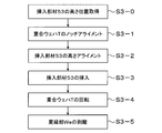
- the height position of the insertion member 53 inside the peripheral edge removing device 50 is acquired prior to carrying the polymerized wafer T into the peripheral edge removing device 50 (FIG. FIG. Step S3-0 of step 8).
- the horizontal movement mechanism 54 moves the insertion member 53 below the height detection mechanism 57, and the insertion member 53 is irradiated with laser light to detect the height position of the insertion member 53.
- the height position of the insertion member 53 may be detected and acquired by the height detection mechanism 57 for each processing of the polymerized wafer T in the peripheral edge removing device 50, or may be previously stored in the control device 100 for insertion. It may be acquired by referring to the height position of the member 53.
- the horizontal orientation (notch alignment) of the polymerized wafer T is adjusted (notch alignment) in the polymerized wafer T carried into the peripheral edge removing device 50 (step S3-1 in FIG. 8).
- the notch alignment the position of the notch portion (not shown) formed on the peripheral edge portion We of the first wafer W1 is detected while rotating the polymerized wafer T held by the chuck 51 by the rotation mechanism 52, and the notch alignment is performed. Adjust the position of the notch.
- the height position of the insertion member 53 inserted into the interface of the polymerized wafer T is adjusted (height alignment) (step S3-2 in FIG. 8).
- the height position of the upper surface of the polymerized wafer T held by the chuck 51 (the back surface W1b of the first wafer W1) is detected by using the height detection mechanism 57. do.
- the height position of the insertion member 53 is adjusted by the elevating mechanism 55 based on the detected height position of the upper surface of the polymerized wafer T and the height position of the insertion member 53 acquired in step S3-0.
- the height position of the insertion member 53 is determined at a predetermined position between the first wafer W1 and the second wafer W2, which is the target position for inserting the insertion member 53.
- the target position for inserting the insertion member 53 when removing the peripheral edge portion We when the polymerized wafer T is warped as described above, or when the in-plane thickness of the polymerized wafer or the device layer varies, the target position for inserting the insertion member 53 when removing the peripheral edge portion We.
- the polymerization wafer T is not stable in the circumferential direction.
- the target position is not stable in this way, when the laminated wafer T is rotated while inserting the insertion member 53 as described later, the target position deviates from the insertion height position of the insertion member 53. , There is a possibility that the peripheral portion We cannot be peeled off properly.
- the polymerization wafer T held by the chuck 51 is rotated by the rotation mechanism 52, and the peripheral portion We is irradiated with the laser beam to cover the entire circumference of the polymerization wafer T. Detect the height position. Then, as described later, when the polymerization wafer T is rotated to remove the peripheral portion We, the height position of the polymerization wafer T detected in this way and the relative circumferential direction of the insertion member 53 with respect to the polymerization wafer T. The height position of the insertion member 53 is adjusted based on the position.
- the insertion member 53 is then inserted into the target position using the horizontal movement mechanism 54 as shown in FIG. 9 (b) (step S3-3 in FIG. 8). Specifically, the insertion member 53 is inserted at the insertion height position determined in step S3-2, that is, at a predetermined position between the first wafer W1 and the second wafer W2.
- the insertion member 53 is inserted between the first wafer W1 and the second wafer W2, as shown in FIG. 9B, the peripheral edge We of the first wafer W1 becomes the second wafer W2.
- a stress N acts in the direction of peeling from the wafer, and then, as shown in FIG.
- the peripheral portion We peels off from the peripheral modified layer M1 and the crack C1 as base points.
- the insertion member 53 has, for example, a wedge shape, if the tip end portion of the insertion member 53 is inserted between the first wafer W1 and the second wafer W2, the peripheral edge of the insertion member 53 The stress N can be appropriately applied to the portion We.
- an unbonded region Ae is formed at the interface between the first wafer W1 and the device layer D1, whereby the bonding strength between the first wafer W1 and the second wafer W2 is reduced or eliminated. Therefore, when the stress N acts due to the insertion of the insertion member 53, the peripheral edge portion We is peeled off from the second wafer W2 with the unbonded region Ae in which the bonding strength is reduced as a base point.
- the peripheral edge We can be peeled off from the second wafer W2 with the unbonded region Ae as a base point.
- the peripheral edge portion We is appropriately removed even if the insertion height of the insertion member 53 with respect to the polymerized wafer T does not necessarily match the formation height of the unbonded region Ae which is the peeling interface. It can be removed from the second wafer W2.
- the insertion height of the insertion member 53 and the height position of the peeling interface of the peripheral edge portion We are different in this way, the insertion member 53 is suppressed from colliding with the polymerized wafer T, and the peripheral edge portion We is safely removed. be able to.
- the insertion height of the insertion member 53 with respect to the polymerized wafer T is more preferably the interface between the surface film F1 and the surface film F2, which is the bonding surface between the first wafer W1 and the second wafer W2.
- a space that is a non-bonding surface is slightly formed at the interface between the surface film F1 and the surface film F2, which is the bonding surface between the first wafer W1 and the second wafer W2. This is because the insertion member 53 is easily inserted into the space. Therefore, the stress N can be efficiently applied to the peeling interface.
- the insertion position of the insertion member 53 with respect to the circumferential direction of the polymerized wafer T is a region between one divided reformed layer M2 shown in FIG. 7 and another adjacent divided modified layer M2 (hereinafter, “divided region R”). ”), That is, it is preferable to avoid the formation position of the split-modifying layer M2.
- the insertion position of the insertion member 53 is on the upstream side of the division region R accompanying the rotation of the polymerization wafer T (near the above-mentioned one division modification layer M2). Is more preferable.
- the insertion member 53 When the insertion member 53 is inserted into the polymerization wafer T, the polymerization wafer T held by the chuck 51 is then rotated by the rotation mechanism 52, whereby the peripheral portion We is peeled off in the circumferential direction (rotation direction of the polymerization wafer T). It is extended (step S3-4 in FIG. 8). At this time, the insertion member 53 follows the rotation of the polymerized wafer T and rotates around the vertical axis. After that, when the insertion member 53 reaches the other end side of the division region R (near the other division modification layer M2 described above) as shown in FIG. 10B, the other division modification layer M2 is moved to the peripheral edge portion We.
- the peripheral edge portion We in the divided region R becomes the first. It is removed from the wafer W1 (polymerized wafer T) of No. 1 (step S3-5 in FIG. 8). The removed peripheral edge We falls into the cup body 56 due to its own weight, and is then collected by a collection mechanism (not shown).
- the insertion member 53 is retracted by the horizontal movement mechanism 54 before the peeling of the peripheral edge portion We is started, and the division region R avoiding the division modification layer M2. It is preferable that the insertion member 53 is inserted again on the upstream side of the above. Thereby, the peripheral portion We can be fragmented and removed more appropriately.
- the height position between the first wafer W1 and the second wafer W2, which is the target position is not stable in the circumferential direction of the polymerized wafer T, it accompanies the rotation of the polymerized wafer T.
- the insertion height position of the insertion member 53 and the target position may deviate from each other, and the peripheral edge portion We may not be properly removed.
- the height position of the insertion member 53 is adjusted according to the circumferential position of the polymerized wafer T based on the height position of the polymerized wafer T detected in step S3-2 on the entire circumference.
- the insertion height of the insertion member 53 on the entire circumference of the polymerized wafer T is calculated based on the detected height position on the entire circumference of the polymerized wafer T, and the insertion height is raised and lowered according to the calculated insertion height.
- the height of the insertion member 53 is adjusted by the mechanism 55. As a result, the peripheral portion We can be appropriately peeled off from the entire circumference of the polymerized wafer T.
- a process confirmation inspection for confirming the removal state of the peripheral portion We is subsequently performed (step S4 in FIG. 6).
- the height detection mechanism 57 is used to detect the height position at the position corresponding to the peripheral edge We after the edge trim, and the detected height position information is the height of the peripheral We before the edge trim. By comparing with the position information, it can be confirmed whether or not the peripheral portion We has been properly removed.
- the process confirmation inspection may be performed by using the image pickup unit as the height detection mechanism 57 as described above to image the position corresponding to the peripheral edge portion We after the edge trimming.
- the above-mentioned member inspection mechanism (not shown) may be used to inspect the insertion member 53 for the presence or absence of defects, the position of the defects, and the like. Further, the above-mentioned process confirmation inspection may be performed using the member inspection mechanism.
- the location where the edge trim is not properly performed that is, the circumferential position of the polymerized wafer T where the peripheral edge We remains, and the remaining peripheral edge The size of the part We is detected. Then, after the insertion member 53 is relatively moved to the peripheral position of the polymerization wafer T in which the peripheral edge portion We remain, the remaining peripheral edge portion We is removed by inserting the insertion member 53 again (step S3 in FIG. 6). Then, a process confirmation inspection (step S4 in FIG. 6) is performed after the removal process again.
- the insertion height of the insertion member 53 with respect to the polymerization wafer T is determined based on the height position detected during the process confirmation inspection in step S4. Alternatively, the determination may be made based on the height position detected during the height alignment in step S3-2.
- the polymerized wafer T determined to have been properly edge trimmed in the process confirmation inspection is then transferred to the cleaning device 60 by the wafer transfer device 40.
- the cleaning device 60 the polymerized wafer T after the peripheral edge portion We is removed is cleaned (step S5 in FIG. 6).
- the polymerized wafer T is transported to the back surface inspection device 70 by the wafer transfer device 40.
- the back surface inspection device 70 inspects the adhesion of particles to the back surface of the polymerized wafer T after the peripheral edge portion We is removed, that is, the back surface W2b of the second wafer W2 (step S6 in FIG. 6).
- the back surface inspection device 70 may further inspect the back surface W1b of the first wafer W1 together with the back surface W2b of the second wafer W2.
- the polymerized wafer T to which all the wafer processing has been performed is transferred to the cassette C of the cassette mounting table 10 by the wafer transfer device 20 via the transition device 30. In this way, a series of wafer processing in the wafer processing system 1 is completed.
- the insertion member 53 is configured to be able to move up and down by the elevating mechanism 55, so that the insertion height of the insertion member 53 is high.
- the position can be adjusted appropriately.
- the height position between the first wafer W1 and the second wafer W2, which is the target position for inserting the insertion member 53 is detected on the entire circumference of the polymerized wafer T, this target The insertion member 53 can be appropriately moved up and down according to the change in position. That is, according to the present embodiment, the peripheral edge portion We can be appropriately removed from the first wafer W1.
- the insertion member 53 is inserted, and the height position of the insertion member 53 when the polymerized wafer T is rotated. was adjusted to remove the peripheral We.
- the detection of the height position of the polymerized wafer T in the edge trim of the peripheral edge We (step S3 in FIG. 6) and the calculation of the insertion height of the insertion member 53 (hereinafter collectively referred to as "height position detection and the like").
- the timing of.) Is not limited to this.
- the height detection mechanism 57 detects the height position of the polymerized wafer T on the upstream side of the insertion position of the insertion member 53 in the rotation direction of the laminated wafer T, and based on the detected height position information, The insertion member 53 may be inserted and the height position may be adjusted on the downstream side of the height detection mechanism 57. In other words, the height position of the polymerized wafer T may be detected, the insertion member 53 may be inserted, and the height position may be adjusted at the same time.
- the height position of the insertion member 53 is adjusted based on the detected height position information.
- the height alignment and the removal of the peripheral portion We may be performed for each divided region. That is, for example, in the edge trim of step S3, the detection of the height position of the polymerized wafer T in one partition region and the removal of the peripheral edge We in the one partition region are repeated all around the polymerized wafer T. You may be cracked. Further, at this time, when the peripheral portion We is being removed in one divided region, the height position of the polymerized wafer T in the next divided region may be detected in parallel.
- the height position of the layered wafer T after detecting the height position of the layered wafer T, for example, on the downstream side of the height detection mechanism 57 in the rotation direction of the layered wafer T, or for example, detecting the height position.
- the detection of the height position and the adjustment of the height position may be performed at the same time. That is, the height position of the insertion member 53 may be made to follow in real time with respect to the height position information acquired by detecting the height position or the like.
- the method of adjusting the height position of the laminated wafer T is based on the height position detected by the laser displacement meter.
- the method is not limited, and the guide member may be brought into physical contact.
- the peripheral edge removing device 150 has a guide member 151 instead of the height detecting mechanism 57.
- the guide member 151 is an arm that integrally connects the contact member 152 (for example, a roller or the like) that travels in contact with the upper surface of the polymerized wafer T, that is, the back surface W1b of the first wafer W1, and the contact member 152 and the insertion member 53.
- a member 153 and a member 153 are provided.
- the relative height positional relationship between the contact member 152 and the insertion member 53 is set to be the distance from the back surface W1b of the first wafer W1 acquired in advance to the target position into which the insertion member 53 is inserted. ing.
- the insertion member 53 moves up and down integrally via the arm member 153 as the contact member 152 moves up and down. Further, the insertion member 53 is configured to be movable in the horizontal direction independently of the contact member 152 and the arm member 153 by the horizontal movement mechanism 54.
- the contact member 152 is brought into contact with the upper surface of the polymerization wafer T held by the chuck 51, that is, the back surface W1b of the first wafer W1.
- the contact member 152 moves up and down following a change in the height position of the upper surface of the polymerization wafer T.
- the insertion member 53 is integrally connected to the contact member 152 by the arm member 153, the insertion member 53 moves up and down following a change in the height position of the contact member 152, that is, a change in the height position of the upper surface of the polymerization wafer T. do.
- the relative height position of the contact member 152 and the insertion member 53 is set so that the height position of the insertion member 53 coincides with the target position, so that the insertion member 53 is at the target position. It goes up and down according to the change.
- the insertion member 53 by inserting the insertion member 53 into the layered wafer T with the contact member 152 in contact with the upper surface of the layered wafer T, the first wafer W1 and the second wafer W2, which are the target positions, can be brought into contact with each other. Even when the height position between them is not stable, the insertion height position of the insertion member 53 can be appropriately followed.
- the height position of the insertion member 53 is made to follow the target position calculated based on the height position of the polymerization wafer T, but the insertion inserted into the polymerization wafer T is performed.
- the height position of the member 53 may be fixed. That is, for example, when the target position calculated in the height alignment is stable over the entire circumference, or when the variation is within the allowable threshold even if it is not stable, the height position of the insertion member 53
- the peripheral edge We can be appropriately removed even when the peripheral portion We are fixed.
- the variation of the target position with respect to the threshold value can be calculated based on, for example, the average value, the median value, the maximum value, the minimum value, and the like of the detected height position information over the entire circumference.
- the insertion height position of the insertion member 53 with respect to the polymerization wafer T may be determined for each division region R of the peripheral edge portion We. Further, the variation of the target position with respect to the threshold value based on the average value, the median value, the maximum value, the minimum value, etc. of the height position information is calculated for each division region R of the peripheral portion We, and the height position of the insertion member 53 is fixed. Whether to make the insertion member 53 follow the target position may be determined for each division region R.
- the insertion height position of the insertion member 53 with respect to the polymerized wafer T follows the target position on the entire circumference of the peripheral edge We, but in such a case, control at the time of edge trim becomes complicated and the mechanism There is a concern that the burden on the victim will increase. Therefore, the insertion height position of the insertion member 53 is made to follow in the division region R where the variation of the target position with respect to the threshold value is large, and the insertion height position of the insertion member 53 is fixed in the division region R where the variation of the target position is small. ..
- the fixed height position of the insertion member 53 is set to the average value, the median value, and the median value of the height position information in a narrower range (close range). It can be calculated based on the maximum value, the minimum value, and the like. As a result, it is possible to suppress the variation between the insertion height position of the insertion member 53 and the target position as compared with the case of referring to the height position information on the entire circumference, and stable edge trim can be performed. Can be done.
- the insertion into the polymerization wafer T at the time of edge trimming is based on the height position of the polymerization wafer T detected by the height detection mechanism 57 and the height position of the insertion member 53 acquired in advance.
- the relative height position of the member 53 was adjusted by the elevating mechanism 55.
- the position adjustment of the insertion member 53 is not limited to the height direction, and the position is further adjusted in the horizontal direction (the insertion depth direction of the insertion member 53 with respect to the laminated wafer T) by the horizontal movement mechanism 54 at the time of edge trimming. May be done.
- the polymerized wafer T itself or the center of the peripherally modified layer M1 formed in an annular shape is held eccentrically with respect to the rotation center of the chuck 51 with respect to the chuck 51. May occur.
- the above-mentioned peripheral modification layer M1 may be formed eccentrically with respect to the first wafer W1 under various conditions. In such a case, even if the height position of the insertion member 53 with respect to the polymerization wafer T is appropriately controlled, the insertion member 53 is horizontal with respect to the formation position of the peripheral modification layer M1 when the chuck 51 (polymerization wafer T) is rotated during edge trimming. The direction position may change, and the peripheral portion We may not be properly removed. Therefore, in the present embodiment, the horizontal position of the insertion member 53 is controlled by the horizontal movement mechanism 54 following the eccentricity of the peripheral modification layer M1.
- the eccentricity detection mechanism 110 for detecting the amount is further provided.
- the eccentricity detection mechanism 110 can further detect the outer peripheral position of the polymerization wafer T or the horizontal position of the polymerization wafer T and the insertion member 53 in addition to the eccentricity of the peripheral modification layer M1 inside the first wafer W1. It may be configured. That is, the eccentricity detection mechanism 110 can operate as the "horizontal detection mechanism" according to the technique of the present disclosure.
- the eccentricity detection mechanism 110 for example, a non-contact laser displacement meter, a CCD camera, an IR camera, or the like can be used.
- the eccentricity detection mechanism 110 is, for example, the end position of the polymerized wafer T (first wafer W1, second wafer W2) and the formation position of the peripheral modification layer M1 (distance from the end position) on the entire circumference.
- the outer peripheral position of the polymerization wafer T (first wafer W1) or the eccentricity of the peripheral modification layer M1 formed inside the first wafer W1 is detected.
- the detected outer peripheral position or eccentricity amount is output to the control device 100.
- the peripheral edge removing device 50 inserts the peripheral edge portion We into the polymerized wafer T based on the detected outer peripheral position or the eccentricity amount of the peripheral edge modifying layer M1 and the horizontal position of the insertion member 53 capable of peeling the peripheral edge portion We acquired in advance.
- the relative horizontal position (insertion depth) of the member 53 is adjusted. Specifically, the detected outer peripheral position of the polymerized wafer T (first wafer W1), that is, the center of the polymerized wafer T (first wafer W1) held by the chuck 51 with respect to the rotation center of the chuck 51.
- the insertion depth of the insertion member 53 with respect to the target depth can be controlled by following the outer peripheral position of the polymerization wafer T (first wafer W1).
- the insertion depth of the insertion member 53 with respect to the target depth is controlled by following the eccentricity of the formation position. do.
- insertion depth refers to the distance between the outer end portion of the polymerization wafer T (first wafer W1) and the insertion member 53 when the insertion member 53 is inserted into the polymerization wafer T.
- target depth refers to the insertion depth of the insertion member 53 capable of peeling the peripheral edge portion We from the first wafer W.
- the insertion depth of the insertion member 53 may be fixed.
- the variation in the eccentricity with respect to the threshold is, for example, the outer peripheral portion of the polymerized wafer T (first wafer W1) detected by the eccentricity detection mechanism 110, or the formation position of the peripheral modification layer M1, that is, the end of the polymerized wafer T. It can be calculated based on the average value, the median value, the maximum value, the minimum value, and the like of the distance from the part position.
- the insertion depth of the insertion member 53 with respect to the polymerization wafer T may be determined for each division region R of the peripheral edge portion We. Further, the average value, the median value, the maximum value, the minimum value, etc. of the distance from the outer peripheral portion of the polymerization wafer T (first wafer W1) or the formation position of the peripheral modification layer M1, that is, the end position of the polymerization wafer T, etc.
- the variation in the amount of eccentricity with respect to the threshold value based on You may judge each time.
- the insertion height position of the insertion member 53 is determined for each division region R of the peripheral edge portion We, as in the case of determining the insertion height position. It is possible to easily control the edge trim and reduce the burden on the mechanism. Further, it is possible to suppress the occurrence of variation between the insertion depth of the insertion member 53 and the target depth, and it is possible to perform stable edge trim.
- the peripheral edge removing device may be further provided with a pressing member (not shown) for correcting the warp generated in the polymerized wafer T at least at the time of edge trimming of the first wafer W1.
- a pressing member (not shown) for correcting the warp generated in the polymerized wafer T at least at the time of edge trimming of the first wafer W1.
- the process is performed while continuously rotating the polymerized wafer T held by the chuck 51, but in such a case, it is inserted into the polymerized wafer T.
- the impact on the insertion member 53 is large, which may cause damage to the insertion member 53 or shorten the life of the insertion member 53.
- the impact on the insertion member 53 can be reduced by, for example, making the tip of the insertion member 53 an acute angle, but in such a case, the insertion member 53 may be damaged by a small impact, and the life of the insertion member 53 may also be shortened.
- the tip of the insertion member 53 is obtuse, the insertion member 53 is suppressed from being damaged, but the pressing load required to push up the peripheral portion We becomes large, which increases the risk of deterioration of edge trim quality and the polymerization wafer. The risk of damage to the T may increase.
- a predetermined position between the first wafer W1 and the second wafer W2, which is the target position, is determined in advance.
- a cut portion serving as a starting point of peeling may be formed at the formed position prior to the insertion of the insertion member 53.
- the peripheral edge removing device 250 is provided with a starting point forming member 251 for forming a notch Tc which is a starting point of peeling with respect to a target position.
- the configuration of the starting point forming member 251 is arbitrary, but for example, it has a rectangular plate-shaped blade portion 251a at the tip.
- the starting point forming member 251 is configured to be movable in the advancing / retreating direction with respect to the polymerization wafer T held by the chuck 51 by the horizontal movement mechanism 54, and the height position relative to the polymerization wafer T by the elevating mechanism 55. Is configured to be adjustable.
- the starting point forming member 251 may be configured to be movable integrally with the insertion member 53, or may be configured to be movable independently of the insertion member 53.
- the blade portion 251a of the starting point forming member 251 is inserted with respect to the target position to form the cut portion Tc.
- the number of cut portions Tc formed in the circumferential direction of the polymerized wafer T can be arbitrarily determined, and may be formed at only one location in the circumferential direction, or may be formed at a plurality of locations. Further, for example, the cut portion Tc may be formed on the entire circumference of the polymerization wafer T.
- the insertion member 53 is inserted into the notch Tc formed at the target position in this way.
- the peripheral portion We is peeled off starting from the cut portion Tc formed at the target position, the peripheral portion We can be easily peeled off.
- the pressing load applied to the insertion of the insertion member 53 can be reduced, and the risk of deterioration of the edge trim quality and the risk of damage to the polymerized wafer T are reduced. be able to. Further, it is possible to reduce the risk of the insertion member 53 being damaged or the life being shortened.
- the formed notch Tc may be expanded in the thickness direction of the polymerized wafer T.
- the cut portion Tc formed can be expanded by swinging the starting point forming member 251 in the vertical direction by the elevating mechanism 55 when the blade portion 251a is inserted with respect to the target position.
- the height detection mechanism 57 is configured so that the height alignment of the starting point forming member 251 can be further performed.
- the starting point forming member 251 be movable below the height detecting mechanism 57 by, for example, the horizontal moving mechanism 54 and the elevating mechanism 55.
- the height detection mechanism 57 may be configured to be movable above the starting point forming member 251.
- a member inspection mechanism (not shown) is used to check for the presence or absence of the starting point forming member 251. It may be configured so that the position of the above can be further inspected.
- the case where the peripheral portion We of the first wafer W1 is removed in the polymerized wafer T in which the first wafer W1 and the second wafer W2 are joined has been described as an example.
- the technique according to the present disclosure can be applied even when the first wafer W1 is separated into a front surface W1a side and a back surface W1b side and thinned.
- the peripheral modification layer M1 which is the starting point of peeling of the peripheral edge portion We of the first wafer W1 and the internal surface modification which is the starting point of separation are inside the first wafer W1.
- the peripheral edge We of the first wafer W1 is removed from the second wafer W2 (polymerized wafer T) integrally with the back surface W1b side of the first wafer W1.
- the height position of the insertion member 53 with respect to the height position between the first wafer W1 and the second wafer W2, which is the target position for inserting the insertion member 53 can be appropriately adjusted.
- the entire first wafer W1 is removed from the second wafer W2, and the device layer D1 formed on the first wafer W1 is transferred to the second wafer W2. That is, it can also be applied to the laser lift-off process of the polymerized wafer T.
- the first wafer is based on the unbonded region Ae. Insertion into the height position between the first wafer W1 and the second wafer W2, which is the target position for inserting the insertion member 53 when the entire surface of W1 is peeled from the second wafer W2 (polymerized wafer T). The height position of the member 53 can be adjusted appropriately.
- the unbonded region Ae is formed in the interface reformer 90 of the wafer processing system 1, but the formation timing of the unbonded region Ae is not limited to this.
- the unbonded region Ae may be formed on the polymerized wafer T after the polymerized wafer T is formed and before being carried into the wafer processing system 1.
- an unbonded region Ae may be formed on the first wafer W1 before joining the second wafer W2 outside the wafer processing system 1.
- the formation position of the unbonded region Ae is not limited to the interface between the first wafer W1 and the device layer D1, and may be formed on, for example, the surface film F1, or the first wafer W1 and the second wafer W2. It may be formed at the bonding interface of.
Landscapes
- Engineering & Computer Science (AREA)
- Physics & Mathematics (AREA)
- Optics & Photonics (AREA)
- Chemical & Material Sciences (AREA)
- Chemical Kinetics & Catalysis (AREA)
- General Chemical & Material Sciences (AREA)
- Oil, Petroleum & Natural Gas (AREA)
- Plasma & Fusion (AREA)
- Mechanical Engineering (AREA)
- Container, Conveyance, Adherence, Positioning, Of Wafer (AREA)
- Mechanical Treatment Of Semiconductor (AREA)
Priority Applications (7)
| Application Number | Priority Date | Filing Date | Title |
|---|---|---|---|
| US17/996,507 US12543525B2 (en) | 2020-04-20 | 2021-03-16 | Substrate processing apparatus and substrate processing method |
| KR1020257025640A KR20250119666A (ko) | 2020-04-20 | 2021-03-16 | 기판 처리 장치 및 기판 처리 방법 |
| KR1020227040132A KR102842163B1 (ko) | 2020-04-20 | 2021-03-16 | 기판 처리 장치 및 기판 처리 방법 |
| CN202180028326.3A CN115398599A (zh) | 2020-04-20 | 2021-03-16 | 基板处理装置和基板处理方法 |
| JP2022516887A JP7398554B2 (ja) | 2020-04-20 | 2021-03-16 | 基板処理装置及び基板処理方法 |
| JP2023204420A JP7611350B2 (ja) | 2020-04-20 | 2023-12-04 | 基板処理装置及び基板処理方法 |
| US19/430,364 US20260123330A1 (en) | 2020-04-20 | 2025-12-23 | Substrate processing apparatus and substrate processing method |
Applications Claiming Priority (2)
| Application Number | Priority Date | Filing Date | Title |
|---|---|---|---|
| JP2020-074921 | 2020-04-20 | ||
| JP2020074921 | 2020-04-20 |
Related Child Applications (2)
| Application Number | Title | Priority Date | Filing Date |
|---|---|---|---|
| US17/996,507 A-371-Of-International US12543525B2 (en) | 2020-04-20 | 2021-03-16 | Substrate processing apparatus and substrate processing method |
| US19/430,364 Continuation US20260123330A1 (en) | 2020-04-20 | 2025-12-23 | Substrate processing apparatus and substrate processing method |
Publications (1)
| Publication Number | Publication Date |
|---|---|
| WO2021215145A1 true WO2021215145A1 (ja) | 2021-10-28 |
Family
ID=78270699
Family Applications (1)
| Application Number | Title | Priority Date | Filing Date |
|---|---|---|---|
| PCT/JP2021/010662 Ceased WO2021215145A1 (ja) | 2020-04-20 | 2021-03-16 | 基板処理装置及び基板処理方法 |
Country Status (5)
| Country | Link |
|---|---|
| US (2) | US12543525B2 (https=) |
| JP (2) | JP7398554B2 (https=) |
| KR (2) | KR20250119666A (https=) |
| CN (1) | CN115398599A (https=) |
| WO (1) | WO2021215145A1 (https=) |
Cited By (2)
| Publication number | Priority date | Publication date | Assignee | Title |
|---|---|---|---|---|
| WO2024241699A1 (ja) * | 2023-05-23 | 2024-11-28 | 東京エレクトロン株式会社 | 基板処理方法及び基板処理システム |
| WO2025079432A1 (ja) * | 2023-10-10 | 2025-04-17 | 東京エレクトロン株式会社 | 処理方法、処理システム及び検査装置 |
Families Citing this family (2)
| Publication number | Priority date | Publication date | Assignee | Title |
|---|---|---|---|---|
| TWI855139B (zh) * | 2019-10-28 | 2024-09-11 | 日商東京威力科創股份有限公司 | 基板處理方法及基板處理系統 |
| JP2024030643A (ja) * | 2022-08-24 | 2024-03-07 | キオクシア株式会社 | 半導体製造装置および半導体装置の製造方法 |
Citations (6)
| Publication number | Priority date | Publication date | Assignee | Title |
|---|---|---|---|---|
| JP2008537316A (ja) * | 2005-04-19 | 2008-09-11 | 株式会社荏原製作所 | 基板処理装置 |
| US20160093518A1 (en) * | 2014-09-29 | 2016-03-31 | Samsung Electronics Co., Ltd. | Initiator and method for debonding wafer supporting system |
| WO2019176589A1 (ja) * | 2018-03-14 | 2019-09-19 | 東京エレクトロン株式会社 | 基板処理システム、基板処理方法及びコンピュータ記憶媒体 |
| WO2019208359A1 (ja) * | 2018-04-27 | 2019-10-31 | 東京エレクトロン株式会社 | 基板処理システム及び基板処理方法 |
| WO2019208298A1 (ja) * | 2018-04-27 | 2019-10-31 | 東京エレクトロン株式会社 | 基板処理システム及び基板処理方法 |
| JP3225828U (ja) * | 2020-01-28 | 2020-04-09 | 東京エレクトロン株式会社 | 回収ボックス |
Family Cites Families (7)
| Publication number | Priority date | Publication date | Assignee | Title |
|---|---|---|---|---|
| JP2006093333A (ja) * | 2004-09-22 | 2006-04-06 | Disco Abrasive Syst Ltd | 切削方法 |
| JP5988765B2 (ja) | 2012-08-13 | 2016-09-07 | ダイトエレクトロン株式会社 | ウェーハの面取り加工方法、ウェーハの面取り加工装置および砥石角度調整用治具 |
| JP5909453B2 (ja) * | 2013-03-07 | 2016-04-26 | 東京エレクトロン株式会社 | 剥離装置、剥離システムおよび剥離方法 |
| JP6182476B2 (ja) * | 2014-02-17 | 2017-08-16 | 東京エレクトロン株式会社 | 気泡除去装置、気泡除去方法および接合システム |
| JP6475071B2 (ja) | 2015-04-24 | 2019-02-27 | 株式会社Screenホールディングス | 基板処理装置および基板処理方法 |
| JP6537992B2 (ja) * | 2016-03-30 | 2019-07-03 | 東京エレクトロン株式会社 | 基板処理装置、基板処理装置の制御方法、及び基板処理システム |
| JP6882033B2 (ja) | 2017-03-29 | 2021-06-02 | 株式会社東京精密 | ウェーハの位置決め装置及びそれを用いた面取り装置 |
-
2021
- 2021-03-16 CN CN202180028326.3A patent/CN115398599A/zh active Pending
- 2021-03-16 WO PCT/JP2021/010662 patent/WO2021215145A1/ja not_active Ceased
- 2021-03-16 US US17/996,507 patent/US12543525B2/en active Active
- 2021-03-16 JP JP2022516887A patent/JP7398554B2/ja active Active
- 2021-03-16 KR KR1020257025640A patent/KR20250119666A/ko active Pending
- 2021-03-16 KR KR1020227040132A patent/KR102842163B1/ko active Active
-
2023
- 2023-12-04 JP JP2023204420A patent/JP7611350B2/ja active Active
-
2025
- 2025-12-23 US US19/430,364 patent/US20260123330A1/en active Pending
Patent Citations (6)
| Publication number | Priority date | Publication date | Assignee | Title |
|---|---|---|---|---|
| JP2008537316A (ja) * | 2005-04-19 | 2008-09-11 | 株式会社荏原製作所 | 基板処理装置 |
| US20160093518A1 (en) * | 2014-09-29 | 2016-03-31 | Samsung Electronics Co., Ltd. | Initiator and method for debonding wafer supporting system |
| WO2019176589A1 (ja) * | 2018-03-14 | 2019-09-19 | 東京エレクトロン株式会社 | 基板処理システム、基板処理方法及びコンピュータ記憶媒体 |
| WO2019208359A1 (ja) * | 2018-04-27 | 2019-10-31 | 東京エレクトロン株式会社 | 基板処理システム及び基板処理方法 |
| WO2019208298A1 (ja) * | 2018-04-27 | 2019-10-31 | 東京エレクトロン株式会社 | 基板処理システム及び基板処理方法 |
| JP3225828U (ja) * | 2020-01-28 | 2020-04-09 | 東京エレクトロン株式会社 | 回収ボックス |
Cited By (2)
| Publication number | Priority date | Publication date | Assignee | Title |
|---|---|---|---|---|
| WO2024241699A1 (ja) * | 2023-05-23 | 2024-11-28 | 東京エレクトロン株式会社 | 基板処理方法及び基板処理システム |
| WO2025079432A1 (ja) * | 2023-10-10 | 2025-04-17 | 東京エレクトロン株式会社 | 処理方法、処理システム及び検査装置 |
Also Published As
| Publication number | Publication date |
|---|---|
| JP7398554B2 (ja) | 2023-12-14 |
| CN115398599A (zh) | 2022-11-25 |
| US20260123330A1 (en) | 2026-04-30 |
| US20230207344A1 (en) | 2023-06-29 |
| US12543525B2 (en) | 2026-02-03 |
| KR102842163B1 (ko) | 2025-08-04 |
| KR20230004673A (ko) | 2023-01-06 |
| KR20250119666A (ko) | 2025-08-07 |
| JPWO2021215145A1 (https=) | 2021-10-28 |
| JP7611350B2 (ja) | 2025-01-09 |
| JP2024019282A (ja) | 2024-02-08 |
Similar Documents
| Publication | Publication Date | Title |
|---|---|---|
| JP7611350B2 (ja) | 基板処理装置及び基板処理方法 | |
| KR102735652B1 (ko) | 기판 처리 장치 및 기판 처리 방법 | |
| JP7413468B2 (ja) | 基板処理装置及び基板処理方法 | |
| JP2021174806A (ja) | 基板処理装置及び基板処理方法 | |
| JP7780534B2 (ja) | 処理方法及び処理システム | |
| JP7688216B2 (ja) | 基板処理方法及び基板処理装置 | |
| JP7784443B2 (ja) | 処理方法及び処理システム | |
| CN114599479A (zh) | 基板处理方法和基板处理系统 | |
| JP7221076B2 (ja) | レーザー加工装置の設定方法、レーザー加工方法、レーザー加工装置、薄化システム、および基板処理方法 | |
| WO2021172085A1 (ja) | 基板処理方法及び基板処理装置 | |
| JP2021068867A (ja) | 基板処理方法及び基板処理システム | |
| JP7398242B2 (ja) | 基板処理方法及び基板処理システム | |
| JP7550018B2 (ja) | 処理方法及び処理システム | |
| JP2021068869A (ja) | 基板処理方法及び基板処理システム | |
| JP7499599B2 (ja) | 基板処理システム及び基板処理方法 | |
| JP2026063154A (ja) | 基板処理システム及び基板処理方法 | |
| JP2025013658A (ja) | 基板処理装置 | |
| JP2023003476A (ja) | 処理方法及び処理システム | |
| JP2024087506A (ja) | 基板処理方法及びウェハ処理システム | |
| WO2024241699A1 (ja) | 基板処理方法及び基板処理システム | |
| WO2024247740A1 (ja) | 基板処理方法及び基板処理システム |
Legal Events
| Date | Code | Title | Description |
|---|---|---|---|
| 121 | Ep: the epo has been informed by wipo that ep was designated in this application |
Ref document number: 21792168 Country of ref document: EP Kind code of ref document: A1 |
|
| ENP | Entry into the national phase |
Ref document number: 2022516887 Country of ref document: JP Kind code of ref document: A |
|
| ENP | Entry into the national phase |
Ref document number: 20227040132 Country of ref document: KR Kind code of ref document: A |
|
| NENP | Non-entry into the national phase |
Ref country code: DE |
|
| 122 | Ep: pct application non-entry in european phase |
Ref document number: 21792168 Country of ref document: EP Kind code of ref document: A1 |
|
| WWD | Wipo information: divisional of initial pct application |
Ref document number: 1020257025640 Country of ref document: KR |
|
| WWP | Wipo information: published in national office |
Ref document number: 1020257025640 Country of ref document: KR |
|
| WWG | Wipo information: grant in national office |
Ref document number: 17996507 Country of ref document: US |