WO2021210600A1 - 電力用半導体装置、電力用半導体装置の製造方法および電力変換装置 - Google Patents
電力用半導体装置、電力用半導体装置の製造方法および電力変換装置 Download PDFInfo
- Publication number
- WO2021210600A1 WO2021210600A1 PCT/JP2021/015421 JP2021015421W WO2021210600A1 WO 2021210600 A1 WO2021210600 A1 WO 2021210600A1 JP 2021015421 W JP2021015421 W JP 2021015421W WO 2021210600 A1 WO2021210600 A1 WO 2021210600A1
- Authority
- WO
- WIPO (PCT)
- Prior art keywords
- impurity region
- semiconductor device
- gate electrode
- sic
- region
- Prior art date
- Legal status (The legal status is an assumption and is not a legal conclusion. Google has not performed a legal analysis and makes no representation as to the accuracy of the status listed.)
- Ceased
Links
Images


Classifications
-
- H—ELECTRICITY
- H10—SEMICONDUCTOR DEVICES; ELECTRIC SOLID-STATE DEVICES NOT OTHERWISE PROVIDED FOR
- H10D—INORGANIC ELECTRIC SEMICONDUCTOR DEVICES
- H10D30/00—Field-effect transistors [FET]
- H10D30/60—Insulated-gate field-effect transistors [IGFET]
- H10D30/64—Double-diffused metal-oxide semiconductor [DMOS] FETs
- H10D30/66—Vertical DMOS [VDMOS] FETs
- H10D30/668—Vertical DMOS [VDMOS] FETs having trench gate electrodes, e.g. UMOS transistors
-
- H—ELECTRICITY
- H02—GENERATION; CONVERSION OR DISTRIBUTION OF ELECTRIC POWER
- H02M—APPARATUS FOR CONVERSION BETWEEN AC AND AC, BETWEEN AC AND DC, OR BETWEEN DC AND DC, AND FOR USE WITH MAINS OR SIMILAR POWER SUPPLY SYSTEMS; CONVERSION OF DC OR AC INPUT POWER INTO SURGE OUTPUT POWER; CONTROL OR REGULATION THEREOF
- H02M1/00—Details of apparatus for conversion
- H02M1/08—Circuits specially adapted for the generation of control voltages for semiconductor devices incorporated in static converters
-
- H—ELECTRICITY
- H10—SEMICONDUCTOR DEVICES; ELECTRIC SOLID-STATE DEVICES NOT OTHERWISE PROVIDED FOR
- H10D—INORGANIC ELECTRIC SEMICONDUCTOR DEVICES
- H10D12/00—Bipolar devices controlled by the field effect, e.g. insulated-gate bipolar transistors [IGBT]
- H10D12/01—Manufacture or treatment
- H10D12/031—Manufacture or treatment of IGBTs
-
- H—ELECTRICITY
- H10—SEMICONDUCTOR DEVICES; ELECTRIC SOLID-STATE DEVICES NOT OTHERWISE PROVIDED FOR
- H10D—INORGANIC ELECTRIC SEMICONDUCTOR DEVICES
- H10D30/00—Field-effect transistors [FET]
- H10D30/01—Manufacture or treatment
- H10D30/021—Manufacture or treatment of FETs having insulated gates [IGFET]
- H10D30/028—Manufacture or treatment of FETs having insulated gates [IGFET] of double-diffused metal oxide semiconductor [DMOS] FETs
- H10D30/0291—Manufacture or treatment of FETs having insulated gates [IGFET] of double-diffused metal oxide semiconductor [DMOS] FETs of vertical DMOS [VDMOS] FETs
- H10D30/0297—Manufacture or treatment of FETs having insulated gates [IGFET] of double-diffused metal oxide semiconductor [DMOS] FETs of vertical DMOS [VDMOS] FETs using recessing of the gate electrodes, e.g. to form trench gate electrodes
-
- H—ELECTRICITY
- H10—SEMICONDUCTOR DEVICES; ELECTRIC SOLID-STATE DEVICES NOT OTHERWISE PROVIDED FOR
- H10D—INORGANIC ELECTRIC SEMICONDUCTOR DEVICES
- H10D30/00—Field-effect transistors [FET]
- H10D30/60—Insulated-gate field-effect transistors [IGFET]
-
- H—ELECTRICITY
- H10—SEMICONDUCTOR DEVICES; ELECTRIC SOLID-STATE DEVICES NOT OTHERWISE PROVIDED FOR
- H10D—INORGANIC ELECTRIC SEMICONDUCTOR DEVICES
- H10D62/00—Semiconductor bodies, or regions thereof, of devices having potential barriers
- H10D62/10—Shapes, relative sizes or dispositions of the regions of the semiconductor bodies; Shapes of the semiconductor bodies
- H10D62/102—Constructional design considerations for preventing surface leakage or controlling electric field concentration
- H10D62/103—Constructional design considerations for preventing surface leakage or controlling electric field concentration for increasing or controlling the breakdown voltage of reverse-biased devices
- H10D62/105—Constructional design considerations for preventing surface leakage or controlling electric field concentration for increasing or controlling the breakdown voltage of reverse-biased devices by having particular doping profiles, shapes or arrangements of PN junctions; by having supplementary regions, e.g. junction termination extension [JTE]
- H10D62/109—Reduced surface field [RESURF] PN junction structures
-
- H—ELECTRICITY
- H10—SEMICONDUCTOR DEVICES; ELECTRIC SOLID-STATE DEVICES NOT OTHERWISE PROVIDED FOR
- H10D—INORGANIC ELECTRIC SEMICONDUCTOR DEVICES
- H10D62/00—Semiconductor bodies, or regions thereof, of devices having potential barriers
- H10D62/10—Shapes, relative sizes or dispositions of the regions of the semiconductor bodies; Shapes of the semiconductor bodies
- H10D62/113—Isolations within a component, i.e. internal isolations
- H10D62/115—Dielectric isolations, e.g. air gaps
- H10D62/116—Dielectric isolations, e.g. air gaps adjoining the input or output regions of field-effect devices, e.g. adjoining source or drain regions
-
- H—ELECTRICITY
- H10—SEMICONDUCTOR DEVICES; ELECTRIC SOLID-STATE DEVICES NOT OTHERWISE PROVIDED FOR
- H10D—INORGANIC ELECTRIC SEMICONDUCTOR DEVICES
- H10D62/00—Semiconductor bodies, or regions thereof, of devices having potential barriers
- H10D62/10—Shapes, relative sizes or dispositions of the regions of the semiconductor bodies; Shapes of the semiconductor bodies
- H10D62/17—Semiconductor regions connected to electrodes not carrying current to be rectified, amplified or switched, e.g. channel regions
- H10D62/393—Body regions of DMOS transistors or IGBTs
-
- H—ELECTRICITY
- H10—SEMICONDUCTOR DEVICES; ELECTRIC SOLID-STATE DEVICES NOT OTHERWISE PROVIDED FOR
- H10D—INORGANIC ELECTRIC SEMICONDUCTOR DEVICES
- H10D62/00—Semiconductor bodies, or regions thereof, of devices having potential barriers
- H10D62/80—Semiconductor bodies, or regions thereof, of devices having potential barriers characterised by the materials
- H10D62/83—Semiconductor bodies, or regions thereof, of devices having potential barriers characterised by the materials being Group IV materials, e.g. B-doped Si or undoped Ge
- H10D62/832—Semiconductor bodies, or regions thereof, of devices having potential barriers characterised by the materials being Group IV materials, e.g. B-doped Si or undoped Ge being Group IV materials comprising two or more elements, e.g. SiGe
- H10D62/8325—Silicon carbide
-
- H—ELECTRICITY
- H10—SEMICONDUCTOR DEVICES; ELECTRIC SOLID-STATE DEVICES NOT OTHERWISE PROVIDED FOR
- H10D—INORGANIC ELECTRIC SEMICONDUCTOR DEVICES
- H10D64/00—Electrodes of devices having potential barriers
- H10D64/01—Manufacture or treatment
- H10D64/011—Manufacture or treatment of electrodes ohmically coupled to a semiconductor
-
- H—ELECTRICITY
- H10—SEMICONDUCTOR DEVICES; ELECTRIC SOLID-STATE DEVICES NOT OTHERWISE PROVIDED FOR
- H10D—INORGANIC ELECTRIC SEMICONDUCTOR DEVICES
- H10D64/00—Electrodes of devices having potential barriers
- H10D64/20—Electrodes characterised by their shapes, relative sizes or dispositions
- H10D64/27—Electrodes not carrying the current to be rectified, amplified, oscillated or switched, e.g. gates
- H10D64/311—Gate electrodes for field-effect devices
- H10D64/411—Gate electrodes for field-effect devices for FETs
- H10D64/511—Gate electrodes for field-effect devices for FETs for IGFETs
- H10D64/517—Gate electrodes for field-effect devices for FETs for IGFETs characterised by the conducting layers
- H10D64/518—Gate electrodes for field-effect devices for FETs for IGFETs characterised by the conducting layers characterised by their lengths or sectional shapes
-
- H—ELECTRICITY
- H10—SEMICONDUCTOR DEVICES; ELECTRIC SOLID-STATE DEVICES NOT OTHERWISE PROVIDED FOR
- H10W—GENERIC PACKAGES, INTERCONNECTIONS, CONNECTORS OR OTHER CONSTRUCTIONAL DETAILS OF DEVICES COVERED BY CLASS H10
- H10W90/00—Package configurations
-
- H—ELECTRICITY
- H02—GENERATION; CONVERSION OR DISTRIBUTION OF ELECTRIC POWER
- H02M—APPARATUS FOR CONVERSION BETWEEN AC AND AC, BETWEEN AC AND DC, OR BETWEEN DC AND DC, AND FOR USE WITH MAINS OR SIMILAR POWER SUPPLY SYSTEMS; CONVERSION OF DC OR AC INPUT POWER INTO SURGE OUTPUT POWER; CONTROL OR REGULATION THEREOF
- H02M7/00—Conversion of AC power input into DC power output; Conversion of DC power input into AC power output
- H02M7/42—Conversion of DC power input into AC power output without possibility of reversal
- H02M7/44—Conversion of DC power input into AC power output without possibility of reversal by static converters
- H02M7/48—Conversion of DC power input into AC power output without possibility of reversal by static converters using discharge tubes with control electrode or semiconductor devices with control electrode
- H02M7/53—Conversion of DC power input into AC power output without possibility of reversal by static converters using discharge tubes with control electrode or semiconductor devices with control electrode using devices of a triode or transistor type requiring continuous application of a control signal
- H02M7/537—Conversion of DC power input into AC power output without possibility of reversal by static converters using discharge tubes with control electrode or semiconductor devices with control electrode using devices of a triode or transistor type requiring continuous application of a control signal using semiconductor devices only, e.g. single switched pulse inverters
- H02M7/5387—Conversion of DC power input into AC power output without possibility of reversal by static converters using discharge tubes with control electrode or semiconductor devices with control electrode using devices of a triode or transistor type requiring continuous application of a control signal using semiconductor devices only, e.g. single switched pulse inverters in a bridge configuration
- H02M7/53871—Conversion of DC power input into AC power output without possibility of reversal by static converters using discharge tubes with control electrode or semiconductor devices with control electrode using devices of a triode or transistor type requiring continuous application of a control signal using semiconductor devices only, e.g. single switched pulse inverters in a bridge configuration with automatic control of output voltage or current
-
- H—ELECTRICITY
- H02—GENERATION; CONVERSION OR DISTRIBUTION OF ELECTRIC POWER
- H02P—CONTROL OR REGULATION OF ELECTRIC MOTORS, ELECTRIC GENERATORS OR DYNAMO-ELECTRIC CONVERTERS; CONTROLLING TRANSFORMERS, REACTORS OR CHOKE COILS
- H02P27/00—Arrangements or methods for the control of AC motors characterised by the kind of supply voltage
- H02P27/04—Arrangements or methods for the control of AC motors characterised by the kind of supply voltage using variable-frequency supply voltage, e.g. inverter or converter supply voltage
- H02P27/06—Arrangements or methods for the control of AC motors characterised by the kind of supply voltage using variable-frequency supply voltage, e.g. inverter or converter supply voltage using DC to AC converters or inverters
- H02P27/08—Arrangements or methods for the control of AC motors characterised by the kind of supply voltage using variable-frequency supply voltage, e.g. inverter or converter supply voltage using DC to AC converters or inverters with pulse width modulation
-
- H—ELECTRICITY
- H10—SEMICONDUCTOR DEVICES; ELECTRIC SOLID-STATE DEVICES NOT OTHERWISE PROVIDED FOR
- H10W—GENERIC PACKAGES, INTERCONNECTIONS, CONNECTORS OR OTHER CONSTRUCTIONAL DETAILS OF DEVICES COVERED BY CLASS H10
- H10W72/00—Interconnections or connectors in packages
- H10W72/071—Connecting or disconnecting
- H10W72/073—Connecting or disconnecting of die-attach connectors
- H10W72/07351—Connecting or disconnecting of die-attach connectors characterised by changes in properties of the die-attach connectors during connecting
- H10W72/07354—Connecting or disconnecting of die-attach connectors characterised by changes in properties of the die-attach connectors during connecting changes in dispositions
-
- H—ELECTRICITY
- H10—SEMICONDUCTOR DEVICES; ELECTRIC SOLID-STATE DEVICES NOT OTHERWISE PROVIDED FOR
- H10W—GENERIC PACKAGES, INTERCONNECTIONS, CONNECTORS OR OTHER CONSTRUCTIONAL DETAILS OF DEVICES COVERED BY CLASS H10
- H10W72/00—Interconnections or connectors in packages
- H10W72/30—Die-attach connectors
- H10W72/341—Dispositions of die-attach connectors, e.g. layouts
- H10W72/347—Dispositions of multiple die-attach connectors
-
- H—ELECTRICITY
- H10—SEMICONDUCTOR DEVICES; ELECTRIC SOLID-STATE DEVICES NOT OTHERWISE PROVIDED FOR
- H10W—GENERIC PACKAGES, INTERCONNECTIONS, CONNECTORS OR OTHER CONSTRUCTIONAL DETAILS OF DEVICES COVERED BY CLASS H10
- H10W72/00—Interconnections or connectors in packages
- H10W72/50—Bond wires
- H10W72/531—Shapes of wire connectors
- H10W72/5363—Shapes of wire connectors the connected ends being wedge-shaped
-
- H—ELECTRICITY
- H10—SEMICONDUCTOR DEVICES; ELECTRIC SOLID-STATE DEVICES NOT OTHERWISE PROVIDED FOR
- H10W—GENERIC PACKAGES, INTERCONNECTIONS, CONNECTORS OR OTHER CONSTRUCTIONAL DETAILS OF DEVICES COVERED BY CLASS H10
- H10W72/00—Interconnections or connectors in packages
- H10W72/851—Dispositions of multiple connectors or interconnections
- H10W72/874—On different surfaces
- H10W72/884—Die-attach connectors and bond wires
-
- H—ELECTRICITY
- H10—SEMICONDUCTOR DEVICES; ELECTRIC SOLID-STATE DEVICES NOT OTHERWISE PROVIDED FOR
- H10W—GENERIC PACKAGES, INTERCONNECTIONS, CONNECTORS OR OTHER CONSTRUCTIONAL DETAILS OF DEVICES COVERED BY CLASS H10
- H10W72/00—Interconnections or connectors in packages
- H10W72/90—Bond pads, in general
- H10W72/921—Structures or relative sizes of bond pads
- H10W72/926—Multiple bond pads having different sizes
-
- H—ELECTRICITY
- H10—SEMICONDUCTOR DEVICES; ELECTRIC SOLID-STATE DEVICES NOT OTHERWISE PROVIDED FOR
- H10W—GENERIC PACKAGES, INTERCONNECTIONS, CONNECTORS OR OTHER CONSTRUCTIONAL DETAILS OF DEVICES COVERED BY CLASS H10
- H10W72/00—Interconnections or connectors in packages
- H10W72/90—Bond pads, in general
- H10W72/941—Dispositions of bond pads
- H10W72/944—Dispositions of multiple bond pads
-
- H—ELECTRICITY
- H10—SEMICONDUCTOR DEVICES; ELECTRIC SOLID-STATE DEVICES NOT OTHERWISE PROVIDED FOR
- H10W—GENERIC PACKAGES, INTERCONNECTIONS, CONNECTORS OR OTHER CONSTRUCTIONAL DETAILS OF DEVICES COVERED BY CLASS H10
- H10W74/00—Encapsulations, e.g. protective coatings
-
- H—ELECTRICITY
- H10—SEMICONDUCTOR DEVICES; ELECTRIC SOLID-STATE DEVICES NOT OTHERWISE PROVIDED FOR
- H10W—GENERIC PACKAGES, INTERCONNECTIONS, CONNECTORS OR OTHER CONSTRUCTIONAL DETAILS OF DEVICES COVERED BY CLASS H10
- H10W90/00—Package configurations
- H10W90/701—Package configurations characterised by the relative positions of pads or connectors relative to package parts
- H10W90/731—Package configurations characterised by the relative positions of pads or connectors relative to package parts of die-attach connectors
- H10W90/736—Package configurations characterised by the relative positions of pads or connectors relative to package parts of die-attach connectors between a chip and a stacked lead frame, conducting package substrate or heat sink
-
- H—ELECTRICITY
- H10—SEMICONDUCTOR DEVICES; ELECTRIC SOLID-STATE DEVICES NOT OTHERWISE PROVIDED FOR
- H10W—GENERIC PACKAGES, INTERCONNECTIONS, CONNECTORS OR OTHER CONSTRUCTIONAL DETAILS OF DEVICES COVERED BY CLASS H10
- H10W90/00—Package configurations
- H10W90/701—Package configurations characterised by the relative positions of pads or connectors relative to package parts
- H10W90/751—Package configurations characterised by the relative positions of pads or connectors relative to package parts of bond wires
- H10W90/756—Package configurations characterised by the relative positions of pads or connectors relative to package parts of bond wires between a chip and a stacked lead frame, conducting package substrate or heat sink
Definitions
- This disclosure relates to power semiconductor devices.
- SiC semiconductor device A semiconductor device using a silicon carbide (SiC) substrate (hereinafter referred to as "SiC semiconductor device”) has a withstand voltage as compared with a semiconductor device using a silicon (Si) substrate (hereinafter referred to as “Si semiconductor device”). And has excellent heat resistance.
- SiC semiconductor devices have been used as MOSFETs (metal-oxide-semiconductor field-effect transistors) or IGBTs (insulated gate bipolar transistors) in order to enable high withstand voltage, low loss, or use in high temperature environments. ), Etc. are applied to semiconductor devices for electric power.
- the SiC semiconductor device can make the withstand voltage layer (drift layer) for achieving the same withstand voltage thinner than that of the Si semiconductor device. Further, the SiC semiconductor device can increase the amount of impurity doping in the pressure-resistant layer as compared with the Si semiconductor device. For these reasons, the SiC semiconductor device can obtain a significantly smaller on-resistance than the Si semiconductor device. For example, the on-resistance of a SiC-MOSFET having a withstand voltage of 1 kV or more and 1.2 kV or less is 5 m ⁇ cm 2 or less, which is less than half the value of a Si-MOSFET or Si-IGBT having the same withstand voltage.
- Si-IGBTs as inverter parts will be replaced with SiC semiconductor devices as the manufacturing cost improves, the process technology improves, and other performance improvements occur.
- trench gate type SiC-MOSFETs or SiC-IGBTs have been developed in order to reduce the loss of the SiC semiconductor device when energized.
- the trench gate type SiC-MOSFET or SiC-IGBT has a problem that a damage layer is generated on the inner wall of the trench during etching for forming the trench.
- Patent Document 1 discloses a method for manufacturing a SiC-MOSFET that removes a damaged layer on the inner wall of a trench. According to the manufacturing method of Patent Document 1, a deposition film having a thickness on the surface of the semiconductor substrate is formed on the surface of the semiconductor substrate and the inner wall of the trench to be thicker than the thickness of the inner wall of the trench. Then, the portion of the sedimentary membrane covering the inner wall of the trench is removed to expose the inner wall of the trench. Next, after growing an oxide film on the inner wall of the trench, the sedimentary film and the oxide film are removed.
- the oxide film is less likely to be formed on the surface of the semiconductor substrate. Therefore, the diffusion layer on the surface of the semiconductor substrate can be maintained.
- the power module includes a power semiconductor device and an energizing wire connected to the power semiconductor device.
- a wire for energization is connected to a trench gate type power semiconductor device, there is a problem that the trench gate is destroyed by the stress applied from the wire to the power semiconductor device at the time of connection, and the power module does not operate.
- the gate electrode since the gate electrode is uniformly formed in the trench, the gate electrode may be displaced from the SiC substrate when stress is applied from the surroundings. appear. This phenomenon is particularly remarkable for stresses in the direction parallel to the trench gate.
- the present disclosure has been made to solve the above-mentioned problems, and an object of the present disclosure is to provide a trench gate type power semiconductor device that does not easily break even when stress is applied.
- the power semiconductor device of the present disclosure includes a SiC substrate, a first conductive type drift layer formed on the SiC substrate, and a second conductive type first different from the first conductive type formed on the surface layer of the drift layer.
- a gate electrode embedded in a V-shaped groove and having a V-shaped groove on the upper surface thereof, and an oxide film formed on the upper surface including the groove of the gate electrode are provided, and the bottom portion of the V-shaped groove is deeper than the first impurity region.
- a first conductive type drift layer is formed on a SiC substrate, and a second conductive type first impurity region different from the first conductive type is formed on the surface layer of the drift layer.
- a first conductive type second impurity region is selectively formed on the surface layer of the first impurity region, and a trench that penetrates the first impurity region and the second impurity region and reaches the drift layer is formed, and the trench is formed.
- a gate electrode having a V-shaped groove is formed on the upper surface, and an oxide film is formed on the upper surface including the groove of the gate electrode.
- volume expansion occurs in the process of forming an oxide film on the surface of the groove of the gate electrode, so that the bonding strength between the gate electrode and the trench via the gate insulating film is improved. As a result, the gate electrode is not easily broken even when stress is applied.
- FIG. It is sectional drawing of the SiC-MOSFET of Embodiment 1.
- FIG. It is a flowchart which shows the manufacturing process of the SiC-MOSFET of Embodiment 1. It is sectional drawing in the process of manufacturing the SiC-MOSFET of Embodiment 1. FIG. It is sectional drawing in the process of manufacturing the SiC-MOSFET of Embodiment 1. FIG. It is sectional drawing in the process of manufacturing the SiC-MOSFET of Embodiment 1. FIG. It is sectional drawing in the process of manufacturing the SiC-MOSFET of Embodiment 1.
- FIG. It is sectional drawing in the process of manufacturing the SiC-MOSFET of Embodiment 1.
- FIG. It is sectional drawing in the process of manufacturing the SiC-MOSFET of Embodiment 1.
- FIG. It is sectional drawing in the process of manufacturing the SiC-MOSFET of Embodiment 1. FIG.
- FIG. It is sectional drawing in the process of manufacturing the SiC-MOSFET of Embodiment 1.
- FIG. It is sectional drawing in the process of manufacturing the SiC-MOSFET of Embodiment 1.
- FIG. It is sectional drawing in the process of manufacturing the SiC-MOSFET of Embodiment 1.
- FIG. It is sectional drawing in the process of manufacturing the SiC-MOSFET of Embodiment 1.
- FIG. It is sectional drawing in the process of manufacturing the SiC-MOSFET of Embodiment 1.
- FIG. It is sectional drawing in the process of manufacturing the SiC-MOSFET of Embodiment 1.
- FIG. It is an enlarged sectional view around the trench gate of the SiC-MOSFET of Embodiment 1.
- FIG. It is a block diagram which shows the structure of the power conversion system of Embodiment 4.
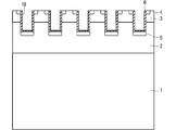
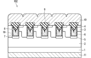
- FIG. 1 is a cross-sectional view showing a cell structure of a main part of the SiC-MOSFET 101.
- the SiC-MOSFET 101 is a power semiconductor device of the first embodiment having a trench gate structure.
- the five cell structures are shown in FIG. 1, the number of cells of the SiC-MOSFET 101 is not limited to this. Actually, the cell structure shown in FIG. 1 is continuous in an arbitrary number in the horizontal direction of the paper surface.
- the SiC-MOSFET 101 includes an n-type SiC substrate 1, an n-type SiC drift layer 2, a p-type base region 3, an n-type source region 4, a p-type bottom base region 5, a gate insulating film 6, and a gate. It includes an electrode 7, an oxide film 8, an interlayer insulating film 9, a source electrode 10, and a drain electrode 11.
- the main surface on the upper side of the paper surface of the SiC substrate 1 is referred to as the first main surface (hereinafter, also referred to as “front surface”), and the main surface on the lower side of the paper surface is referred to as the second main surface (hereinafter, also referred to as “back surface”). ).
- the drift layer 2 epitaxially grows on the first main surface of the SiC substrate 1.
- the base region 3 is selectively formed as the first impurity region on the surface layer of the drift layer 2.
- a source region 4 is selectively formed as a second impurity region on the surface layer of the base region 3. From the surface of the source region 4, a trench 19 having a depth that penetrates the source region 4 and the base region 3 and reaches the drift layer 2 is formed.
- a bottom base region 5 is formed as a third impurity region in the drift layer 2 at the bottom of the trench 19.
- a gate insulating film 6 is formed on the inner wall of the trench 19.
- a gate electrode 7 is formed inside the trench 19. The upper surface of the gate electrode 7 is covered with the oxide film 8.
- An interlayer insulating film 9 is formed on the upper part of the oxide film 8 and the upper part of the source region 4.
- a source electrode 10 is formed on the base region 3, the source region 4, and the interlayer insulating film 9.
- a drain electrode 11 is formed on the second main surface of the SiC substrate 1.
- the bottom base region 5 is not limited to the one provided in contact with the bottom of the trench 19, and may be provided in the drift layer 2 below the bottom of the trench 19. Further, the bottom base region 5 is not limited to covering the entire bottom of the trench 19, and may be provided so as to cover at least a part of the bottom of the trench 19. For example, the bottom base region 5 may be periodically arranged at intervals along the stretching direction of the trench 19, or may be provided so as to cover about half of the bottom of the trench 19 in a cross section orthogonal to the stretching direction. It may be. Alternatively, the bottom base region 5 may be configured so that the width of the bottom base region 5 is larger than the width of the trench 19 by covering the entire bottom so as to protrude in the width direction of the trench 19.
- the bottom base region 5 is not limited to the one provided along the stretching direction of the trench 19, and a plurality of bottom base regions 5 are stretched in a direction orthogonal to the stretching direction of the trench 19 to partially provide the bottom of the trench 19 in the stretching direction. May be periodically covered.
- the bottom base region 5 may be provided between the adjacent trenches 19 in the drift layer 2 in parallel with the extending direction of the trench 19.
- the bottom base region 5 is not limited to being provided linearly and continuously, and may be provided periodically at intervals in the extending direction of the trench 19.
- the formation position of the bottom base region 5 may be such that the depth of the drift layer 2 from the outermost layer is the same as the depth of the bottom of the trench 19, and may be shallow or deep.
- FIG. 2 is a flowchart showing a manufacturing process of SiC-MOSFET 101.
- the manufacturing process of the SiC-MOSFET 101 will be described along with the flow of FIG.
- the n-type SiC substrate 1 is prepared (step S1).
- a drift layer 2 made of n-type SiC is formed as an epitaxial film on the front surface of the SiC substrate 1.
- a mask (not shown) made of a resist or the like is formed on the drift layer 2, and p-type impurities are ion-implanted into the drift layer 2 through the opening of the mask.
- a p-type base region 3 is formed on the surface layer of the drift layer 2 (step S2).
- the p-type impurity is, for example, boron (B) or aluminum (Al).
- n-type impurities are ion-implanted into the base region 3 from the opening of the mask.
- a mask (not shown) made of a resist or the like is formed on the base region 3, and n-type impurities are ion-implanted into the base region 3 from the opening of the mask.
- an n-type source region 4 is selectively formed on the surface layer of the base region 3 (step S3).
- the fact that the source region 4 is selectively formed on the surface layer of the base region 3 means that there is a portion of the surface layer of the base region 3 in which the source region 4 is formed and a portion in which the source region 4 is not formed.
- n-type impurities include phosphorus (P) and nitrogen (N).
- the SiC wafer is heat-treated at a high temperature by a heat treatment device (not shown).
- a heat treatment device not shown.
- the p-type impurities and n-type impurities injected into the base region 3 and the source region 4 are electrically activated.
- a mask (not shown) made of resist or the like is formed on the surfaces of the base region 3 and the source region 4.
- the trench 19 is formed as shown in FIG. 6 by dry etching using plasma or the like (step S4).
- an oxide film made of, for example, TEOS is formed on the surfaces of the base region 3 and the source region 4, and the oxide film is used as a resist mask. It may be dry-etched by. This makes it possible to form a deep trench 19.
- p-type impurities are ion-implanted into the bottom of the trench 19.
- a p-shaped bottom base region 5 is formed at the bottom of the trench 19.
- the bottom base region 5 serves to relax the electric field at the bottom of the trench gate.
- the p-type impurity is, for example, boron (B) or aluminum (Al).
- the inner wall of the trench 19 and the surfaces of the base region 3 and the source region 4 are oxidized using a thermal oxidation method.
- the thicker the layer to be oxidized the more plasma damage can be removed, but the base region 3 and the source region 4 are reduced by that amount. Therefore, the thickness of the layer to be oxidized is 20 nm or more and 80 nm or less, more preferably 30 nm or more and 70 nm or less.
- a gate insulating film 6 is formed on the inner wall of the trench 19 by a deposition method such as chemical vapor deposition or a thermal oxidation method (step S5).
- the gate insulating film 6 is formed on the side surface and the bottom surface of the trench 19.
- the gate insulating film 6 on the bottom surface of the trench 19 has a thickness equal to or greater than that of the gate insulating film 6 on the side surface of the trench 19, and is preferably 10% or more thick.
- a gate electrode 7 made of polysilicon is formed on the gate insulating film 6. Then, as shown in FIG. 10, the surplus gate electrode 7 other than the inside of the trench 19 is removed, and the gate electrode 7 is patterned (step S6). It is desirable to use isotropic etching for patterning the gate electrode 7. For example, in the case of dry etching, etching with plasma generated using a gas containing sulfur hexafluoride (SF6) is desirable, and in the case of wet etching, etching with a mixed acid containing hydrofluoric acid and nitric acid is desirable. By these etchings, a V-shaped groove 7a can be formed on the upper surface of the gate electrode 7.
- SF6 sulfur hexafluoride
- an oxide film 8 is formed on the upper surface of the gate electrode 7 including the V-shaped groove 7a by the thermal oxidation method.
- the oxidation temperature at the time of forming the oxide film 8 is preferably 850 ° C. or higher and 1050 ° C. or lower, and more preferably 900 ° C. or higher and 1000 ° C. or lower.
- the thickness of the oxide film 8 is preferably 10 nm or more and 40 nm or less, and more preferably 20 nm or more and 35 nm or less.
- the interlayer insulating film 9 is formed on the base region 3, the source region 4, and the oxide film 8 by using a CVD (chemical vapor deposition) method. Then, the interlayer insulating film 9 is patterned by photoengraving and etching treatment, and as shown in FIG. 12, the interlayer insulating film 9 is left only on the upper part of the oxide film 8 and the source region 4 (step S7). It is also possible to round the corners of the interlayer insulating film 9 by introducing an impurity such as B (boron) or P (phosphorus).
- the material of the interlayer insulating film 9 deposited by the CVD method is, for example, silicon nitride (SixNy) or silicon oxide (SiO2).
- the thickness of the interlayer insulating film 9 is preferably 0.5 ⁇ m or more and 2.0 ⁇ m or less.
- the source electrode 10 is formed into a film as shown in FIG. 13 (step S8).
- the material of the source electrode 10 is, for example, aluminum, an aluminum alloy composed of aluminum and silicon, nickel, or the like.
- a barrier metal made of titanium or a titanium compound such as titanium nitride (TiN) may be appropriately formed between the base region 3 and the source region 4 and the source electrode 10.
- step S9 the back surface of the SiC substrate 1 is ground with a grinding wheel to thin the SiC substrate 1 (step S9).
- a nickel film having a thickness of about 600 nm is formed on the back surface of the SiC substrate 1 as the drain electrode 11 by a sputtering method or the like (step S10).
- a metal that is difficult to oxidize such as gold or silver, can be formed on the surface of the nickel film as a protective film, and a laminated film composed of the nickel film and the protective film can be used as the drain electrode 11.
- the SiC-MOSFET 101 shown in FIG. 1 is completed.
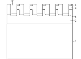
- FIG. 14 is an enlarged cross-sectional view of the trench gate of the SiC-MOSFET 101 and its surroundings.
- the y-axis is taken in the thickness direction of the SiC-MOSFET 101
- the z-axis is taken in the width direction of the trench 19
- the x-axis is taken in the direction perpendicular to the yz plane.
- a V-shaped groove 7a is formed on the upper surface of the gate electrode 7.
- the groove 7a is formed when the excess portion of the gate electrode 7 is removed by isotropic etching.
- Let ⁇ be the angle of the side surface of the groove 7a with respect to the thickness direction (z direction) of the SiC-MOSFET 101.
- ⁇ is the angle at which the vertical direction (z direction) of the paper surface of FIG. 14 intersects with the straight line drawn along the side surface of the groove 7a.
- d be the depth of the groove 7a.
- d is the distance between two midpoints adjacent to the groove 7a on the upper surface of the gate electrode 7 and the bottom of the groove 7a.
- t be the depth of the gate electrode 7.
- t is the distance between two midpoints adjacent to the groove 7a on the upper surface of the gate electrode 7 and the bottom of the gate electrode 7.
- the side surface of the trench 19 in contact with the source region 4 becomes a curved shape bulging outward.
- the outer surface of the gate electrode 7 also has a curved shape in which the portion facing the source region 4 bulges outward along the shape of the side surface of the trench 19.
- the width of the portion of the gate electrode 7 facing the source region 4 increases from the upper surface of the gate electrode 7 in the depth direction, and then decreases again.
- the side surface of the gate electrode 7 has a convex portion in a portion facing the source region 4. At this portion, an anchor effect in the z direction is generated between the gate electrode 7 and the side surface of the trench 19.
- the gate electrode 7 and the trench 19 are compared with each other as compared with the case where the outer surface of the gate electrode 7 is straight.
- the joint strength is improved to each stage.
- the gate insulating film 6 on the side surface of the gate electrode 7 is formed thicker than the gate insulating film 6 on the bottom of the gate electrode 7.
- FIG. 15 is a photomicrograph showing a cross section of SiC-MOSFET 101.
- FIG. 16 is a top view of the SiC-MOSFET 101.
- FIG. 17 is a cross-sectional view taken along the line AA'of FIG. As shown in FIG. 16, there is a terminal region 12 outside the source electrode 10, and a terminal protective film 13 outside the terminal region 12. A part of the upper surface of the SiC-MOSFET 101 becomes the gate connecting portion 14.
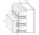
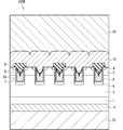
- FIG. 18 shows the semiconductor module 110 of the first embodiment.
- the semiconductor module 110 includes a SiC-MOSFET 101, lead frames 15, 17, wires 18, solder 16, and a mold resin (not shown).
- the lead frame 17 is connected to the surface of the SiC-MOSFET 101 with a wire 18.
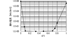
- the lead frame 15 is connected to the back surface of the SiC-MOSFET 101 with solder 16. After that, the SiC-MOSFET 101 and the lead frames 15 and 17 are sealed with the mold resin to complete the semiconductor module 110.
- FIG. 19 shows the leakage current between the gate electrode 7 and the source electrode 10 after assembling the semiconductor module 110 and d / t when the load when connecting the wire 18 to the SiC-MOSFET 101 is intentionally increased. Shows the relationship. As described above, d represents the depth of the groove 7a of the gate electrode 7, and t represents the depth of the gate electrode 7. According to FIG. 19, it is desirable that the depth d of the groove 7a is 10% or more and 70% or less of the depth t of the gate electrode 7. According to the inventor's analysis, when d is less than 10% of t, the gate electrode 7 moves in the x direction in FIG. 14 and breaks due to the stress when connecting the wire 18 to the SiC-MOSET 101. I found out. Further, when d exceeds 70% of t, it was found that the gate electrode 7 was broken starting from the groove 7a due to the stress when connecting the wire 18 to the SiC-MOSET 101.
- the wire 18 is bonded to the upper surface of the SiC-MOSFET 101, that is, a plane perpendicular to the depth direction (y-axis direction of FIG. 14) of the trench 19 (xz plane of FIG. 14).
- the direction of the wire 18 is not parallel to the plane (yz plane of FIG. 14) consisting of the depth direction of the trench 19 (y-axis direction of FIG. 14) and the width direction of the trench 19 (z-axis direction of FIG. 14)
- the effect of the characteristic trench gate structure of the SiC-MOSFET 101 can be obtained.
- the angle formed by the wire 18 and the trench 19 in the depth direction is 60 degrees or less, the effect of the characteristic trench gate structure of the SiC-MOSFET 101 can be remarkably obtained.
- FIG. 20 shows the relationship between the leakage current between the gate electrode 7 and the source electrode 10 after assembling the semiconductor module 110 and ⁇ .
- ⁇ is the angle formed by the thickness direction (z direction) of the SiC-MOSFET 101 and the side surface of the groove 7a.
- ⁇ is 1 degree or more and 20 degrees or less.
- the gate electrode 7 cracks from the groove 7a toward the lower side of the paper surface due to the stress when connecting the wire 18 to the SiC-MOSFET 101. Has progressed and it has been confirmed that it has been destroyed. Further, when ⁇ exceeds 20 degrees, it was found that the gate electrode 7 was destroyed by moving in the x direction in FIG. 14 due to the stress when connecting the wire 18 to the SiC-MOSFET 101.
- the conductive type of each semiconductor layer of the SiC-MOSFET 101 is clearly described as n-type or p-type.
- the conductive type of each semiconductor layer may be inverted. That is, in the above, the conductive type of the SiC substrate 1, the drift layer 2, and the source region 4 is n-type, and the conductive type of the base region 3 and the bottom base region 5 is p-type, but these are opposite conductive types. Is also good.
- the SiC-MOSFET 101 of the first embodiment is formed on the SiC substrate 1, the first conductive type drift layer 2 formed on the SiC substrate 1, and the first surface layer of the drift layer.
- the base region 3 which is the first impurity region of the second conductive type different from the conductive type
- the source region 4 which is the second impurity region of the first conductive type formed on the surface layer of the first impurity region, and the first impurity region.
- a gate electrode 7 that is embedded in the trench 19 and has a V-shaped groove 7a on the upper surface, and a groove 7a of the gate electrode 7 are included.
- An oxide film 8 formed on the upper surface thereof is provided.
- a first conductive type drift layer 2 is formed on a SiC substrate 1, and a second conductive type first, which is different from the first conductive type, is formed on the surface layer of the drift layer 2.
- a base region 3 which is an impurity region is formed, a source region 4 which is a first conductive type second impurity region is formed on the surface layer of the first impurity region, and drifts through the first impurity region and the second impurity region.
- a trench 19 reaching the layer 2 is formed, a gate electrode 7 having a V-shaped groove 7a on the upper surface is formed in the trench 19, and an oxide film 8 is formed on the upper surface including the groove 7a of the gate electrode 7.
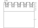
- FIG. 21 is a cross-sectional view showing a cell structure of a main part of the SiC-MOSFET 102.
- the SiC-MOSFET 102 is a power semiconductor device of the second embodiment having a trench gate structure.
- FIG. 21 shows five cell structures, the number of cells of the SiC-MOSFET 102 is not limited to this. Actually, the cell structure shown in FIG. 21 is continuous in an arbitrary number in the lateral direction of the paper surface.
- the depth of the base region 3 is not constant, and there is a shallow portion and a deep portion between two adjacent gate electrodes 7.
- the shallow portion of the base region 3 is also referred to as a first region, and the deep portion is also referred to as a second region. That is, the base region 3 has a first region and a second region deeper than the first region.
- the source region 4 overlaps the entire first region and a part of the second region.
- the second region of the base region 3 contacts the bottom base region 5.
- the SiC-MOSFET 102 is similar to the SiC-MOSFET 101 except for the depth of the base region 3.
- step S2 The manufacturing process of the SiC-MOSFET 102 is as shown in FIG. Since the step of forming the base region 3 (step S2) and the step of forming the source region 4 (step S3) are different from those of the first embodiment, they will be described below.
- the p-type base region 3 is formed on the surface layer of the drift layer 2. (Step S2).
- a shallow base region 3 and a deep base region 3 are formed.
- a mask (not shown) made of a resist or the like is formed on the base region 3, and an n-type impurity is ion-implanted into the base region 3 through the opening of the mask to form an n-type source on the surface layer of the base region 3.
- Region 4 is selectively formed (step S3).
- the source region 4 overlaps the entire shallow region of the base region 3 and a part of the deep region in a plan view.
- the base region 3 and the source region 4 are activated to form the trench 19, and the bottom base region 5 is formed at the bottom of the trench 19 as shown in FIG. 23.
- the gate insulating film 6, the gate electrode 7, the interlayer insulating film 9, the source electrode 10 and the drain electrode 11 are formed in the same manner as in the first embodiment, and the SiC-MOSFET 102 shown in FIG. 21 is completed.
- FIG. 24 is an enlarged cross-sectional view of the trench gate of the SiC-MOSFET 102 and its surroundings. According to the trench gate structure of the SiC-MOSFET 102, the following effects can be obtained in addition to the effects of the trench gate structure of the SiC-MOSFET 101.
- the base region 3 which is the first impurity region has a first region and a second region deeper than the first region.
- the SiC-MOSFET 102 on the left side of the gate electrode 7, the second region of the base region 3 is in contact with the bottom base region 5, which is the third impurity region. As a result, the source electrode 10 and the p-type bottom base region 5 are electrically connected through the p-type base region 3. Therefore, even when a high electric field is applied to the bottom base region 5 due to switching or the like, the on / off operation of the SiC-MOSFET 102 can be ensured.
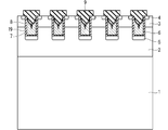
- FIG. 25 is a cross-sectional view showing the cell structure of the main part of the SiC-MOSFET 103.
- the SiC-MOSFET 103 is a power semiconductor device of the third embodiment having a trench gate structure.
- FIG. 25 shows five cell structures, the number of cells of the SiC-MOSFET 103 is not limited to this. In practice, any number of cell structures shown in FIG. 25 are continuous in the lateral direction of the paper.
- the SiC-MOSFET 103 shown in FIG. 25 includes a source electrode 20 in addition to the configuration of the SiC-MOSFET 101 shown in FIG.
- the SiC-MOSFET 103 may include a source electrode 20 in addition to the configuration of the SiC-MOSFET 102 shown in FIG.
- the source electrode 20 is formed on the source electrode 10.
- the source electrode 10 is also referred to as a first source electrode
- the source electrode 20 is also referred to as a second source electrode.
- FIG. 26 is a flowchart showing a manufacturing process of the SiC-MOSFET 103.
- a plating pretreatment step S11
- a plating treatment step S12
- FIG. 27 is a flowchart showing step S11 and step S12 shown in FIG. 26 in more detail.
- Step S11 in FIG. 26 corresponds to steps S21 to S24 in FIG.
- step S12 in FIG. 26 corresponds to steps S25 and S26 in FIG. 27.
- the source electrode 10 is made of an aluminum alloy, even if the generally known degreasing and pickling are performed, a strong organic residue and an oxide film are still present on the upper surface of the aluminum alloy. Therefore, even if the plating treatment is performed after that, metal diffusion is not sufficiently generated between the aluminum alloy and the plated metal, and a plating layer having a strong adhesive force cannot be formed. Therefore, in step S11, the upper surface of the source electrode 10 is pre-plated before the plating.
- the plating pretreatment is as follows. First, the surface activation treatment is performed in step S21.
- the surface activation treatment is carried out using, for example, plasma.
- plasma cleaning cleans the upper surface of the source electrode 10 by oxidatively decomposing organic residues that are burnt onto the upper surface of the source electrode 10 and cannot be removed by general plating pretreatment, or by knocking them out with plasma. It is possible.
- step S22 the degreasing treatment is performed in step S22.
- the degreasing treatment is performed to remove mild organic contamination or an oxide film remaining on the upper surface of the source electrode 10.
- step S23 acid cleaning is performed in step S23.
- the acid cleaning neutralizes the upper surface of the source electrode 10 and roughens it by etching.
- the acid cleaning enhances the reactivity of the treatment liquid in the subsequent process and improves the adhesive force of the plating film.
- the zincate treatment is a treatment for forming a zinc (Zn) film while removing the aluminum oxide film on the upper surface of the aluminum alloy when the source electrode 10 is made of an aluminum alloy.
- the zincate treatment is a treatment for forming a zinc (Zn) film while removing the aluminum oxide film on the upper surface of the aluminum alloy when the source electrode 10 is made of an aluminum alloy.
- aluminum dissolves as ions because the standard oxidation-reduction potential of zinc is higher than that of aluminum.
- the electrons generated at this time cause zinc ions to receive electrons on the upper surface of the aluminum alloy, forming a zinc film on the upper surface of the aluminum alloy.
- the aluminum oxide film is removed.
- the zincate treatment may be performed multiple times. For example, after performing the first gyere treatment, the gyere formed by the first gyere treatment is peeled off. Then, the second zincate treatment is performed.
- Steps S24 to S27 described above are plating pretreatments. It is necessary to secure a sufficient washing time between each step from step S24 to step S27 so that the treatment liquid or residue of the previous step is not brought into the next step.
- step S12 a plating process, which is a wet film forming method, is performed. Specifically, first, electroless Ni plating is formed in step S25.
- electroless Ni plating is formed in step S25.
- an aluminum alloy in which a zinc film is formed is immersed in a non-electrolytic Ni plating solution, first, nickel is deposited on the upper surface of the aluminum alloy because the standard oxidation-reduction potential of zinc is lower than that of nickel.
- an electroless Ni plating film having a thickness of 5 ⁇ m is formed on the upper surface of the source electrode 10.
- electroless Au plating is formed in step S26.
- the replacement type electroless Au plating is formed on the upper surface of the electroless Ni plating, and utilizes the action of replacing nickel and Au by the action of a complexing agent contained in the plating solution.
- electroless Au plating is a substitution type, the reaction stops when the surface of nickel is covered with Au. Therefore, it is difficult to form a thick electroless Au plating film.
- the thickness of electroless Au plating is at most 0.1 ⁇ m, and is generally about 0.05 ⁇ m in many cases. However, when used for soldering, the thickness of Au plating is not too thin even with the above-mentioned values.
- the film formed by the electroless Ni plating and the electroless Au plating thus formed is the source electrode 20.
- FIG. 28 is a cross-sectional view showing a manufacturing process of the semiconductor module.
- the upper surface and the lower surface of the SiC-MOSFET 103 are connected to the lead frame 27 by using solder 26, respectively.
- the SiC-MOSFET 103 and a part of the lead frame 27 are sealed with the mold resin 22 so that the tip of the lead frame 27 is exposed, and the semiconductor module is completed.
- FIG. 30 is a cross-sectional view showing a cell structure of a main part of SiC-MOSFET 103A, which is a power semiconductor device of the first modification of the first modification of the third embodiment having a trench gate structure.
- the five cell structures are shown in FIG. 30, the number of cells of the SiC-MOSFET 103A is not limited to this. In practice, any number of cell structures shown in FIG. 30 are continuous in the lateral direction of the paper.
- the interlayer insulating film 9 is formed on all the gate electrodes 7 via the oxide film 8, whereas in the SiC-MOSFET 103A, the interlayer insulating film 9 is formed on some of the gate electrodes 7. Not formed.
- the SiC-MOSFET 103A is formed as follows. After forming the gate electrode 7, an interlayer insulating film 9 is formed on the base region 3, the source region 4, and the oxide film 8. Then, when the interlayer insulating film 9 is patterned by photoengraving and etching, as shown in FIG. 30, the interlayer is formed only on a part of the gate electrode 7 and the source region 4 adjacent to the part of the gate electrode 7. The insulating film 9 is left. In the SiC-MOSFET 103A, only the gate electrode 7 on which the interlayer insulating film 9 is formed is used for switching. Therefore, it is possible to control the energization performance of the SiC-MOSFET 103A by patterning the interlayer insulating film 9.
- FIG. 31 is a cross-sectional view showing the cell structure of the main part of the SiC-MOSFET 103B, which is a power semiconductor device of the second modification of the third embodiment having a trench gate structure.
- FIG. 31 shows five cell structures, the number of cells of the SiC-MOSFET 103B is not limited to this. In practice, the cell structures shown in FIG. 31 are continuous in an arbitrary number in the lateral direction of the paper surface.
- the SiC-MOSFET 103B is a SiC-MOSFET 103A in which the drain electrode 21 of the plating film is added on the drain electrode 11.
- the drain electrode 11 is also referred to as a first drain electrode
- the drain electrode 21 is also referred to as a second drain electrode.
- the drain electrode 21 can be formed at the same time as the source electrode 20 in the manufacturing process of the SiC-MOSFET 103 described in ⁇ C-2>.
- the source electrode 20 is thicker than the drain electrode 21.
- the thickness of the source electrode 20 is preferably 1.05 times or more the thickness of the drain electrode 21.
- the solder or wire that joins the SiC-MOSFET 103, or the expansion and contraction of the source electrodes 10 and 20 included in the SiC-MOSFET 103 causes the SiC substrate to be composed of SiC.
- a force in the compressive and tensile directions (hereinafter referred to as "stretching stress”) is generated between the 1 and the drift layer 2 and the gate electrode 7 made of silicon.
- the stress of expansion and contraction acting on the front surface side becomes larger than that on the back surface side of the SiC-MOSFET 103. Therefore, the stress of expansion and contraction can be received not at the bottom of the gate electrode 7 but at the upper part of the gate electrode 7 and the trench 19 where the joint strength is remarkably improved.
- the power semiconductor device of the first to third embodiments is applied to a power conversion device.
- the application of the power semiconductor device of the first to third embodiment is not limited to a specific power conversion device.
- the three-phase inverter is applied to the power of the first to third embodiments. A case where a semiconductor device is applied will be described.
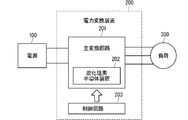
- FIG. 32 is a block diagram showing a configuration of a power conversion system to which the power conversion device of the present embodiment is applied.
- the power conversion system shown in FIG. 32 includes a power supply 100, a power conversion device 200, and a load 300.
- the power supply 100 is a DC power supply, and supplies DC power to the power converter 200.
- the power supply 100 can be configured with various things, for example, it can be configured with a DC system, a solar cell or a storage battery, or it can be configured with a rectifier circuit or an AC / DC converter connected to an AC system. May be good.
- the power supply 100 may be configured by a DC / DC converter that converts the DC power output from the DC system into a predetermined power.
- the power conversion device 200 is a three-phase inverter connected between the power supply 100 and the load 300.
- the power conversion device 200 converts the DC power supplied from the power supply 100 into AC power, and supplies the converted AC power to the load 300.
- the power conversion device 200 includes a main conversion circuit 201 and a control circuit 203.
- the main conversion circuit 201 converts the input DC power into AC power and outputs the AC power.
- the control circuit 203 outputs a control signal for controlling the main conversion circuit 201 to the main conversion circuit 201.
- the load 300 is a three-phase electric motor driven by AC power supplied from the power converter 200.
- the load 300 is not limited to a specific application, and is an electric motor mounted on various electric devices.
- the load 300 is used as an electric motor for a hybrid vehicle, an electric vehicle, a railroad vehicle, an elevator, or an air conditioner.
- the main conversion circuit 201 includes a silicon carbide semiconductor device 202.
- the silicon carbide semiconductor device 202 is a switching element and a freewheeling diode.
- the main conversion circuit 201 converts the DC power supplied from the power supply 100 into AC power, and supplies the converted AC power to the load 300.
- the main conversion circuit 201 of the present embodiment is a two-level three-phase full bridge circuit, and is opposite to the six switching elements and the respective switching elements. It can be composed of six freewheeling diodes in parallel.
- the power semiconductor device is applied to the switching element constituting the silicon carbide semiconductor device 202 of the main conversion circuit 201.
- the six switching elements are connected in series for each of the two switching elements to form an upper and lower arm, and each upper and lower arm constitutes each phase (U phase, V phase, W phase) of the full bridge circuit. Then, the output terminals of the upper and lower arms, that is, the three output terminals of the main conversion circuit 201 are connected to the load 300.
- the main conversion circuit 201 includes a drive circuit (not shown) for driving each switching element.
- the drive circuit generates a drive signal for driving the switching element of the main conversion circuit 201 and supplies the drive signal to the control electrode of the switching element of the main conversion circuit 201.
- a drive signal for turning on the switching element and a drive signal for turning off the switching element are output to the control electrodes of each switching element.
- the drive signal is a voltage signal (on signal) equal to or higher than the threshold voltage of the switching element
- the drive signal is a voltage equal to or lower than the threshold voltage of the switching element. It is a signal (off signal).
- the control circuit 203 controls the switching element of the main conversion circuit 201 so that the desired power is supplied to the load 300. Specifically, the control circuit 203 calculates the time (on time) for each switching element of the main conversion circuit 201 to be in the on state based on the electric power to be supplied to the load 300.
- the main conversion circuit 201 can be controlled by pulse width modulation (PWM) control that modulates the on-time of the switching element according to the voltage to be output.
- PWM pulse width modulation
- the control circuit 203 is driven by the main conversion circuit 201 so that an on signal is output to the switching element that should be turned on and an off signal is output to the switching element that should be turned off. Outputs a control command (control signal) to the circuit.
- the drive circuit outputs an on signal or an off signal as a drive signal to the control electrode of each switching element according to this control signal.
- the silicon carbide semiconductor device 202 described above is used as at least one of the semiconductor devices constituting the main conversion circuit 201.
- the silicon carbide semiconductor device 202 described above is used as at least one of the semiconductor devices constituting the main conversion circuit 201.
- the present embodiment has described an example in which the present disclosure is applied to a two-level three-phase inverter, the present disclosure is not limited to this, and can be applied to various power conversion devices.
- the power conversion device is a two-level power conversion device, but a multi-level power conversion device such as a three-level power conversion device may be used.
- the present disclosure when supplying power to a single-phase load, the present disclosure may be applied to a single-phase inverter.
- the present disclosure when supplying electric power to a DC load or the like, the present disclosure can be applied to a DC / DC converter or an AC / DC converter.
- the power conversion device to which the present disclosure is applied is not limited to the case where the above-mentioned load is an electric motor, and is not limited to, for example, a discharge machine, a laser machine, an induction heating cooker, or a non-contactor power supply system. It can also be used as a power supply device, and can also be used as a power conditioner for a solar power generation system, a power storage system, or the like.
Landscapes
- Engineering & Computer Science (AREA)
- Power Engineering (AREA)
- Electrodes Of Semiconductors (AREA)
Priority Applications (4)
| Application Number | Priority Date | Filing Date | Title |
|---|---|---|---|
| DE112021002411.6T DE112021002411T5 (de) | 2020-04-17 | 2021-04-14 | Leistungshalbleitergerät, Verfahren zum Herstellen eines Leistungshalbleitergeräts und Leistungswandlergerät |
| US17/796,786 US12575131B2 (en) | 2020-04-17 | 2021-04-14 | Power semiconductor device with gate having v-groove upper surface and method of manufacturing thereof |
| JP2022515408A JP7229428B2 (ja) | 2020-04-17 | 2021-04-14 | 電力用半導体装置、電力用半導体装置の製造方法および電力変換装置 |
| CN202180025233.5A CN115349177B (zh) | 2020-04-17 | 2021-04-14 | 电力用半导体装置、电力用半导体装置的制造方法及电力转换装置 |
Applications Claiming Priority (2)
| Application Number | Priority Date | Filing Date | Title |
|---|---|---|---|
| JP2020073832 | 2020-04-17 | ||
| JP2020-073832 | 2020-04-17 |
Publications (1)
| Publication Number | Publication Date |
|---|---|
| WO2021210600A1 true WO2021210600A1 (ja) | 2021-10-21 |
Family
ID=78083663
Family Applications (1)
| Application Number | Title | Priority Date | Filing Date |
|---|---|---|---|
| PCT/JP2021/015421 Ceased WO2021210600A1 (ja) | 2020-04-17 | 2021-04-14 | 電力用半導体装置、電力用半導体装置の製造方法および電力変換装置 |
Country Status (5)
| Country | Link |
|---|---|
| US (1) | US12575131B2 (https=) |
| JP (1) | JP7229428B2 (https=) |
| CN (1) | CN115349177B (https=) |
| DE (1) | DE112021002411T5 (https=) |
| WO (1) | WO2021210600A1 (https=) |
Families Citing this family (3)
| Publication number | Priority date | Publication date | Assignee | Title |
|---|---|---|---|---|
| JP7249269B2 (ja) * | 2019-12-27 | 2023-03-30 | 株式会社東芝 | 半導体装置およびその製造方法 |
| US11227926B2 (en) * | 2020-06-01 | 2022-01-18 | Nanya Technology Corporation | Semiconductor device and method for fabricating the same |
| US12610605B2 (en) * | 2022-11-28 | 2026-04-21 | Globalfoundries U.S. Inc. | IC structure with gate electrode fully within V-shaped cavity |
Citations (5)
| Publication number | Priority date | Publication date | Assignee | Title |
|---|---|---|---|---|
| JPH04290271A (ja) * | 1991-03-19 | 1992-10-14 | Nec Corp | 半導体装置 |
| JPH08505492A (ja) * | 1992-11-24 | 1996-06-11 | クリー・リサーチ・インコーポレーテッド | 炭化ケイ素におけるパワーmosfet |
| JP2017195333A (ja) * | 2016-04-22 | 2017-10-26 | 住友電気工業株式会社 | 炭化珪素半導体装置 |
| JP2017204575A (ja) * | 2016-05-12 | 2017-11-16 | 株式会社日立製作所 | パワーモジュール、電力変換装置、及びパワーモジュールの製造方法 |
| JP2019145791A (ja) * | 2018-02-16 | 2019-08-29 | インフィニオン テクノロジーズ アクチエンゲゼルシャフトInfineon Technologies AG | 炭化ケイ素から成る半導体ボディを備えた半導体装置 |
Family Cites Families (17)
| Publication number | Priority date | Publication date | Assignee | Title |
|---|---|---|---|---|
| US6133587A (en) * | 1996-01-23 | 2000-10-17 | Denso Corporation | Silicon carbide semiconductor device and process for manufacturing same |
| JPH11297714A (ja) * | 1998-04-09 | 1999-10-29 | Fujitsu Ltd | 半導体装置及びその製造方法 |
| JP4678902B2 (ja) * | 1999-09-02 | 2011-04-27 | 富士電機システムズ株式会社 | 炭化けい素umos半導体素子およびその製造方法 |
| JP4093712B2 (ja) * | 2000-10-10 | 2008-06-04 | 三洋電機株式会社 | 絶縁ゲート型半導体装置の製造方法 |
| JP2008078604A (ja) * | 2006-08-24 | 2008-04-03 | Rohm Co Ltd | Mis型電界効果トランジスタおよびその製造方法 |
| JP2009164235A (ja) * | 2007-12-28 | 2009-07-23 | Rohm Co Ltd | 窒化物半導体素子およびその製造方法 |
| JP2013125827A (ja) * | 2011-12-14 | 2013-06-24 | Toshiba Corp | 半導体装置およびその製造方法 |
| JP5884617B2 (ja) * | 2012-04-19 | 2016-03-15 | 株式会社デンソー | 炭化珪素半導体装置およびその製造方法 |
| JP2014175518A (ja) * | 2013-03-11 | 2014-09-22 | Sumitomo Electric Ind Ltd | 炭化珪素半導体装置 |
| JP2015156429A (ja) * | 2014-02-20 | 2015-08-27 | 住友電気工業株式会社 | 炭化珪素半導体装置およびその製造方法 |
| JP2016029707A (ja) * | 2014-07-24 | 2016-03-03 | 住友電気工業株式会社 | 炭化珪素半導体装置 |
| JP6623772B2 (ja) | 2016-01-13 | 2019-12-25 | 富士電機株式会社 | 炭化珪素半導体装置の製造方法 |
| CN105957892B (zh) * | 2016-04-29 | 2019-04-23 | 深圳尚阳通科技有限公司 | 屏蔽栅功率器件及其制造方法 |
| DE102017110508B4 (de) * | 2017-05-15 | 2023-03-02 | Infineon Technologies Ag | Halbleitervorrichtung mit Transistorzellen und einer Driftstruktur und Herstellungsverfahren |
| JP2019192699A (ja) * | 2018-04-19 | 2019-10-31 | 住友電気工業株式会社 | 炭化珪素半導体装置および炭化珪素半導体装置の製造方法 |
| JP7119814B2 (ja) | 2018-09-14 | 2022-08-17 | 富士電機株式会社 | 炭化珪素半導体装置および炭化珪素半導体装置の製造方法 |
| DE102018133433B4 (de) * | 2018-12-21 | 2023-07-06 | Infineon Technologies Ag | Siliziumcarbid-Körper enthaltende Halbleitervorrichtung und Herstellungsverfahren |
-
2021
- 2021-04-14 DE DE112021002411.6T patent/DE112021002411T5/de active Pending
- 2021-04-14 WO PCT/JP2021/015421 patent/WO2021210600A1/ja not_active Ceased
- 2021-04-14 US US17/796,786 patent/US12575131B2/en active Active
- 2021-04-14 JP JP2022515408A patent/JP7229428B2/ja active Active
- 2021-04-14 CN CN202180025233.5A patent/CN115349177B/zh active Active
Patent Citations (5)
| Publication number | Priority date | Publication date | Assignee | Title |
|---|---|---|---|---|
| JPH04290271A (ja) * | 1991-03-19 | 1992-10-14 | Nec Corp | 半導体装置 |
| JPH08505492A (ja) * | 1992-11-24 | 1996-06-11 | クリー・リサーチ・インコーポレーテッド | 炭化ケイ素におけるパワーmosfet |
| JP2017195333A (ja) * | 2016-04-22 | 2017-10-26 | 住友電気工業株式会社 | 炭化珪素半導体装置 |
| JP2017204575A (ja) * | 2016-05-12 | 2017-11-16 | 株式会社日立製作所 | パワーモジュール、電力変換装置、及びパワーモジュールの製造方法 |
| JP2019145791A (ja) * | 2018-02-16 | 2019-08-29 | インフィニオン テクノロジーズ アクチエンゲゼルシャフトInfineon Technologies AG | 炭化ケイ素から成る半導体ボディを備えた半導体装置 |
Also Published As
| Publication number | Publication date |
|---|---|
| CN115349177A (zh) | 2022-11-15 |
| JPWO2021210600A1 (https=) | 2021-10-21 |
| CN115349177B (zh) | 2025-10-21 |
| DE112021002411T5 (de) | 2023-02-16 |
| US20230048355A1 (en) | 2023-02-16 |
| JP7229428B2 (ja) | 2023-02-27 |
| US12575131B2 (en) | 2026-03-10 |
Similar Documents
| Publication | Publication Date | Title |
|---|---|---|
| US11984492B2 (en) | Silicon carbide semiconductor device, power converter, and method of manufacturing silicon carbide semiconductor device | |
| US11158511B2 (en) | Semiconductor device and power converter including a copper film with a small grain size stress relaxtion layer | |
| JP7229428B2 (ja) | 電力用半導体装置、電力用半導体装置の製造方法および電力変換装置 | |
| JP6947338B1 (ja) | 炭化珪素半導体装置および電力変換装置の製造方法 | |
| JP7047981B1 (ja) | 炭化珪素半導体装置および電力変換装置 | |
| US20220059688A1 (en) | Power semiconductor device and power converter | |
| CN116195070A (zh) | 碳化硅半导体装置的制造方法、碳化硅半导体装置以及电力变换装置的制造方法 | |
| US11437505B2 (en) | Semiconductor device and power conversion device | |
| US20180151709A1 (en) | Semiconductor device, substrate and electrical power conversion device | |
| JP7664872B2 (ja) | 半導体装置、電力変換装置および半導体装置の製造方法 | |
| JP7275407B1 (ja) | 炭化珪素半導体装置、電力変換装置および炭化珪素半導体装置の製造方法 | |
| JP7386662B2 (ja) | 半導体装置および電力変換装置 | |
| US20250112103A1 (en) | Semiconductor device and power converter | |
| JP2022054004A (ja) | 半導体装置の製造方法、半導体装置および電力変換装置 | |
| JP7789208B2 (ja) | 半導体装置、電力変換装置、および、半導体装置の製造方法 | |
| WO2024214501A1 (ja) | 半導体装置及び電力変換装置 | |
| WO2022097262A1 (ja) | 半導体装置および電力変換装置 | |
| WO2024214634A1 (ja) | 半導体装置及び電力変換装置 | |
| JP2025008136A (ja) | 半導体装置、半導体装置の製造方法、及び、電力変換装置 | |
| JP7529139B2 (ja) | 炭化珪素半導体装置とその製造方法、および、電力変換装置 | |
| JP2024123834A (ja) | 炭化珪素半導体装置及び電力変換装置 | |
| WO2023189164A1 (ja) | 半導体装置及び電力変換装置 | |
| JP2023158319A (ja) | 半導体装置および電力変換装置 | |
| WO2022264212A1 (ja) | 炭化珪素半導体装置および炭化珪素半導体装置を用いた電力変換装置 |
Legal Events
| Date | Code | Title | Description |
|---|---|---|---|
| 121 | Ep: the epo has been informed by wipo that ep was designated in this application |
Ref document number: 21788747 Country of ref document: EP Kind code of ref document: A1 |
|
| ENP | Entry into the national phase |
Ref document number: 2022515408 Country of ref document: JP Kind code of ref document: A |
|
| 122 | Ep: pct application non-entry in european phase |
Ref document number: 21788747 Country of ref document: EP Kind code of ref document: A1 |
|
| WWG | Wipo information: grant in national office |
Ref document number: 202180025233.5 Country of ref document: CN |
|
| WWG | Wipo information: grant in national office |
Ref document number: 17796786 Country of ref document: US |