WO2021210464A1 - アレー型半導体レーザ装置 - Google Patents
アレー型半導体レーザ装置 Download PDFInfo
- Publication number
- WO2021210464A1 WO2021210464A1 PCT/JP2021/014743 JP2021014743W WO2021210464A1 WO 2021210464 A1 WO2021210464 A1 WO 2021210464A1 JP 2021014743 W JP2021014743 W JP 2021014743W WO 2021210464 A1 WO2021210464 A1 WO 2021210464A1
- Authority
- WO
- WIPO (PCT)
- Prior art keywords
- electrode
- semiconductor laser
- conductive film
- conductor
- wiring
- Prior art date
- Legal status (The legal status is an assumption and is not a legal conclusion. Google has not performed a legal analysis and makes no representation as to the accuracy of the status listed.)
- Ceased
Links
Images


Classifications
-
- H—ELECTRICITY
- H01—ELECTRIC ELEMENTS
- H01S—DEVICES USING THE PROCESS OF LIGHT AMPLIFICATION BY STIMULATED EMISSION OF RADIATION [LASER] TO AMPLIFY OR GENERATE LIGHT; DEVICES USING STIMULATED EMISSION OF ELECTROMAGNETIC RADIATION IN WAVE RANGES OTHER THAN OPTICAL
- H01S5/00—Semiconductor lasers
- H01S5/40—Arrangement of two or more semiconductor lasers, not provided for in groups H01S5/02 - H01S5/30
- H01S5/4025—Array arrangements, e.g. constituted by discrete laser diodes or laser bar
-
- H—ELECTRICITY
- H01—ELECTRIC ELEMENTS
- H01S—DEVICES USING THE PROCESS OF LIGHT AMPLIFICATION BY STIMULATED EMISSION OF RADIATION [LASER] TO AMPLIFY OR GENERATE LIGHT; DEVICES USING STIMULATED EMISSION OF ELECTROMAGNETIC RADIATION IN WAVE RANGES OTHER THAN OPTICAL
- H01S5/00—Semiconductor lasers
- H01S5/40—Arrangement of two or more semiconductor lasers, not provided for in groups H01S5/02 - H01S5/30
- H01S5/4018—Lasers electrically in series
-
- H—ELECTRICITY
- H01—ELECTRIC ELEMENTS
- H01S—DEVICES USING THE PROCESS OF LIGHT AMPLIFICATION BY STIMULATED EMISSION OF RADIATION [LASER] TO AMPLIFY OR GENERATE LIGHT; DEVICES USING STIMULATED EMISSION OF ELECTROMAGNETIC RADIATION IN WAVE RANGES OTHER THAN OPTICAL
- H01S5/00—Semiconductor lasers
- H01S5/02—Structural details or components not essential to laser action
- H01S5/022—Mountings; Housings
- H01S5/0233—Mounting configuration of laser chips
- H01S5/0234—Up-side down mountings, e.g. Flip-chip, epi-side down mountings or junction down mountings
-
- H—ELECTRICITY
- H01—ELECTRIC ELEMENTS
- H01S—DEVICES USING THE PROCESS OF LIGHT AMPLIFICATION BY STIMULATED EMISSION OF RADIATION [LASER] TO AMPLIFY OR GENERATE LIGHT; DEVICES USING STIMULATED EMISSION OF ELECTROMAGNETIC RADIATION IN WAVE RANGES OTHER THAN OPTICAL
- H01S5/00—Semiconductor lasers
- H01S5/02—Structural details or components not essential to laser action
- H01S5/022—Mountings; Housings
- H01S5/0235—Method for mounting laser chips
- H01S5/02355—Fixing laser chips on mounts
- H01S5/0237—Fixing laser chips on mounts by soldering
-
- H—ELECTRICITY
- H01—ELECTRIC ELEMENTS
- H01S—DEVICES USING THE PROCESS OF LIGHT AMPLIFICATION BY STIMULATED EMISSION OF RADIATION [LASER] TO AMPLIFY OR GENERATE LIGHT; DEVICES USING STIMULATED EMISSION OF ELECTROMAGNETIC RADIATION IN WAVE RANGES OTHER THAN OPTICAL
- H01S5/00—Semiconductor lasers
- H01S5/04—Processes or apparatus for excitation, e.g. pumping, e.g. by electron beams
- H01S5/042—Electrical excitation ; Circuits therefor
- H01S5/0421—Electrical excitation ; Circuits therefor characterised by the semiconducting contacting layers
- H01S5/0422—Electrical excitation ; Circuits therefor characterised by the semiconducting contacting layers with n- and p-contacts on the same side of the active layer
-
- H—ELECTRICITY
- H01—ELECTRIC ELEMENTS
- H01S—DEVICES USING THE PROCESS OF LIGHT AMPLIFICATION BY STIMULATED EMISSION OF RADIATION [LASER] TO AMPLIFY OR GENERATE LIGHT; DEVICES USING STIMULATED EMISSION OF ELECTROMAGNETIC RADIATION IN WAVE RANGES OTHER THAN OPTICAL
- H01S5/00—Semiconductor lasers
- H01S5/04—Processes or apparatus for excitation, e.g. pumping, e.g. by electron beams
- H01S5/042—Electrical excitation ; Circuits therefor
- H01S5/0425—Electrodes, e.g. characterised by the structure
- H01S5/04256—Electrodes, e.g. characterised by the structure characterised by the configuration
-
- H—ELECTRICITY
- H01—ELECTRIC ELEMENTS
- H01S—DEVICES USING THE PROCESS OF LIGHT AMPLIFICATION BY STIMULATED EMISSION OF RADIATION [LASER] TO AMPLIFY OR GENERATE LIGHT; DEVICES USING STIMULATED EMISSION OF ELECTROMAGNETIC RADIATION IN WAVE RANGES OTHER THAN OPTICAL
- H01S5/00—Semiconductor lasers
- H01S5/20—Structure or shape of the semiconductor body to guide the optical wave ; Confining structures perpendicular to the optical axis, e.g. index or gain guiding, stripe geometry, broad area lasers, gain tailoring, transverse or lateral reflectors, special cladding structures, MQW barrier reflection layers
- H01S5/22—Structure or shape of the semiconductor body to guide the optical wave ; Confining structures perpendicular to the optical axis, e.g. index or gain guiding, stripe geometry, broad area lasers, gain tailoring, transverse or lateral reflectors, special cladding structures, MQW barrier reflection layers having a ridge or stripe structure
-
- H—ELECTRICITY
- H01—ELECTRIC ELEMENTS
- H01S—DEVICES USING THE PROCESS OF LIGHT AMPLIFICATION BY STIMULATED EMISSION OF RADIATION [LASER] TO AMPLIFY OR GENERATE LIGHT; DEVICES USING STIMULATED EMISSION OF ELECTROMAGNETIC RADIATION IN WAVE RANGES OTHER THAN OPTICAL
- H01S5/00—Semiconductor lasers
- H01S5/40—Arrangement of two or more semiconductor lasers, not provided for in groups H01S5/02 - H01S5/30
- H01S5/4025—Array arrangements, e.g. constituted by discrete laser diodes or laser bar
- H01S5/4031—Edge-emitting structures
-
- H—ELECTRICITY
- H01—ELECTRIC ELEMENTS
- H01S—DEVICES USING THE PROCESS OF LIGHT AMPLIFICATION BY STIMULATED EMISSION OF RADIATION [LASER] TO AMPLIFY OR GENERATE LIGHT; DEVICES USING STIMULATED EMISSION OF ELECTROMAGNETIC RADIATION IN WAVE RANGES OTHER THAN OPTICAL
- H01S2301/00—Functional characteristics
- H01S2301/17—Semiconductor lasers comprising special layers
- H01S2301/176—Specific passivation layers on surfaces other than the emission facet
-
- H—ELECTRICITY
- H01—ELECTRIC ELEMENTS
- H01S—DEVICES USING THE PROCESS OF LIGHT AMPLIFICATION BY STIMULATED EMISSION OF RADIATION [LASER] TO AMPLIFY OR GENERATE LIGHT; DEVICES USING STIMULATED EMISSION OF ELECTROMAGNETIC RADIATION IN WAVE RANGES OTHER THAN OPTICAL
- H01S5/00—Semiconductor lasers
- H01S5/02—Structural details or components not essential to laser action
- H01S5/022—Mountings; Housings
- H01S5/023—Mount members, e.g. sub-mount members
- H01S5/02315—Support members, e.g. bases or carriers
-
- H—ELECTRICITY
- H01—ELECTRIC ELEMENTS
- H01S—DEVICES USING THE PROCESS OF LIGHT AMPLIFICATION BY STIMULATED EMISSION OF RADIATION [LASER] TO AMPLIFY OR GENERATE LIGHT; DEVICES USING STIMULATED EMISSION OF ELECTROMAGNETIC RADIATION IN WAVE RANGES OTHER THAN OPTICAL
- H01S5/00—Semiconductor lasers
- H01S5/02—Structural details or components not essential to laser action
- H01S5/022—Mountings; Housings
- H01S5/0233—Mounting configuration of laser chips
- H01S5/02345—Wire-bonding
Definitions
- This disclosure relates to an array type semiconductor laser device.
- Patent Document 1 discloses a configuration in which each light emitting element region of the semiconductor laser array element is electrically connected in series. Therefore, a current is injected in series into each light emitting element region of the semiconductor laser array element disclosed in Patent Document 1. According to this, the drive current can be suppressed as compared with the case where the current is injected in parallel into each light emitting element region of the semiconductor laser array element.
- the present disclosure provides an array type semiconductor laser device in which a plurality of semiconductor laser elements are connected in series and the bias of the current flowing through the active layer is suppressed.
- the semiconductor laser apparatus is an array type semiconductor laser apparatus including a semiconductor laser array element in which a first semiconductor laser element and a second semiconductor laser element are formed on a substrate, and the first aspect thereof.
- the semiconductor laser element has a first conductive semiconductor layer from the substrate side and a first other conductive semiconductor layer, and the second semiconductor laser element has a second conductive semiconductor layer from the substrate side.
- the first semiconductor laser element has a type semiconductor layer and a second other conductive type semiconductor layer, and the first semiconductor laser element has a first waveguide extending in a first direction in the substrate surface, and the second The semiconductor laser element is arranged in a second direction in the substrate surface orthogonal to the first direction with respect to the first semiconductor laser element, and the second semiconductor laser element is the first.
- the first semiconductor laser element has a second waveguide extending in the direction of the above, and on a first surface opposite to the substrate, the first semiconductor laser element has a first electrode formed on the first other conductive semiconductor layer.
- the second semiconductor laser element On the first surface, the second semiconductor laser element has a second electrode formed on the second other conductive semiconductor layer, and on the first surface, the first semiconductor laser.
- the element is formed on the first conductive semiconductor layer, and is formed on the third electrode arranged between the first electrode and the second electrode and the first conductive semiconductor layer.
- the second semiconductor laser element is formed on the second one conductive semiconductor layer on the first surface, which has a fourth electrode arranged on the opposite side of the third electrode.
- the array-type semiconductor laser apparatus having a sixth electrode electrically connects a first conductor that electrically connects the second electrode and the third electrode, and the fifth electrode and the sixth electrode. It has a second conductor that is connected to the target.
- a plurality of semiconductor laser elements are connected in series and the bias of the light emitting point is suppressed.
- FIG. 1 is a top view showing an array type semiconductor laser device according to the first embodiment.
- FIG. 2 is a cross-sectional view showing an array type semiconductor laser device according to the first embodiment on the line II-II of FIG.
- FIG. 3 is a bottom view of the semiconductor laser array device according to the first embodiment.
- FIG. 4 is a top view showing a submount according to the first embodiment.
- FIG. 5 is a cross-sectional view showing a semiconductor laser array device according to the first embodiment in the XII-XII line of FIG.
- FIG. 6 is an enlarged view showing a region surrounded by the broken line VI of FIG.
- FIG. 7 is a cross-sectional view showing a connection portion between the semiconductor laser array element and the base according to the first embodiment.
- FIG. 1 is a top view showing an array type semiconductor laser device according to the first embodiment.
- FIG. 2 is a cross-sectional view showing an array type semiconductor laser device according to the first embodiment on the line II-II of FIG.
- FIG. 8 is a cross-sectional view showing a bonding layer between the base and the heat sink according to the first embodiment.
- FIG. 9 is a cross-sectional view showing a semiconductor laser array device according to the first modification of the first embodiment.
- FIG. 10 is an enlarged view showing a region surrounded by a broken line X in FIG.
- FIG. 11 is a top view showing an array-type semiconductor laser device according to a second modification of the first embodiment.
- FIG. 12 is a top view showing an array type semiconductor laser diode device according to a modification 3 of the first embodiment.
- FIG. 13 is a top view showing the array type semiconductor laser device according to the second embodiment.
- FIG. 14 is a top view showing the array type semiconductor laser device according to the third embodiment.
- FIG. 15 is a top view showing a submount according to the third embodiment.
- FIG. 16 is a bottom view showing the semiconductor laser array device according to the third embodiment.
- FIG. 17 is a cross-sectional view showing a semiconductor laser apparatus according to the third embodiment in the XVII-XVII line of FIG.
- FIG. 18 is a cross-sectional view showing an array-type semiconductor laser device according to a third embodiment on the XVIII-XVIII line of FIG.
- FIG. 19 is a top view showing an array-type semiconductor laser device according to a first modification of the third embodiment.
- FIG. 20 is a cross-sectional view showing an array type semiconductor laser device according to a first modification of the third embodiment in the XX-XX line of FIG.
- FIG. 20 is a cross-sectional view showing an array type semiconductor laser device according to a first modification of the third embodiment in the XX-XX line of FIG.
- FIG. 21 is a cross-sectional view showing the insulating film and the connecting film according to the first modification of the third embodiment in the XXI-XXI line of FIG.
- FIG. 22 is a cross-sectional view showing the insulating film and the connecting film according to the first modification of the third embodiment in the XXII-XXII line of FIG.
- FIG. 23 is a top view showing the array type semiconductor laser device according to the fourth embodiment.
- FIG. 24 is a cross-sectional view showing an array type semiconductor laser device according to a fourth embodiment in the XXIV-XXIV line of FIG. 23.
- FIG. 25 is a cross-sectional view showing an array type semiconductor laser device according to a fourth embodiment in the XXV-XXV line of FIG. 23.
- FIG. 26 is a top view showing a submount according to the fourth embodiment.
- FIG. 27 is a bottom view showing a submount according to the fourth embodiment.
- FIG. 28 is an enlarged view showing a region surrounded by the broken line XXVIII of FIG. 25.
- FIG. 29 is an enlarged view showing a region surrounded by the broken line XXIX of FIG. 25.
- FIG. 30 is a cross-sectional view including a second conductor of the array type semiconductor laser apparatus according to the first modification of the fourth embodiment.
- FIG. 31 is a cross-sectional view including the first conductor of the array type semiconductor laser apparatus according to the first modification of the fourth embodiment.
- FIG. 32 is a cross-sectional view including a second conductor of the array type semiconductor laser apparatus according to the second modification of the fourth embodiment.
- FIG. 33 is a cross-sectional view including the first conductor of the array type semiconductor laser apparatus according to the second modification of the fourth embodiment.
- FIG. 34 is a top view showing an array type semiconductor laser diode device according to a modification 3 of the fourth embodiment.
- FIG. 35 is a cross-sectional view showing an array type semiconductor laser device according to a modification 3 of the fourth embodiment in the XXXV-XXXV line of FIG. 34.
- FIG. 36 is a top view showing a submount according to the third modification of the fourth embodiment.
- FIG. 37 is a bottom view showing a submount according to the third modification of the fourth embodiment.
- FIG. 38 is a top view showing an array type semiconductor laser diode device according to a modification 4 of the fourth embodiment.
- FIG. 39 is a cross-sectional view showing an array type semiconductor laser device according to a modification 4 of the fourth embodiment in the XXXIX-XXXIX line of FIG. 38.
- FIG. 40 is a top view showing a submount according to the fourth modification of the fourth embodiment.
- FIG. 41 is a top view showing the array type semiconductor laser device according to the fifth embodiment.
- FIG. 42 is a top view showing the semiconductor laser array device according to the fifth embodiment.
- FIG. 43 is a cross-sectional view showing an array type semiconductor laser device according to a fifth embodiment in the XLIV-XLIV line of FIG. 41.
- FIG. 44 is a cross-sectional view showing an array-type semiconductor laser device according to a fifth embodiment on the XLIII-XLIII line of FIG. 41.
- FIG. 45 is a top view showing a submount according to the fifth embodiment.
- FIG. 46 is a bottom view showing a submount according to the fifth embodiment.
- FIG. 47 is a bottom view showing the semiconductor laser array device according to the fifth embodiment.
- FIG. 48 is a cross-sectional view showing a semiconductor laser array device according to the fifth embodiment in the XLVIII-XLVIII line of FIG. 47.
- FIG. 49 is a cross-sectional view showing a semiconductor laser array device according to the fifth embodiment in the XLIX-XLIX line of FIG. 47.
- FIG. 45 is a top view showing a submount according to the fifth embodiment.
- FIG. 46 is a bottom view showing a submount according to the fifth embodiment.
- FIG. 47 is a bottom view showing the semiconductor laser array device according to the fifth embodiment.
- FIG. 50 is an enlarged view showing a region surrounded by a broken line L in FIG. 49.
- FIG. 51 is a top view showing an array type semiconductor laser diode device according to a first modification of the fifth embodiment.
- FIG. 52 is a cross-sectional view showing an array type semiconductor laser device according to a first modification of the fifth embodiment in the LII-LII line of FIG. 51.
- FIG. 53 is a top view showing the array type semiconductor laser device according to the sixth embodiment.
- FIG. 54 is a bottom view showing the semiconductor laser array device according to the sixth embodiment.
- FIG. 55 is a cross-sectional view of the LV-LV line of FIG. 53 including the second conductor of the array type semiconductor laser device according to the sixth embodiment.
- FIG. 51 is a top view showing an array type semiconductor laser diode device according to a first modification of the fifth embodiment.
- FIG. 52 is a cross-sectional view showing an array type semiconductor laser device according to a first modification of the fifth embodiment in the LII-LII
- FIG. 56 is a cross-sectional view showing an array type semiconductor laser device according to a sixth embodiment in the LVI-LVI line of FIG. 53.
- FIG. 57 is a cross-sectional view of the LVII-LVII line of FIG. 53 including the first conductor of the array type semiconductor laser device according to the sixth embodiment.
- FIG. 58 is a bottom view showing the semiconductor laser array device according to the first modification of the sixth embodiment.
- FIG. 59 is a cross-sectional view of the LIX-LIX line of FIG. 58 including the second conductor of the semiconductor laser array element according to the first modification of the sixth embodiment.
- FIG. 60 is a cross-sectional view showing a semiconductor laser array element according to the first modification of the sixth embodiment in the LX-LX line of FIG. 58.
- FIG. 61 is a cross-sectional view of the LXI-LXI line of FIG. 58 including the first conductor of the semiconductor laser array element according to the first modification of the sixth embodiment.
- FIG. 62 is a bottom view showing the semiconductor laser array device according to the second modification of the sixth embodiment.
- FIG. 63 is a cross-sectional view of the LXIII-LXIII line of FIG. 62 including the second conductor of the semiconductor laser array element according to the second modification of the sixth embodiment.
- FIG. 64 is a cross-sectional view showing a semiconductor laser array device according to the second modification of the sixth embodiment in the LXIV-LXIV line of FIG. 62.
- FIG. 65 is a cross-sectional view of the LXV-LXV line of FIG.
- FIG. 66 is a top view showing the array type semiconductor laser device according to the seventh embodiment.
- FIG. 67 is a bottom view showing the semiconductor laser array device according to the sixth embodiment.
- FIG. 68 is a cross-sectional view showing an array-type semiconductor laser device according to a seventh embodiment on the LXVIII-LXVIII line of FIG.
- FIG. 69 is a cross-sectional view of the LXIX-LXIX line of FIG. 66 including the second conductor of the array type semiconductor laser device according to the seventh embodiment.
- FIG. 70 is a bottom view showing a semiconductor laser array device according to a modified example of the seventh embodiment.
- FIG. 71 is a cross-sectional view of the LXXI-LXXI line of FIG. 70 including the first conductor of the semiconductor laser array element according to the modified example of the seventh embodiment.
- FIG. 72 is a cross-sectional view showing a semiconductor laser array device according to a modified example of the seventh embodiment in the LXXII-LXXII line of FIG. 70.
- FIG. 73 is a top view showing the array type semiconductor laser device according to the eighth embodiment.
- FIG. 74 is a bottom view showing the semiconductor laser array device according to the eighth embodiment.
- FIG. 75 is a cross-sectional view showing an array type semiconductor laser device according to the eighth embodiment in the LXXV-LXXV line of FIG. 73.
- FIG. 76 is a cross-sectional view of the LXXVI-LXXVI line of FIG. 73 including the first conductor of the array type semiconductor laser device according to the eighth embodiment.
- FIG. 77 is a bottom view showing a semiconductor laser array device according to a modified example of the eighth embodiment.
- FIG. 78 is a cross-sectional view showing a semiconductor laser array device according to a modified example of the eighth embodiment in the line LXXVIII-LXXVIII of FIG. 77.
- FIG. 79 is a cross-sectional view showing a semiconductor laser array device according to a modification of the eighth embodiment in the LXXIX-LXXIX line of FIG. 77.
- each figure is a schematic diagram and is not necessarily exactly illustrated. Therefore, for example, the scales and the like do not always match in each figure. Further, in each figure, the same reference numerals are given to substantially the same configurations, and duplicate explanations for substantially the same configurations may be omitted or simplified.
- the terms “upper” and “lower” do not refer to the upward direction (vertically upward) and the downward direction (vertically downward) in absolute spatial recognition. Also, the terms “upper” and “lower” are used not only when the two components are spaced apart from each other and another component exists between the two components, but also when the two components It also applies when the two components are placed in close contact with each other and touch each other.
- the Z-axis positive direction will be described as “upward” and the Z-axis negative direction will be described as “downward”.
- the resonator length direction (extending direction of the waveguide) of the semiconductor laser element will be described as the Y-axis direction or the first direction. Further, the direction orthogonal to the Y-axis and the Z-axis is defined as the X-axis direction, and is also referred to as a lateral direction or a second direction.
- the "thickness” and the “height” mean the length in the Z-axis direction.
- one of the n-type and the p-type is referred to as one conductive type, and the other is referred to as the other conductive type.
- the n-type may be referred to as a monoconductive type and the p-type may be referred to as an other conductive type, but the present disclosure excludes a structure in which the n-type and the p-type are reversed. is not it.
- the array type semiconductor laser device is an array type semiconductor laser device including a plurality of semiconductor laser elements.
- an array type semiconductor laser device includes a semiconductor laser array element in which a first semiconductor laser element and a second semiconductor laser element are formed on the same substrate.
- the first semiconductor laser element has a first conductive semiconductor layer and a first other conductive semiconductor layer from the substrate side.
- the first semiconductor laser element has a first waveguide extending in a first direction in the substrate surface, and is formed on the first other conductive semiconductor layer on the first surface opposite to the substrate. It has one electrode, is formed on the first one conductive semiconductor layer on the first surface, and is between the first electrode and the second electrode (the second electrode of the second semiconductor laser element described later). It has a third electrode arranged in the above, and a fourth electrode formed on the first one conductive semiconductor layer and arranged on the opposite side of the third electrode.
- the second semiconductor laser element has a second one conductive semiconductor layer and a second other conductive semiconductor layer from the substrate side. Further, the second semiconductor laser element is arranged in a second direction in the substrate plane orthogonal to the first direction with respect to the first semiconductor laser element. Further, the second semiconductor laser device has a second waveguide extending in the first direction, and has a second electrode formed on the second other conductive semiconductor layer on the first surface. Further, the second semiconductor laser element has a fifth electrode formed on the second one conductive semiconductor layer and arranged between the third electrode and the second electrode, and a second one conductive semiconductor. It has a sixth electrode formed in a layer and arranged on the opposite side of the fifth electrode.
- the first conductor that electrically connects the second electrode and the third electrode, and the second electrode that electrically connects the fifth electrode and the sixth electrode are electrically connected. It has a conductor.
- a plurality of semiconductor laser elements included in the array type semiconductor laser device are connected in series, and one conductive type semiconductor layer and another semiconductor layer each of the first semiconductor laser element and the second semiconductor laser element have (1). More specifically, a current can be applied evenly to the waveguide or the active layer described later) in the second direction. Therefore, according to the array type semiconductor device according to the present disclosure, it is possible to suppress the bias of the light emitting points (waveguide or the active layer described later) of the first semiconductor laser device and the second semiconductor laser device.
- the Y-axis direction may be referred to as the first direction
- the X-axis direction may be referred to as the second direction.
- the side on which the semiconductor laser element outputs the laser beam is also referred to as the front, and the opposite side is also referred to as the rear.
- the positive direction of the Y-axis is also referred to as the front and the negative direction of the Y-axis is also referred to as the rear with respect to the semiconductor laser device.
- the semiconductor laser element includes a first electrode as a p electrode P10, a second electrode as a p electrode P11, a third electrode as an n electrode N11, a fourth electrode as an n electrode N10, and a fifth electrode as an n electrode N12, a sixth electrode.
- the electrode is also referred to as n electrode N13.
- the conductor that electrically connects the p-electrode P11 and the n-electrode N11 is also referred to as a first conductor.
- a conductor that electrically connects the n-electrode N12 and the n-electrode N13 is also referred to as a second conductor.
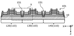
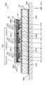
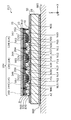
- FIG. 1 is a top view showing the array type semiconductor laser device 200 according to the first embodiment.
- FIG. 2 is a cross-sectional view showing the array type semiconductor laser device 200 according to the first embodiment on the line II-II of FIG.
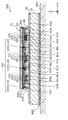
- FIG. 3 is a bottom view of the semiconductor laser array element 100 according to the first embodiment.
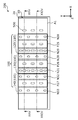
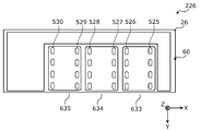
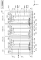
- FIG. 4 is a top view showing the submount 220 according to the first embodiment.
- FIG. 5 is a cross-sectional view showing the semiconductor laser array element 100 according to the first embodiment.
- FIG. 6 is an enlarged view showing a region surrounded by the broken line VI of FIG.
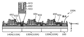
- the array-type semiconductor laser device 200 is an array-type semiconductor laser device in which the semiconductor laser element 120, the semiconductor laser element 130, and the semiconductor laser element 140 are electrically separated from each other and formed on the substrate 10.
- the semiconductor laser element 120, the semiconductor laser element 130, and the semiconductor laser element 140 are electrically separated from each other.
- each of them is said to be electrically separated from each other.
- the one conductive semiconductor layer, the active layer, and the other conductive semiconductor layer have no direct contact (in other words, are physically separated), and the semiconductor laser element 120 and the semiconductor laser element 130 (And the semiconductor laser element 130 and the semiconductor laser element 140) are shown to be electrically connected via an external wiring.
- the semiconductor laser device 120 the one conductive semiconductor layer 300 is connected to the other conductive semiconductor layer 320 via the active layer 310 without the need for external wiring.
- the semiconductor laser element 120, the semiconductor laser element 130, and the semiconductor laser element 140 are electrically connected in series in this order.
- the monoconductive semiconductor layer 300 in the semiconductor laser element 120 and the monoconductive semiconductor layer 301 in the semiconductor laser element 130 are electrically connected via the active layer 311.
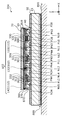
- the array type semiconductor laser device 200 includes a substrate 10, a semiconductor laser array element 100, and a base 20.
- the substrate 10 is a semiconductor substrate on which the semiconductor laser array element 100 is formed on the lower surface.
- the substrate 10 is, for example, a GaAs substrate.
- a barrier layer 810 is formed on the substrate 10.
- the barrier layer 810 is a layer having an electrical insulating property.
- the barrier layer 810 is formed between the substrate 10 and the monoconductive semiconductor layer 300, between the substrate 10 and the monoconductive semiconductor layer 301, and between the substrate 10 and the monoconductive semiconductor layer 302.
- the barrier layer 810 is, for example, an i-GaAs layer.
- the thickness L6 of the barrier layer 810 is, for example, 5 ⁇ m or more.
- the semiconductor laser array element 100 is a semiconductor laser element having a plurality of waveguides 330, 331, 332 (and light emitting points) and outputting a plurality of laser beams.
- the light emitting point is a position where the semiconductor laser array element 100 emits laser light, for example, a position of the waveguides 330 to 332 shown in FIG.
- the semiconductor laser array element 100 has a plurality of semiconductor laser elements 110.
- the semiconductor laser array element 100 includes a semiconductor laser element 120 (first semiconductor laser element), a semiconductor laser element 130 (second semiconductor laser element), and a semiconductor laser element 140 (third semiconductor laser). Element) and.
- the semiconductor laser device 120 includes an n-electrode N10, a p-electrode P10, and an n-electrode N11. Further, the semiconductor laser element 130 includes an n electrode N12, a p electrode P11, and an n electrode N13. Further, the semiconductor laser element 140 includes an n electrode N14, a p electrode P12, and an n electrode N15.
- the width of the waveguides 330 to 332 in the X-axis direction is substantially equal to the width of the p-electrodes P10 to P12 in the X-axis direction.
- the semiconductor laser element 120 When the semiconductor laser element 120, the semiconductor laser element 130, and the semiconductor laser element 140 have a common description, they are also simply referred to as the semiconductor laser element 110.
- the number of the semiconductor laser elements 110 included in the semiconductor laser array element 100 may be a plurality, and is not particularly limited. A plurality of semiconductor laser elements 110 included in the semiconductor laser array element 100 are connected in series. Therefore, the semiconductor laser element 120 and the semiconductor laser element 130 are connected in series.
- the semiconductor laser element 120 includes a monoconductive semiconductor layer 300 (first one conductive semiconductor layer), an active layer 310, and another conductive semiconductor layer 320 (first other conductive semiconductor layer) from the substrate 10 side.
- the semiconductor laser device 120 has a waveguide 330 (first waveguide) extending in the first direction (in the present embodiment, the Y-axis direction) in the surface of the substrate 10.
- the waveguide 330 is, for example, a waveguide portion of laser light composed of a part of each of the one conductive semiconductor layer 300, the active layer 310, and the other conductive semiconductor layer 320.
- the semiconductor laser element 120 has a p electrode P10 (first electrode), an n electrode N11 (third electrode), and an n electrode N10 (fourth electrode).
- the p-electrode P10 is an electrode formed so as to be electrically connected to the other conductive semiconductor layer 320 on a surface (also referred to as a lower surface or a first surface 40) located on the opposite side of the substrate 10.
- the n-electrode N11 is an electrode formed on the first surface 40 so as to be electrically connected to the monoconductive semiconductor layer 300 and arranged between the p-electrode P10 and the p-electrode P11.
- the n-electrode N10 is an electrode formed on the monoconductive semiconductor layer 300 on the first surface 40 and arranged on the side opposite to the n-electrode N11 with respect to the p-electrode P10. In other words, the p-electrode P10 is located between the n-electrode N11 and the n-electrode N10 in top view.
- the thickness L5 of the monoconductive semiconductor layer 300 between the barrier layer 810 and the n electrode N10 is, for example, 5 ⁇ m or more.
- the semiconductor laser element 120 has an insulating film 340, a protective film 350, and a wiring electrode 360.
- the insulating film 340 is a film having electrical insulating properties.
- the insulating film 340 covers the side surfaces of the semiconductor layer such as the one conductive semiconductor layer 300, the active layer 310, and the other conductive semiconductor layer 320.
- the width L7 of the insulating film 340 in the X-axis direction is, for example, 15 ⁇ m or more.
- the protective film 350 is a film that covers the insulating film 340 and protects the insulating film 340 and each semiconductor layer.
- the wiring electrode 360 is an electrode for electrically connecting the n electrodes N10, N11 and the p electrode P10 to other components such as wiring formed on the base 20.
- the thickness L8 of the wiring electrode 360 is, for example, 3 ⁇ m or more.
- the configuration of the semiconductor laser element 120 shown in FIG. 6 is the same for the semiconductor laser element 130 and the semiconductor laser element 140.
- the semiconductor laser element 130 includes a monoconductive semiconductor layer 301 (second one conductive semiconductor layer), an active layer 311 and another conductive semiconductor layer 321 (second other conductive semiconductor layer) from the substrate 10 side. Has. Further, the semiconductor laser device 130 has a waveguide 331 (second waveguide) extending in the first direction.
- the semiconductor laser element 130 has a p-electrode P11 (second electrode), an n-electrode N12 (fifth electrode), and an n-electrode N13 (sixth electrode).
- the p-electrode P11 is an electrode formed on the other conductive semiconductor layer 321 on the first surface 40.
- the n-electrode N12 is an electrode formed on the one-conductive semiconductor layer 301 on the first surface 40 and arranged between the n-electrode N11 and the p-electrode P11.
- the n-electrode N13 is an electrode formed on the monoconductive semiconductor layer 301 on the first surface 40 and arranged on the side opposite to the n-electrode N12 with respect to the p-electrode P11.
- the semiconductor laser element 140 includes a monoconductive semiconductor layer 302 (third one conductive semiconductor layer), an active layer 312, and another conductive semiconductor layer 322 (third other conductive semiconductor layer) from the substrate 10 side. Has. Further, the semiconductor laser device 140 has a waveguide 332 (third waveguide) extending in the first direction.
- the semiconductor laser element 140 has a p-electrode P12, an n-electrode N14, and an n-electrode N15.
- the p-electrode P12 is an electrode formed on the other conductive semiconductor layer 322 on the first surface 40.
- the n-electrode N14 and the n-electrode N15 are formed on the monoconductive semiconductor layer 302 on the first surface 40.
- the semiconductor laser element 130 has a second direction in the surface of the substrate 10 orthogonal to the first direction with respect to the semiconductor laser element 120 (in the present embodiment, the X-axis direction). In, they are arranged side by side.
- the n-electrode N15, p-electrode P12, n-electrode N14, n-electrode N13, p-electrode P11, n-electrode N12, n-electrode N11, p-electrode P10, and n-electrode N10 are each rectangular, in that order. They are arranged side by side in parallel in the X-axis direction. In FIG.
- the n-electrode N10 is formed of a rectangle having substantially the same shape as each of the wiring electrodes 360, and is covered with each of the wiring electrodes 360. Further, the portion where the wiring electrode 360 on the lower surface of the semiconductor laser array element 100 is not exposed is covered with the protective film 350.
- At least one of the semiconductor laser element 120 and the semiconductor laser element 130 oscillates in the horizontal multi-mode.
- the widths of the waveguides 330 and 331 are adjusted so that at least one of the semiconductor laser element 120 and the semiconductor laser element 130 oscillates in the horizontal multimode.
- the monoconductive semiconductor layer 300 and the monoconductive semiconductor layer 301 each include an n-type semiconductor layer.
- the other conductive type semiconductor layer 320 and the other conductive type semiconductor layer 321 each include a p-type semiconductor layer.
- the sub mount 220 has a pattern wiring formed on the base 20.
- the base 20 (first base) is a substrate on which the semiconductor laser array element 100 is arranged (mounted) on the upper surface (second surface 50).
- the semiconductor laser array element 100 is flip-chip mounted on the base 20.
- the p-wirings P20, P21, P22, P23 which are rectangular p-wiring in the top view, which is the conductive film on the p-side, and the upper surface, which is the conductive film on the n-side.
- U-shaped n wirings N20, N21, and N22 are formed.
- the p-wiring P21 is sandwiched between a straight portion N20a at one end and a straight portion N20b at the other end of the n-wiring N20.
- the p-wiring P22 is sandwiched between a straight portion N21a at one end and a straight portion N21b at the other end of the n-wiring N21.
- the p-wiring P23 is sandwiched between a straight portion N22a at one end and a straight portion N22b at the other end of the n-wiring N22.
- the straight portion N22a, the p wiring P23, the straight portion N22b, the straight portion N21a, the p wiring P22, the straight portion N21b, the straight portion N20a, the p wiring P21, the straight portion N20b, and the p wiring P20 are parallel in the X-axis direction in this order. Arranged side by side.
- the p-electrode and n-electrode of the semiconductor laser array element 100 are electrically connected to the pattern wiring formed on the base 20 via the wiring electrode 360 and the connection layer 370.
- the n-electrode N10 and the n-electrode N11 are electrically connected to the straight portion N20b and the straight portion N20a of the n wiring N20 via the wiring electrode 360 and the connection layer 370, respectively.
- the n-electrode N12 and the n-electrode N13 are electrically connected to the straight portion N21b and the straight portion N21a of the n-wiring N21 via the wiring electrode 360 and the connection layer 370, respectively.
- the n-electrode N14 and the n-electrode N15 are electrically connected to the straight portion N22b and the straight portion N22a of the n-wiring N22 via the wiring electrode 360 and the connection layer 370, respectively.
- the p-electrode P10 is electrically connected to the p-wiring P21 via the wiring electrode 360 and the connection layer 370.
- the p-electrode P11 is electrically connected to the p-wiring P22 via the wiring electrode 360 and the connection layer 370.
- the p-electrode P12 is electrically connected to the p-wiring P23 via the wiring electrode 360 and the connection layer 370.
- the central portion N20c of the n-wiring N20, the central portion N21c of the n-wiring N21, the central portion N22c of the n-wiring N22, one end P21a of the p-wiring P21, one end P22a of the p-wiring P22, and one end P23a of the p-wiring P23 are In the Y-axis direction, the semiconductor laser element 120 and the semiconductor laser element 130 are exposed from the rear ends (in the present embodiment, the end on the negative direction side of the Y-axis).
- the first conductive film (first conductor) and the second conductive film (second conductor) are exposed from the rear end of the semiconductor laser device 120 in the first direction.
- the second conductive film is exposed from the semiconductor laser element 120 and electrically connected to the n electrode N12 and the third portion 730, and is exposed from the semiconductor laser element 120 and electrically connected to the n electrode N13. It has a fourth portion 740 and.
- Metal wires W1 to W3 for electrically connecting each pattern wiring are formed on the second surface 50.
- the p-wiring P20 and the p-wiring P21 are electrically connected by a wire W1 joined to the p-wiring P20 and one end P21a.
- the n-wiring N20 and the p-wiring P22 are electrically connected by a wire W2 joined to the central portion N20c and one end P22a.
- the n-wiring N21 and the p-wiring P23 are electrically connected by a wire W3 joined to the central portion N21c and one end P23a.
- Each of the wires W1, W2, and W3 consists of four Au wires.
- the p-electrode P11 and the n-electrode N11 are electrically connected via the n-wiring N20, the wire W2, and the p-wiring P22.
- the n-wiring N20, the wire W2, and the p-wiring P22 are the first conductors.
- the n-electrode N12 and the n-electrode N13 are electrically connected via the n-wiring N21. That is, in the present embodiment, the n wiring N21 which is a conductive film (second conductive film) is the second conductor. Similarly, the n-electrode N10 and the n-electrode N11 are electrically connected via the n-wiring N20, and the n-electrode N14 and the n-electrode N15 are electrically connected via the n-wiring N22.
- the width of the portion of the n wiring N21 extending in the X-axis direction is, for example, 60 ⁇ m or less. Further, the length L4 (bridge wiring length) in the extending direction (that is, the X-axis direction) at the portion extending in the X-axis direction in the n wiring N21 is, for example, about 630 ⁇ m.
- the array type semiconductor laser device 200 includes a first metal wire (wire W2).
- the first metal wire (wire W2) is a metal wire that electrically connects the first portion 710 of the p-wiring P22 and the second portion 720 of the n-wiring N20.
- the first portion 710 of the p-wiring P22 points to the same region as one end P22a of the p-wiring P22 described above.
- the array type semiconductor laser device 200 has a recess 150 between the semiconductor laser element 120 and the semiconductor laser element 130.
- the recess 150 is formed in the semiconductor laser array element 100.
- the recess 150 is formed between the semiconductor laser element 120 and the semiconductor laser element 130, and is a groove for preventing the semiconductor laser element 120 and the semiconductor laser element 130 from being electrically connected without wiring or the like. be.
- the recess 150 is a groove that reaches the barrier layer 810. For example, a part of the recess 150 is also formed in the barrier layer 810.
- An insulating film 340 and a protective film 350 are formed in the recess 150.
- the semiconductor laser array element 100 is mounted on the base 20.
- the base 20 has, for example, insulating properties.
- the first surface 40 (lower surface) side of the substrate 10 is joined to the second surface 50 (upper surface) of the base 20.
- the length L2 of each of the p wirings P21, P22, and P23 in the Y-axis direction at a location that does not overlap with the semiconductor laser array element 100 is 500 ⁇ m or less.
- the semiconductor laser array element 100 and the base 20 are connected by a connecting portion 870.
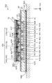
- FIG. 7 is a cross-sectional view showing a connection portion 870 according to the first embodiment.
- the wiring electrode 360 is composed of, for example, a metal layer 871 and a barrier metal layer 872 in order from the upper layer side.
- the connection layer 370 is composed of a solder layer 873 and a solder base layer 874.
- the pattern wiring (for example, n wiring N22) has an upper surface conductive layer 875 and a base layer 876.
- the base layer 876 is formed on the base 20.
- the connection layer 370 is formed in the connection region 370a shown by the dotted line on the pattern wiring.
- the metal layer 871 is made of, for example, Au.
- the metal layer 871 is formed by plating, for example.
- the barrier metal layer 872 is composed of, for example, a Pt layer and a Ti layer in order from the lower layer side.
- the solder layer 873 is made of, for example, AuSn solder.
- the solder base layer 874 is composed of, for example, a Ti layer and a Pt layer in order from the lower layer side.
- the upper surface conductive layer 875 is composed of, for example, a Cu layer, a Ni layer, and an Au layer in order from the lower layer side.
- the upper surface conductive layer 875 is formed by plating, for example.
- the base layer 876 is composed of, for example, a Ti layer, a Pt layer, and an Au layer in this order from the lower layer side, and is a layer that serves as a base when the upper surface conductive layer 875 is formed by plating.
- the base 20 is made of, for example, an insulating ceramic material such as AlN or SiC.
- the array type semiconductor laser device 200 further includes a first terminal and a second terminal.
- the first terminal is a terminal that is electrically connected to the p electrode P10.
- the first terminal is the p-wiring P20, which is the wiring formed on the base 20.
- the second terminal is a terminal that is electrically connected to the n electrode N12.
- the second terminal is the n-wiring N22, which is the wiring formed on the base 20.
- the n-electrode N12 is electrically connected to the n-wiring N22 via the n-wiring N21, the wire W3, the p-wiring P23, and the semiconductor laser element 140.
- a direct current is applied to the semiconductor laser array element 100 from an external power source (not shown) or the like via the first terminal and the second terminal.
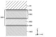
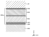
- the base 20 is placed on the heat sink 860 via the bonding layer 880.
- the heat sink 860 is formed of, for example, a metal material having high thermal conductivity such as Cu and Al.
- the heat sink 860 and the base 20 are joined by solder such as SnAgCu.
- FIG. 8 is a cross-sectional view showing the bonding layer 880 according to the first embodiment.
- the bonding layer 880 has a base layer 881, a lower surface conductive layer 882, a solder layer 883, and an upper surface conductive layer 884 in this order from the upper layer side.
- the base layer 881 is composed of, for example, an Au layer, a Pt layer, and a Ti layer in order from the lower layer side.
- the lower surface conductive layer 882 is composed of, for example, an Au layer, a Ni layer, and a Cu layer in order from the lower layer side.
- the lower surface conductive layer 882 is a layer formed by plating, for example, and in this case, the base layer 881 is a layer that serves as a base for the lower surface conductive layer 882.
- the solder layer 883 is made of, for example, SnAgCu-based low melting point solder.
- the upper surface conductive layer 884 is composed of, for example, a Ni layer and an Au layer in order from the lower layer side.
- the upper surface conductive layer 884 is, for example, a layer formed by plating.
- wiring also referred to as straddle wiring or bridge wiring
- the manufacturing process of the array type semiconductor laser device 200 can be designed more easily.
- the base 20 does not require a special process and can be easily designed.
- there are few precautions (risks) and the configuration is highly feasible.
- the p-wire P20 which is the anode electrode
- the p-wire P20 ⁇ wire W1 ⁇ p-wire P21 ⁇ p-electrode P10 ⁇ n-electrode N10, N11 ⁇ n-wire N20 ⁇ wire W2 ⁇ p wiring P22 ⁇ p electrode P11 ⁇ n electrode N12, N13 ⁇ n wiring N21 ⁇ wire W3 ⁇ p wiring P23 ⁇ p electrode P12 ⁇ n electrode N14, N15 ⁇ n wiring N22 which is a cathode electrode.
- the resonator length (length in the Y-axis direction, more specifically, length L1) of each of the plurality of semiconductor laser elements 110 is, for example, 4 mm.
- each wiring (Cu plating molding) formed on the base 20 is, for example, 75 ⁇ m at the maximum, and when combined with the connection layer 370 (thickness 5 ⁇ m or more), the thickness becomes 80 ⁇ m or more.
- the minimum distance between adjacent wirings is the plating thickness x 150%.
- the metal material used for the base 20 is, for example, Cu, Au, Al, or the like.
- the electrical wiring (wiring and wires W1, W2, W3 formed on the base 20) has a resistance value determined by the cross-sectional area and length of the electrical wiring.
- This resistance component serves as a heat generating source, and when the melting point of the wiring material is exceeded due to an overcurrent flowing or the like, the melted wiring is torn.
- the inventors of the present application melted the wire when a current of 1.4 A was passed through one Au wire (length: 3 mm) having a diameter of 25 ⁇ m. Therefore, the rated current is set to a value of about 1/3 of the fusing current calculated from the configuration of the electrical wiring (material, wiring length, and wiring cross-sectional area).
- the electrical conductivity of the material is, for example, 138% for Cu, 84% for Al, and 1% for n-GaAs.
- the array-type semiconductor laser device 200 is an array-type semiconductor laser device including a semiconductor laser array element 100 in which a semiconductor laser element 120 and a semiconductor laser element 130 are formed on a substrate 10. ..
- the semiconductor laser element 120 has one conductive semiconductor layer 300 and another conductive semiconductor layer 320 from the substrate 10 side.
- the semiconductor laser element 130 has one conductive semiconductor layer 301 and another conductive semiconductor layer 321 from the substrate 10 side.
- the semiconductor laser device 120 has a waveguide 330 extending in the first direction (Y-axis direction) in the 10 planes of the substrate.
- the semiconductor laser element 130 is arranged in a second direction (X-axis direction) in the surface of the substrate 10 orthogonal to the Y-axis direction with respect to the semiconductor laser element 120.
- the semiconductor laser device 130 has a waveguide 331 extending in the Y-axis direction.
- the semiconductor laser element 120 On the first surface 40 opposite to the substrate 10, the semiconductor laser element 120 has a first electrode (p electrode P10) formed on the other conductive semiconductor layer 320.
- the semiconductor laser element 130 has a second electrode (p electrode P11) formed on the other conductive semiconductor layer 321.
- the semiconductor laser element 120 On the first surface 40, the semiconductor laser element 120 has a third electrode (n electrode N11) formed on the one-conductive semiconductor layer 300 and arranged between the p-electrode P10 and the p-electrode P11, and one-conductivity. It has a fourth electrode (n electrode N10) formed on the type semiconductor layer 300 and arranged on opposite sides of the n electrode N11 and the p electrode P10.
- the semiconductor laser element 130 is formed on the monoconductive semiconductor layer 301, and is monoconductive with the fifth electrode (n electrode N12) arranged between the n electrode N11 and the p electrode P11.
- the array type semiconductor laser device 200 has a first conductor that electrically connects the p electrode P11 and the n electrode N11, and a second conductor that electrically connects the n electrode N12 and the n electrode N13.
- the first conductors are the p-wiring P22, the n-wiring N20, and the wire W2. Further, in the present embodiment, the second conductor is n wiring N21.
- n electrodes are arranged on both sides of the semiconductor laser element 110.
- the waveguides 330 and 331 (more specifically, the active layers 310 and 311) have a current in the center in the direction (X-axis direction) orthogonal to the extending direction of the waveguides 330 and 331 in a top view. Becomes easier to flow. Therefore, according to the array type semiconductor laser apparatus 200, a plurality of semiconductor laser elements 110 are connected in series, and the bias of the current flowing through the active layer is suppressed.
- At least one of the semiconductor laser element 120 and the semiconductor laser element 130 oscillates in the horizontal multi-mode.
- the output of the laser light from the array type semiconductor laser device 200 can be increased.
- the one-conducting semiconductor layer 300 and the one-conducting semiconductor layer 301 include an n-type semiconductor layer
- the other conductive semiconductor layer 320 and the other conductive semiconductor layer 321 include a p-type semiconductor layer.
- the conductivity of n-type semiconductors can be higher than that of p-type semiconductors.
- a current flows in the in-plane direction of the one-conductive semiconductor layer 300 and the one-conductive semiconductor layer 301.
- the resistance of the layer and the resistance of the element can be reduced, so that the resistance in the active layers 310 and 311 can be reduced in the lateral direction. It becomes easy to apply a uniform current to the current.
- the substrate 10 has an insulating property.
- the semiconductor laser element 120 and the semiconductor laser element 130 can be easily electrically separated (insulated).
- a semi-insulating GaAs substrate or a semi-insulating InP substrate may be used as the substrate 10, and the barrier layer 810 may not be formed.
- the array type semiconductor laser device 200 further has a barrier layer 810 between the substrate 10 and the monoconductive semiconductor layer 300 and between the substrate 10 and the monoconductive semiconductor layer 301, respectively.
- the semiconductor laser element 120 and the semiconductor laser element 130 can be electrically separated from each other. .. Further, even when the substrate 10 is insulating, the electrical separation between the semiconductor laser element 120 and the semiconductor laser element 130 becomes more reliable.
- the array type semiconductor laser device 200 further has a recess 150 between the semiconductor laser element 120 and the semiconductor laser element 130.
- the semiconductor laser element 120 and the semiconductor laser element 130 are electrically connected at a position not via an electrode or the like. Separation is possible.
- the first surface 40 side of the substrate 10 is joined to the second surface 50 of the base 20.
- the heat generated by the semiconductor laser element 110 can be easily dissipated to the base 20.
- the first conductor is formed on the base 20.
- the first conductor is not arranged on the first surface 40 of the array type semiconductor laser device 200, the first conductor and the second conductor of the first surface 40 of the array type semiconductor laser device 200 are arranged. Is suppressed from becoming complicated.
- the first conductor can be easily formed on the base 20.
- the first conductor is the first conductive film (p wiring P22) formed on the second surface 50.
- the p-wiring P22 is exposed from the rear end of the semiconductor laser element 120 in the Y-axis direction.
- the p-wiring P22 and the n-wiring N20 can be connected at one end P22a exposed from the rear end of the semiconductor laser element 120. Therefore, electrical insulation between the n-electrode N11 and the p-wiring P22 becomes easily possible.
- the first conductive film (p wiring P22 and n wiring N20 in the case of the first embodiment) is exposed from the semiconductor laser element 120 and the semiconductor laser element 130, and is electrically connected to the p electrode P11. It has a first portion 710 of the p-wiring P22 and a second portion 720 of the n-wiring N20 that is exposed from the semiconductor laser element 120 and the semiconductor laser element 130 and is electrically connected to the n-electrode N11. Further, the array type semiconductor laser device 200 further has a first metal wire (wire W2) that electrically connects the first portion 710 and the second portion 720.
- wire W2 first metal wire
- the first metal wire (wire W2)
- the first conductive film (n wiring N20 and p wiring P22 in the present embodiment) becomes the second conductive film (in the present embodiment).
- the p-electrode P11 and the n-electrode N11 can be connected so as not to come into contact with the n-wiring N21).
- the second conductor (n wiring N21 in the present embodiment) is formed on the base 20.
- the second conductor is not arranged on the first surface 40 of the array type semiconductor laser device 200. Therefore, it is possible to prevent the arrangement of the first conductor and the second conductor on the first surface 40 of the array type semiconductor laser device 200 from becoming complicated.
- the second conductor is a second conductive film (for example, n wiring N21) formed on the second surface 50.
- the second conductor can be easily formed on the base 20.
- the second conductive film (for example, n wiring N21) is exposed from the rear end of the semiconductor laser element 120 in the Y-axis direction.
- the fifth electrode and the sixth electrode can be connected to each other at the portion of the second conductive film exposed from the rear ends of the semiconductor laser element 120 and the semiconductor laser element 130, the second electrode and the second electrode can be connected. 2 Electrical insulation with the conductor becomes possible easily.
- the array type semiconductor laser device 200 further has a first terminal (for example, p wiring P20) connected to the p electrode P10.
- an electrical connection between an external power source (not shown) and the semiconductor laser element 110 becomes easy.
- the array type semiconductor laser device 200 further has a second terminal (for example, n wiring N22) connected to the n electrode N12.
- the electrical connection between the external power supply (not shown) and the semiconductor laser element 110 becomes easy.
- FIG. 9 is a cross-sectional view showing the semiconductor laser array element 101 according to the first modification of the first embodiment.
- FIG. 10 is an enlarged view showing a region surrounded by a broken line X in FIG.
- the semiconductor laser array element 101 has a recess 151 between the semiconductor laser element 120 and the semiconductor laser element 130.
- the recess 151 is formed between the semiconductor laser element 120 and the semiconductor laser element 130, and is a groove for preventing the semiconductor laser element 120 and the semiconductor laser element 130 from being electrically connected without wiring or the like. be.
- the recess 151 reaches, for example, the substrate 10. In other words, for example, a part of the recess 151 is also formed on the substrate 10.
- An insulating film 341 and a protective film 351 are formed in the recess 151.
- the concave portion 151 of the semiconductor laser array element 101 has a different shape from the concave portion 150 of the semiconductor laser array element 100.
- the recess 151 is formed in a tapered shape so that the width in the second direction (X-axis direction) widens from the bottom (lower side) of the recess 151 toward the opening 152 (upper side) of the recess.
- the recess 151 having such a shape can be formed by wet-etching a GaAs-based semiconductor or the like.
- the recess 151 reaches the substrate 10.
- the electrical separation between the semiconductor laser element 120 and the semiconductor laser element 130 can be made more reliable.
- the recess 151 is formed so that the width in the X-axis direction widens from the bottom of the recess 151 toward the opening 152 of the recess 151.
- the insulating film 341, the protective film 351 and the like can be uniformly formed at the corners, the side surfaces and the bottom surface of the opening 152 of the recess 151.
- FIG. 11 is a top view showing the array type semiconductor laser device 201 according to the second modification of the first embodiment.
- the array type semiconductor laser device 201 has a different wire shape from the array type semiconductor laser device 200.
- the wires W4, W5, and W6 included in the array type semiconductor laser device 201 have a curved plate shape (ribbon shape) instead of a linear shape. As described above, the shape and number of wires included in the array type semiconductor laser device 201 are not particularly limited. By thickening the wires W4, W5, and W6, the resistance can be made smaller.
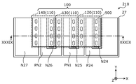
- FIG. 12 is a top view showing the array type semiconductor laser device 202 according to the third modification of the first embodiment.
- the semiconductor laser array element 100 included in the array type semiconductor laser apparatus 202 has n-electrode N10, p-electrode P10, n-electrode N11, and n-electrode N12 in order from the positive direction of the X-axis, as shown in FIG. , P electrode P11, n electrode N13, n electrode N14, p electrode P12, and n electrode N15.
- the array type semiconductor laser device 202 differs from the array type semiconductor laser device 200 in the layout of the pattern wiring formed on the base 21 (first base).
- a U-shaped p-wiring P24 in a top view, rectangular n-wirings N24 to N27 in a top view, and U-shaped pn wirings PN1 and PN2 in a top view are formed on the second surface 50 of the base 21.
- the n-wiring N24 is sandwiched between a straight portion P24a at one end of the p-wiring P24 and a straight portion P24b at the other end.
- the n-wiring N25 is sandwiched between a straight portion PN1a at one end and a straight portion PN1b at the other end of the pn wiring PN1.
- the n-wiring N26 is sandwiched between the straight portion PN2a at one end and the straight portion PN2b at the other end of the pn wiring PN2.
- the n-wiring N27, the straight portion PN2a, the n-wiring N26, the straight portion PN2b, the straight portion PN1a, the n-wiring N25, the straight portion PN1b, the straight portion P24a, the n-wiring N24, and the straight portion P24b are parallel to the X-axis direction in this order. Arranged side by side.
- the p-wiring P24 is an electrode film that is electrically connected to the p-electrode P10.
- the n-wiring N24 is an electrode film that is electrically connected to the n-electrode N10.
- the n-wiring N25 is an electrode film that is electrically connected to the n-electrode N12.
- the n-wiring N26 is an electrode film that is electrically connected to the n-electrode N14.
- the n-wiring N27 is an electrode film that is electrically connected to the n-electrode N15.
- the straight portion PN1b and the straight portion PN1a of the pn wiring PN1 are electrically connected to the n electrode N11 and the p electrode P11, respectively.
- the straight portion PN2b and the straight portion PN2a of the pn wiring PN2 are electrically connected to the n electrode N13 and the p electrode P12, respectively.
- the first conductor that electrically connects the p electrode P11 of the semiconductor laser element 130 and the n electrode N11 of the semiconductor laser element 120 is formed on the second surface 50.
- the first conductive film (first conductor) is exposed from the rear ends of the semiconductor laser element 120 and the semiconductor laser element 130 in the first direction. That is, the pn wiring PN1 has a portion on the rear end side of each of the semiconductor laser element 120 and the semiconductor laser element 130 that does not overlap with the rear end of each of the semiconductor laser element 120 and the semiconductor laser element 130 in the top view.
- the first conductive film (pn wiring PN1 in this modification) is, for example, a first portion 710 exposed from the semiconductor laser element 120 and the semiconductor laser element 130 and electrically connected to the p electrode P11, and a semiconductor laser. It has a second portion 720 that is exposed from the element 120 and the semiconductor laser element 130 and is electrically connected to the n electrode N11.
- the second conductive film (n wiring N25 and pn wiring PN2 in this modification), which is the second conductor, is exposed from the semiconductor laser element 120 and the semiconductor laser element 130, and is electrically connected to the n electrode N12. It has a third portion 730 and a fourth portion 740 that is exposed from the semiconductor laser element 120 and the semiconductor laser element 130 and is electrically connected to the n electrode N13.
- the array type semiconductor laser device 202 has a second metal wire (wire W8) that electrically connects the third portion 730 and the fourth portion 740.
- the wiring resistance between the N electrodes Since the value can be made smaller, the width of the n electrode of the semiconductor laser element 110 can be set small. Therefore, the size of the semiconductor laser array element 100 can be reduced.
- the second conductive film (n wiring N25 and pn wiring PN2) is the third portion of the n wiring N25 that is exposed from the semiconductor laser element 120 and the semiconductor laser element 130 and is electrically connected to the n electrode N12. It has a 730 and a fourth portion 740 of the pn wiring PN2 that is exposed from the semiconductor laser element 120 and the semiconductor laser element 130 and is electrically connected to the n electrode N13.
- the array type semiconductor laser device 202 further has a second metal wire (wire W8) that electrically connects the third portion 730 and the fourth portion 740.
- the n-electrode N12 and the n-electrode N13 can be connected so that the second conductive film does not come into contact with the first conductive film.
- FIG. 13 is a top view showing the array type semiconductor laser device 203 according to the second embodiment.
- the semiconductor laser array element 100 included in the array type semiconductor laser apparatus 203 has n-electrode N10, p-electrode P10, n-electrode N11, n-electrode N12, and p-electrode P11 in this order from the X-axis positive direction side.
- N electrode N13, n electrode N14, p electrode P12, and n electrode N15 are examples of the semiconductor laser array element 100 included in the array type semiconductor laser apparatus 203.
- the array type semiconductor laser device 203 has a different layout of the wiring pattern formed on the base 22 (first base) from the array type semiconductor laser device 200.
- each is rectangular in top view, n-wiring N33, p-wiring P27, n-wiring N32, n-wiring N31, p-wiring P26, n-wiring N30, n-wiring N29, p-wiring P25, The n wiring N28 and the wiring A1 are formed in this order in parallel in the X-axis direction.
- Wiring A1 is an electrode film that functions as an anode electrode.
- the wiring A1 is electrically connected to the p wiring P25 via the wire W10.
- the p-wiring P25 is an electrode film that is electrically connected to the p-electrode P10.
- the p-wiring P26 is an electrode film that is electrically connected to the p-electrode P11.
- the p-wiring P27 is an electrode film that is electrically connected to the p-electrode P12.
- the n-wiring N28 is an electrode film that is electrically connected to the n-electrode N10.
- the n-wiring N28 is electrically connected to the n-wiring N29 via the wire W11.
- the n-wiring N29 is an electrode film that is electrically connected to the n-electrode N11.
- the n-wiring N29 is electrically connected to the p-wiring P26 via the wire W12.
- the n-wiring N30 is an electrode film that is electrically connected to the n-electrode N12.
- the n-wiring N30 is electrically connected to the n-wiring N31 via the wire W13.
- the n-wiring N31 is an electrode film that is electrically connected to the n-electrode N13.
- the n-wiring N31 is electrically connected to the p-wiring P27 via the wire W14.
- the n-wiring N32 is an electrode film that is electrically connected to the n-electrode N14.
- the n-wiring N32 is electrically connected to the n-wiring N33 via the wire W15.
- the n-wiring N33 is an electrode film that is electrically connected to the n-electrode N15.
- the n-wiring N33 functions as a cathode electrode.
- n-wiring N33, p-wiring P27, n-wiring N32, n-wiring N31, p-wiring P26, n-wiring N30, n-wiring N29, p-wiring P25, and n-wiring N28 on the negative Y-axis side, respectively. Is exposed from the rear end of each of the semiconductor laser element 120 and the semiconductor laser element 130 (in the present embodiment, the end on the negative direction side of the Y axis) in the Y-axis direction.
- the wires W11, W13, and W15 electrically connect the n wirings on the rear end side of the semiconductor laser element 110. It is connected.
- the p-wiring that is electrically connected to the p-electrode of the semiconductor laser element 110 is electrically connected to the n-wiring by wires W10, W12, and W14 on the rear end side of the semiconductor laser element 110.
- the array type semiconductor laser device 203 includes four wires W10 to W15, respectively. Further, the wires W10 to W15 are all made of Au, for example.
- the wiring for electrically connecting each electrode included in the semiconductor laser array element 100 may be electrically connected by an electrode film or may be electrically connected by a metal wire.
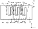
- FIG. 14 is a top view showing the array type semiconductor laser device 204 according to the third embodiment.
- FIG. 15 is a top view showing the submount 223 according to the third embodiment.
- FIG. 16 is a bottom view showing the semiconductor laser array element 102 according to the third embodiment.
- FIG. 17 is a cross-sectional view showing an array type semiconductor laser device 204 according to a third embodiment in the XVII-XVII line of FIG.
- FIG. 18 is a cross-sectional view showing an array-type semiconductor laser device 204 according to a third embodiment on the XVIII-XVIII line of FIG.
- the array type semiconductor laser device 204 includes a substrate 10, a semiconductor laser array element 102, and a base 23 (first base).
- the semiconductor laser array element 102 has a plurality of semiconductor laser elements 112.
- the semiconductor laser array element 102 includes a semiconductor laser element 122 (first semiconductor laser element), a semiconductor laser element 132 (second semiconductor laser element), and a semiconductor laser element 142 (third semiconductor laser). Element) and.
- the semiconductor laser element 122 When the semiconductor laser element 122, the semiconductor laser element 132, and the semiconductor laser element 142 have a common description, they are also simply referred to as the semiconductor laser element 112.
- the array type semiconductor laser device 204 does not have wire wiring.
- the sub mount 223 has a pattern wiring formed on the base 23.
- the semiconductor laser array element 102 is arranged (mounted) on the base 23.
- a J-shaped p-wiring P28, an N-shaped pn wiring PN3, a pn wiring PN4, and a J-shaped n-wiring N34, which are pattern wirings, are formed on the second surface 50.
- the straight portion P28a which is the shorter end of the p-wiring P28, is electrically connected to the p-electrode P10.
- the pn wiring PN3 is electrically connected to the linear portion PN3e at the end electrically connected to the n electrode N10, the linear portion PN3c at the central portion electrically connected to the n electrode N11, and the p electrode P11. It has a straight portion PN3a at the end of the wire.
- the pn wiring PN4 is electrically connected to the linear portion PN4e at the end electrically connected to the n electrode N12, the linear portion PN4c at the central portion electrically connected to the n electrode N13, and the p electrode P12.
- the n-wiring N34 has a straight portion N34c which is a shorter end electrically connected to the n-electrode N14 and a straight portion N34a which is a longer end electrically connected to the n-electrode N15. ..
- the straight portion P28a is sandwiched between the straight portion PN3c and the straight portion PN3e. Further, the straight line portion PN3a is sandwiched between the straight line portion PN4c and the straight line portion PN4e. Further, the straight line portion PN4a is sandwiched between the straight line portion N34a and the straight line portion N34c.
- the straight line portion PN3e is sandwiched between the straight line portion P28a and the straight line portion P28c. Further, the straight line portion PN4e is sandwiched between the straight line portion PN3a and the straight line portion PN3c. Further, the straight line portion N34c is sandwiched between the straight line portion PN4a and the straight line portion PN4c.
- the straight line portion N34a, the straight line portion PN4a, the straight line portion N34c, the straight line portion PN4c, the straight line portion PN3a, the straight line portion PN4e, the straight line portion PN3c, the straight line portion P28a, the straight line portion PN3e, and the straight line portion P28c are parallel to the X-axis direction in this order. Arranged side by side.
- the n electrode N10, the p electrode P10, the n electrode N11, the n electrode N12, the p electrode P11, the n electrode N13, and the n electrode N14 are arranged in this order from the positive direction side of the X axis. , P electrode P12, and n electrode N15.
- the semiconductor laser device 122 includes an n-electrode N10, a p-electrode P10, and an n-electrode N11.
- the semiconductor laser element 132 includes an n electrode N12, a p electrode P11, and an n electrode N13.
- the semiconductor laser element 142 includes an n electrode N14, a p electrode P12, and an n electrode N15.
- the n electrode N15, the p electrode P12, the n electrode N14, the n electrode N13, the p electrode P11, the n electrode N12, the n electrode N11, the p electrode P10, and the n electrode N10 are , It is formed of a rectangle having substantially the same shape as each of the wiring electrodes 360, and is covered with each of the wiring electrodes 360.
- the semiconductor laser array element 102 further includes protective films 840, 841, and 842 in addition to the configuration of the semiconductor laser array element 100.
- the protective films 840, 841, and 842 are film-like insulating films having electrical insulating properties.
- the protective film 842 is formed on a part of the wiring electrode 360 and the n electrode N10. Specifically, at the exit side end portion (the end portion on the positive direction side of the Y axis) of the wiring electrode 360 and the n electrode N10 of the semiconductor laser element 122, the connection portion P28b (straight line portion P28a) of the p wiring P28 is viewed from above. A protective film 842 is provided at a position overlapping the straight portion (the portion connecting the straight portion P28c).
- the p wiring P28 is electrically insulated from the wiring electrode 360 and the n electrode N10, and the pn wiring PN3 is electrically connected to the wiring electrode 360 and the n electrode N10.
- the protective film 841 is formed on a part of the wiring electrode 360 and the n electrode N12. Specifically, at the exit side end portion (the end portion on the positive direction side of the Y axis) of the wiring electrode 360 and the n electrode N12 of the semiconductor laser element 132, the connection portion PN3b (straight line portion PN3a) of the pn wiring PN3 is viewed from above. A protective film 841 is provided at a position overlapping the straight portion (the portion connecting the straight portion PN3c).
- the pn wiring PN3 is electrically insulated from the wiring electrode 360 and the n electrode N12, and the pn wiring PN4 is electrically connected to the wiring electrode 360 and the n electrode N12.
- the protective film 840 is formed on a part of the wiring electrode 360 and the n electrode N14. Specifically, at the exit side end portion (the end portion on the positive direction side of the Y axis) of the wiring electrode 360 and the n electrode N14 of the semiconductor laser element 142, the connection portion PN4b (straight line portion PN4a) with the pn wiring PN4 is viewed from above. A protective film 840 is provided at an overlapping position (a portion connecting the straight portion PN4c and the linear portion).
- connection portion PN3d of the pn wiring PN3 connecting the straight portion PN3c and the straight portion PN3e the connecting portion PN4d of the pn wiring PN4 connecting the straight portion PN4c and the straight portion PN4e, and n connecting the straight portion N34a and the straight portion N34c.
- the connecting portion N34b of the wiring N34 is exposed from the rear ends of the semiconductor laser element 120 and the semiconductor laser element 130 (in the present embodiment, the end on the negative direction side of the Y axis) in the Y-axis direction.
- the pn wiring PN4 is electrically insulated from the wiring electrode 360 and the n electrode N14, and the n wiring N34 and the n electrode N14 are electrically connected to each other.
- the protective films 840, 841, and 842 are integrally formed with the protective film 350 with the same material.
- connection layer 370 is formed in the connection region 370a indicated by the dotted line on the pattern wiring.
- the connection layer 370 formed on the connection portion P28b, the connection portion PN3b, and the connection portion PN4b is joined to the protective film 842, the protective film 841, and the protective film 840, respectively.
- electric power can be supplied to an appropriate position of the semiconductor laser element 112 via the pattern wiring formed on the upper surface (second surface 50) of the base 23 without using a metal wire such as a wire. ..
- the layout of the pattern wiring formed on the second surface 50 of the base 21 included in the array type semiconductor laser device 205 is the same as that of the base 21 included in the array type semiconductor laser device 202 described above.
- the pattern wiring is further electrically connected by a connecting film.
- FIG. 19 is a top view showing the array type semiconductor laser device 205 according to the first modification of the third embodiment.
- FIG. 20 is a cross-sectional view showing an array-type semiconductor laser device 205 according to a first modification of the third embodiment in the XX-XX line of FIG.
- FIG. 21 is a cross-sectional view showing the insulating films 610 to 612 and the connecting films 600 to 602 according to the first modification of the third embodiment in the XXI-XXI line of FIG.
- FIG. 22 is a cross-sectional view showing the insulating film 610 and the connecting film 600 according to the first modification of the third embodiment in the XXII-XXII line of FIG.
- the array type semiconductor laser device 205 includes a substrate 10, a semiconductor laser array element 100, and a base 21.
- the semiconductor laser array element 100 included in the array type semiconductor laser apparatus 205 has n-electrode N10, p-electrode P10, n-electrode N11, n-electrode N12, and p-electrode P11 in this order from the positive X-axis side. , N electrode N13, n electrode N14, p electrode P12, and n electrode N15.
- p wiring P24, n wirings N24 to N27, and pn wirings PN1 and PN2 are formed on the second surface 50 of the base 21.
- a film-like insulating film 610 to 612 is formed on the upper surface of the pattern wiring formed on the second surface 50 of the base 21. Further, a conductive film-like connecting film 600 to 602 is formed on the upper surface of the insulating film 610 to 612.
- connection film 600 electrically connects the n wiring N24 and the pn wiring PN1. Further, the connecting film 600 is arranged above the p-wiring P24 via the insulating film 610. As a result, the connection film 600 is electrically insulated from the p-wiring P24.
- connection film 601 electrically connects the n wiring N25 and the pn wiring PN2. Further, the connecting film 601 is arranged above the pn wiring PN1 via the insulating film 611. As a result, the connection film 601 is electrically insulated from the pn wiring PN1.
- connection film 602 electrically connects the n-wiring N26 and the n-wiring N27. Further, the connecting film 602 is arranged above the pn wiring PN2 via the insulating film 612. As a result, the connection film 602 is electrically insulated from the pn wiring PN2.
- the semiconductor laser array element 100 in each modification of the fourth embodiment and the fourth embodiment has n-electrode N10, p-electrode P10, n-electrode N11, n in order from the X-axis positive direction side.
- the electrode N12, the p electrode P11, the n electrode N13, the n electrode N14, the p electrode P12, and the n electrode N15 are provided.
- FIG. 23 is a top view showing the array type semiconductor laser device 206 according to the fourth embodiment.
- FIG. 24 is a cross-sectional view showing the array type semiconductor laser device 206 according to the fourth embodiment in the XXIV-XXIV line of FIG. 23.
- FIG. 25 is a cross-sectional view showing the array type semiconductor laser device 206 according to the fourth embodiment in the XXV-XXV line of FIG. 23.
- FIG. 26 is a top view showing the submount 224 according to the fourth embodiment.
- FIG. 27 is a bottom view showing the submount 224 according to the fourth embodiment.
- the array type semiconductor laser device 206 includes a substrate 10, a semiconductor laser array element 100, and a submount 224 (first base).
- the submount 224 has a wiring pattern and vias formed on the base 24.
- the semiconductor laser array element 100 is mounted on the base 24.
- Wiring patterns (wiring A1, p wirings P25 to P27, and n wirings N28 to N33) are formed on the second surface 50 of the base 24 in the same layout as the base 22.
- the base 24 is provided with a plurality of vias 500.
- the via 500 is a conductive electrode that penetrates the base 24 in a direction orthogonal to the second surface 50.
- the via 500 has a pattern wiring formed on the second surface 50 of the base 24 and a pattern formed on the third surface 60 opposite to the second surface 50, which is the lower surface of the base 24. Electrically connect to the wiring. That is, the via 500 penetrates from the second surface 50 to the third surface 60.
- a plurality of vias 501 to 512 are formed side by side in the Y-axis direction.
- a plurality of vias 502 and 509 are formed alternately side by side in the Y-axis direction.
- a plurality of vias 504 and 511 are formed so as to be alternately arranged in the Y-axis direction.
- the plurality of vias 500 are electrically connected to each other by the conductive film 620, respectively.
- the conductive film 620 When a common description is given for each of the conductive films 621 to 626, it is also simply referred to as a conductive film 620.
- the conductive film 620 is a conductive film formed on the third surface 60 of the base 24.
- a plurality of conductive films 620 are formed on the third surface 60 of the base 24.
- conductive films 621 to 626 are formed on the third surface 60 of the base 24.
- the conductive film 621 electrically connects the via 501 and the via 502. That is, the conductive film 621 electrically connects the n electrode N10 and the n electrode N11 of the semiconductor laser element 120. Further, for example, the conductive film 622 electrically connects the via 503 and the via 504. That is, the conductive film 622 electrically connects the n electrode N12 and the n electrode N13 of the semiconductor laser element 130. Further, for example, the conductive film 623 electrically connects the via 505 and the via 506. That is, the conductive film 623 electrically connects the n electrode N14 and the n electrode N15 of the semiconductor laser element 140.
- the conductive film 624 electrically connects the via 507 and the via 508. That is, the conductive film 624 electrically connects the p electrode P10 of the semiconductor laser element 120 and the wiring A1. Further, for example, the conductive film 625 electrically connects the via 509 and the via 510. That is, the conductive film 625 electrically connects the p electrode P11 of the semiconductor laser element 130 and the n electrode N11 of the semiconductor laser element 120. Further, for example, the conductive film 626 electrically connects the via 511 and the via 512. That is, the conductive film 626 electrically connects the p electrode P12 of the semiconductor laser element 140 and the n electrode N13 of the semiconductor laser element 130.
- the conductive films 621 to 626 extend in the X direction.
- the plurality of conductive films 624 and the plurality of conductive films 621 are formed alternately side by side in the Y-axis direction.
- the plurality of conductive films 621 and the plurality of conductive films 625 are formed alternately side by side in the Y-axis direction.
- the plurality of conductive films 625 and the plurality of conductive films 622 are formed alternately side by side in the Y-axis direction.
- the plurality of conductive films 622 and the plurality of conductive films 626 are formed alternately side by side in the Y-axis direction.
- the plurality of conductive films 626 and the plurality of conductive films 623 are formed alternately side by side in the Y-axis direction.
- the conductive film 623, the conductive film 622, and the conductive film 621 are arranged in a straight line in the X-axis direction in this order. Further, the conductive film 626, the conductive film 625, and the conductive film 624 are arranged in a straight line in the X-axis direction in this order.
- FIG. 28 is an enlarged view showing a region surrounded by the broken line XXVIII of FIG. 25.
- connection layer 370 is composed of a solder layer 891 and a solder base layer 892 in this order from the upper layer side.
- the pattern wiring (for example, n wiring N29) is composed of an upper surface conductive layer 893 and a base layer 894.
- the conductive film 620 is composed of a base layer 898 and a lower surface conductive layer 899.
- the solder layer 891 is composed of, for example, an AuSn solder layer and an Au layer in order from the lower layer side.
- the solder base layer 892 is composed of, for example, a Ti layer and a Pt layer in order from the lower layer side.
- the upper surface conductive layer 893 is composed of, for example, a Cu layer, a Ni layer, and a Pt layer in order from the lower layer side.
- the upper surface conductive layer 893 is a layer formed by plating.
- the base layer 894 is a base layer for forming the upper surface conductive layer 893 by plating, and is composed of, for example, a Ti layer, a Pt layer, and an Au layer in order from the lower layer side.
- the base 24 is, for example, an insulating substrate such as AlN or SiC.
- the via base layer 896 is composed of, for example, a Ti layer, a Pt layer, and an Au layer in order from the side wall side (X-axis positive direction side) of the via 500.
- the metal plug 897 is made of, for example, Cu formed by plating.
- the base layer 898 is, for example, a base layer for forming the metal plug 897 by plating, and is composed of an Au layer, a Pt layer, and a Ti layer in this order from the lower layer side.
- the lower surface conductive layer 899 is composed of, for example, an Au layer, a Ni layer, and a Cu layer in order from the lower layer side.
- the base 24 is placed on the heat sink 860 via the conductive film 620 and the bonding layer 880a.
- FIG. 29 is an enlarged view showing a region surrounded by the broken line XXIX of FIG. 25.
- the bonding layer 880a has a base layer 898, a lower surface conductive layer 899, a solder layer 902, an upper surface metal layer 903, and an insulating film 904 in this order from the upper layer side.
- the base layer 898 is composed of, for example, an Au layer, a Pt layer, and a Ti layer in this order from the lower layer side, and is a layer that serves as a base when the lower surface conductive layer 899 is formed by plating.
- the lower surface conductive layer 899 is composed of, for example, an Au layer, a Ni layer, and a Cu layer in order from the lower layer side.
- the lower surface conductive layer 899 is a layer formed by plating.
- the solder layer 902 is, for example, a solder made of a SnAgCu-based low melting point solder material.
- the upper surface metal layer 903 is composed of, for example, a Ti layer, a Pt layer, and an Au layer in order from the lower layer side.
- the insulating film 904 is made of, for example, a ceramic material having electrical insulation and high thermal conductivity such as AlN.
- the base 24 has a third surface 60 located on the opposite side of the second surface 50 and the second surface 50 to the third surface 60. It has a first through hole (a through hole in which a via 510 is formed) and a second through hole (a through hole in which a via 509 is formed) that penetrates from the second surface 50 to the third surface 60. ..
- the first conductor is composed of a third conductor (via 510), a fourth conductor (via 509), and a third conductive film (conductive film 625).
- the third conductive film (conductive film 625) is formed on the third surface 60.
- the third conductor (via 510) is formed in the first through hole, and electrically connects the p electrode P11 of the semiconductor laser element 130 and the third conductive film (conductive film 625).
- the fourth conductor (via 509) is formed in the second through hole, and electrically connects the n electrode N11 of the semiconductor laser element 120 and the third conductive film (conductive film 625).
- the length of the base 24 in the Y direction may be about the length of the resonator of the semiconductor laser array element 100, and the first conductivity exposed from the rear ends of the semiconductor laser element 120 and the semiconductor laser element 130, respectively.
- the area of the base 24 (the area of the second surface 50) can be reduced as compared with the case where the p electrode P11 of the semiconductor laser element 130 and the n electrode N11 of the semiconductor laser element 130 are connected. can.
- a plurality of third conductors are formed in the Y-axis direction, and a plurality of fourth conductors are formed in the Y-axis direction.
- a current can be uniformly passed through the p electrode P11 and the n electrode N11 in the first direction.
- a current can be uniformly passed through the p electrode P11 and the n electrode N11 in the first direction.
- a current flows concentrated in the p electrode P11 and the n electrode N11 in the vicinity of the first conductor.
- the current can flow uniformly in the first direction.
- a plurality of the third conductor (via 510) and the fourth conductor (via 509) are formed in the Y direction, and the total cross-sectional area of each of the third conductor and the fourth conductor becomes large.
- the rated current value can be set larger.
- the areas of the p-electrode P11 and the n-electrode N11 of the semiconductor laser array element 100 can be reduced, and the areas of the semiconductor laser array element 100 and the base 24 can be set small.
- the base 24 has a third surface 60 located on the opposite side of the second surface 50 and a fifth through hole (a penetration through which a via 503 is formed) penetrating from the second surface 50 to the third surface 60.
- the second conductor is composed of a sixth conductor (via 503), a seventh conductor (via 504), and a fourth conductive film (conductive film 622).
- the fourth conductive film (conductive film 622) is formed on the third surface 60.
- the sixth conductor (via 503) is formed in the fifth through hole, and electrically connects the n electrode N12 and the fourth conductive film (conductive film 622).
- the seventh conductor (via 504) is formed in the sixth through hole, and electrically connects the n electrode N13 and the fourth conductive film (conductive film 622).
- the length of the base 24 in the Y direction may be about the length of the resonator of the semiconductor laser array element 100, and the portion of the wiring exposed from the rear ends of the semiconductor laser element 120 and the semiconductor laser element 130, respectively. Therefore, the area of the base 24 can be reduced as compared with the case where the n-electrode N12 and the n-electrode N13 are connected.
- a plurality of sixth conductors are formed in the Y-axis direction, and a plurality of seventh conductors are formed in the Y-axis direction.
- a current can be uniformly passed through the n-electrode N12 and the n-electrode N13 in the first direction.
- a current flows concentrated in the n-electrode N12 and the n-electrode N13 in the vicinity of the second conductor.
- it is possible to suppress the problem that the current flows concentrated in the n-electrode N12 and the n-electrode N13 in the vicinity of the second conductor, and the n-electrode N12 and the n-electrode N13 are formed.
- the current can flow uniformly in the first direction.
- a plurality of the sixth conductor (via 503) and the seventh conductor (via 504) are formed side by side in the Y direction, and the total of the sixth conductor and the seventh conductor is cut off.
- the rated current value can be set larger.
- the areas of the n-electrode N12 and the n-electrode N13 of the semiconductor laser array element 100 can be reduced, and the areas of the semiconductor laser array element 100 and the base 24 can be set small.
- the base 24 has a third surface 60 located on the opposite side of the second surface 50 and a first through hole (via 510) penetrating from the second surface 50 to the third surface 60. (Through hole through which the via 509 is formed) and a second through hole (through hole in which the via 509 is formed) penetrating from the second surface 50 to the third surface 60. It is composed of a body (via 510), a fourth conductor (via 509), and a third conductive film (conductive film 625), and the third conductive film (conductive film 625) is formed on the third surface 60 and has a third conductive film.
- the body (via 510) is formed in the first through hole, the p electrode P11 and the third conductive film (conductive film 625) are electrically connected, and the fourth conductor (via 509) is formed in the second through hole.
- the n-electrode N11 and the third conductive film (conductive conductive film 625) are electrically connected to each other, and the base 24 further has a fifth through hole (a fifth through hole) penetrating from the second surface 50 to the third surface 60.
- the second conductor has a through hole (a through hole in which the via 503 is formed) and a sixth through hole (a through hole in which the via 504 is formed) penetrating from the second surface 50 to the third surface 60, and the second conductor is the sixth.
- the conductor (via 503) is formed in the fifth through hole to electrically connect the n electrode N12 and the fourth conductive film (conductive film 622), and the seventh conductor (via 504) is formed through the sixth through hole. It is formed in the pores and electrically connects the n electrode N13 and the fourth conductive film (conductive conductive film 622).
- the length of the base 24 in the Y direction may be about the length of the resonator of the semiconductor laser array element 100, and the portion of the wiring exposed from the rear ends of the semiconductor laser element 120 and the semiconductor laser element 130, respectively. Therefore, the area of the base 24 can be reduced as compared with the case where the p electrode P11 and the n electrode N11 are connected and the n electrode N12 and the n electrode N13 are connected.
- a plurality of third conductors are formed in the Y-axis direction
- a plurality of fourth conductors are formed in the Y-axis direction
- a sixth conductor is formed in the Y-axis direction.
- a plurality of seventh conductors are formed in the Y-axis direction
- a plurality of third conductive films are formed in the Y-axis direction
- a plurality of fourth conductive films are formed.
- a plurality of films 622) are formed in the Y-axis direction.
- the third conductive film (conductive film 625) and the fourth conductive film (conductive film 622) are alternately formed in the Y-axis direction.
- a current can be uniformly passed through the p electrode P11 and the n electrode N11 in the first direction. Further, a current can be uniformly passed through the n-electrode N12 and the n-electrode N13 in the first direction. For example, when there is only one first conductor, there is a problem that a current flows concentrated in the p electrode P11 and the n electrode N11 in the vicinity of the first conductor. Further, when there is only one second conductor, there arises a problem that a current flows concentrated in the n-electrode N12 and the n-electrode N13 in the vicinity of the second conductor.
- a plurality of the third conductor, the fourth conductor, the sixth conductor, and the seventh conductor are formed side by side in the Y direction, and the third conductor, the fourth conductor, and the seventh conductor are formed.
- the rated current value can be set larger by increasing the total cross-sectional area of each of the 6 conductors and the 7th conductor (for example, the area of the cross section in the XY plane).
- the electrode areas of the p-electrode P11, the n-electrode N11, the n-electrode N12, and the n-electrode N13 of the semiconductor laser array element 100 can be reduced, and the semiconductor laser array element 100 and the base 24 can be reduced.
- the area can be set small.
- FIG. 30 and 31 are cross-sectional views showing an array type semiconductor laser device 207 according to the first modification of the fourth embodiment.
- FIG. 30 is a cross-sectional view including a second conductor of the array type semiconductor laser device 207 according to the first modification of the fourth embodiment.
- FIG. 31 is a cross-sectional view including the first conductor of the array type semiconductor laser apparatus according to the first modification of the fourth embodiment.
- 30 is a diagram showing a cross section corresponding to FIG. 24, and
- FIG. 31 is a diagram showing a cross section corresponding to FIG. 25.
- the array type semiconductor laser device 207 further includes a base 30 (second base) and a bonding layer 880b in addition to the configuration of the array type semiconductor laser device 206.
- the base 30 is, for example, an insulating substrate such as AlN or SiC.
- the base 24 (first base) is placed on the base 30 via the bonding layer 880a. Further, the base 30 is placed on the heat sink 860 via the bonding layer 880b.
- the base 30 has a fifth surface 80 to which the base 24 is connected.
- the third surface 60 of the base 24 is joined to the fifth surface 80 of the base 30.
- a metal film 400 (first metal film) is formed on the fifth surface 80 so as to face the conductive film 625 (third conductive film). Further, a metal film 401 (second metal film) is formed on the fifth surface 80 so as to face the conductive film 622 (fourth conductive film).
- the metal films 400 and 401 are, for example, a part of the bonding layer 880a. As shown in FIGS. 30 and 31, the bonding layer 880a does not have to have the insulating film 904 shown in FIG. 29, for example.
- the third surface 60 is joined to the fifth surface 80 of the base 30.
- a first metal film metal film 400
- the fifth surface 80 so as to face the third conductive film (conductive film 625)
- the fourth conductive film (conductive film 622) is formed.
- a second metal film metal film 401 is formed so as to face each other.
- the heat generated by the semiconductor laser array element 100 is based on the heat generated by the semiconductor laser array element 100 via the conductive film 625, the conductive film 622, the metal film 400, and the metal film 401. Efficient heat can be dissipated from the base 24 to the base 30.
- FIG. 32 and 33 are cross-sectional views showing the array type semiconductor laser device 208 according to the second modification of the fourth embodiment.
- FIG. 32 is a cross-sectional view including a second conductor of the array type semiconductor laser apparatus 208 according to the second modification of the fourth embodiment.
- FIG. 33 is a cross-sectional view including the first conductor of the array type semiconductor laser device 208 according to the second modification of the fourth embodiment. Note that FIG. 32 is a diagram showing a cross section corresponding to FIG. 24, and FIG. 33 is a diagram showing a cross section corresponding to FIG. 25.
- conductive conductive films 627 to 632 for electrically connecting a plurality of vias 500 are formed inside the base 25 (first base).
- the array type semiconductor laser device 208 includes vias 513 to 524 that do not completely penetrate the second surface 50 to the third surface 60 of the base 25, and the base 25 is provided by the conductive film 627 to 632.
- a part of the pattern wiring formed on the second surface 50 of the above is electrically connected via the inside of the base 25.
- the conductive films 627 to 632 extend in the X direction inside the base 25.
- the conductive film 627 electrically connects the via 513 and the via 514.
- the conductive film 628 electrically connects the via 515 and the via 516.
- the conductive film 629 electrically connects the via 517 and the via 518.
- the conductive film 630 electrically connects the via 519 and the via 520.
- the conductive film 631 electrically connects the via 521 and the via 522.
- the conductive film 632 electrically connects the via 523 and the via 524.
- the n-electrode N11 and the p-electrode P11 are electrically connected via vias 521 and 522 and a conductive film 631. Further, for example, the n-electrode N12 and the n-electrode n13 are electrically connected via vias 515, 516 and a conductive film 628.
- the array type semiconductor laser device 208 can insulate the conductive films 627 to 632 by using an insulating ceramic material such as SiC or AlN as the base 25.
- the base 25 is placed on the heat sink 860 via the bonding layer 880.
- the base 25 penetrates the fifth conductor (conductive film 631) located inside the base 25 and the second surface 50 to the fifth conductor (conductive film 631). It has three through holes (through holes in which vias 522 are formed) and fourth through holes (through holes in which vias 521 are formed) that penetrate from the second surface 50 to the fifth conductor.
- the first conductor is composed of a third conductor (via 522), a fourth conductor (via 521), and a fifth conductor (conductive film 631).
- the third conductor (via 522) is formed in the third through hole, and the p electrode P11 and the fifth conductor (conductive film 631) are electrically connected.
- the fourth conductor (via 521) is formed in the fourth through hole, and the n electrode N11 and the fifth conductor (conductive film 631) are electrically connected.
- the length of the base 25 in the Y direction may be about the length of the resonator of the semiconductor laser array element 100, and the pattern wiring exposed from the rear ends of the semiconductor laser element 120 and the semiconductor laser element 130, respectively.
- the area of the base 25 can be reduced as compared with the case where the p electrode P11 and the n electrode N11 are connected.
- the base 25 has a seventh through hole penetrating the eighth conductor (conductive film 628) located inside the base 25 and the second surface 50 to the eighth conductor (conductive film 628). It has (a through hole in which the via 515 is formed) and an eighth through hole (a through hole in which the via 516 is formed) that penetrates from the second surface 50 to the eighth conductor (conductive film 628).
- the second conductor is composed of a ninth conductor (via 515), a tenth conductor (via 516), and an eighth conductor (conductive film 628).
- the ninth conductor (via 515) is formed in the seventh through hole, and electrically connects the n electrode N12 and the eighth conductor (conductive film 628).
- the tenth conductor (via 516) is formed in the second through hole, and the n electrode N13 and the eighth conductor (conductive film 628) are electrically connected.
- the length of the base 25 in the Y direction may be about the length of the resonator of the semiconductor laser array element 100, and the wiring pattern exposed from the rear ends of the semiconductor laser element 120 and the semiconductor laser element 130, respectively.
- the area of the base 25 can be reduced as compared with the case where the n-electrode N12 and the n-electrode N13 are connected.
- FIG. 34 is a top view showing the array type semiconductor laser device 209 according to the third modification of the fourth embodiment.
- FIG. 35 is a cross-sectional view showing an array type semiconductor laser device 209 according to a modification 3 of the fourth embodiment in the XXXV-XXXV line of FIG. 34.
- FIG. 36 is a top view showing the sub-mount 226 according to the third modification of the fourth embodiment.
- FIG. 37 is a bottom view showing the sub-mount 226 according to the third modification of the fourth embodiment.
- the submount 226 has a wiring pattern and vias formed on the base 26.
- the wiring pattern formed on the upper surface of the base 26 has the same layout as the base 20 shown in FIG. Specifically, conductive pattern wiring (p wiring P20, P21, P22, P23, and n wiring N20, N21, N22) is formed on the base 26.
- a plurality of vias 500 penetrating from the second surface 50 to the third surface 60 are formed on the base 26.
- vias 525 to 530 that penetrate from the second surface 50 to the third surface 60 are formed on the base 26.
- a plurality of vias 525 to 530 are formed on the base 26 side by side in the Y-axis direction.
- conductive films 633 to 635 having conductivity are formed on the third surface 60 of the base 26.
- the conductive film 633 electrically connects the via 525 and the via 526. Further, for example, the conductive film 634 electrically connects the via 527 and the via 528. Further, for example, the conductive film 635 electrically connects the via 529 and the via 530.
- the conductive film 635, the conductive film 634, and the conductive film 633 are each rectangular in top view, and are formed side by side in the X direction in this order.
- the n-electrode N11 and the p-electrode P11 are electrically connected via vias 527 and 528 and a conductive film 634. Further, for example, the n electrode N12 and the n electrode n13 are electrically connected via the n wiring N21.
- the central portion N20c of the n-wiring N20, the central portion N21c of the n-wiring N21, and the central portion N22c of the n-wiring N22 are the semiconductor laser element 110, the semiconductor laser element 120, and the semiconductor laser element 130, respectively, in the Y-axis direction. It is exposed from the rear end (in the present embodiment, the end on the negative direction side of the Y axis).
- FIG. 38 is a top view showing the array type semiconductor laser device 210 according to the fourth modification of the fourth embodiment.
- FIG. 39 is a cross-sectional view showing an array type semiconductor laser device 210 according to a modification 4 of the fourth embodiment in the XXXIX-XXXIX line of FIG. 38.
- FIG. 40 is a top view showing the sub-mount 227 according to the fourth modification of the fourth embodiment.
- the submount 227 has a wiring pattern and vias formed on the base 27.
- the wiring pattern formed on the base 27 has the same layout as the base 21. Specifically, conductive pattern wiring (p wiring P24, n wiring N24 to N27, and pn wiring PN1, PN2) is formed on the base 27.
- a plurality of vias 500 penetrating from the second surface 50 to the third surface 60 are formed on the base 27.
- vias 531 to 535 penetrating from the second surface 50 to the third surface 60 are formed on the base 27.
- a plurality of vias 531 to 536 are formed on the base 27 side by side in the Y-axis direction.
- conductive films 636 to 638 having conductivity are formed on the third surface 60 of the base 27.
- the conductive film 636 electrically connects the via 531 and the via 532. That is, the conductive film 636 electrically connects the n electrode N10 and the n electrode N11 of the semiconductor laser element 120. Further, for example, the conductive film 637 electrically connects the via 533 and the via 534. That is, the conductive film 637 electrically connects the n electrode N12 and the n electrode N13 of the semiconductor laser element 130. Further, for example, the conductive film 638 electrically connects the via 535 and the via 536. That is, the conductive film 638 electrically connects the n electrode N14 and the n electrode N15 of the semiconductor laser element 140.
- the n electrode N11 of the semiconductor laser element 120 and the p electrode P11 of the semiconductor laser element 130 are electrically connected via the pn wiring PN1. Further, for example, the n-electrode N12 and the n-electrode N13 of the semiconductor laser element 130 are electrically connected via vias 533, 534, and a conductive film 637.
- the central portion P24c of the p-wiring P24, the central portion PN1c of the pn wiring PN1, and the central portion PN2c of the pn wiring PN2 are the rear ends of the semiconductor laser element 120, the semiconductor laser element 130, and the semiconductor laser element 140 in the Y-axis direction. It is exposed from (in the present embodiment, the end on the negative side of the Y-axis).
- a plurality of semiconductor laser elements 110 may be connected in series by the via and the conductive film without using a wire.
- FIG. 41 is a top view showing the array type semiconductor laser device 211 according to the fifth embodiment.
- FIG. 42 is a top view showing the semiconductor laser array element 103 according to the fifth embodiment.
- FIG. 43 is a cross-sectional view showing the array type semiconductor laser device 211 according to the fifth embodiment in the XLIV-XLIV line of FIG. 41.
- FIG. 44 is a cross-sectional view showing the array type semiconductor laser device 211 according to the fifth embodiment on the XLIII-XLIII line of FIG. 41.
- FIG. 45 is a top view showing the submount 228 according to the fifth embodiment.
- FIG. 46 is a bottom view showing the submount 228 according to the fifth embodiment.
- FIG. 47 is a bottom view showing the semiconductor laser array element 103 according to the fifth embodiment.
- FIG. 48 is a cross-sectional view showing the semiconductor laser array element 103 according to the fifth embodiment in the XLVIII-XLVIII line of FIG. 47.
- FIG. 49 is a cross-sectional view showing the semiconductor laser array element 103 according to the fifth embodiment in the XLIX-XLIX line of FIG. 47.
- FIG. 50 is an enlarged view showing a region surrounded by a broken line L in FIG. 49.
- the array type semiconductor laser device 211 includes a substrate 12, a semiconductor laser array element 103, and a submount 228.
- the submount 228 has a wiring pattern and vias formed on the base 28.
- the semiconductor laser array element 103 has a plurality of semiconductor laser elements 113.
- the semiconductor laser array element 103 includes a semiconductor laser element 123 (first semiconductor laser element), a semiconductor laser element 133 (second semiconductor laser element), and a semiconductor laser element 143 (third semiconductor laser element). ) And. Further, in the semiconductor laser array element 103, the n electrode N10, the p electrode P10, the n electrode N11, the n electrode N12, the p electrode P11, the n electrode N13, the n electrode N14, the p electrode P12, and the like, are arranged in this order from the positive direction side of the X axis. The n electrode N15 is provided. In FIG.
- the N10 is formed of a rectangle having substantially the same shape as each of the wiring electrodes 360, and is covered with each of the wiring electrodes 360. Further, the portion of the lower surface of the semiconductor laser array element 103 where the wiring electrode 360 is not exposed is covered with the protective film 350.
- the semiconductor laser element 123 includes an n-electrode N10, a p-electrode P10, and an n-electrode N11. Further, the semiconductor laser element 133 includes an n electrode N12, a p electrode P11, and an n electrode N13. Further, the semiconductor laser element 143 includes an n electrode N14, a p electrode P12, and an n electrode N15.
- the semiconductor laser element 123 When the semiconductor laser element 123, the semiconductor laser element 133, and the semiconductor laser element 143 have a common description, they are also simply referred to as the semiconductor laser element 113. Vias penetrating in the Z-axis direction are formed in each of the plurality of semiconductor laser elements 113.
- the substrate 12 is a semiconductor substrate in which the semiconductor laser array element 103 is formed on the lower surface.
- a through hole is formed in the substrate 12, and a plurality of vias 560, which are electrodes, are formed in the through hole.
- a via 560 when a common description is given for each of the vias included in the semiconductor laser array element, it is also simply referred to as a via 560.
- the semiconductor laser array element 103 has a fourth surface 70 located on the opposite side of the first surface 40 to be joined to the base 28.
- a conductive film 660 to 662 electrically connected to the via 560 is formed on the fourth surface 70, which is the upper surface of the substrate 12.
- the via 560 penetrates a semiconductor layer such as the monoconductive semiconductor layer 300 included in the substrate 12 and the semiconductor laser array element 103, and is electrically connected to the n electrodes (n electrodes N10 to N15) via the wiring electrode 360.
- the n-electrode N10 and the n-electrode N11 are electrically connected via vias 561, 562 and a conductive film 660.
- the n-electrode N12 and the n-electrode N13 are electrically connected via vias 563, 564 and a conductive film 661. Further, for example, the n-electrode N14 and the n-electrode N15 are electrically connected via vias 565, 566 and conductive film 662.
- the substrate 12 when the substrate 12 is conductive, the substrate 12 and the vias 561 to 566 are insulated by forming the insulating film 990 on the side wall of the through hole.
- the insulating film 990 is formed on the fourth surface 70 to insulate the substrate 12 from the conductive films 660 to 662.
- the substrate 12 is an insulating substrate, it is not necessary to form the insulating film 990.
- a plurality of vias 561 to 556 are formed side by side in the Y-axis direction, respectively.
- the base 28 is a base on which the semiconductor laser array element 103 is mounted.
- Wiring patterns (wiring A1, p wirings P25 to 27, and n wirings N28 to N33) are formed on the second surface 50 of the base 28 in the same layout as the base 22.
- sub mount 228 includes a plurality of vias 500.
- the via 500 is a conductive electrode that penetrates the base 28 in a direction orthogonal to the second surface 50.
- the via 500 has a pattern wiring formed on the second surface 50 of the base 28 and a pattern formed on the third surface 60 opposite to the second surface 50, which is the lower surface of the base 28. Electrically connect to the wiring. That is, the via 500 penetrates from the second surface 50 to the third surface 60.
- the submount 228 has vias 537 to 542.
- a plurality of vias 537 to 542 are formed side by side in the Y-axis direction, respectively.
- the plurality of vias 500 are electrically connected to each other by conductive films 639 to 641, respectively.
- the conductive films 639 to 641 are conductive films formed on the third surface 60 of the base 28.
- the conductive film 639 electrically connects the via 537 and the via 538. That is, the conductive film 639 connects the wiring A1 and the p electrode P10 of the semiconductor laser element 123.
- the conductive film 640 electrically connects the via 539 and the via 540. That is, the conductive film 640 connects the n electrode N11 of the semiconductor laser element 123 and the p electrode P11 of the semiconductor laser element 133.
- the conductive film 641 electrically connects the via 541 and the via 542. That is, the conductive film 641 connects the n electrode N13 of the semiconductor laser element 133 and the p electrode P12 of the semiconductor laser element 143.
- the n-electrode N11 and the p-electrode P11 are electrically connected via vias 539 and 540 and a conductive film 640.
- the substrate 12 has a fourth surface 70 located on the opposite side of the first surface 40.
- the semiconductor laser element 130 has a ninth through hole (through hole in which the via 563 is formed) penetrating from the first surface 40 to the fourth surface 70, and the first surface 40 to the fourth surface. It has a tenth through hole (a through hole in which a via 564 is formed) that penetrates up to 70.
- the second conductor is composed of the eleventh conductor (via 563), the twelfth conductor (via 564), and the fifth conductive film (conductive film 661).
- the fifth conductive film (conductive film 661) is formed on the fourth surface 70.
- the eleventh conductor (via 563) is formed in the ninth through hole, and the n electrode N12 and the fifth conductive film (conductive film 661) are electrically connected.
- the twelfth conductor (via 564) is formed in the tenth through hole, and the n electrode N13 and the fifth conductive film (conductive film 661) are electrically connected.
- the second conductor is not arranged on the first surface 40 of the array type semiconductor laser device 211. Therefore, it is possible to prevent the arrangement of the first conductor and the second conductor on the first surface 40 of the array type semiconductor laser device 211 from becoming complicated. Further, according to such a configuration, retrofitting wiring by a linear wire or the like becomes unnecessary. Therefore, since the current can be injected in the entire resonator length direction (Y-axis direction), the current density in the semiconductor laser element 113 tends to be uniform. As a result, the optical characteristics of the array type semiconductor laser device 211 are stabilized.
- FIG. 51 is a top view showing the array type semiconductor laser device 212 according to the first modification of the fifth embodiment.
- FIG. 52 is a cross-sectional view showing the array type semiconductor laser device 212 according to the first modification of the fifth embodiment in the LII-LII line of FIG. 51.
- the array type semiconductor laser device 212 includes a substrate 12, a semiconductor laser array element 103, and a base 21.
- the n electrodes N10 to N15 in the semiconductor laser element 113 are electrically connected by the conductive film 660 to 662 formed on the fourth surface 70 of the substrate 12, and the base is A plurality of semiconductor laser element 113s are directly connected by a wiring pattern (p wiring P24, n wirings N24 to N27, and pn wirings PN1 and PN2) formed on the second surface 50 of the table 21.
- the layouts of the wirings for electrically connecting the electrodes of the semiconductor laser element according to the present disclosure may be arbitrarily combined.
- FIG. 53 is a top view showing the array type semiconductor laser device 213 according to the sixth embodiment.
- FIG. 54 is a bottom view showing the semiconductor laser array element 104 according to the sixth embodiment.
- FIG. 55 is a cross-sectional view of the LV-LV line of FIGS. 53 and 54 including the second conductor of the array type semiconductor laser device 213 according to the sixth embodiment.
- FIG. 56 is a cross-sectional view showing an array type semiconductor laser device 213 according to the sixth embodiment in the LVI-LVI line of FIGS. 53 and 54.
- FIG. 57 is a cross-sectional view of the LVII-LVII line of FIGS. 53 and 54 including the first conductor of the array type semiconductor laser device 213 according to the sixth embodiment.
- the array type semiconductor laser device 213 includes a substrate 10, a semiconductor laser array element 104, and a base 29 (first base).
- the semiconductor laser array element 104 has a plurality of semiconductor laser elements 114.
- the semiconductor laser array element 104 includes a semiconductor laser element 124 (first semiconductor laser element), a semiconductor laser element 134 (second semiconductor laser element), and a semiconductor laser element 144 (third semiconductor laser element). ) And. Further, in the semiconductor laser array element 104, the n electrode N10, the p electrode P10, the n electrode N11, the n electrode N12, the p electrode P11, the n electrode N13, the n electrode N14, the p electrode P12, and the n electrode are arranged in this order from the X-axis positive direction side. It includes N15 and a dummy electrode B.
- the semiconductor laser device 124 includes an n-electrode N10, a p-electrode P10, and an n-electrode N11. Further, the semiconductor laser element 134 includes an n electrode N12, a p electrode P11, and an n electrode N13. Further, the semiconductor laser element 144 includes an n electrode N14, a p electrode P12, and an n electrode N15.
- the semiconductor laser element 124 When the semiconductor laser element 124, the semiconductor laser element 134, and the semiconductor laser element 144 have a common description, they are also simply referred to as the semiconductor laser element 114.
- the semiconductor laser array element 104 further includes a dummy portion 160, a conductive film 663 to 668, an insulating film 342 to 347, and a protective film 352 to 357, in addition to the configuration of the semiconductor laser array element 100.
- the dummy portion 160 is a portion that is formed side by side with a plurality of semiconductor laser elements 114 and does not emit light.
- the dummy portion 160 has a dummy electrode B.
- the dummy electrode B is an electrode connected to the wiring A2 which is the pattern wiring formed on the second surface 50 of the base 29.
- Conductive films 663 to 668 are conductive films.
- the conductive films 663 to 668 are formed on the first surface 40 of the semiconductor laser array element 104.
- the conductive films 663 to 668 are electrically connected to the electrodes of the semiconductor laser array element 104.
- the conductive film 663 is electrically connected to the n-electrode N10 and the n-electrode N11.
- the conductive film 664 is electrically connected to the p electrode P10 and the n electrode N12.
- the conductive film 665 is electrically connected to the n electrode N12 and the n electrode N13.
- the conductive film 666 is electrically connected to the p electrode P11 and the n electrode N14.
- the conductive film 667 is electrically connected to the n electrode N14 and the n electrode N15.
- the conductive film 668 is electrically connected to the p electrode P12 and the dummy electrode B.
- the conductive films 664, 666, and 668 are also formed in the recess 150 of the semiconductor laser array element 104.
- the conductive films 664, 666, and 668 are formed in the recesses 153 having a shape corresponding to the recesses 150.
- the conductive films 663 to 668 are connected to two of the plurality of electrodes at substantially the center of the plurality of electrodes of the semiconductor laser array element 104 in the Y-axis direction.
- the insulating films 342 to 347 are films having an insulating property for electrically insulating the plurality of electrodes included in the semiconductor laser array element 104 and the conductive films 663 to 668.
- the insulating film 342 is located between the p-electrode P10 and the conductive film 663, and electrically insulates the p-electrode P10 and the conductive film 663.
- the insulating film 343 is located between the n electrode N11 and the conductive film 664, and electrically insulates the n electrode N11 and the conductive film 664.
- the insulating film 344 is located between the p-electrode P11 and the conductive film 665, and electrically insulates the p-electrode P11 and the conductive film 665.
- the insulating film 345 is located between the n electrode N13 and the conductive film 666, and electrically insulates the n electrode N13 and the conductive film 666.
- the insulating film 346 is located between the p-electrode P12 and the conductive film 667, and electrically insulates the p-electrode P12 and the conductive film 667.
- the insulating film 347 is located between the n electrode N15 and the conductive film 668, and electrically insulates the n electrode N15 and the conductive film 668.
- the protective films 352 to 357 electrically insulate the conductive film 663 to 668 and a plurality of wirings (n wiring N36, n wiring N38, n wiring N40, and p wiring P29 to P31) via the connection layer 370. It is a film having an insulating property.
- the protective film 352 is located between the conductive film 663 and the connection layer 370 on the p-wiring P29, and electrically insulates the conductive film 663 and the p-wiring P29.
- the protective film 353 is located between the conductive film 664 and the connection layer 370 on the n-wiring N36, and electrically insulates the conductive film 664 and the n-wiring N36.
- the protective film 354 is located between the conductive film 665 and the connection layer 370 on the p-wiring P30, and electrically insulates the conductive film 665 and the p-wiring P30.
- the protective film 355 is located between the conductive film 666 and the connection layer 370 on the n-wiring N38, and electrically insulates the conductive film 666 and the n-wiring N38.
- the protective film 356 is located between the conductive film 667 and the connection layer 370 on the p-wiring P31, and electrically insulates the conductive film 667 and the p-wiring P31.
- the protective film 357 is located between the conductive film 668 and the connection layer 370 on the n-wiring N40, and electrically insulates the conductive film 668 and the n-wiring N40.
- the conductive films 663, 665, 667 and the conductive films 664, 666, 668 do not overlap in the Y-axis direction. That is, the conductive films 663, 665, 667 and the conductive films 664, 666, 668 are arranged at different positions in the Y-axis direction. Seen from the lower surface of the semiconductor laser array element 104, the conductive film 663 covers the conductive film 663b that covers the n-electrode N10 and is electrically connected to the n-electrode N10, and a part of the n-electrode N11 N11a and is partially electrically connected to the N11a. It is composed of a conductive film 663c that connects the conductive film 663c and a conductive film 663a that connects the conductive film 663b and the conductive film 663c.
- the n electrode N11 is covered with the conductive film 663c and has the same shape as the conductive film 663c, and is covered with the conductive film 663d and electrically connected to the conductive film 663d and has the same shape as the conductive film 663d. It is composed of a part N11c and a part N11b connecting a part N11a and a part N11c.
- the conductive film 664 includes a conductive film 664b that covers a part of P10a of the p electrode P10 and is electrically connected to a part of P10a, and a conductive film 664a that connects the conductive film 664b and the conductive film 665b.
- the conductive film 665b is a part of the conductive film 665 that covers and electrically connects the N electrode N12.
- the p electrode P10 is covered with a conductive film 664b and has a part P10a having the same shape as the conductive film 664b, and is covered with the conductive film 664c and electrically connected to the conductive film 664c and has the same shape as the conductive film 664c. It is composed of a part of P10c and P10b connecting a part of P10a and a part of P10c.
- the conductive film 668 includes a conductive film 668b that covers a part of the p electrode P12 P12a and is electrically connected to the dummy electrode B, and a conductive film 668d that covers the dummy electrode B and is electrically connected to the dummy electrode B. It is composed of a conductive film 668a that connects the film 668b and the conductive film 668d.
- the portion of the lower surface of the semiconductor laser array element 104 where the conductive film is not exposed is covered with the protective film 350.
- the protective films 352 to 357 are integrally formed with the protective film 350 with the same material.
- the shape of the dummy electrode B is the same as that of the conductive film 668d.
- the portion where the conductive film 663a and the P electrode P10b are laminated in the cross section of the LV-LV line of FIG. 54 is the P electrode P10b and the insulating film 342 from the other conductive semiconductor layer 320 side.
- the conductive film 663a, and the protective film 352 are formed in this order.
- the portion where the conductive film 664a and the N electrode P11b are laminated in the cross section of the LVII-LVII line in FIG. 54 is insulated from the one conductive semiconductor layer 300 side by the N electrode N11b.
- the film 343, the conductive film 664a, and the protective film 353 are formed in this order.
- the base 29 is a base on which the semiconductor laser array element 104 is mounted.
- a wiring pattern that is electrically connected to the electrodes of the semiconductor laser array element 104 is formed on the second surface 50 of the base 29. Specifically, n wirings N35 to N40, p wirings P29 to P31, and wiring A2 are formed on the second surface 50 of the base 29.
- the n electrode N10 is electrically connected to the n wiring N35.
- the n electrode N11 is electrically connected to the n wiring N36.
- the n electrode N12 is electrically connected to the n wiring N37.
- the n electrode N13 is electrically connected to the n wiring N38.
- the n electrode N14 is electrically connected to the n wiring N39.
- the n electrode N15 is electrically connected to the n wiring N40.
- the p electrode P10 is electrically connected to the p wiring P29. Further, for example, the p electrode P11 is electrically connected to the p wiring P30. Further, for example, the p electrode P12 is electrically connected to the p wiring P31.
- the wiring A2 is electrically connected to the dummy electrode B.
- the wiring A2 which is the anode electrode
- the wiring A2 ⁇ the dummy electrode B ⁇ the conductive film 668 (the conductive film 668d ⁇ the conductive film 668a ⁇ the conductive film).
- Film 668b) ⁇ p electrode P12 ⁇ n electrode N14, N15 ⁇ conductive film 667 ⁇ conductive film 666 ⁇ p electrode P11 ⁇ n electrode N12, N13 ⁇ conductive film 665 ⁇ conductive film 664 ⁇ p electrode P10 ⁇ n electrode N10, N11 ⁇ It becomes n wiring N35 which is a cathode electrode.
- the current from the p electrode P12 to the conductive film 666 flows in the route of p electrode P12 ⁇ n electrode N14 ⁇ conductive film 667 ⁇ conductive film 666, and p electrode P12 ⁇ n electrode N15 ⁇ conductive film 667 ⁇ conductive film. Some flow along the 666 route.
- the current from the p electrode P11 to the conductive film 664 flows in the route of p electrode P11 ⁇ n electrode N12 ⁇ conductive film 665 ⁇ conductive film 664, and p electrode P11 ⁇ n electrode N13 ⁇ conductive film 665 ⁇ conductive. Some flow through the path of the membrane 664.
- the current from the p electrode P10 to the n wiring N35 flows in the route of p electrode P10 ⁇ n electrode N10 ⁇ conductive film 663b ⁇ n wiring N35, and p electrode P10 ⁇ n electrode N11 ⁇ conductive film 663c ⁇ conductive. Some flow through the route of film 663a ⁇ conductive film 663b ⁇ n wiring N35.
- a plurality of semiconductor laser elements 114 are connected in series without the pattern wiring formed on the base 29.
- the array type semiconductor laser device 213 further has a recess 150 between the semiconductor laser element 124 and the semiconductor laser element 134. Further, in the present embodiment, the first conductor (conductive film 664) is formed in the recess 150.
- the p-electrode P10 and the n-electrode N12 can be electrically connected at a shorter distance.
- FIG. 58 is a bottom view showing the semiconductor laser array element 105 according to the first modification of the sixth embodiment.
- FIG. 59 is a cross-sectional view of the LIX-LIX line of FIG. 58 including the second conductor of the semiconductor laser array element 105 according to the first modification of the sixth embodiment.
- FIG. 60 is a cross-sectional view showing the semiconductor laser array element 105 according to the first modification of the sixth embodiment in the LX-LX line of FIG. 58.
- FIG. 61 is a cross-sectional view of the LXI-LXI line of FIG. 58 including the first conductor of the semiconductor laser array element 105 according to the first modification of the sixth embodiment.
- the semiconductor laser array element 105 has a plurality of semiconductor laser elements 115.
- the semiconductor laser array element 105 includes a semiconductor laser element 125 (first semiconductor laser element), a semiconductor laser element 135 (second semiconductor laser element), and a semiconductor laser element 145 (third semiconductor laser element). ) And.
- the n electrode N10, the p electrode P10, the n electrode N11, the n electrode N12, the p electrode P11, the n electrode N13, the n electrode N14, the p electrode P12, and the n electrode are arranged in this order from the X-axis positive direction side. It includes N15 and a dummy electrode B.
- the semiconductor laser element 125 includes an n-electrode N10, a p-electrode P10, and an n-electrode N11. Further, the semiconductor laser element 135 includes an n electrode N12, a p electrode P11, and an n electrode N13. Further, the semiconductor laser element 145 includes an n electrode N14, a p electrode P12, and an n electrode N15.
- the semiconductor laser element 125 When the semiconductor laser element 125, the semiconductor laser element 135, and the semiconductor laser element 145 have a common description, they are also simply referred to as the semiconductor laser element 115.
- the semiconductor laser array element 105 further includes a dummy portion 160, a conductive film 669 to 674, an insulating film 910 to 915, and a protective film 950 to 955, in addition to the configuration of the semiconductor laser array element 100.
- the dummy portion 160 is formed side by side with the plurality of semiconductor laser elements 115.
- Conductive films 669 to 674 are conductive films.
- the conductive films 669 to 674 are formed on the first surface 40 of the semiconductor laser array element 105.
- the conductive films 669 to 674 are electrically connected to the electrodes of the semiconductor laser array element 105.
- the conductive film 669 is electrically connected to the n-electrode N10 and the n-electrode N11.
- the conductive film 670 is electrically connected to the p electrode P10 and the n electrode N12.
- the conductive film 671 is electrically connected to the n electrode N12 and the n electrode N13.
- the conductive film 672 is electrically connected to the p electrode P11 and the n electrode N14.
- the conductive film 673 is electrically connected to the n electrode N14 and the n electrode N15.
- the conductive film 674 is electrically connected to the p electrode P12 and the dummy electrode B.
- the conductive films 669, 671 and 673 are the rear ends of the plurality of electrodes of the semiconductor laser array element 105 in the Y-axis direction, and are the two electrodes of the plurality of electrodes. It is connected. Further, the conductive films 670 and 672 and the conductive film 674 are connected to two of the plurality of electrodes at the exit side ends of the plurality of electrodes of the semiconductor laser array element 105 in the Y-axis direction. There is. The conductive films 669, 671 and 673 are connected to the end of the electrode to which the conductive films 670, 672 and 674 are connected and the end of the electrode on the opposite side in the Y-axis direction.
- the insulating films 910 to 915 are films having an insulating property for electrically insulating the plurality of electrodes included in the semiconductor laser array element 105 from the conductive films 669 to 674.
- the insulating film 910 is located between the p-electrode P10 and the conductive film 669, and electrically insulates the p-electrode P10 and the conductive film 669.
- the insulating film 911 is located between the n electrode N11 and the conductive film 670, and electrically insulates the n electrode N11 and the conductive film 670.
- the insulating film 912 is located between the p-electrode P11 and the conductive film 671, and electrically insulates the p-electrode P11 and the conductive film 671.
- the insulating film 913 is located between the n electrode N13 and the conductive film 672, and electrically insulates the n electrode N13 and the conductive film 672.
- the insulating film 914 is located between the p-electrode P12 and the conductive film 673, and electrically insulates the p-electrode P12 and the conductive film 673.
- the insulating film 915 is located between the n electrode N15 and the conductive film 674, and electrically insulates the n electrode N15 and the conductive film 674.
- the protective films 950 to 955 electrically insulate the conductive film 669 to 674 and a plurality of wirings (n wiring N36, n wiring N38, n wiring N40, and p wiring P29 to P31) via the connection layer 370. It is a film having an insulating property.
- the protective film 950 is located between the conductive film 669 and the connection layer 370 on the p-wiring P29, and electrically insulates the conductive film 670 and the p-wiring P29.
- the protective film 951 is located between the conductive film 670 and the connection layer 370 on the n-wiring N36, and electrically insulates the conductive film 670 and the n-wiring N36.
- the protective film 952 is located between the conductive film 671 and the connection layer 370 on the p-wiring P30, and electrically insulates the conductive film 671 and the p-wiring P30.
- the protective film 953 is located between the conductive film 672 and the connection layer 370 on the n-wiring N38, and electrically insulates the conductive film 672 and the n-wiring N38.
- the protective film 954 is located between the conductive film 673 and the connection layer 370 on the p-wiring P31, and electrically insulates the conductive film 673 and the p-wiring P31.
- the protective film 955 is located between the conductive film 674 and the connection layer 370 on the n-wiring N40, and electrically insulates the conductive film 674 and the n-wiring N40.
- the conductive film 669 covers the conductive film 669b that covers the n-electrode N10 and is electrically connected to the n-electrode N10, and a part of the n-electrode N11 N11a and is partially electrically connected to the N11a. It is composed of a conductive film 669c that connects the conductive film 669c and a conductive film 669a that connects the conductive film 669b and the conductive film 669c.
- the n electrode N11 is composed of a part N11a which is covered with the conductive film 669c and has the same shape as the conductive film 669c, and N11b which is covered with the conductive film 670a and connected to N11a.
- the conductive film 670 includes a conductive film 670b that covers a part of P10a of the p electrode P10 and is electrically connected to a part of P10a, and a conductive film 670a that connects the conductive film 670b and the conductive film 671b.
- the conductive film 671b is a part of the conductive film 671 that covers and electrically connects the N electrode N12.
- the p electrode P10 is covered with a conductive film 670b and is composed of a part P10a having the same shape as the conductive film 670b and a part P10b connected to the conductive film P10a.
- the conductive film 674 includes a conductive film 674b that covers a part of the p electrode P12 P12a and is electrically connected to a part of the P12a, a conductive film 674c that covers a dummy electrode B and is electrically connected to the dummy electrode B, and a conductive film. It is composed of a conductive film 674a that connects the film 674b and the conductive film 674c.
- the portion of the lower surface of the semiconductor laser array element 105 where the conductive film is not exposed is covered with the protective film 350.
- the shape of the dummy electrode B is the same as that of the conductive film 674c.
- the flow of electricity in the semiconductor laser array element 105 is as follows: dummy electrode B ⁇ conductive film 674 ⁇ p electrode P12 ⁇ n electrode N14, N15 ⁇ conductive film 672 ⁇ p electrode P11 ⁇ n electrode N12, N13 ⁇ Conductive film 670 ⁇ p electrode P10 ⁇ n electrodes N10 and N11.
- the current from the p electrode P12 to the conductive film 672 flows in the route of the p electrode P12 ⁇ n electrode N14 ⁇ conductive film 672 and in the path of the p electrode P12 ⁇ n electrode N15 ⁇ conductive film 673 ⁇ conductive film 672. There is something that flows.
- the current from the p electrode P11 to the conductive film 670 flows through the path of the p electrode P11 ⁇ n electrode N12 ⁇ conductive film 670 and the path of the p electrode P11 ⁇ n electrode N13 ⁇ conductive film 671 ⁇ conductive film 670. There is something that flows in.
- the current from the p electrode P10 to the conductive film 669 flows in the route of the p electrode P10 ⁇ n electrode N10 ⁇ conductive film 669 and in the path of the p electrode P10 ⁇ n electrode N11 ⁇ conductive film 669. There is.
- a plurality of semiconductor laser elements 115 are connected in series without passing through the pattern wiring formed on the base on which the semiconductor laser array element 105 is mounted.
- FIG. 62 is a bottom view showing the semiconductor laser array element 106 according to the second modification of the sixth embodiment.
- FIG. 63 is a cross-sectional view of the LXIII-LXIII line of FIG. 62 including the second conductor of the semiconductor laser array element 106 according to the second modification of the sixth embodiment.
- FIG. 64 is a cross-sectional view showing the semiconductor laser array element 106 according to the second modification of the sixth embodiment in the LXIV-LXIV line of FIG. 62.
- FIG. 65 is a cross-sectional view of the LXV-LXV line of FIG. 62 including the first conductor of the semiconductor laser array element 106 according to the second modification of the sixth embodiment.
- the cross section of the LXIII-LXIII line in FIG. 62 and the cross section of the LXIIIA-LXIIIA line of FIG. 62 have the same shape. Further, the cross section of the LXV-LXV line of FIG. 62 and the cross section of the LXVA-LXVA line of FIG. 62 have the same shape.
- the semiconductor laser array element 106 has a plurality of semiconductor laser elements 116.
- the semiconductor laser array element 106 includes a semiconductor laser element 126 (first semiconductor laser element), a semiconductor laser element 136 (second semiconductor laser element), and a semiconductor laser element 146 (third semiconductor laser element). ) And. Further, in the semiconductor laser array element 106, the dummy electrodes B, n electrodes N10, p electrodes P10, n electrodes N11, n electrodes N12, p electrodes P11, n electrodes N13, n electrodes N14, and p electrodes are arranged in this order from the negative X-axis side. It includes P12 and n-electrode N15.
- the semiconductor laser element 126 includes an n-electrode N10, a p-electrode P10, and an n-electrode N11. Further, the semiconductor laser element 136 includes an n electrode N12, a p electrode P11, and an n electrode N13. Further, the semiconductor laser element 146 includes an n electrode N14, a p electrode P12, and an n electrode N15.
- the semiconductor laser element 126 When the semiconductor laser element 126, the semiconductor laser element 136, and the semiconductor laser element 146 have a common description, they are also simply referred to as the semiconductor laser element 116.
- the semiconductor laser array element 106 further includes a dummy portion 160, a conductive film 675 to 680, an insulating film 916 to 921, and a protective film 956 to 961 in addition to the configuration of the semiconductor laser array element 100.
- the dummy portion 160 is formed side by side with the plurality of semiconductor laser elements 116.
- Conductive films 675 to 680 are conductive films.
- the conductive films 675 to 680 are formed on the first surface 40 of the semiconductor laser array element 106.
- the conductive films 675 to 680 are electrically connected to the electrodes of the semiconductor laser array element 106.
- the conductive film 675 is electrically connected to the dummy electrode B and the p electrode P10.
- the conductive film 676 is electrically connected to the n electrode N10 and the n electrode N11.
- the conductive film 677 is electrically connected to the n electrode N11 and the p electrode P11.
- the conductive film 678 is electrically connected to the n electrode N12 and the n electrode N13.
- the conductive film 679 is electrically connected to the n electrode N13 and the p electrode P12.
- the conductive film 680 is electrically connected to the n electrode N14 and the n electrode N15.
- the insulating films 916 to 921 are films having an insulating property for electrically insulating a plurality of electrodes included in the semiconductor laser array element 106 and the conductive films 675 to 680.
- the insulating film 916 is located between the n-electrode N10 and the conductive film 675, and electrically insulates the n-electrode N10 and the conductive film 675.
- the insulating film 917 is located between the p-electrode P10 and the conductive film 676, and electrically insulates the p-electrode P10 and the conductive film 676.
- the insulating film 918 is located between the n-electrode N12 and the conductive film 677, and electrically insulates the n-electrode N12 and the conductive film 677.
- the insulating film 919 is located between the p-electrode P11 and the conductive film 678, and electrically insulates the p-electrode P11 and the conductive film 678.
- the insulating film 920 is located between the n electrode N14 and the conductive film 679, and electrically insulates the n electrode N14 and the conductive film 679.
- the insulating film 921 is located between the p-electrode P12 and the conductive film 680, and electrically insulates the p-electrode P12 and the conductive film 680.
- the protective films 956 to 961 electrically insulate the conductive film 675 to 680 and a plurality of wirings (n wiring N36, n wiring N38, n wiring N40, and p wiring P29 to P31) via the connection layer 370. It is a film having an insulating property.
- the protective film 961 is located between the conductive film 680 and the connection layer 370 on the p-wiring P29, and electrically insulates the conductive film 680 and the p-wiring P29.
- the protective film 960 is located between the conductive film 679 and the connection layer 370 on the n-wiring N36, and electrically insulates the conductive film 679 and the n-wiring N36.
- the protective film 959 is located between the conductive film 678 and the connection layer 370 on the p-wiring P30, and electrically insulates the conductive film 678 and the p-wiring P30.
- the protective film 958 is located between the conductive film 677 and the connection layer 370 on the n-wiring N38, and electrically insulates the conductive film 677 and the n-wiring N38.
- the protective film 957 is located between the conductive film 676 and the connection layer 370 on the p-wiring P31, and electrically insulates the conductive film 670 and the p-wiring P31.
- the protective film 956 is located between the conductive film 675 and the connection layer 370 on the n-wiring N40, and electrically insulates the conductive film 675 and the n-wiring N40.
- the conductive film 680 covers the conductive film 680c that covers the n-electrode N15 and is electrically connected to the n-electrode N15, and a part of the n-electrode N14 N14a and is partially electrically connected to the N14a.
- the n electrode N14 is covered with a conductive film 680d and has a part N14b having the same shape as the conductive film 680d, and is covered with the conductive film 680e and electrically connected to the conductive film 680e and has the same shape as the conductive film 680e.
- the conductive film 679 covers a part of the p-electrode P12 P12a and electrically connects to the part P12a, and a conductive film 679d covers a part of the p-electrode P12 P12c and electrically connects to the part P12c. It is composed of a conductive film 679a that connects the conductive film 679c and the conductive film 678a, and a conductive film 679b that connects the conductive film 679d and the conductive film 678a.
- the conductive film 678a is a part of the conductive film 678 that covers and electrically connects the N electrode N13.
- the p electrode P12 is covered with a conductive film 679d and has a part P12a having the same shape as the conductive film 679d, and is covered with the conductive film 679c and electrically connected to the conductive film 679c and has the same shape as the conductive film 679c.
- the conductive film 675 covers a part of the p-electrode P10 P10a and electrically connects to the part P10a, and a conductive film 675d covers a part of the p-electrode P10 P10c and electrically connects to the part P10c.
- the 675c, the conductive film 675e that covers the dummy electrode B and is electrically connected to the dummy electrode B, the conductive film 675a that connects the conductive film 675c and the conductive film 675e, and the conductive film 675d and the conductive film 675e are connected. It is composed of a conductive film 675b.
- the portion of the lower surface of the semiconductor laser array element 106 where the conductive film is not exposed is covered with the protective film 350.
- the shape of the dummy electrode B is the same as that of the conductive film 675e.
- the flow of electricity in the semiconductor laser array element 106 is as follows: dummy electrode B ⁇ conductive film 675 ⁇ p electrode P10 ⁇ n electrode N10, N11 ⁇ conductive film 677 ⁇ p electrode P11 ⁇ n electrode N12, N13 ⁇ Conductive film 679 ⁇ p electrode P12 ⁇ n electrodes N14 and N15.
- the current from the p electrode P10 to the conductive film 677 flows in the route of the p electrode P10 ⁇ n electrode N11 ⁇ conductive film 677, and in the path of the p electrode P10 ⁇ n electrode N10 ⁇ conductive film 676 ⁇ conductive film 677. There is something that flows.
- the current from the p electrode P11 to the conductive film 679 flows through the path of the p electrode P11 ⁇ n electrode N13 ⁇ conductive film 679 and the path of the p electrode P11 ⁇ n electrode N12 ⁇ conductive film 678 ⁇ conductive film 679. There is something that flows in.
- the current from the p electrode P12 to the conductive film 680 flows in the route of p electrode P12 ⁇ n electrode N14 ⁇ conductive film 680d (conductive film 680e) ⁇ conductive film 680a (conductive film 680b) ⁇ conductive film 680c.
- a plurality of semiconductor laser elements 116 are connected in series without passing through the pattern wiring formed on the base on which the semiconductor laser array element 106 is mounted.
- the semiconductor laser array element 106 has a plurality of conductive films 675 to 680, insulating films 916 to 921, and protective films 956 to 961, respectively. Specifically, a plurality of conductive films 675 to 680 and a plurality of insulating films 916 to 921 are formed side by side in the Y-axis direction.
- the first conductor (conductive film 677 in this modified example) is formed on the first surface 40.
- the p-electrode P11 and the n-electrode N11 can be electrically connected at a shorter distance.
- a conductive film 677 is formed on the n electrode N12 via a first insulating film (insulating film 918).
- a plurality of conductive films 677 are formed in the Y-axis direction.
- a current can be uniformly passed through the p electrode P11 and the n electrode N11 in the Y-axis direction.
- a current flows concentrated in the p electrode P11 and the n electrode N11 in the vicinity of the first conductor.
- the current can flow uniformly in the Y-axis direction.
- a second conductor (conductive film 678 in this modified example) is formed on the first surface 40.
- the n-electrode N12 and the n-electrode N13 can be connected at a shorter distance.
- a conductive film 678 is formed on the p electrode P11 via a second insulating film (insulating film 919).
- a plurality of conductive films 678 are formed in the Y-axis direction.
- a current can be uniformly passed through the n-electrode N12 and the n-electrode N13 in the Y-axis direction.
- a current flows concentrated in the n-electrode N12 and the n-electrode N13 in the vicinity of the second conductor.
- it is possible to suppress the problem that the current flows concentrated in the n-electrode N12 and the n-electrode N13 in the vicinity of the second conductor, and the n-electrode N12 and the n-electrode N13 are formed.
- the current can flow uniformly in the Y-axis direction.
- the conductive film 677 is formed on the n electrode N12 via the insulating film 918, and the conductive film 678 is formed on the other conductive semiconductor layer 321 via the insulating film 919. Further, for example, the conductive film 677 and the conductive film 678 do not overlap in the Y-axis direction.
- FIG. 66 is a top view showing the array type semiconductor laser device 214 according to the seventh embodiment.
- FIG. 67 is a bottom view showing the semiconductor laser array element 107 according to the sixth embodiment.
- FIG. 68 is a cross-sectional view showing an array type semiconductor laser device 214 according to the seventh embodiment in the LXVIII-LXVIII lines of FIGS. 66 and 67.
- FIG. 69 is a cross-sectional view of the LXIX-LXIX line of FIGS. 66 and 67 including the second conductor of the array type semiconductor laser device 214 according to the seventh embodiment.
- the array type semiconductor laser device 214 includes a substrate 10, a semiconductor laser array element 107, and a base 21 (first base).
- the semiconductor laser array element 107 has a plurality of semiconductor laser elements 117.
- the semiconductor laser array element 107 includes a semiconductor laser element 127 (first semiconductor laser element), a semiconductor laser element 137 (second semiconductor laser element), and a semiconductor laser element 147 (third semiconductor laser element). ) And. Further, in the semiconductor laser array element 107, the n electrode N10, the p electrode P10, the n electrode N11, the n electrode N12, the p electrode P11, the n electrode N13, the n electrode N14, the p electrode P12, and the like, are arranged in this order from the positive direction side of the X axis. The n electrode N15 is provided.
- the semiconductor laser element 127 includes an n-electrode N10, a p-electrode P10, and an n-electrode N11. Further, the semiconductor laser element 137 includes an n electrode N12, a p electrode P11 and an n electrode N13. Further, the semiconductor laser element 147 includes an n electrode N14, a p electrode P12 and an n electrode N15.
- the semiconductor laser element 127 When a common description is given for the semiconductor laser element 127, the semiconductor laser element 137, and the semiconductor laser element 147, it is also simply referred to as the semiconductor laser element 117.
- the semiconductor laser array element 107 further includes conductive films 681 to 683, insulating films 922 to 924, and protective films 962 to 964, in addition to the configuration of the semiconductor laser array element 100.
- Conductive films 681 to 683 are conductive films.
- the conductive films 681 to 683 are formed on the first surface 40 of the semiconductor laser array element 107.
- the conductive films 681 to 683 are electrically connected to the electrodes of the semiconductor laser array element 107.
- the conductive film 681 is electrically connected to the n electrode N10 and the n electrode N11. Further, for example, the conductive film 682 is electrically connected to the n electrode N12 and the n electrode N13. Further, for example, the conductive film 683 is electrically connected to the n electrode N14 and the n electrode N15.
- the conductive films 681 to 683 electrically connect the two n electrodes of the semiconductor laser element 117, the current easily flows uniformly through the two n electrodes.
- the insulating films 922 to 924 are films having an insulating property for electrically insulating the plurality of electrodes included in the semiconductor laser array element 107 and the conductive films 681 to 683.
- the conductive films 681 to 683 are connected to the two n electrodes at substantially the center of the two n electrodes of the semiconductor laser element 117 in the Y-axis direction.
- the insulating film 922 is located between the p-electrode P10 and the conductive film 681, and electrically insulates the p-electrode P10 and the conductive film 681.
- a conductive film 681 is formed below the p-electrode P10 via an insulating film 922.
- the insulating film 923 is located between the p-electrode P11 and the conductive film 682, and electrically insulates the p-electrode P11 and the conductive film 682. Specifically, a conductive film 682 is formed below the p-electrode P11 via an insulating film 923.
- the insulating film 924 is located between the p-electrode P12 and the conductive film 683, and electrically insulates the p-electrode P12 and the conductive film 683.
- a conductive film 683 is formed below the p-electrode P12 via an insulating film 923.
- the protective films 962 to 964 have an insulating property for electrically insulating the conductive films 681 to 683 and a plurality of wirings (p wiring P24, pn wiring PN1, and pn wiring PN2) via the connection layer 370. It is a film to have.
- the protective film 962 is located between the conductive film 681 and the connection layer 370 on the p-wiring P24, and electrically insulates the conductive film 681 and the p-wiring P24.
- the protective film 963 is located between the conductive film 682 and the connection layer 370 on the pn wiring PN1 and electrically insulates the conductive film 682 and the pn wiring PN1.
- the protective film 964 is located between the conductive film 683 and the connection layer 370 on the pn wiring PN2, and electrically insulates the conductive film 683 and the pn wiring PN2.
- the conductive film 681 covers the n electrode N10 and electrically connects to the n electrode N10, and covers the n electrode N11 and electrically to the n electrode N11. It is composed of a conductive film 681b to be connected and a conductive film 681a connecting the conductive film 681b and the conductive film 681c.
- the p-electrode P10 is covered with a wiring electrode 360 and electrically connected to the wiring electrode 360, and is partially covered with a part P10a having the same shape as the wiring electrode 360, and is covered with the wiring electrode 360 and electrically connected to the wiring electrode 360. It is composed of a part P10c which is connected and has the same shape as the wiring electrode 360, and a part P10b which connects a part P10a and a part P10c. Further, the portion of the lower surface of the semiconductor laser array element 107 where the conductive film is not exposed is covered with the protective film 350.
- the portion where the conductive film 681a and the P electrode P10b are laminated is formed in the order of the P electrode P10b, the insulating film 922, the conductive film 681a, and the protective film 962 from the other conductive semiconductor layer 320 side.
- Conductive pattern wiring (p wiring P24, n wiring N24 to N27, and pn wiring PN1 and PN2) is formed on the base 21.
- the central portion P24c of the p-wiring P24, the central portion PN1c of the pn wiring PN1, and the central portion PN2c of the pn wiring PN2 are the rear ends of the semiconductor laser array element 107 in the Y-axis direction (in the present embodiment, the negative direction of the Y-axis). It is exposed from the side edge).
- the p wiring P24 which is the anode electrode
- the p wiring P24 ⁇ p electrode P10 ⁇ n electrode N10, N11 ⁇ pn wiring PN1 ⁇ p.
- the current from the p electrode P10 to the pn wiring PN1 flows through the path of the p electrode P10 ⁇ n electrode N11 ⁇ pn wiring PN1 and the path of the p electrode P10 ⁇ n electrode N10 ⁇ conductive film 681 ⁇ pn wiring PN1. There is something that flows.
- the current from the p electrode P11 to the pn wiring PN2 flows through the path of the p electrode P11 ⁇ n electrode N13 ⁇ pn wiring PN2 and the path of the p electrode P11 ⁇ n electrode N12 ⁇ conductive film 682 ⁇ pn wiring PN2. There is something that flows in.
- the current from the p electrode P12 to the n wiring N27 flows through the path of the p electrode P12 ⁇ n electrode N15 ⁇ n wiring N27, and the path of the p electrode P10 ⁇ n electrode N14 ⁇ conductive film 683 ⁇ n wiring N27. There is something that flows in.
- the semiconductor laser array element 107 and the base 21 can share the wiring for connecting a plurality of semiconductor laser elements 117 in series. Therefore, the structure can be simplified by eliminating the wiring such as the wire of the base 21.
- FIG. 70 is a bottom view showing the semiconductor laser array element 108 according to the modified example of the seventh embodiment.
- FIG. 71 is a cross-sectional view of the LXXI-LXXI line of FIG. 70 including the first conductor of the semiconductor laser array element 108 according to the modified example of the seventh embodiment.
- FIG. 72 is a cross-sectional view showing a semiconductor laser array element 108 according to a modification of the seventh embodiment in the LXXII-LXXII line of FIG. 70.
- the semiconductor laser array element 108 is mounted on the base 21 in the same manner as the semiconductor laser array element 107.
- the semiconductor laser array element 108 has a plurality of semiconductor laser elements 118.
- the semiconductor laser array element 108 includes a semiconductor laser element 128 (first semiconductor laser element), a semiconductor laser element 138 (second semiconductor laser element), and a semiconductor laser element 148 (third semiconductor laser element). ) And. Further, in the semiconductor laser array element 108, the n electrode N10, the p electrode P10, the n electrode N11, the n electrode N12, the p electrode P11, the n electrode N13, the n electrode N14, the p electrode P12, and the like, are arranged in this order from the positive direction side of the X axis. The n electrode N15 is provided.
- the semiconductor laser element 128 includes an n-electrode N10, a p-electrode P10, and an n-electrode N11.
- the semiconductor laser element 138 includes an n electrode N12, a p electrode P11 and an n electrode N13.
- the semiconductor laser element 148 includes an n electrode N14, a p electrode P12, and an n electrode N15.
- the semiconductor laser element 128, the semiconductor laser element 138, and the semiconductor laser element 148 have a common description, they are also simply referred to as the semiconductor laser element 118.
- the semiconductor laser array element 108 further includes a conductive film 684 to 686, an insulating film 925 to 927, and a protective film 965 to 967, in addition to the configuration of the semiconductor laser array element 100.
- Conductive films 684 to 686 are conductive films.
- the conductive films 684 to 686 are formed on the first surface 40 of the semiconductor laser array element 108.
- the conductive films 684 to 686 are electrically connected to the electrodes of the semiconductor laser array element 108.
- the conductive film 684 is electrically connected to the n-electrode N10 and the n-electrode N11. Further, for example, the conductive film 685 is electrically connected to the n electrode N12 and the n electrode N13. Further, for example, the conductive film 686 is electrically connected to the n electrode N14 and the n electrode N15.
- the conductive films 684 to 686 electrically connect the two n electrodes of the semiconductor laser element 118, it becomes easy for a current to flow uniformly through the two n electrodes.
- the conductive films 684 to 686 are connected to the two n electrodes at the ends of the two n electrodes of the semiconductor laser element 118 in the Y-axis direction.
- the arrangement layout of the conductive film connected to the two n electrodes of the semiconductor laser element is not particularly limited.
- the insulating films 925 to 927 are films having an insulating property for electrically insulating the plurality of electrodes included in the semiconductor laser array element 108 and the conductive films 684 to 686.
- the insulating film 925 is located between the p-electrode P10 and the conductive film 684, and electrically insulates the p-electrode P10 and the conductive film 684.
- a conductive film 684 is formed below the p-electrode P10 via an insulating film 925.
- the insulating film 926 is located between the p-electrode P11 and the conductive film 685, and electrically insulates the p-electrode P11 and the conductive film 685. Specifically, a conductive film 685 is formed below the p-electrode P11 via an insulating film 926.
- the insulating film 927 is located between the p-electrode P12 and the conductive film 686, and electrically insulates the p-electrode P12 and the conductive film 686. Specifically, a conductive film 686 is formed below the p-electrode P12 via an insulating film 927.
- the protective films 965 to 967 have an insulating property for electrically insulating the conductive film 684 to 686 and a plurality of wirings (p wiring P24, pn wiring PN1, and pn wiring PN2) via the connection layer 370. It is a film to have.
- the protective film 965 is located between the conductive film 684 and the connection layer 370 on the p-wiring P24, and electrically insulates the conductive film 684 and the p-wiring P24.
- the protective film 966 is located between the conductive film 685 and the connection layer 370 on the pn wiring PN1 and electrically insulates the conductive film 685 and the pn wiring PN1.
- the protective film 967 is located between the conductive film 686 and the connection layer 370 on the pn wiring PN2, and electrically insulates the conductive film 686 and the pn wiring PN2.
- the conductive film 684 includes a conductive film 684b that covers the n-electrode N10 and is electrically connected to the n-electrode N10, and a conductive film 684c that covers the n-electrode N11 and is electrically connected to the n-electrode N11. It is composed of a conductive film 684a that connects the conductive film 684b and the conductive film 684c.
- the p-electrode P10 is composed of P10b which is covered with the wiring electrode 360 and is electrically connected to the wiring electrode 360 and has the same shape as the wiring electrode 360, and P10a which is connected to P10b. Further, the portion of the lower surface where the conductive film is not exposed is covered with the protective film 350.
- the p wiring P24 which is the anode electrode
- the p wiring P24 ⁇ p electrode P10 ⁇ n electrode N10, N11 ⁇ pn wiring PN1 ⁇ p electrode P11 ⁇ n electrode N12, N13 ⁇ pn wiring PN2 ⁇ p electrode P12 ⁇ n electrode N14, N15 ⁇ n wiring N27 which is a cathode electrode.
- the current from the p electrode P10 to the pn wiring PN1 flows through the path of the p electrode P10 ⁇ n electrode N11 ⁇ pn wiring PN1 and the path of the p electrode P10 ⁇ n electrode N10 ⁇ conductive film 684 ⁇ pn wiring PN1. There is something that flows.
- the current from the p electrode P11 to the pn wiring PN2 flows through the path of the p electrode P11 ⁇ n electrode N13 ⁇ pn wiring PN2 and the path of the p electrode P11 ⁇ n electrode N12 ⁇ conductive film 685 ⁇ pn wiring PN2. There is something that flows in.
- the current from the p electrode P12 to the n wiring N27 flows through the path of the p electrode P12 ⁇ n electrode N15 ⁇ n wiring N27, and the path of the p electrode P10 ⁇ n electrode N14 ⁇ conductive film 686 ⁇ n wiring N27. There is something that flows in.
- the semiconductor laser array element 108 and the base 21 can share the wiring for connecting the plurality of semiconductor laser elements 118 in series. Therefore, the structure can be simplified by eliminating the wiring such as the wire of the base 21.
- FIG. 73 is a top view showing the array type semiconductor laser device 215 according to the eighth embodiment.
- FIG. 74 is a bottom view showing the semiconductor laser array element 109 according to the eighth embodiment.
- FIG. 75 is a cross-sectional view showing an array type semiconductor laser device 215 according to the eighth embodiment in the LXXV-LXXV lines of FIGS. 73 and 74.
- FIG. 76 is a cross-sectional view of the LXXVI-LXXVI line of FIGS. 73 and 74 including the first conductor of the array type semiconductor laser device 215 according to the eighth embodiment.
- the array type semiconductor laser device 215 includes a substrate 10, a semiconductor laser array element 109, and a base 20 (first base).
- the semiconductor laser array element 109 has a plurality of semiconductor laser elements 119.
- the semiconductor laser array element 109 includes a semiconductor laser element 129 (first semiconductor laser element), a semiconductor laser element 139 (second semiconductor laser element), and a semiconductor laser element 149 (third semiconductor laser element). ) And. Further, in the semiconductor laser array element 109, the dummy electrodes B, n electrode N10, p electrode P10, n electrode N11, n electrode N12, p electrode P11, n electrode N13, n electrode N14, and p electrode are arranged in this order from the X-axis positive direction side. It includes P12 and n-electrode N15.
- the semiconductor laser element 129 includes an n-electrode N10, a p-electrode P10, and an n-electrode N11. Further, the semiconductor laser element 139 includes an n electrode N12, a p electrode P11, and an n electrode N13. Further, the semiconductor laser element 149 includes an n electrode N14, a p electrode P12, and an n electrode N15.
- the semiconductor laser element 129 When the semiconductor laser element 129, the semiconductor laser element 139, and the semiconductor laser element 149 are commonly described, they are also simply referred to as the semiconductor laser element 119.
- the semiconductor laser array element 109 further includes a dummy portion 160, a conductive film 687 to 689, an insulating film 928 to 930, and a protective film 968 to 970, in addition to the configuration of the semiconductor laser array element 100.
- the dummy portion 160 is an electrode formed side by side with the plurality of semiconductor laser elements 119 and connected to the p wiring P20 which is a pattern wiring formed on the second surface 50 of the base 20.
- Conductive films 687 to 689 are conductive films.
- the conductive films 687 to 689 are formed on the first surface 40 of the semiconductor laser array element 109.
- the conductive films 687 to 689 are electrically connected to the electrodes of the semiconductor laser array element 109.
- the conductive film 687 is electrically connected to the dummy electrode B and the p electrode P10. Further, for example, the conductive film 688 is electrically connected to the n electrode N11 and the p electrode P11. Further, for example, the conductive film 689 is electrically connected to the n electrode N13 and the p electrode P12.
- the wiring can be simplified.
- the insulating films 928 to 930 are films having an insulating property for electrically insulating a plurality of electrodes included in the semiconductor laser array element 109 and the conductive films 687 to 689.
- the insulating film 928 is located between the n electrode N10 and the conductive film 687, and electrically insulates the n electrode N10 and the conductive film 687. Specifically, a conductive film 687 is formed below the n-electrode N10 via an insulating film 928.
- the conductive films 687 to 689 are connected to two of the plurality of electrodes at substantially the center of the plurality of electrodes of the semiconductor laser array element 109 in the Y-axis direction.
- the insulating film 929 is located between the n-electrode N12 and the conductive film 688, and electrically insulates the n-electrode N12 and the conductive film 688. Specifically, a conductive film 688 is formed below the n-electrode N12 via an insulating film 929.
- the insulating film 930 is located between the n electrode N14 and the conductive film 689, and electrically insulates the n electrode N14 and the conductive film 689. Specifically, a conductive film 689 is formed below the n-electrode N14 via an insulating film 930.
- the protective films 968 to 970 have an insulating property for electrically insulating the conductive film 687 to 689 and a plurality of wirings (n wiring N22, n wiring N21, and n wiring N20) via the connection layer 370. It is a film to have.
- the protective film 968 is located between the conductive film 687 and the connection layer 370 on the n-wiring N20, and electrically insulates the conductive film 687 and the n-wiring N20.
- the protective film 969 is located between the conductive film 688 and the connection layer 370 on the n-wiring N21, and electrically insulates the conductive film 688 and the n-wiring N21.
- the protective film 970 is located between the conductive film 689 and the connection layer 370 on the n-wiring N22, and electrically insulates the conductive film 689 and the n-wiring N22.
- the n electrode N11 when viewed from the lower surface of the semiconductor laser array element 109, the n electrode N11 is covered with the wiring electrode 360, has the same shape as the wiring electrode 360, and is electrically connected to the wiring electrode 360.
- the conductive film 688 includes a conductive film 688b that covers the p electrode P11 and is electrically connected to the p electrode P11, and a conductive film 688a that connects the wiring electrode 360 that covers the N electrode N11 to the conductive film 688b.
- the conductive film 687 includes a conductive film 687b that covers the p-electrode P10 and is electrically connected to the p-electrode P10, a conductive film 687c that covers the dummy electrode B and is electrically connected to the dummy, and a conductive film 687b and a conductive film 687c. It is composed of a conductive film 687a for connecting to and.
- the n-electrode N10 is covered with a wiring electrode 360 and electrically connected to the wiring electrode 360, and is partially covered with a part N10a having the same shape as the wiring electrode 360, and is covered with the wiring electrode 360 and electrically connected to the wiring electrode 360. It is composed of a part N10c which is connected and has the same shape as the wiring electrode 360, and a part N10b which connects a part N10a and a part N10c. Further, the portion of the lower surface of the semiconductor laser array element 109 where the conductive film is not exposed is covered with the protective film 350.
- the shape of the dummy electrode B is the same as that of the conductive film 687c.
- the portion where the conductive film 687a and the n electrode N10b are laminated is formed in the order of the N electrode N10b, the insulating film 340, the conductive film 687a, and the protective film 968 from the one conductive semiconductor layer 300 side. ..
- the base 20 is formed with conductive pattern wirings (p wirings P20, P21, P22, P23, and n wirings N20, N21, N22).
- the central portion N20c of the n-wiring N20, the central portion N21c of the n-wiring N21, and the central portion N22c of the n-wiring N22 are the rear ends of the semiconductor laser array element 109 in the Y-axis direction (in the present embodiment, the negative direction of the Y-axis). It is exposed from the side edge).
- the p wiring P20 which is the anode electrode
- the p wiring P20 ⁇ dummy electrode B ⁇ conductive film 687 ⁇ p electrode P10 ⁇ n electrode N10.
- the current from the p electrode P10 to the conductive film 688 flows in the route of p electrode P10 ⁇ n electrode N11 ⁇ conductive film 688 and in the path of p electrode P10 ⁇ n electrode N10 ⁇ n wiring N20 ⁇ conductive film 688. There is something that flows.
- the current from the p electrode P11 to the conductive film 689 flows through the path of the p electrode P11 ⁇ n electrode N13 ⁇ conductive film 689 and the path of the p electrode P11 ⁇ n electrode N12 ⁇ n wiring N21 ⁇ conductive film 689. There is something that flows in.
- the current from the p electrode P12 to the n wiring N22 flows in the path of the p electrode P12 ⁇ n electrode N15 ⁇ n wiring N22 and in the path of the p electrode P10 ⁇ n electrode N14 ⁇ n wiring N22. There is.
- the semiconductor laser array element 109 and the base 20 can share the wiring for connecting a plurality of semiconductor laser elements 119 in series. Therefore, the structure can be simplified by eliminating the wiring such as the wire of the base 20.
- FIG. 77 is a bottom view showing the semiconductor laser array element 100A according to the modified example of the eighth embodiment.
- FIG. 78 is a cross-sectional view showing a semiconductor laser array element 100A according to a modified example of the eighth embodiment in the line LXXVIII-LXXVIII of FIG. 77.
- FIG. 79 is a cross-sectional view showing a semiconductor laser array element 100A according to a modification of the eighth embodiment in the LXXIX-LXXIX line of FIG. 77.
- the semiconductor laser array element 100A is mounted on the base 20 in the same manner as the semiconductor laser array element 109.
- the semiconductor laser array element 100A has a plurality of semiconductor laser elements 110A.
- the semiconductor laser array element 100A includes a semiconductor laser element 120A (first semiconductor laser element), a semiconductor laser element 130A (second semiconductor laser element), and a semiconductor laser element 140A (third semiconductor laser element).
- the n electrode N10, the p electrode P10, the n electrode N11, the n electrode N12, the p electrode P11, the n electrode N13, the n electrode N14, the p electrode P12, and the like are arranged in this order from the positive direction side of the X axis.
- the n electrode N15 is provided.
- the semiconductor laser element 120A includes n electrode N10, p electrode P10 and n electrode N11, the semiconductor laser element 130A includes n electrode N12, p electrode P11 and n electrode N13, and the semiconductor laser element 140A includes n electrode N14 and p electrode P12. And n electrode N15.
- the semiconductor laser element 120A, the semiconductor laser element 130A, and the semiconductor laser element 140A have a common description, they are also simply referred to as the semiconductor laser element 110A.
- the semiconductor laser array element 100A further includes a dummy portion 160, a conductive film 690 to 692, an insulating film 931 to 933, and a protective film 971 to 973, in addition to the configuration of the semiconductor laser array element 100.
- the dummy portion 160 is formed side by side with the plurality of semiconductor laser elements 110A.
- Conductive films 690 to 692 are conductive films.
- the conductive films 690 to 692 are formed on the first surface 40 of the semiconductor laser array element 100A.
- the conductive films 690 to 692 are electrically connected to the electrodes of the semiconductor laser array element 100A.
- the conductive film 690 is electrically connected to the dummy electrode B and the p electrode P10. Further, for example, the conductive film 691 is electrically connected to the n electrode N11 and the p electrode P11. Further, for example, the conductive film 692 is electrically connected to the n electrode N13 and the p electrode P12.
- the conductive films 690 to 692 are connected to two of the plurality of electrodes at the ends of the plurality of electrodes of the semiconductor laser element 110A in the Y-axis direction.
- the arrangement layout of the conductive film connected to each electrode of the semiconductor laser element is not particularly limited.
- the insulating films 931 to 933 are films having an insulating property for electrically insulating the plurality of electrodes included in the semiconductor laser array element 100A and the conductive films 690 to 692.
- the insulating film 931 is located between the n-electrode N10 and the conductive film 690, and electrically insulates the n-electrode N10 and the conductive film 690.
- a conductive film 690 is formed below the n-electrode N10 via an insulating film 931.
- the insulating film 932 is located between the n electrode N12 and the conductive film 691, and electrically insulates the n electrode N12 and the conductive film 691. Specifically, a conductive film 691 is formed below the n-electrode N12 via an insulating film 932.
- the insulating film 933 is located between the n electrode N14 and the conductive film 692, and electrically insulates the n electrode N14 and the conductive film 692. Specifically, a conductive film 692 is formed below the n-electrode N14 via an insulating film 933.
- the protective films 971 to 973 have an insulating property for electrically insulating the conductive film 690 to 692 and a plurality of wirings (n wiring N22, n wiring N21, and n wiring N20) via the connection layer 370. It is a film to have.
- the protective film 971 is located between the conductive film 690 and the connection layer 370 on the n-wiring N20, and electrically insulates the conductive film 690 and the n-wiring N20.
- the protective film 972 is located between the conductive film 691 and the connection layer 370 on the n-wiring N21, and electrically insulates the conductive film 691 and the n-wiring N21.
- the protective film 973 is located between the conductive film 692 and the connection layer 370 on the n-wiring N22, and electrically insulates the conductive film 692 and the n-wiring N22.
- the n electrode N11 is covered with the wiring electrode 360, has the same shape as the wiring electrode 360, and is electrically connected to the wiring electrode 360. ..
- the conductive film 691 includes a conductive film 691b that covers the p electrode P11 and is electrically connected to the p electrode P11, and a conductive film 691a that connects the wiring electrode 360 that covers the N electrode N11 to the conductive film 691b.
- the conductive film 690 includes a conductive film 690b that covers the p-electrode P10 and is electrically connected to the p-electrode P10, a conductive film 690c that covers the dummy electrode B and is electrically connected to the dummy, and a conductive film 690b and a conductive film 690c. It is composed of a conductive film 690a connecting the above.
- the n-electrode N10 is composed of a part N10a which is covered with a wiring electrode 360 and is electrically connected to the wiring electrode 360 and has the same shape as the wiring electrode 360, and a part N10b which is connected to a part N10a. ..
- the portion of the lower surface of the semiconductor laser array element 100A where the conductive film is not exposed is covered with the protective film 350.
- the shape of the dummy electrode B is the same as that of the conductive film 690c.
- the p wiring P20 which is the anode electrode
- the p wiring P20 ⁇ dummy electrode B ⁇ conductive film 690 ⁇ p electrode P10 ⁇ n electrodes N10, N11 ⁇ conductive film 691 ⁇ p electrode P11 ⁇ n electrode N12, N13 ⁇ conductive film 692 ⁇ p electrode P12 ⁇ n electrode N14, N15 ⁇ n wiring N22 which is a cathode electrode.
- the current from the p electrode P10 to the conductive film 691 flows through the path of the p electrode P10 ⁇ n electrode N11 ⁇ conductive film 691 and the path of the p electrode P10 ⁇ n electrode N10 ⁇ n wiring N20 ⁇ conductive film 691. There is something that flows.
- the current from the p electrode P11 to the conductive film 692 flows through the path of the p electrode P11 ⁇ n electrode N13 ⁇ conductive film 692 and the path of the p electrode P11 ⁇ n electrode N12 ⁇ n wiring N21 ⁇ conductive film 692. There is something that flows in.
- the current from the p electrode P12 to the n wiring N22 flows in the path of the p electrode P12 ⁇ n electrode N15 ⁇ n wiring N22 and in the path of the p electrode P10 ⁇ n electrode N14 ⁇ n wiring N22. There is.
- the semiconductor laser array element 100A and the base 20 can share the wiring for connecting the plurality of semiconductor laser elements 110A in series. Therefore, the structure can be simplified by eliminating the wiring such as the wire of the base 20.
- an insulating substrate such as n-GaAs, n-GaN, or sapphire, an insulating substrate of a nitride semiconductor, or the like can be used as the substrate.
- n-GaAs, n-AlGaInP, n-AlGaAs, n-GaInP, n-AlGaN, n-GaN and the like can be used for the n-type semiconductor layer.
- the active layer is a layer composed of an undoped barrier layer and an undoped well layer.
- the active layer AlGaAs, InGaAs, GaAsP, GaAs, InGaN, GaN and the like can be used.
- p-AlGaAs, p-AlGaInP, p-GaInP, p-AlGaN, p-GaN and the like can be used for the p-type semiconductor layer.
- the array type semiconductor laser apparatus according to the present disclosure can be applied to, for example, a light source of a laser processing apparatus that processes a member using a laser beam.
Landscapes
- Physics & Mathematics (AREA)
- Condensed Matter Physics & Semiconductors (AREA)
- General Physics & Mathematics (AREA)
- Electromagnetism (AREA)
- Optics & Photonics (AREA)
- Geometry (AREA)
- Semiconductor Lasers (AREA)
Priority Applications (2)
| Application Number | Priority Date | Filing Date | Title |
|---|---|---|---|
| JP2022515327A JP7660560B2 (ja) | 2020-04-16 | 2021-04-07 | アレー型半導体レーザ装置 |
| US18/045,699 US20230054731A1 (en) | 2020-04-16 | 2022-10-11 | Array type semiconductor laser device |
Applications Claiming Priority (2)
| Application Number | Priority Date | Filing Date | Title |
|---|---|---|---|
| JP2020073278 | 2020-04-16 | ||
| JP2020-073278 | 2020-04-16 |
Related Child Applications (1)
| Application Number | Title | Priority Date | Filing Date |
|---|---|---|---|
| US18/045,699 Continuation US20230054731A1 (en) | 2020-04-16 | 2022-10-11 | Array type semiconductor laser device |
Publications (1)
| Publication Number | Publication Date |
|---|---|
| WO2021210464A1 true WO2021210464A1 (ja) | 2021-10-21 |
Family
ID=78084950
Family Applications (1)
| Application Number | Title | Priority Date | Filing Date |
|---|---|---|---|
| PCT/JP2021/014743 Ceased WO2021210464A1 (ja) | 2020-04-16 | 2021-04-07 | アレー型半導体レーザ装置 |
Country Status (3)
| Country | Link |
|---|---|
| US (1) | US20230054731A1 (https=) |
| JP (1) | JP7660560B2 (https=) |
| WO (1) | WO2021210464A1 (https=) |
Citations (11)
| Publication number | Priority date | Publication date | Assignee | Title |
|---|---|---|---|---|
| JPH09167878A (ja) * | 1995-12-14 | 1997-06-24 | Nec Corp | 半導体レーザアレイ |
| JPH09246651A (ja) * | 1996-03-11 | 1997-09-19 | Nichia Chem Ind Ltd | 窒化物半導体レーザ素子 |
| JPH11274634A (ja) * | 1998-03-19 | 1999-10-08 | Hitachi Ltd | 半導体レーザアレイ素子および半導体レーザアレイ装置 |
| JP2000058965A (ja) * | 1998-08-17 | 2000-02-25 | Matsushita Electric Ind Co Ltd | 半導体レーザ装置及び半導体レーザ素子 |
| JP2008244440A (ja) * | 2007-02-13 | 2008-10-09 | Matsushita Electric Ind Co Ltd | 半導体レーザ装置及び画像表示装置 |
| JP2008270667A (ja) * | 2007-04-24 | 2008-11-06 | Hamamatsu Photonics Kk | 半導体発光素子 |
| JP2013250441A (ja) * | 2012-05-31 | 2013-12-12 | Sumitomo Electric Device Innovations Inc | 光学デバイスおよび伝送線路 |
| JP2017050357A (ja) * | 2015-08-31 | 2017-03-09 | 日本オクラロ株式会社 | 光モジュール |
| WO2018030486A1 (ja) * | 2016-08-10 | 2018-02-15 | 京セラ株式会社 | 電気素子搭載用パッケージ、アレイ型パッケージおよび電気装置 |
| WO2019160062A1 (ja) * | 2018-02-16 | 2019-08-22 | 京セラ株式会社 | 多数個取り素子収納用パッケージおよび多数個取り光半導体装置 |
| US20190319426A1 (en) * | 2016-12-22 | 2019-10-17 | Weihua Guo | Distributed feedback laser based on surface grating |
-
2021
- 2021-04-07 JP JP2022515327A patent/JP7660560B2/ja active Active
- 2021-04-07 WO PCT/JP2021/014743 patent/WO2021210464A1/ja not_active Ceased
-
2022
- 2022-10-11 US US18/045,699 patent/US20230054731A1/en active Pending
Patent Citations (11)
| Publication number | Priority date | Publication date | Assignee | Title |
|---|---|---|---|---|
| JPH09167878A (ja) * | 1995-12-14 | 1997-06-24 | Nec Corp | 半導体レーザアレイ |
| JPH09246651A (ja) * | 1996-03-11 | 1997-09-19 | Nichia Chem Ind Ltd | 窒化物半導体レーザ素子 |
| JPH11274634A (ja) * | 1998-03-19 | 1999-10-08 | Hitachi Ltd | 半導体レーザアレイ素子および半導体レーザアレイ装置 |
| JP2000058965A (ja) * | 1998-08-17 | 2000-02-25 | Matsushita Electric Ind Co Ltd | 半導体レーザ装置及び半導体レーザ素子 |
| JP2008244440A (ja) * | 2007-02-13 | 2008-10-09 | Matsushita Electric Ind Co Ltd | 半導体レーザ装置及び画像表示装置 |
| JP2008270667A (ja) * | 2007-04-24 | 2008-11-06 | Hamamatsu Photonics Kk | 半導体発光素子 |
| JP2013250441A (ja) * | 2012-05-31 | 2013-12-12 | Sumitomo Electric Device Innovations Inc | 光学デバイスおよび伝送線路 |
| JP2017050357A (ja) * | 2015-08-31 | 2017-03-09 | 日本オクラロ株式会社 | 光モジュール |
| WO2018030486A1 (ja) * | 2016-08-10 | 2018-02-15 | 京セラ株式会社 | 電気素子搭載用パッケージ、アレイ型パッケージおよび電気装置 |
| US20190319426A1 (en) * | 2016-12-22 | 2019-10-17 | Weihua Guo | Distributed feedback laser based on surface grating |
| WO2019160062A1 (ja) * | 2018-02-16 | 2019-08-22 | 京セラ株式会社 | 多数個取り素子収納用パッケージおよび多数個取り光半導体装置 |
Also Published As
| Publication number | Publication date |
|---|---|
| US20230054731A1 (en) | 2023-02-23 |
| JPWO2021210464A1 (https=) | 2021-10-21 |
| JP7660560B2 (ja) | 2025-04-11 |
Similar Documents
| Publication | Publication Date | Title |
|---|---|---|
| JP7535992B2 (ja) | 半導体レーザ装置及び半導体レーザ素子 | |
| US12142708B2 (en) | Solid state lighting devices with accessible electrodes and methods of manufacturing | |
| CN104040809B (zh) | 半导体激光器装置以及其制造方法 | |
| US7792173B2 (en) | Semiconductor laser device | |
| CA2708392C (en) | Laser light source module | |
| US11018472B2 (en) | Semiconductor light emitting device | |
| US20160111854A1 (en) | Semiconductor laser device | |
| US10297980B2 (en) | Stackable electrically-isolated diode-laser bar assembly | |
| JP7660560B2 (ja) | アレー型半導体レーザ装置 | |
| JPH10308560A (ja) | 半導体発光素子および発光装置 | |
| US8193552B2 (en) | Semiconductor light emitting device of junction-down type and semiconductor light emitting element of junction-down type | |
| KR101855202B1 (ko) | 반도체 발광소자 | |
| US20240128710A1 (en) | Light-emitting device | |
| JP2021057512A (ja) | 半導体レーザ光源装置 | |
| US20250038475A1 (en) | Multibeam semiconductor laser element | |
| US20230387653A1 (en) | Semiconductor laser device | |
| KR20110075676A (ko) | 발광다이오드 어레이 | |
| EP4468375A1 (en) | Semiconductor light emission element, semiconductor light emission device, and semiconductor light emission device module | |
| KR101743754B1 (ko) | 방열성이 우수한 레이저 다이오드 모듈 | |
| KR101858387B1 (ko) | 발광다이오드 어레이 | |
| KR20160117682A (ko) | 반도체 발광소자 | |
| CN117461225A (zh) | 基座上芯片封装件 | |
| JP2023113378A (ja) | 発光素子 | |
| JP2011029387A (ja) | 光半導体モジュール | |
| KR20210129971A (ko) | 마이크로 엘이디 |
Legal Events
| Date | Code | Title | Description |
|---|---|---|---|
| 121 | Ep: the epo has been informed by wipo that ep was designated in this application |
Ref document number: 21788242 Country of ref document: EP Kind code of ref document: A1 |
|
| ENP | Entry into the national phase |
Ref document number: 2022515327 Country of ref document: JP Kind code of ref document: A |
|
| NENP | Non-entry into the national phase |
Ref country code: DE |
|
| 122 | Ep: pct application non-entry in european phase |
Ref document number: 21788242 Country of ref document: EP Kind code of ref document: A1 |