WO2021210464A1 - Arrayed semiconductor laser device - Google Patents
Arrayed semiconductor laser device Download PDFInfo
- Publication number
- WO2021210464A1 WO2021210464A1 PCT/JP2021/014743 JP2021014743W WO2021210464A1 WO 2021210464 A1 WO2021210464 A1 WO 2021210464A1 JP 2021014743 W JP2021014743 W JP 2021014743W WO 2021210464 A1 WO2021210464 A1 WO 2021210464A1
- Authority
- WO
- WIPO (PCT)
- Prior art keywords
- electrode
- semiconductor laser
- conductive film
- conductor
- wiring
- Prior art date
Links
Images


Classifications
-
- H—ELECTRICITY
- H01—ELECTRIC ELEMENTS
- H01S—DEVICES USING THE PROCESS OF LIGHT AMPLIFICATION BY STIMULATED EMISSION OF RADIATION [LASER] TO AMPLIFY OR GENERATE LIGHT; DEVICES USING STIMULATED EMISSION OF ELECTROMAGNETIC RADIATION IN WAVE RANGES OTHER THAN OPTICAL
- H01S5/00—Semiconductor lasers
- H01S5/40—Arrangement of two or more semiconductor lasers, not provided for in groups H01S5/02 - H01S5/30
- H01S5/4025—Array arrangements, e.g. constituted by discrete laser diodes or laser bar
-
- H—ELECTRICITY
- H01—ELECTRIC ELEMENTS
- H01S—DEVICES USING THE PROCESS OF LIGHT AMPLIFICATION BY STIMULATED EMISSION OF RADIATION [LASER] TO AMPLIFY OR GENERATE LIGHT; DEVICES USING STIMULATED EMISSION OF ELECTROMAGNETIC RADIATION IN WAVE RANGES OTHER THAN OPTICAL
- H01S5/00—Semiconductor lasers
- H01S5/40—Arrangement of two or more semiconductor lasers, not provided for in groups H01S5/02 - H01S5/30
- H01S5/4018—Lasers electrically in series
-
- H—ELECTRICITY
- H01—ELECTRIC ELEMENTS
- H01S—DEVICES USING THE PROCESS OF LIGHT AMPLIFICATION BY STIMULATED EMISSION OF RADIATION [LASER] TO AMPLIFY OR GENERATE LIGHT; DEVICES USING STIMULATED EMISSION OF ELECTROMAGNETIC RADIATION IN WAVE RANGES OTHER THAN OPTICAL
- H01S5/00—Semiconductor lasers
- H01S5/02—Structural details or components not essential to laser action
- H01S5/022—Mountings; Housings
- H01S5/0233—Mounting configuration of laser chips
- H01S5/0234—Up-side down mountings, e.g. Flip-chip, epi-side down mountings or junction down mountings
-
- H—ELECTRICITY
- H01—ELECTRIC ELEMENTS
- H01S—DEVICES USING THE PROCESS OF LIGHT AMPLIFICATION BY STIMULATED EMISSION OF RADIATION [LASER] TO AMPLIFY OR GENERATE LIGHT; DEVICES USING STIMULATED EMISSION OF ELECTROMAGNETIC RADIATION IN WAVE RANGES OTHER THAN OPTICAL
- H01S5/00—Semiconductor lasers
- H01S5/02—Structural details or components not essential to laser action
- H01S5/022—Mountings; Housings
- H01S5/0235—Method for mounting laser chips
- H01S5/02355—Fixing laser chips on mounts
- H01S5/0237—Fixing laser chips on mounts by soldering
-
- H—ELECTRICITY
- H01—ELECTRIC ELEMENTS
- H01S—DEVICES USING THE PROCESS OF LIGHT AMPLIFICATION BY STIMULATED EMISSION OF RADIATION [LASER] TO AMPLIFY OR GENERATE LIGHT; DEVICES USING STIMULATED EMISSION OF ELECTROMAGNETIC RADIATION IN WAVE RANGES OTHER THAN OPTICAL
- H01S5/00—Semiconductor lasers
- H01S5/04—Processes or apparatus for excitation, e.g. pumping, e.g. by electron beams
- H01S5/042—Electrical excitation ; Circuits therefor
- H01S5/0421—Electrical excitation ; Circuits therefor characterised by the semiconducting contacting layers
- H01S5/0422—Electrical excitation ; Circuits therefor characterised by the semiconducting contacting layers with n- and p-contacts on the same side of the active layer
-
- H—ELECTRICITY
- H01—ELECTRIC ELEMENTS
- H01S—DEVICES USING THE PROCESS OF LIGHT AMPLIFICATION BY STIMULATED EMISSION OF RADIATION [LASER] TO AMPLIFY OR GENERATE LIGHT; DEVICES USING STIMULATED EMISSION OF ELECTROMAGNETIC RADIATION IN WAVE RANGES OTHER THAN OPTICAL
- H01S5/00—Semiconductor lasers
- H01S5/04—Processes or apparatus for excitation, e.g. pumping, e.g. by electron beams
- H01S5/042—Electrical excitation ; Circuits therefor
- H01S5/0425—Electrodes, e.g. characterised by the structure
- H01S5/04256—Electrodes, e.g. characterised by the structure characterised by the configuration
-
- H—ELECTRICITY
- H01—ELECTRIC ELEMENTS
- H01S—DEVICES USING THE PROCESS OF LIGHT AMPLIFICATION BY STIMULATED EMISSION OF RADIATION [LASER] TO AMPLIFY OR GENERATE LIGHT; DEVICES USING STIMULATED EMISSION OF ELECTROMAGNETIC RADIATION IN WAVE RANGES OTHER THAN OPTICAL
- H01S5/00—Semiconductor lasers
- H01S5/20—Structure or shape of the semiconductor body to guide the optical wave ; Confining structures perpendicular to the optical axis, e.g. index or gain guiding, stripe geometry, broad area lasers, gain tailoring, transverse or lateral reflectors, special cladding structures, MQW barrier reflection layers
- H01S5/22—Structure or shape of the semiconductor body to guide the optical wave ; Confining structures perpendicular to the optical axis, e.g. index or gain guiding, stripe geometry, broad area lasers, gain tailoring, transverse or lateral reflectors, special cladding structures, MQW barrier reflection layers having a ridge or stripe structure
-
- H—ELECTRICITY
- H01—ELECTRIC ELEMENTS
- H01S—DEVICES USING THE PROCESS OF LIGHT AMPLIFICATION BY STIMULATED EMISSION OF RADIATION [LASER] TO AMPLIFY OR GENERATE LIGHT; DEVICES USING STIMULATED EMISSION OF ELECTROMAGNETIC RADIATION IN WAVE RANGES OTHER THAN OPTICAL
- H01S5/00—Semiconductor lasers
- H01S5/40—Arrangement of two or more semiconductor lasers, not provided for in groups H01S5/02 - H01S5/30
- H01S5/4025—Array arrangements, e.g. constituted by discrete laser diodes or laser bar
- H01S5/4031—Edge-emitting structures
-
- H—ELECTRICITY
- H01—ELECTRIC ELEMENTS
- H01S—DEVICES USING THE PROCESS OF LIGHT AMPLIFICATION BY STIMULATED EMISSION OF RADIATION [LASER] TO AMPLIFY OR GENERATE LIGHT; DEVICES USING STIMULATED EMISSION OF ELECTROMAGNETIC RADIATION IN WAVE RANGES OTHER THAN OPTICAL
- H01S2301/00—Functional characteristics
- H01S2301/17—Semiconductor lasers comprising special layers
- H01S2301/176—Specific passivation layers on surfaces other than the emission facet
-
- H—ELECTRICITY
- H01—ELECTRIC ELEMENTS
- H01S—DEVICES USING THE PROCESS OF LIGHT AMPLIFICATION BY STIMULATED EMISSION OF RADIATION [LASER] TO AMPLIFY OR GENERATE LIGHT; DEVICES USING STIMULATED EMISSION OF ELECTROMAGNETIC RADIATION IN WAVE RANGES OTHER THAN OPTICAL
- H01S5/00—Semiconductor lasers
- H01S5/02—Structural details or components not essential to laser action
- H01S5/022—Mountings; Housings
- H01S5/023—Mount members, e.g. sub-mount members
- H01S5/02315—Support members, e.g. bases or carriers
-
- H—ELECTRICITY
- H01—ELECTRIC ELEMENTS
- H01S—DEVICES USING THE PROCESS OF LIGHT AMPLIFICATION BY STIMULATED EMISSION OF RADIATION [LASER] TO AMPLIFY OR GENERATE LIGHT; DEVICES USING STIMULATED EMISSION OF ELECTROMAGNETIC RADIATION IN WAVE RANGES OTHER THAN OPTICAL
- H01S5/00—Semiconductor lasers
- H01S5/02—Structural details or components not essential to laser action
- H01S5/022—Mountings; Housings
- H01S5/0233—Mounting configuration of laser chips
- H01S5/02345—Wire-bonding
Abstract
An arrayed semiconductor laser device (200) comprises: a second electrode (p-electrode (P11)) formed on a semiconductor layer (321) of another conductivity type; a third electrode (n-electrode (N11)) formed on a semiconductor layer (300) of one conductivity type and disposed between a first electrode (p-electrode (P10)) and the second electrode; a fifth electrode (n-electrode (N12)) formed on a semiconductor layer (301) of one conductivity type and disposed between the third electrode and the second electrode; a sixth electrode (n-electrode (N13)) formed on the semiconductor layer (301) of the one conductivity type and disposed opposite the fifth electrode; a first electrical conductor (wire (W2)) electrically connecting the second electrode and the third electrode; and a second electrical conductor (n-wiring (N21)) electrically connecting the fifth electrode and the sixth electrode.
Description
本開示は、アレー型半導体レーザ装置に関する。
This disclosure relates to an array type semiconductor laser device.
従来、複数の発光素子領域を有するアレー型の半導体レーザアレー素子がある(例えば、特許文献1参照)。
Conventionally, there is an array type semiconductor laser array element having a plurality of light emitting element regions (see, for example, Patent Document 1).
特許文献1には、半導体レーザアレー素子のそれぞれの発光素子領域が電気的に直列接続された構成が開示されている。そのため、特許文献1に開示されている半導体レーザアレー素子のそれぞれの発光素子領域には、直列に電流が注入される。これによれば、半導体レーザアレー素子のそれぞれの発光素子領域に並列に電流が注入される場合と比較して、駆動電流を抑制させることができる。
Patent Document 1 discloses a configuration in which each light emitting element region of the semiconductor laser array element is electrically connected in series. Therefore, a current is injected in series into each light emitting element region of the semiconductor laser array element disclosed in Patent Document 1. According to this, the drive current can be suppressed as compared with the case where the current is injected in parallel into each light emitting element region of the semiconductor laser array element.
しかしながら、特許文献1に開示されている構成では、p側電極とn側電極との配置のために、活性層(発光層)に流れる電流がn側電極の方に偏る。そのため、活性層における発光点がn側電極の方に偏る。
However, in the configuration disclosed in Patent Document 1, the current flowing through the active layer (light emitting layer) is biased toward the n-side electrode due to the arrangement of the p-side electrode and the n-side electrode. Therefore, the light emitting point in the active layer is biased toward the n-side electrode.
本開示は、複数の半導体レーザ素子を直列接続し、且つ、活性層に流れる電流の偏りが抑制されたアレー型半導体レーザ装置を提供する。
The present disclosure provides an array type semiconductor laser device in which a plurality of semiconductor laser elements are connected in series and the bias of the current flowing through the active layer is suppressed.
本開示の一態様に係る半導体レーザ装置は、基板に第1の半導体レーザ素子と第2の半導体レーザ素子とが形成された半導体レーザアレー素子を備えるアレー型半導体レーザ装置であって、前記第1の半導体レーザ素子は、前記基板側から第1の一導電型半導体層と、第1の他導電型半導体層とを有し、前記第2の半導体レーザ素子は、前記基板側から第2の一導電型半導体層と、第2の他導電型半導体層とを有し、前記第1の半導体レーザ素子は、前記基板面内の第1の方向に延びる第1の導波路を有し、前記第2の半導体レーザ素子は、前記第1の半導体レーザ素子に対して、前記第1の方向と直交する前記基板面内の第2の方向において配置され、前記第2の半導体レーザ素子は、前記第1の方向に延びる第2の導波路を有し、前記基板と反対側の第1面において、前記第1の半導体レーザ素子は、前記第1の他導電型半導体層に形成された第1電極を有し、前記第1面において、前記第2の半導体レーザ素子は、前記第2の他導電型半導体層に形成された第2電極を有し、前記第1面において、前記第1の半導体レーザ素子は、前記第1の一導電型半導体層に形成され、且つ、前記第1電極と前記第2電極との間に配置された第3電極と、前記第1の一導電型半導体層に形成され、且つ、前記第3電極と反対側に配置された第4電極とを有し、前記第1面において、前記第2の半導体レーザ素子は、前記第2の一導電型半導体層に形成され、且つ、前記第3電極と前記第2電極との間に配置された第5電極と、前記第2の一導電型半導体層に形成され、且つ、前記第5電極と反対側に配置された第6電極とを有し、前記アレー型半導体レーザ装置は、前記第2電極と前記第3電極とを電気的に接続する第1導電体と、前記第5電極と前記第6電極とを電気的に接続する第2導電体とを有する。
The semiconductor laser apparatus according to one aspect of the present disclosure is an array type semiconductor laser apparatus including a semiconductor laser array element in which a first semiconductor laser element and a second semiconductor laser element are formed on a substrate, and the first aspect thereof. The semiconductor laser element has a first conductive semiconductor layer from the substrate side and a first other conductive semiconductor layer, and the second semiconductor laser element has a second conductive semiconductor layer from the substrate side. The first semiconductor laser element has a type semiconductor layer and a second other conductive type semiconductor layer, and the first semiconductor laser element has a first waveguide extending in a first direction in the substrate surface, and the second The semiconductor laser element is arranged in a second direction in the substrate surface orthogonal to the first direction with respect to the first semiconductor laser element, and the second semiconductor laser element is the first. The first semiconductor laser element has a second waveguide extending in the direction of the above, and on a first surface opposite to the substrate, the first semiconductor laser element has a first electrode formed on the first other conductive semiconductor layer. On the first surface, the second semiconductor laser element has a second electrode formed on the second other conductive semiconductor layer, and on the first surface, the first semiconductor laser. The element is formed on the first conductive semiconductor layer, and is formed on the third electrode arranged between the first electrode and the second electrode and the first conductive semiconductor layer. The second semiconductor laser element is formed on the second one conductive semiconductor layer on the first surface, which has a fourth electrode arranged on the opposite side of the third electrode. Moreover, the fifth electrode arranged between the third electrode and the second electrode, and the fifth electrode formed on the second one conductive semiconductor layer, and arranged on the opposite side of the fifth electrode. The array-type semiconductor laser apparatus having a sixth electrode electrically connects a first conductor that electrically connects the second electrode and the third electrode, and the fifth electrode and the sixth electrode. It has a second conductor that is connected to the target.
本開示の一態様に係るアレー型半導体レーザ装置によれば、複数の半導体レーザ素子を直列し、且つ、発光点の偏りが抑制される。
According to the array type semiconductor laser device according to one aspect of the present disclosure, a plurality of semiconductor laser elements are connected in series and the bias of the light emitting point is suppressed.
以下、図面を参照して、本開示の実施の形態を詳細に説明する。なお、以下で説明する実施の形態は、いずれも本開示の一具体例を示すものである。以下の実施の形態で示される数値、形状、材料、構成要素、構成要素の配置位置及び接続形態、ステップ、ステップの順序等は、一例であり、本開示を限定する主旨ではない。
Hereinafter, embodiments of the present disclosure will be described in detail with reference to the drawings. It should be noted that all of the embodiments described below show a specific example of the present disclosure. The numerical values, shapes, materials, components, arrangement positions and connection forms of the components, steps, the order of steps, etc. shown in the following embodiments are examples, and are not intended to limit the present disclosure.
なお、各図は模式図であり、必ずしも厳密に図示されたものではない。したがって、例えば、各図において縮尺等は必ずしも一致しない。また、各図において、実質的に同一の構成に対しては同一の符号を付しており、実質的に同一の構成に対する重複説明は省略又は簡略化する場合がある。
Note that each figure is a schematic diagram and is not necessarily exactly illustrated. Therefore, for example, the scales and the like do not always match in each figure. Further, in each figure, the same reference numerals are given to substantially the same configurations, and duplicate explanations for substantially the same configurations may be omitted or simplified.
また、以下の実施の形態において、「4μm」等の数値を用いた表現を用いている。例えば、「4μm」とは、完全に4μmであることを意味するだけでなく、実質的に4μmである、すなわち、例えば数%程度の差異を含むことも意味する。最大では50%程度の差異を含むこともある。他の数値を用いた表現についても同様である。
Further, in the following embodiments, expressions using numerical values such as "4 μm" are used. For example, "4 μm" not only means that it is completely 4 μm, but also means that it is substantially 4 μm, that is, it includes a difference of, for example, about several percent. It may contain a difference of about 50% at the maximum. The same applies to expressions using other numerical values.
また、以下の実施の形態において、「略同一」等の「略」を用いた表現を用いている。例えば、「略」とは、完全に同一であることを意味するだけでなく、実質的に同一である、すなわち、例えば数%程度の差異を含むことも意味する。最大では50%程度の差異を含むこともある。
Further, in the following embodiments, expressions using "abbreviations" such as "substantially the same" are used. For example, "abbreviation" not only means that they are exactly the same, but also that they are substantially the same, that is, they include, for example, a difference of about several percent. It may contain a difference of about 50% at the maximum.
また、以下の実施の形態において、「上方」及び「下方」という用語は、絶対的な空間認識における上方向(鉛直上方)及び下方向(鉛直下方)を指すものではない。また、「上方」及び「下方」という用語は、2つの構成要素が互いに間隔をあけて配置されて2つの構成要素の間に別の構成要素が存在する場合のみならず、2つの構成要素が互いに密着して配置されて2つの構成要素が接する場合にも適用される。以下の実施の形態では、Z軸正方向を「上方」、及び、Z軸負方向を「下方」として説明する。また、半導体レーザ素子の共振器長方向(導波路の延在方向)をY軸方向又は第1の方向として説明する。また、Y軸及びZ軸に直交する方向をX軸方向とし、横方向又は第2の方向ともいう。
Further, in the following embodiments, the terms "upper" and "lower" do not refer to the upward direction (vertically upward) and the downward direction (vertically downward) in absolute spatial recognition. Also, the terms "upper" and "lower" are used not only when the two components are spaced apart from each other and another component exists between the two components, but also when the two components It also applies when the two components are placed in close contact with each other and touch each other. In the following embodiments, the Z-axis positive direction will be described as “upward” and the Z-axis negative direction will be described as “downward”. Further, the resonator length direction (extending direction of the waveguide) of the semiconductor laser element will be described as the Y-axis direction or the first direction. Further, the direction orthogonal to the Y-axis and the Z-axis is defined as the X-axis direction, and is also referred to as a lateral direction or a second direction.
また、以下の実施の形態では、「厚み」、及び「高さ」は、Z軸方向の長さを意味する。
Further, in the following embodiments, the "thickness" and the "height" mean the length in the Z-axis direction.
また、本開示では、n型及びp型の一方を一導電型と呼称し、他方を他導電型と呼称している。以下の実施の形態において、n型を一導電型と呼称し、p型を他導電型と呼称する場合があるが、本開示は、n型とp型とを逆転させた構造を排除するものではない。
Further, in the present disclosure, one of the n-type and the p-type is referred to as one conductive type, and the other is referred to as the other conductive type. In the following embodiments, the n-type may be referred to as a monoconductive type and the p-type may be referred to as an other conductive type, but the present disclosure excludes a structure in which the n-type and the p-type are reversed. is not it.
(本開示の概要)
アレー型半導体レーザ装置は、複数の半導体レーザ素子を備えるアレー型の半導体レーザ装置である。 (Summary of this disclosure)
The array type semiconductor laser device is an array type semiconductor laser device including a plurality of semiconductor laser elements.
アレー型半導体レーザ装置は、複数の半導体レーザ素子を備えるアレー型の半導体レーザ装置である。 (Summary of this disclosure)
The array type semiconductor laser device is an array type semiconductor laser device including a plurality of semiconductor laser elements.
例えば、アレー型半導体レーザ装置は、同一の基板に第1の半導体レーザ素子と第2の半導体レーザ素子とが形成された半導体レーザアレー素子を備える。
For example, an array type semiconductor laser device includes a semiconductor laser array element in which a first semiconductor laser element and a second semiconductor laser element are formed on the same substrate.
第1の半導体レーザ素子は、基板側から第1の一導電型半導体層と、第1の他導電型半導体層とを有する。
The first semiconductor laser element has a first conductive semiconductor layer and a first other conductive semiconductor layer from the substrate side.
第1の半導体レーザ素子は、基板面内の第1の方向に延びる第1の導波路を有し、基板と反対側の第1面において、第1の他導電型半導体層に形成された第1電極を有し、第1面において、第1の一導電型半導体層に形成され、且つ、第1電極と第2電極(後述する第2の半導体レーザ素子の有する第2電極)との間に配置された第3電極と、第1の一導電型半導体層に形成され、且つ、第3電極と反対側に配置された第4電極とを有する。
The first semiconductor laser element has a first waveguide extending in a first direction in the substrate surface, and is formed on the first other conductive semiconductor layer on the first surface opposite to the substrate. It has one electrode, is formed on the first one conductive semiconductor layer on the first surface, and is between the first electrode and the second electrode (the second electrode of the second semiconductor laser element described later). It has a third electrode arranged in the above, and a fourth electrode formed on the first one conductive semiconductor layer and arranged on the opposite side of the third electrode.
第2の半導体レーザ素子は、基板側から第2の一導電型半導体層と、第2の他導電型半導体層とを有する。また、第2の半導体レーザ素子は、第1の半導体レーザ素子に対して、第1の方向と直交する基板面内の第2の方向において配置される。また、第2の半導体レーザ素子は、前記第1の方向に延びる第2の導波路を有し、第1面において、第2の他導電型半導体層に形成された第2電極を有する。また、第2の半導体レーザ素子は、第2の一導電型半導体層に形成され、且つ、第3電極と第2電極との間に配置された第5電極と、第2の一導電型半導体層に形成され、且つ、前記第5電極と反対側に配置された第6電極とを有する。
The second semiconductor laser element has a second one conductive semiconductor layer and a second other conductive semiconductor layer from the substrate side. Further, the second semiconductor laser element is arranged in a second direction in the substrate plane orthogonal to the first direction with respect to the first semiconductor laser element. Further, the second semiconductor laser device has a second waveguide extending in the first direction, and has a second electrode formed on the second other conductive semiconductor layer on the first surface. Further, the second semiconductor laser element has a fifth electrode formed on the second one conductive semiconductor layer and arranged between the third electrode and the second electrode, and a second one conductive semiconductor. It has a sixth electrode formed in a layer and arranged on the opposite side of the fifth electrode.
ここで、本開示に係るアレー型半導体レーザ装置は、第2電極と第3電極とを電気的に接続する第1導電体と、第5電極と第6電極とを電気的に接続する第2導電体とを有する。
Here, in the array type semiconductor laser apparatus according to the present disclosure, the first conductor that electrically connects the second electrode and the third electrode, and the second electrode that electrically connects the fifth electrode and the sixth electrode are electrically connected. It has a conductor.
これによれば、アレー型半導体レーザ装置が備える複数の半導体レーザ素子を直列接続し、且つ、第1の半導体レーザ素子および第2の半導体レーザ素子がそれぞれ有する一導電型半導体層及び他半導体層(より具体的には、導波路、又は、後述する活性層)に、第2の方向において偏りなく電流を印加できる。そのため、本開示に係るアレー型半導体装置によれば、第1の半導体レーザ素子および第2の半導体レーザ装置の発光点(導波路、又は、後述する活性層)の偏りを抑制できる。
According to this, a plurality of semiconductor laser elements included in the array type semiconductor laser device are connected in series, and one conductive type semiconductor layer and another semiconductor layer each of the first semiconductor laser element and the second semiconductor laser element have (1). More specifically, a current can be applied evenly to the waveguide or the active layer described later) in the second direction. Therefore, according to the array type semiconductor device according to the present disclosure, it is possible to suppress the bias of the light emitting points (waveguide or the active layer described later) of the first semiconductor laser device and the second semiconductor laser device.
以下、本開示に係るアレー型半導体レーザ装置の各実施の形態及び変形例の詳細について説明する。
Hereinafter, details of each embodiment and modification of the array type semiconductor laser device according to the present disclosure will be described.
なお、以下では、Y軸方向を第1の方向とし、X軸方向を第2の方向として説明する場合がある。
In the following, the Y-axis direction may be referred to as the first direction, and the X-axis direction may be referred to as the second direction.
また、以下では、半導体レーザ素子がレーザ光を出力する側を前方、その反対側を後方ともいう。例えば、以下の説明では、半導体レーザ素子に対してY軸正方向を前方ともいい、Y軸負方向を後方ともいう。
In the following, the side on which the semiconductor laser element outputs the laser beam is also referred to as the front, and the opposite side is also referred to as the rear. For example, in the following description, the positive direction of the Y-axis is also referred to as the front and the negative direction of the Y-axis is also referred to as the rear with respect to the semiconductor laser device.
また、半導体レーザ素子が備える、第1電極をp電極P10、第2電極をp電極P11、第3電極をn電極N11、第4電極をn電極N10、第5電極をn電極N12、第6電極をn電極N13ともいう。
Further, the semiconductor laser element includes a first electrode as a p electrode P10, a second electrode as a p electrode P11, a third electrode as an n electrode N11, a fourth electrode as an n electrode N10, and a fifth electrode as an n electrode N12, a sixth electrode. The electrode is also referred to as n electrode N13.
また、p電極P11とn電極N11とを電気的に接続する導電体を第1導電体ともいう。また、n電極N12とn電極N13とを電気的に接続する導電体を第2導電体ともいう。
Further, the conductor that electrically connects the p-electrode P11 and the n-electrode N11 is also referred to as a first conductor. Further, a conductor that electrically connects the n-electrode N12 and the n-electrode N13 is also referred to as a second conductor.
(実施の形態1)
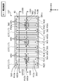
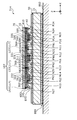
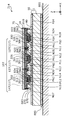
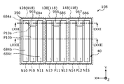
[構成]
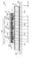
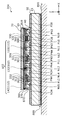
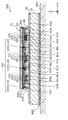
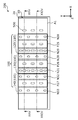
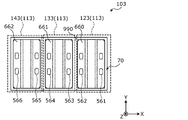
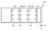
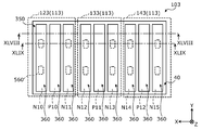
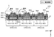
図1は、実施の形態1に係るアレー型半導体レーザ装置200を示す上面図である。図2は、図1のII-II線における、実施の形態1に係るアレー型半導体レーザ装置200を示す断面図である。図3は、実施の形態1に係る半導体レーザアレー素子100の下面図である。図4は、実施の形態1に係るサブマウント220を示す上面図である。図5は、実施の形態1に係る半導体レーザアレー素子100を示す断面図である。図6は、図5の破線VIで囲まれた領域を示す拡大図である。 (Embodiment 1)
[composition]
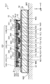
FIG. 1 is a top view showing the array typesemiconductor laser device 200 according to the first embodiment. FIG. 2 is a cross-sectional view showing the array type semiconductor laser device 200 according to the first embodiment on the line II-II of FIG. FIG. 3 is a bottom view of the semiconductor laser array element 100 according to the first embodiment. FIG. 4 is a top view showing the submount 220 according to the first embodiment. FIG. 5 is a cross-sectional view showing the semiconductor laser array element 100 according to the first embodiment. FIG. 6 is an enlarged view showing a region surrounded by the broken line VI of FIG.
[構成]
図1は、実施の形態1に係るアレー型半導体レーザ装置200を示す上面図である。図2は、図1のII-II線における、実施の形態1に係るアレー型半導体レーザ装置200を示す断面図である。図3は、実施の形態1に係る半導体レーザアレー素子100の下面図である。図4は、実施の形態1に係るサブマウント220を示す上面図である。図5は、実施の形態1に係る半導体レーザアレー素子100を示す断面図である。図6は、図5の破線VIで囲まれた領域を示す拡大図である。 (Embodiment 1)
[composition]
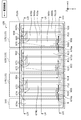
FIG. 1 is a top view showing the array type
アレー型半導体レーザ装置200は、基板10上に半導体レーザ素子120と半導体レーザ素子130と半導体レーザ素子140が互いに電気的に分離して形成されたアレー型の半導体レーザ装置である。
The array-type semiconductor laser device 200 is an array-type semiconductor laser device in which the semiconductor laser element 120, the semiconductor laser element 130, and the semiconductor laser element 140 are electrically separated from each other and formed on the substrate 10.
なお、半導体レーザ素子120と半導体レーザ素子130と半導体レーザ素子140とが互いに電気的に分離しているとは、例えば、半導体レーザ素子120と半導体レーザ素子130と半導体レーザ素子140とにおいて、各々が有する一導電型半導体層間、活性層間、及び、他導電型半導体層間が、直接接触しておらず(言い換えると、物理的に分断されており)、且つ、半導体レーザ素子120と半導体レーザ素子130と(及び半導体レーザ素子130と半導体レーザ素子140と)が、外部の配線を介して電気的に接続することを示す。例えば、半導体レーザ素子120において、一導電型半導体層300は、外部の配線を介することなく、活性層310を介して他導電型半導体層320に接続している。
The semiconductor laser element 120, the semiconductor laser element 130, and the semiconductor laser element 140 are electrically separated from each other. For example, in the semiconductor laser element 120, the semiconductor laser element 130, and the semiconductor laser element 140, each of them is said to be electrically separated from each other. The one conductive semiconductor layer, the active layer, and the other conductive semiconductor layer have no direct contact (in other words, are physically separated), and the semiconductor laser element 120 and the semiconductor laser element 130 (And the semiconductor laser element 130 and the semiconductor laser element 140) are shown to be electrically connected via an external wiring. For example, in the semiconductor laser device 120, the one conductive semiconductor layer 300 is connected to the other conductive semiconductor layer 320 via the active layer 310 without the need for external wiring.
また、半導体レーザ素子120と半導体レーザ素子130と半導体レーザ素子140とは、この順に電気的に直列に接続されている。例えば、半導体レーザ素子120における一導電型半導体層300と、半導体レーザ素子130における一導電型半導体層301とは、活性層311を介して電気的に接続されている。
Further, the semiconductor laser element 120, the semiconductor laser element 130, and the semiconductor laser element 140 are electrically connected in series in this order. For example, the monoconductive semiconductor layer 300 in the semiconductor laser element 120 and the monoconductive semiconductor layer 301 in the semiconductor laser element 130 are electrically connected via the active layer 311.
アレー型半導体レーザ装置200は、基板10と、半導体レーザアレー素子100と、基台20と、を備える。
The array type semiconductor laser device 200 includes a substrate 10, a semiconductor laser array element 100, and a base 20.
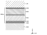
基板10は、下面に半導体レーザアレー素子100が形成される半導体基板である。基板10は、例えば、GaAs基板である。基板10には、障壁層810が形成されている。
The substrate 10 is a semiconductor substrate on which the semiconductor laser array element 100 is formed on the lower surface. The substrate 10 is, for example, a GaAs substrate. A barrier layer 810 is formed on the substrate 10.
障壁層810は、電気的絶縁性を有する層である。障壁層810は、基板10と一導電型半導体層300との間と、基板10と一導電型半導体層301と、基板10と一導電型半導体層302との間とに形成されている。障壁層810は、例えば、i-GaAs層である。障壁層810の厚さL6は、例えば、5μm以上である。
The barrier layer 810 is a layer having an electrical insulating property. The barrier layer 810 is formed between the substrate 10 and the monoconductive semiconductor layer 300, between the substrate 10 and the monoconductive semiconductor layer 301, and between the substrate 10 and the monoconductive semiconductor layer 302. The barrier layer 810 is, for example, an i-GaAs layer. The thickness L6 of the barrier layer 810 is, for example, 5 μm or more.
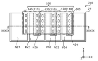
半導体レーザアレー素子100は、複数の導波路330、331、332(及び、発光点)を有し、複数のレーザ光を出力する半導体レーザ素子である。発光点は、半導体レーザアレー素子100がレーザ光を出射する位置であり、例えば、図2に示す導波路330~332の位置である。半導体レーザアレー素子100は、複数の半導体レーザ素子110を有する。本実施の形態では、半導体レーザアレー素子100は、半導体レーザ素子120(第1の半導体レーザ素子)と、半導体レーザ素子130(第2の半導体レーザ素子)と、半導体レーザ素子140(第3の半導体レーザ素子)と、を有する。半導体レーザ素子120は、n電極N10、p電極P10及びn電極N11を備える。また、半導体レーザ素子130は、n電極N12、p電極P11及びn電極N13を備える。また、半導体レーザ素子140は、n電極N14、p電極P12及びn電極N15を備える。なお、導波路330~332のX軸方向の幅は、p電極P10~P12のX軸方向の幅とほぼ等しい。
The semiconductor laser array element 100 is a semiconductor laser element having a plurality of waveguides 330, 331, 332 (and light emitting points) and outputting a plurality of laser beams. The light emitting point is a position where the semiconductor laser array element 100 emits laser light, for example, a position of the waveguides 330 to 332 shown in FIG. The semiconductor laser array element 100 has a plurality of semiconductor laser elements 110. In the present embodiment, the semiconductor laser array element 100 includes a semiconductor laser element 120 (first semiconductor laser element), a semiconductor laser element 130 (second semiconductor laser element), and a semiconductor laser element 140 (third semiconductor laser). Element) and. The semiconductor laser device 120 includes an n-electrode N10, a p-electrode P10, and an n-electrode N11. Further, the semiconductor laser element 130 includes an n electrode N12, a p electrode P11, and an n electrode N13. Further, the semiconductor laser element 140 includes an n electrode N14, a p electrode P12, and an n electrode N15. The width of the waveguides 330 to 332 in the X-axis direction is substantially equal to the width of the p-electrodes P10 to P12 in the X-axis direction.
なお、半導体レーザ素子120と、半導体レーザ素子130と、半導体レーザ素子140とで共通の説明をする場合、単に半導体レーザ素子110ともいう。
When the semiconductor laser element 120, the semiconductor laser element 130, and the semiconductor laser element 140 have a common description, they are also simply referred to as the semiconductor laser element 110.
半導体レーザアレー素子100が有する半導体レーザ素子110の数は、複数であればよく、特に限定されない。半導体レーザアレー素子100が有する複数の半導体レーザ素子110は、直列に接続されている。したがって、半導体レーザ素子120と半導体レーザ素子130とは、直列に接続されている。
The number of the semiconductor laser elements 110 included in the semiconductor laser array element 100 may be a plurality, and is not particularly limited. A plurality of semiconductor laser elements 110 included in the semiconductor laser array element 100 are connected in series. Therefore, the semiconductor laser element 120 and the semiconductor laser element 130 are connected in series.
半導体レーザ素子120は、基板10側から一導電型半導体層300(第1の一導電型半導体層)と、活性層310と、他導電型半導体層320(第1の他導電型半導体層)と、を有する。また、半導体レーザ素子120は、基板10面内の第1の方向(本実施の形態では、Y軸方向)に延びる導波路330(第1の導波路)を有する。導波路330は、例えば、一導電型半導体層300と、活性層310と、他導電型半導体層320とのそれぞれの一部で構成されるレーザ光の導波部分である。
The semiconductor laser element 120 includes a monoconductive semiconductor layer 300 (first one conductive semiconductor layer), an active layer 310, and another conductive semiconductor layer 320 (first other conductive semiconductor layer) from the substrate 10 side. Has. Further, the semiconductor laser device 120 has a waveguide 330 (first waveguide) extending in the first direction (in the present embodiment, the Y-axis direction) in the surface of the substrate 10. The waveguide 330 is, for example, a waveguide portion of laser light composed of a part of each of the one conductive semiconductor layer 300, the active layer 310, and the other conductive semiconductor layer 320.
また、半導体レーザ素子120は、p電極P10(第1電極)と、n電極N11(第3電極)と、n電極N10(第4電極)と、を有する。
Further, the semiconductor laser element 120 has a p electrode P10 (first electrode), an n electrode N11 (third electrode), and an n electrode N10 (fourth electrode).
p電極P10は、基板10と反対側に位置する面(下面又は第1面40ともいう)において、他導電型半導体層320に電気的に接続するように形成された電極である。
The p-electrode P10 is an electrode formed so as to be electrically connected to the other conductive semiconductor layer 320 on a surface (also referred to as a lower surface or a first surface 40) located on the opposite side of the substrate 10.
n電極N11は、第1面40において、一導電型半導体層300に電気的に接続するように形成され、且つ、p電極P10とp電極P11との間に配置された電極である。
The n-electrode N11 is an electrode formed on the first surface 40 so as to be electrically connected to the monoconductive semiconductor layer 300 and arranged between the p-electrode P10 and the p-electrode P11.
n電極N10は、第1面40において、一導電型半導体層300に形成され、且つ、p電極P10に対してn電極N11とは反対側に配置された電極である。言い換えると、p電極P10は、上面視でn電極N11とn電極N10の間に位置する。
The n-electrode N10 is an electrode formed on the monoconductive semiconductor layer 300 on the first surface 40 and arranged on the side opposite to the n-electrode N11 with respect to the p-electrode P10. In other words, the p-electrode P10 is located between the n-electrode N11 and the n-electrode N10 in top view.
また、図6に示すように、障壁層810とn電極N10との間における一導電型半導体層300の厚さL5は、例えば、5μm以上である。
Further, as shown in FIG. 6, the thickness L5 of the monoconductive semiconductor layer 300 between the barrier layer 810 and the n electrode N10 is, for example, 5 μm or more.
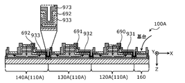
また、半導体レーザ素子120は、絶縁膜340と、保護膜350と、配線電極360と、を有する。
Further, the semiconductor laser element 120 has an insulating film 340, a protective film 350, and a wiring electrode 360.
絶縁膜340は、電気的絶縁性を有する膜である。絶縁膜340は、一導電型半導体層300、活性層310、及び、他導電型半導体層320等の半導体層の側面を覆う。絶縁膜340のX軸方向の幅L7は、例えば、15μm以上である。
The insulating film 340 is a film having electrical insulating properties. The insulating film 340 covers the side surfaces of the semiconductor layer such as the one conductive semiconductor layer 300, the active layer 310, and the other conductive semiconductor layer 320. The width L7 of the insulating film 340 in the X-axis direction is, for example, 15 μm or more.
保護膜350は、絶縁膜340を覆い、絶縁膜340及び各半導体層を保護するための膜である。
The protective film 350 is a film that covers the insulating film 340 and protects the insulating film 340 and each semiconductor layer.
配線電極360は、n電極N10、N11及びp電極P10を、基台20に形成された配線等の他の構成要素と電気的に接続するための電極である。
The wiring electrode 360 is an electrode for electrically connecting the n electrodes N10, N11 and the p electrode P10 to other components such as wiring formed on the base 20.
配線電極360の厚さL8は、例えば、3μm以上である。
The thickness L8 of the wiring electrode 360 is, for example, 3 μm or more.
なお、図6に示す半導体レーザ素子120の構成は、半導体レーザ素子130及び半導体レーザ素子140もまた同様である。
The configuration of the semiconductor laser element 120 shown in FIG. 6 is the same for the semiconductor laser element 130 and the semiconductor laser element 140.
半導体レーザ素子130は、基板10側から一導電型半導体層301(第2の一導電型半導体層)と、活性層311と、他導電型半導体層321(第2の他導電型半導体層)と、を有する。また、半導体レーザ素子130は、第1の方向に延びる導波路331(第2の導波路)を有する。
The semiconductor laser element 130 includes a monoconductive semiconductor layer 301 (second one conductive semiconductor layer), an active layer 311 and another conductive semiconductor layer 321 (second other conductive semiconductor layer) from the substrate 10 side. Has. Further, the semiconductor laser device 130 has a waveguide 331 (second waveguide) extending in the first direction.
また、半導体レーザ素子130は、p電極P11(第2電極)と、n電極N12(第5電極)と、n電極N13(第6電極)と、を有する。
Further, the semiconductor laser element 130 has a p-electrode P11 (second electrode), an n-electrode N12 (fifth electrode), and an n-electrode N13 (sixth electrode).
p電極P11は、第1面40において、他導電型半導体層321に形成された電極である。
The p-electrode P11 is an electrode formed on the other conductive semiconductor layer 321 on the first surface 40.
n電極N12は、第1面40において、一導電型半導体層301に形成され、且つ、n電極N11とp電極P11との間に配置された電極である。
The n-electrode N12 is an electrode formed on the one-conductive semiconductor layer 301 on the first surface 40 and arranged between the n-electrode N11 and the p-electrode P11.
n電極N13は、第1面40において、一導電型半導体層301に形成され、且つ、p電極P11に対してn電極N12とは反対側に配置された電極である。
The n-electrode N13 is an electrode formed on the monoconductive semiconductor layer 301 on the first surface 40 and arranged on the side opposite to the n-electrode N12 with respect to the p-electrode P11.
半導体レーザ素子140は、基板10側から一導電型半導体層302(第3の一導電型半導体層)と、活性層312と、他導電型半導体層322(第3の他導電型半導体層)と、を有する。また、半導体レーザ素子140は、第1の方向に延びる導波路332(第3の導波路)を有する。
The semiconductor laser element 140 includes a monoconductive semiconductor layer 302 (third one conductive semiconductor layer), an active layer 312, and another conductive semiconductor layer 322 (third other conductive semiconductor layer) from the substrate 10 side. Has. Further, the semiconductor laser device 140 has a waveguide 332 (third waveguide) extending in the first direction.
また、半導体レーザ素子140は、p電極P12と、n電極N14と、n電極N15と、を有する。
Further, the semiconductor laser element 140 has a p-electrode P12, an n-electrode N14, and an n-electrode N15.
p電極P12は、第1面40において、他導電型半導体層322に形成された電極である。
The p-electrode P12 is an electrode formed on the other conductive semiconductor layer 322 on the first surface 40.
n電極N14及びn電極N15は、第1面40において、一導電型半導体層302に形成される。
The n-electrode N14 and the n-electrode N15 are formed on the monoconductive semiconductor layer 302 on the first surface 40.
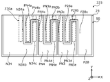
また、図3に示すように、半導体レーザ素子130は、半導体レーザ素子120に対して、第1の方向と直交する基板10面内の第2の方向(本実施の形態では、X軸方向)において、並んで配置されている。上面視で、n電極N15、p電極P12、n電極N14、n電極N13、p電極P11、n電極N12、n電極N11、p電極P10、及び、n電極N10は、各々矩形であり、この順にX軸方向に平行に並んで配置される。なお、図3において、半導体レーザアレー素子100を下面から見て、n電極N15、p電極P12、n電極N14、n電極N13、p電極P11、n電極N12、n電極N11、p電極P10、及び、n電極N10は、それぞれの配線電極360とほぼ同じ形状の矩形で形成され、それぞれの配線電極360に覆われている。また、半導体レーザアレー素子100の下面の配線電極360が露出していない部分は、保護膜350で覆われている。
Further, as shown in FIG. 3, the semiconductor laser element 130 has a second direction in the surface of the substrate 10 orthogonal to the first direction with respect to the semiconductor laser element 120 (in the present embodiment, the X-axis direction). In, they are arranged side by side. In top view, the n-electrode N15, p-electrode P12, n-electrode N14, n-electrode N13, p-electrode P11, n-electrode N12, n-electrode N11, p-electrode P10, and n-electrode N10 are each rectangular, in that order. They are arranged side by side in parallel in the X-axis direction. In FIG. 3, when the semiconductor laser array element 100 is viewed from the lower surface, the n electrode N15, the p electrode P12, the n electrode N14, the n electrode N13, the p electrode P11, the n electrode N12, the n electrode N11, the p electrode P10, and the like. The n-electrode N10 is formed of a rectangle having substantially the same shape as each of the wiring electrodes 360, and is covered with each of the wiring electrodes 360. Further, the portion where the wiring electrode 360 on the lower surface of the semiconductor laser array element 100 is not exposed is covered with the protective film 350.
また、例えば、半導体レーザ素子120及び半導体レーザ素子130の少なくとも一方は、横多モードで発振する。例えば、半導体レーザ素子120及び半導体レーザ素子130の少なくとも一方は、横多モードで発振するように、導波路330、331の幅が調整されている。
Further, for example, at least one of the semiconductor laser element 120 and the semiconductor laser element 130 oscillates in the horizontal multi-mode. For example, the widths of the waveguides 330 and 331 are adjusted so that at least one of the semiconductor laser element 120 and the semiconductor laser element 130 oscillates in the horizontal multimode.
また、一導電型半導体層300と一導電型半導体層301とは、それぞれn型半導体層を含む。また、他導電型半導体層320と他導電型半導体層321とは、それぞれp型半導体層を含む。
Further, the monoconductive semiconductor layer 300 and the monoconductive semiconductor layer 301 each include an n-type semiconductor layer. Further, the other conductive type semiconductor layer 320 and the other conductive type semiconductor layer 321 each include a p-type semiconductor layer.
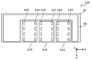
サブマウント220は、基台20にパターン配線が形成されたものである。基台20(第1の基台)は、上面(第2面50)に半導体レーザアレー素子100が配置(実装)される基板である。本実施の形態では、基台20には、半導体レーザアレー素子100がフリップチップ実装されている。
The sub mount 220 has a pattern wiring formed on the base 20. The base 20 (first base) is a substrate on which the semiconductor laser array element 100 is arranged (mounted) on the upper surface (second surface 50). In the present embodiment, the semiconductor laser array element 100 is flip-chip mounted on the base 20.
図4に示すように、第2面50には、パターン配線として、p側の導電膜である上面視で矩形のp配線P20、P21、P22、P23、及び、n側の導電膜である上面視でU字状のn配線N20、N21、N22が形成されている。ここで、p配線P21は、n配線N20の一端の直線部分N20aと他端の直線部分N20bとに挟まれている。同様に、p配線P22は、n配線N21の一端の直線部分N21aと他端の直線部分N21bとに挟まれている。また、同様に、p配線P23は、n配線N22の一端の直線部分N22aと他端の直線部分N22bとに挟まれている。直線部分N22a、p配線P23、直線部分N22b、直線部分N21a、p配線P22、直線部分N21b、直線部分N20a、p配線P21、直線部分N20b、及び、p配線P20は、この順にX軸方向に平行に並んで配置される。
As shown in FIG. 4, on the second surface 50, as the pattern wiring, the p-wirings P20, P21, P22, P23, which are rectangular p-wiring in the top view, which is the conductive film on the p-side, and the upper surface, which is the conductive film on the n-side. Visually, U-shaped n wirings N20, N21, and N22 are formed. Here, the p-wiring P21 is sandwiched between a straight portion N20a at one end and a straight portion N20b at the other end of the n-wiring N20. Similarly, the p-wiring P22 is sandwiched between a straight portion N21a at one end and a straight portion N21b at the other end of the n-wiring N21. Similarly, the p-wiring P23 is sandwiched between a straight portion N22a at one end and a straight portion N22b at the other end of the n-wiring N22. The straight portion N22a, the p wiring P23, the straight portion N22b, the straight portion N21a, the p wiring P22, the straight portion N21b, the straight portion N20a, the p wiring P21, the straight portion N20b, and the p wiring P20 are parallel in the X-axis direction in this order. Arranged side by side.
半導体レーザアレー素子100が有するp電極及びn電極は、配線電極360と接続層370を介して、基台20に形成されているパターン配線と電気的に接続されている。
The p-electrode and n-electrode of the semiconductor laser array element 100 are electrically connected to the pattern wiring formed on the base 20 via the wiring electrode 360 and the connection layer 370.
例えば、n電極N10とn電極N11とは、配線電極360と接続層370を介してn配線N20の直線部分N20bと直線部分N20aに、それぞれ、電気的に接続されている。また、例えば、n電極N12とn電極N13とは、配線電極360と接続層370を介してn配線N21の直線部分N21bと直線部分N21aに、それぞれ、電気的に接続されている。また、例えば、n電極N14とn電極N15とは、配線電極360と接続層370を介してn配線N22の直線部分N22bと直線部分N22aに、それぞれ、電気的に接続されている。また、例えば、p電極P10は、配線電極360と接続層370を介してp配線P21と電気的に接続されている。また、例えば、p電極P11は、配線電極360と接続層370を介してp配線P22と電気的に接続されている。また、例えば、p電極P12は、配線電極360と接続層370を介してp配線P23と電気的に接続されている。
For example, the n-electrode N10 and the n-electrode N11 are electrically connected to the straight portion N20b and the straight portion N20a of the n wiring N20 via the wiring electrode 360 and the connection layer 370, respectively. Further, for example, the n-electrode N12 and the n-electrode N13 are electrically connected to the straight portion N21b and the straight portion N21a of the n-wiring N21 via the wiring electrode 360 and the connection layer 370, respectively. Further, for example, the n-electrode N14 and the n-electrode N15 are electrically connected to the straight portion N22b and the straight portion N22a of the n-wiring N22 via the wiring electrode 360 and the connection layer 370, respectively. Further, for example, the p-electrode P10 is electrically connected to the p-wiring P21 via the wiring electrode 360 and the connection layer 370. Further, for example, the p-electrode P11 is electrically connected to the p-wiring P22 via the wiring electrode 360 and the connection layer 370. Further, for example, the p-electrode P12 is electrically connected to the p-wiring P23 via the wiring electrode 360 and the connection layer 370.
また、n配線N20の中央部N20c、n配線N21の中央部N21c、n配線N22の中央部N22c、p配線P21の一端P21a、p配線P22の一端P22a、及び、p配線P23の一端P23aは、Y軸方向において、半導体レーザ素子120及び半導体レーザ素子130それぞれの後端(本実施の形態では、Y軸負方向側の端部)から露出している。第1導電膜(第1導電体)と第2導電膜(第2導電体)とは、第1の方向において、半導体レーザ素子120の後端から露出している。第2導電膜は、半導体レーザ素子120から露出し、且つ、n電極N12と電気的に接続する第3部分730と、半導体レーザ素子120から露出し、且つ、n電極N13と電気的に接続する第4部分740とを有する。
Further, the central portion N20c of the n-wiring N20, the central portion N21c of the n-wiring N21, the central portion N22c of the n-wiring N22, one end P21a of the p-wiring P21, one end P22a of the p-wiring P22, and one end P23a of the p-wiring P23 are In the Y-axis direction, the semiconductor laser element 120 and the semiconductor laser element 130 are exposed from the rear ends (in the present embodiment, the end on the negative direction side of the Y-axis). The first conductive film (first conductor) and the second conductive film (second conductor) are exposed from the rear end of the semiconductor laser device 120 in the first direction. The second conductive film is exposed from the semiconductor laser element 120 and electrically connected to the n electrode N12 and the third portion 730, and is exposed from the semiconductor laser element 120 and electrically connected to the n electrode N13. It has a fourth portion 740 and.
第2面50上には、各パターン配線を電気的に接続するための金属製のワイヤW1~W3が形成されている。例えば、p配線P20とp配線P21とは、p配線P20と一端P21aとに接合されたワイヤW1により電気的に接続されている。また、例えば、n配線N20とp配線P22とは、中央部N20cと一端P22aとに接合されたワイヤW2により電気的に接続されている。また、例えば、n配線N21とp配線P23とは、中央部N21cと一端P23aとに接合されたワイヤW3により電気的に接続されている。ワイヤW1、W2、W3の各々は、4本のAu線からなる。
Metal wires W1 to W3 for electrically connecting each pattern wiring are formed on the second surface 50. For example, the p-wiring P20 and the p-wiring P21 are electrically connected by a wire W1 joined to the p-wiring P20 and one end P21a. Further, for example, the n-wiring N20 and the p-wiring P22 are electrically connected by a wire W2 joined to the central portion N20c and one end P22a. Further, for example, the n-wiring N21 and the p-wiring P23 are electrically connected by a wire W3 joined to the central portion N21c and one end P23a. Each of the wires W1, W2, and W3 consists of four Au wires.
p電極P11とn電極N11とは、n配線N20、ワイヤW2、及び、p配線P22を介して、電気的に接続されている。本実施の形態では、n配線N20、ワイヤW2、及び、p配線P22が、第1導電体である。
The p-electrode P11 and the n-electrode N11 are electrically connected via the n-wiring N20, the wire W2, and the p-wiring P22. In the present embodiment, the n-wiring N20, the wire W2, and the p-wiring P22 are the first conductors.
また、n電極N12とn電極N13とは、n配線N21を介して電気的に接続されている。つまり、本実施の形態では、導電膜(第2導電膜)であるn配線N21が、第2導電体である。同様に、n電極N10とn電極N11とは、n配線N20を介して電気的に接続され、n電極N14とn電極N15とは、n配線N22を介して電気的に接続されている。
Further, the n-electrode N12 and the n-electrode N13 are electrically connected via the n-wiring N21. That is, in the present embodiment, the n wiring N21 which is a conductive film (second conductive film) is the second conductor. Similarly, the n-electrode N10 and the n-electrode N11 are electrically connected via the n-wiring N20, and the n-electrode N14 and the n-electrode N15 are electrically connected via the n-wiring N22.
n配線N21における、X軸方向に延在している箇所における、当該箇所の幅(Y軸方向の長さL3)は、例えば、60μm以下である。また、n配線N21における、X軸方向に延在している箇所における、当該延在方向(つまり、X軸方向)の長さL4(ブリッジ配線長さ)は、例えば、630μm程度である。
The width of the portion of the n wiring N21 extending in the X-axis direction (length L3 in the Y-axis direction) is, for example, 60 μm or less. Further, the length L4 (bridge wiring length) in the extending direction (that is, the X-axis direction) at the portion extending in the X-axis direction in the n wiring N21 is, for example, about 630 μm.
アレー型半導体レーザ装置200は、第1の金属線(ワイヤW2)を備える。第1の金属線(ワイヤW2)は、p配線P22の第1部分710とn配線N20の第2部分720とを電気的に接続する金属線である。p配線P22の第1部分710は、上記したp配線P22の一端P22aと同じ領域を指す。
The array type semiconductor laser device 200 includes a first metal wire (wire W2). The first metal wire (wire W2) is a metal wire that electrically connects the first portion 710 of the p-wiring P22 and the second portion 720 of the n-wiring N20. The first portion 710 of the p-wiring P22 points to the same region as one end P22a of the p-wiring P22 described above.
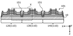
また、アレー型半導体レーザ装置200は、半導体レーザ素子120と半導体レーザ素子130との間に、凹部150を有する。本実施の形態では、半導体レーザアレー素子100に、凹部150が形成されている。
Further, the array type semiconductor laser device 200 has a recess 150 between the semiconductor laser element 120 and the semiconductor laser element 130. In the present embodiment, the recess 150 is formed in the semiconductor laser array element 100.
凹部150は、半導体レーザ素子120と半導体レーザ素子130との間に形成され、半導体レーザ素子120と半導体レーザ素子130とが配線等を介さずに電気的に接続されることを防ぐための溝である。凹部150は、障壁層810に達する溝である。例えば、障壁層810にも凹部150の一部が形成されている。凹部150には、絶縁膜340及び保護膜350が形成されている。
The recess 150 is formed between the semiconductor laser element 120 and the semiconductor laser element 130, and is a groove for preventing the semiconductor laser element 120 and the semiconductor laser element 130 from being electrically connected without wiring or the like. be. The recess 150 is a groove that reaches the barrier layer 810. For example, a part of the recess 150 is also formed in the barrier layer 810. An insulating film 340 and a protective film 350 are formed in the recess 150.
基台20には、半導体レーザアレー素子100が実装される。基台20は、例えば、絶縁性を有する。
The semiconductor laser array element 100 is mounted on the base 20. The base 20 has, for example, insulating properties.
本実施の形態では、基板10の第1面40(下面)側が、基台20の第2面50(上面)に接合されている。
In the present embodiment, the first surface 40 (lower surface) side of the substrate 10 is joined to the second surface 50 (upper surface) of the base 20.
例えば、上面視した場合に、半導体レーザアレー素子100と重ならない箇所におけるp配線P21、P22、P23のそれぞれのY軸方向の長さL2は、500μm以下である。
For example, when viewed from above, the length L2 of each of the p wirings P21, P22, and P23 in the Y-axis direction at a location that does not overlap with the semiconductor laser array element 100 is 500 μm or less.
半導体レーザアレー素子100と基台20とは、接続部870により接続されている。
The semiconductor laser array element 100 and the base 20 are connected by a connecting portion 870.
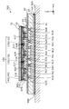
図7は、実施の形態1に係る接続部870を示す断面図である。
FIG. 7 is a cross-sectional view showing a connection portion 870 according to the first embodiment.
接続部870において、配線電極360は、上層側から順に、例えば、金属層871と、バリアメタル層872とで構成されている。また、接続層370は、半田層873と、半田用下地層874とで構成されている。また、パターン配線(例としては、n配線N22)は、上面導電層875と、下地層876と、有する。下地層876は、基台20上に形成されている。図4に示すように、パターン配線上の点線で示す接続領域370aに接続層370が形成される。
In the connection portion 870, the wiring electrode 360 is composed of, for example, a metal layer 871 and a barrier metal layer 872 in order from the upper layer side. Further, the connection layer 370 is composed of a solder layer 873 and a solder base layer 874. Further, the pattern wiring (for example, n wiring N22) has an upper surface conductive layer 875 and a base layer 876. The base layer 876 is formed on the base 20. As shown in FIG. 4, the connection layer 370 is formed in the connection region 370a shown by the dotted line on the pattern wiring.
金属層871は、例えば、Auからなる。金属層871は、例えば、メッキで形成される。
The metal layer 871 is made of, for example, Au. The metal layer 871 is formed by plating, for example.
バリアメタル層872は、例えば、下層側から順にPt層と、Ti層とからなる。
The barrier metal layer 872 is composed of, for example, a Pt layer and a Ti layer in order from the lower layer side.
半田層873は、例えば、AuSn半田からなる。
The solder layer 873 is made of, for example, AuSn solder.
半田用下地層874は、例えば、下層側から順に、Ti層と、Pt層とからなる。
The solder base layer 874 is composed of, for example, a Ti layer and a Pt layer in order from the lower layer side.
上面導電層875は、例えば、下層側から順に、Cu層と、Ni層と、Au層とからなる。上面導電層875は、例えば、メッキで形成される。
The upper surface conductive layer 875 is composed of, for example, a Cu layer, a Ni layer, and an Au layer in order from the lower layer side. The upper surface conductive layer 875 is formed by plating, for example.
下地層876は、例えば、下層側から順に、Ti層と、Pt層と、Au層とからなり、上面導電層875をメッキで形成する場合の下地となる層である。
The base layer 876 is composed of, for example, a Ti layer, a Pt layer, and an Au layer in this order from the lower layer side, and is a layer that serves as a base when the upper surface conductive layer 875 is formed by plating.
基台20は、例えば、AlN、SiC等の絶縁性セラミック材料からなる。
The base 20 is made of, for example, an insulating ceramic material such as AlN or SiC.
また、アレー型半導体レーザ装置200は、さらに、第1の端子と、第2の端子とを備える。
Further, the array type semiconductor laser device 200 further includes a first terminal and a second terminal.
第1の端子は、p電極P10と電気的に接続される端子である。本実施の形態では、第1の端子は、基台20に形成された配線であるp配線P20である。
The first terminal is a terminal that is electrically connected to the p electrode P10. In the present embodiment, the first terminal is the p-wiring P20, which is the wiring formed on the base 20.
第2の端子は、n電極N12と電気的に接続される端子である。本実施の形態では、第2の端子は、基台20に形成された配線であるn配線N22である。なお、本実施の形態では、n電極N12は、n配線N21、ワイヤW3、p配線P23、及び、半導体レーザ素子140を介してn配線N22と電気的に接続されている。
The second terminal is a terminal that is electrically connected to the n electrode N12. In the present embodiment, the second terminal is the n-wiring N22, which is the wiring formed on the base 20. In the present embodiment, the n-electrode N12 is electrically connected to the n-wiring N22 via the n-wiring N21, the wire W3, the p-wiring P23, and the semiconductor laser element 140.
半導体レーザアレー素子100には、図示しない外部電源等から、第1の端子及び第2の端子を介して、直流電流が印加される。
A direct current is applied to the semiconductor laser array element 100 from an external power source (not shown) or the like via the first terminal and the second terminal.
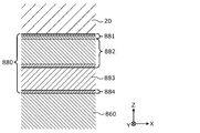
基台20は、接合層880を介してヒートシンク860に載置されている。
The base 20 is placed on the heat sink 860 via the bonding layer 880.
ヒートシンク860は、例えば、Cu、Al等の熱伝導性の高い金属材料から形成される。
The heat sink 860 is formed of, for example, a metal material having high thermal conductivity such as Cu and Al.
ヒートシンク860と基台20とは、例えば、SnAgCu等の半田で接合されている。
The heat sink 860 and the base 20 are joined by solder such as SnAgCu.
図8は、実施の形態1に係る接合層880を示す断面図である。
FIG. 8 is a cross-sectional view showing the bonding layer 880 according to the first embodiment.
接合層880は、上層側から順に、下地層881と、下面導電層882と、半田層883と、上面導電層884と、を有する。
The bonding layer 880 has a base layer 881, a lower surface conductive layer 882, a solder layer 883, and an upper surface conductive layer 884 in this order from the upper layer side.
下地層881は、例えば、下層側から順に、Au層と、Pt層と、Ti層とからなる。
The base layer 881 is composed of, for example, an Au layer, a Pt layer, and a Ti layer in order from the lower layer side.
下面導電層882は、例えば、下層側から順に、Au層と、Ni層と、Cu層とからなる。下面導電層882は、例えばメッキで形成される層であり、この場合、下地層881は、下面導電層882の下地となる層である。
The lower surface conductive layer 882 is composed of, for example, an Au layer, a Ni layer, and a Cu layer in order from the lower layer side. The lower surface conductive layer 882 is a layer formed by plating, for example, and in this case, the base layer 881 is a layer that serves as a base for the lower surface conductive layer 882.
半田層883は、例えば、SnAgCu系低融点半田からなる。
The solder layer 883 is made of, for example, SnAgCu-based low melting point solder.
上面導電層884は、例えば、下層側から順に、Ni層と、Au層とからなる。上面導電層884は、例えば、メッキで形成される層である。
The upper surface conductive layer 884 is composed of, for example, a Ni layer and an Au layer in order from the lower layer side. The upper surface conductive layer 884 is, for example, a layer formed by plating.
以上のような構成によれば、アレー型半導体レーザ装置200には、半導体レーザ素子110間、及び、半導体レーザ素子110と基台20とを電気的に接続する配線(跨ぎ配線又はブリッジ配線ともいう)がないので、アレー型半導体レーザ装置200の製造プロセスがより容易に設計できるメリットがある。また、基台20に関しても、特別なプロセスが不要であり、容易に設計可能である。また、アレー型半導体レーザ装置200を製造する際の組立工程としても、注意点(リスク)が少なく、実現度が高い構成である。
According to the above configuration, in the array type semiconductor laser device 200, wiring (also referred to as straddle wiring or bridge wiring) for electrically connecting the semiconductor laser element 110 and the semiconductor laser element 110 and the base 20 is provided. ), Therefore, there is an advantage that the manufacturing process of the array type semiconductor laser device 200 can be designed more easily. Further, the base 20 does not require a special process and can be easily designed. Further, as an assembly process when manufacturing the array type semiconductor laser device 200, there are few precautions (risks) and the configuration is highly feasible.
アレー型半導体レーザ装置200における電気の流れとしては、アノード電極であるp配線P20を開始として、p配線P20→ワイヤW1→p配線P21→p電極P10→n電極N10、N11→n配線N20→ワイヤW2→p配線P22→p電極P11→n電極N12、N13→n配線N21→ワイヤW3→p配線P23→p電極P12→n電極N14、N15→カソード電極であるn配線N22となる。
As the flow of electricity in the array type semiconductor laser apparatus 200, starting from the p-wire P20 which is the anode electrode, the p-wire P20 → wire W1 → p-wire P21 → p-electrode P10 → n-electrode N10, N11 → n-wire N20 → wire W2 → p wiring P22 → p electrode P11 → n electrode N12, N13 → n wiring N21 → wire W3 → p wiring P23 → p electrode P12 → n electrode N14, N15 → n wiring N22 which is a cathode electrode.
複数の半導体レーザ素子110それぞれの共振器長(Y軸方向の長さ、より具体的には、長さL1)は、例えば、4mmである。
The resonator length (length in the Y-axis direction, more specifically, length L1) of each of the plurality of semiconductor laser elements 110 is, for example, 4 mm.
また、基台20に形成された各配線(Cuメッキ成形)のメッキ厚は、例えば、最大で75μmであり、接続層370(厚さ5μm以上)と合わせると、80μm以上の厚さになる。隣接する各配線間の距離は、最小でメッキ厚さ×150%となっている。基台20に用いられる金属材料は、例えば、Cu、Au、Al等である。
Further, the plating thickness of each wiring (Cu plating molding) formed on the base 20 is, for example, 75 μm at the maximum, and when combined with the connection layer 370 (thickness 5 μm or more), the thickness becomes 80 μm or more. The minimum distance between adjacent wirings is the plating thickness x 150%. The metal material used for the base 20 is, for example, Cu, Au, Al, or the like.
電気配線(基台20に形成された配線及びワイヤW1、W2、W3)は、電気配線の断面積と長さで決まる抵抗値を有する。この抵抗成分は、発熱源となり、過電流が流れる等して配線材料の融点を超えると、溶け配線が断裂する。本願発明者らは、検討した結果、径が25μm、Auワイヤ(長さ:3mm)1本に、1.4Aの電流を流した場合に、ワイヤが溶断した。そこで、電気配線の構成(材料、配線長さ、及び、配線断面積)から算出される溶断電流の1/3程度の値に定格電流とする。
The electrical wiring (wiring and wires W1, W2, W3 formed on the base 20) has a resistance value determined by the cross-sectional area and length of the electrical wiring. This resistance component serves as a heat generating source, and when the melting point of the wiring material is exceeded due to an overcurrent flowing or the like, the melted wiring is torn. As a result of examination, the inventors of the present application melted the wire when a current of 1.4 A was passed through one Au wire (length: 3 mm) having a diameter of 25 μm. Therefore, the rated current is set to a value of about 1/3 of the fusing current calculated from the configuration of the electrical wiring (material, wiring length, and wiring cross-sectional area).
電気配線の材料電気伝導度をAm(%)とし、電気配線の長さをL(m)とし、電気配線の断面積をS(μm2)とした場合、以下の式(1)を満たす。
Material of electrical wiring When the electrical conductivity is Am (%), the length of the electrical wiring is L (m), and the cross-sectional area of the electrical wiring is S (μm 2 ), the following equation (1) is satisfied.
(定格電流)=(8.56×10⁻³×Am×S)/(3×L) (A) 式(1)
(Rated current) = (8.56 × 10 -3 × Am × S) / (3 × L) (A) Equation (1)
材料の電気伝導度は、Auを100%とした場合、例えば、Cuが138%であり、Alが84%であり、n-GaAsが1%である。
When Au is 100%, the electrical conductivity of the material is, for example, 138% for Cu, 84% for Al, and 1% for n-GaAs.
上記式(1)を用いて電気配線のサイズ等を決定することで、電気配線の溶断の発生を抑制することができる。
By determining the size of the electrical wiring using the above formula (1), it is possible to suppress the occurrence of fusing of the electrical wiring.
[効果等]
以上説明したように、実施の形態1に係るアレー型半導体レーザ装置200は、基板10に半導体レーザ素子120と半導体レーザ素子130とが形成された半導体レーザアレー素子100を備えるアレー型半導体レーザ装置である。半導体レーザ素子120は、基板10側から一導電型半導体層300と、他導電型半導体層320とを有しする。半導体レーザ素子130は、基板10側から一導電型半導体層301と、他導電型半導体層321とを有する。半導体レーザ素子120は、基板10面内の第1の方向(Y軸方向)に延びる導波路330を有する。半導体レーザ素子130は、半導体レーザ素子120に対して、Y軸方向と直交する基板10面内の第2の方向(X軸方向)において配置されている。半導体レーザ素子130は、Y軸方向に延びる導波路331を有する。基板10と反対側の第1面40において、半導体レーザ素子120は、他導電型半導体層320に形成された第1電極(p電極P10)を有する。第1面40において、半導体レーザ素子130は、他導電型半導体層321に形成された第2電極(p電極P11)を有する。第1面40において、半導体レーザ素子120は、一導電型半導体層300に形成され、且つ、p電極P10とp電極P11との間に配置された第3電極(n電極N11)と、一導電型半導体層300に形成され、且つ、n電極N11とp電極P10を挟んで反対側に配置された第4電極(n電極N10)とを有する。第1面40において、半導体レーザ素子130は、一導電型半導体層301に形成され、且つ、n電極N11とp電極P11との間に配置された第5電極(n電極N12)と、一導電型半導体層301に形成され、且つ、n電極N12とp電極P11を挟んで反対側に配置された第6電極(n電極N13)とを有する。アレー型半導体レーザ装置200は、p電極P11とn電極N11とを電気的に接続する第1導電体と、n電極N12とn電極N13とを電気的に接続する第2導電体とを有する。 [Effects, etc.]
As described above, the array-typesemiconductor laser device 200 according to the first embodiment is an array-type semiconductor laser device including a semiconductor laser array element 100 in which a semiconductor laser element 120 and a semiconductor laser element 130 are formed on a substrate 10. .. The semiconductor laser element 120 has one conductive semiconductor layer 300 and another conductive semiconductor layer 320 from the substrate 10 side. The semiconductor laser element 130 has one conductive semiconductor layer 301 and another conductive semiconductor layer 321 from the substrate 10 side. The semiconductor laser device 120 has a waveguide 330 extending in the first direction (Y-axis direction) in the 10 planes of the substrate. The semiconductor laser element 130 is arranged in a second direction (X-axis direction) in the surface of the substrate 10 orthogonal to the Y-axis direction with respect to the semiconductor laser element 120. The semiconductor laser device 130 has a waveguide 331 extending in the Y-axis direction. On the first surface 40 opposite to the substrate 10, the semiconductor laser element 120 has a first electrode (p electrode P10) formed on the other conductive semiconductor layer 320. On the first surface 40, the semiconductor laser element 130 has a second electrode (p electrode P11) formed on the other conductive semiconductor layer 321. On the first surface 40, the semiconductor laser element 120 has a third electrode (n electrode N11) formed on the one-conductive semiconductor layer 300 and arranged between the p-electrode P10 and the p-electrode P11, and one-conductivity. It has a fourth electrode (n electrode N10) formed on the type semiconductor layer 300 and arranged on opposite sides of the n electrode N11 and the p electrode P10. On the first surface 40, the semiconductor laser element 130 is formed on the monoconductive semiconductor layer 301, and is monoconductive with the fifth electrode (n electrode N12) arranged between the n electrode N11 and the p electrode P11. It has a sixth electrode (n electrode N13) formed on the type semiconductor layer 301 and arranged on opposite sides of the n electrode N12 and the p electrode P11. The array type semiconductor laser device 200 has a first conductor that electrically connects the p electrode P11 and the n electrode N11, and a second conductor that electrically connects the n electrode N12 and the n electrode N13.
以上説明したように、実施の形態1に係るアレー型半導体レーザ装置200は、基板10に半導体レーザ素子120と半導体レーザ素子130とが形成された半導体レーザアレー素子100を備えるアレー型半導体レーザ装置である。半導体レーザ素子120は、基板10側から一導電型半導体層300と、他導電型半導体層320とを有しする。半導体レーザ素子130は、基板10側から一導電型半導体層301と、他導電型半導体層321とを有する。半導体レーザ素子120は、基板10面内の第1の方向(Y軸方向)に延びる導波路330を有する。半導体レーザ素子130は、半導体レーザ素子120に対して、Y軸方向と直交する基板10面内の第2の方向(X軸方向)において配置されている。半導体レーザ素子130は、Y軸方向に延びる導波路331を有する。基板10と反対側の第1面40において、半導体レーザ素子120は、他導電型半導体層320に形成された第1電極(p電極P10)を有する。第1面40において、半導体レーザ素子130は、他導電型半導体層321に形成された第2電極(p電極P11)を有する。第1面40において、半導体レーザ素子120は、一導電型半導体層300に形成され、且つ、p電極P10とp電極P11との間に配置された第3電極(n電極N11)と、一導電型半導体層300に形成され、且つ、n電極N11とp電極P10を挟んで反対側に配置された第4電極(n電極N10)とを有する。第1面40において、半導体レーザ素子130は、一導電型半導体層301に形成され、且つ、n電極N11とp電極P11との間に配置された第5電極(n電極N12)と、一導電型半導体層301に形成され、且つ、n電極N12とp電極P11を挟んで反対側に配置された第6電極(n電極N13)とを有する。アレー型半導体レーザ装置200は、p電極P11とn電極N11とを電気的に接続する第1導電体と、n電極N12とn電極N13とを電気的に接続する第2導電体とを有する。 [Effects, etc.]
As described above, the array-type
なお、本実施の形態では、第1導電体は、p配線P22、n配線N20、及び、ワイヤW2である。また、本実施の形態では、第2導電体は、n配線N21である。
In the present embodiment, the first conductors are the p-wiring P22, the n-wiring N20, and the wire W2. Further, in the present embodiment, the second conductor is n wiring N21.
これによれば、半導体レーザ素子110の両側側方にn電極が配置される。これにより、導波路330、331(より具体的には、活性層310、311)には、上面視で導波路330、331の延在方向に直交する方向(X軸方向)において、中央に電流が流れやすくなる。そのため、アレー型半導体レーザ装置200によれば、複数の半導体レーザ素子110を直列接続し、且つ、活性層に流れる電流の偏りが抑制される。
According to this, n electrodes are arranged on both sides of the semiconductor laser element 110. As a result, the waveguides 330 and 331 (more specifically, the active layers 310 and 311) have a current in the center in the direction (X-axis direction) orthogonal to the extending direction of the waveguides 330 and 331 in a top view. Becomes easier to flow. Therefore, according to the array type semiconductor laser apparatus 200, a plurality of semiconductor laser elements 110 are connected in series, and the bias of the current flowing through the active layer is suppressed.
また、例えば、半導体レーザ素子120及び半導体レーザ素子130の少なくとも一方は、横多モードで発振する。
Further, for example, at least one of the semiconductor laser element 120 and the semiconductor laser element 130 oscillates in the horizontal multi-mode.
これによれば、例えば、横多モード発振となるように導波路の幅を広くすることで、アレー型半導体レーザ装置200からのレーザ光の出力を高くできる。
According to this, for example, by widening the width of the waveguide so as to cause horizontal multi-mode oscillation, the output of the laser light from the array type semiconductor laser device 200 can be increased.
また、例えば、一導電型半導体層300と一導電型半導体層301とは、n型半導体層を含み、他導電型半導体層320と他導電型半導体層321とは、p型半導体層を含む。
Further, for example, the one-conducting semiconductor layer 300 and the one-conducting semiconductor layer 301 include an n-type semiconductor layer, and the other conductive semiconductor layer 320 and the other conductive semiconductor layer 321 include a p-type semiconductor layer.
これによれば、n型半導体の方が、p型半導体より、導電率を高くできる。一導電型半導体層300と一導電型半導体層301とには、電流が層の面内方向に流れる。一導電型半導体層300と一導電型半導体層301とを両方ともn型半導体とすることで、当該層の抵抗と素子の抵抗とを下げることができるため、活性層310、311内の横方向に電流を均一に流すこと容易になる。
According to this, the conductivity of n-type semiconductors can be higher than that of p-type semiconductors. A current flows in the in-plane direction of the one-conductive semiconductor layer 300 and the one-conductive semiconductor layer 301. By using both the one-conductive semiconductor layer 300 and the one-conductive semiconductor layer 301 as n-type semiconductors, the resistance of the layer and the resistance of the element can be reduced, so that the resistance in the active layers 310 and 311 can be reduced in the lateral direction. It becomes easy to apply a uniform current to the current.
また、例えば、基板10は、絶縁性を有する。
Further, for example, the substrate 10 has an insulating property.
これによれば、半導体レーザ素子120と半導体レーザ素子130との電気的分離(絶縁)が容易に可能になる。この場合、基板10として、半絶縁性GaAs基板又は半絶縁性InP基板を用い、障壁層810を形成しなくてもよい。
According to this, the semiconductor laser element 120 and the semiconductor laser element 130 can be easily electrically separated (insulated). In this case, a semi-insulating GaAs substrate or a semi-insulating InP substrate may be used as the substrate 10, and the barrier layer 810 may not be formed.
例えば、アレー型半導体レーザ装置200は、さらに、基板10と一導電型半導体層300との間と、基板10と一導電型半導体層301との間に、それぞれ障壁層810を有する。
For example, the array type semiconductor laser device 200 further has a barrier layer 810 between the substrate 10 and the monoconductive semiconductor layer 300 and between the substrate 10 and the monoconductive semiconductor layer 301, respectively.
これによれば、基板10が、例えば、窒化物半導体等の絶縁性が得られにくい導電性を有する場合であっても、半導体レーザ素子120と半導体レーザ素子130との電気的分離が可能になる。また、基板10が絶縁性の場合であっても、半導体レーザ素子120と半導体レーザ素子130との電気的分離が、より確実になる。
According to this, even when the substrate 10 has conductivity such as a nitride semiconductor in which insulation is difficult to obtain, the semiconductor laser element 120 and the semiconductor laser element 130 can be electrically separated from each other. .. Further, even when the substrate 10 is insulating, the electrical separation between the semiconductor laser element 120 and the semiconductor laser element 130 becomes more reliable.
また、例えば、アレー型半導体レーザ装置200は、さらに、半導体レーザ素子120と半導体レーザ素子130との間に、凹部150を有する。
Further, for example, the array type semiconductor laser device 200 further has a recess 150 between the semiconductor laser element 120 and the semiconductor laser element 130.
これによれば、一導電型半導体層300と一導電型半導体層301との間の絶縁が容易に実現できるので、半導体レーザ素子120と半導体レーザ素子130との電極等を介さない位置における電気的分離が可能になる。
According to this, since the insulation between the one-conductive semiconductor layer 300 and the one-conductive semiconductor layer 301 can be easily realized, the semiconductor laser element 120 and the semiconductor laser element 130 are electrically connected at a position not via an electrode or the like. Separation is possible.
また、例えば、基板10の第1面40側が、基台20の第2面50に接合されている。
Further, for example, the first surface 40 side of the substrate 10 is joined to the second surface 50 of the base 20.
これによれば、半導体レーザ素子110で発生する熱を、基台20へ放熱しやすくなる。
According to this, the heat generated by the semiconductor laser element 110 can be easily dissipated to the base 20.
また、例えば、第1導電体は、基台20に形成されている。
Further, for example, the first conductor is formed on the base 20.
これによれば、アレー型半導体レーザ装置200における第1面40に第1導電体を配置しないため、アレー型半導体レーザ装置200における第1面40の第1導電体と第2導電体との配置が複雑になることが抑制される。
According to this, since the first conductor is not arranged on the first surface 40 of the array type semiconductor laser device 200, the first conductor and the second conductor of the first surface 40 of the array type semiconductor laser device 200 are arranged. Is suppressed from becoming complicated.
これによれば、基台20に第1導電体を容易に形成することができる。
According to this, the first conductor can be easily formed on the base 20.
以上のように、第1導電体は、第2面50に形成された第1導電膜(p配線P22)である。
As described above, the first conductor is the first conductive film (p wiring P22) formed on the second surface 50.
また、例えば、p配線P22は、Y軸方向において、半導体レーザ素子120の後端から露出している。
Further, for example, the p-wiring P22 is exposed from the rear end of the semiconductor laser element 120 in the Y-axis direction.
これによれば、半導体レーザ素子120の後端から露出した一端P22aの部分で、p配線P22とn配線N20とを接続することができる。そのため、n電極N11とp配線P22との電気的な絶縁が容易に可能となる。
According to this, the p-wiring P22 and the n-wiring N20 can be connected at one end P22a exposed from the rear end of the semiconductor laser element 120. Therefore, electrical insulation between the n-electrode N11 and the p-wiring P22 becomes easily possible.
また、例えば、第1導電膜(実施の形態1の場合、p配線P22及びn配線N20)は、半導体レーザ素子120及び半導体レーザ素子130から露出し、且つ、p電極P11と電気的に接続するp配線P22の第1部分710と、半導体レーザ素子120及び半導体レーザ素子130から露出し、且つ、n電極N11と電気的に接続するn配線N20の第2部分720とを有する。また、アレー型半導体レーザ装置200は、さらに、第1部分710と第2部分720とを電気的に接続する第1の金属線(ワイヤW2)を有する。
Further, for example, the first conductive film (p wiring P22 and n wiring N20 in the case of the first embodiment) is exposed from the semiconductor laser element 120 and the semiconductor laser element 130, and is electrically connected to the p electrode P11. It has a first portion 710 of the p-wiring P22 and a second portion 720 of the n-wiring N20 that is exposed from the semiconductor laser element 120 and the semiconductor laser element 130 and is electrically connected to the n-electrode N11. Further, the array type semiconductor laser device 200 further has a first metal wire (wire W2) that electrically connects the first portion 710 and the second portion 720.
これによれば、第1の金属線(ワイヤW2)を用いることにより、第1導電膜(本実施の形態では、n配線N20及びp配線P22)が第2導電膜(本実施の形態では、n配線N21)と接触しないように、p電極P11とn電極N11とを接続することができる。
According to this, by using the first metal wire (wire W2), the first conductive film (n wiring N20 and p wiring P22 in the present embodiment) becomes the second conductive film (in the present embodiment). The p-electrode P11 and the n-electrode N11 can be connected so as not to come into contact with the n-wiring N21).
また、例えば、第2導電体(本実施の形態では、n配線N21)は、基台20に形成されている。
Further, for example, the second conductor (n wiring N21 in the present embodiment) is formed on the base 20.
これによれば、アレー型半導体レーザ装置200における第1面40に第2導電体を配置しない。そのため、アレー型半導体レーザ装置200における第1面40の第1導電体と第2導電体との配置が複雑になることを防止できる。
According to this, the second conductor is not arranged on the first surface 40 of the array type semiconductor laser device 200. Therefore, it is possible to prevent the arrangement of the first conductor and the second conductor on the first surface 40 of the array type semiconductor laser device 200 from becoming complicated.
また、例えば、第2導電体は、第2面50に形成された第2導電膜(例えば、n配線N21)である。
Further, for example, the second conductor is a second conductive film (for example, n wiring N21) formed on the second surface 50.
これによれば、基台20に第2導電体を容易に形成することができる。
According to this, the second conductor can be easily formed on the base 20.
また、例えば、第2導電膜(例えば、n配線N21)は、Y軸方向において、半導体レーザ素子120の後端から露出している。
Further, for example, the second conductive film (for example, n wiring N21) is exposed from the rear end of the semiconductor laser element 120 in the Y-axis direction.
これによれば、半導体レーザ素子120及び半導体レーザ素子130それぞれの後端から露出した第2導電膜の部分で、第5電極と第6電極とを接続することができるので、第2電極と第2導電体との電気的な絶縁が容易に可能となる。
According to this, since the fifth electrode and the sixth electrode can be connected to each other at the portion of the second conductive film exposed from the rear ends of the semiconductor laser element 120 and the semiconductor laser element 130, the second electrode and the second electrode can be connected. 2 Electrical insulation with the conductor becomes possible easily.
また、例えば、アレー型半導体レーザ装置200は、さらに、p電極P10と接続される第1の端子(例えば、p配線P20)を有する。
Further, for example, the array type semiconductor laser device 200 further has a first terminal (for example, p wiring P20) connected to the p electrode P10.
これによれば、例えば、図示しない外部電源と半導体レーザ素子110との電気的な接続が容易になる。
According to this, for example, an electrical connection between an external power source (not shown) and the semiconductor laser element 110 becomes easy.
また、例えば、アレー型半導体レーザ装置200は、さらに、n電極N12と接続される第2の端子(例えば、n配線N22)を有する。
Further, for example, the array type semiconductor laser device 200 further has a second terminal (for example, n wiring N22) connected to the n electrode N12.
これによれば、図示しない外部電源と半導体レーザ素子110との電気的な接続が容易になる。
According to this, the electrical connection between the external power supply (not shown) and the semiconductor laser element 110 becomes easy.
[変形例]
続いて、実施の形態1に係るアレー型半導体レーザ装置の変形例について説明する。なお、以下で説明する変形例においては、実施の形態1に係るアレー型半導体レーザ装置200が備える各構成要素との差異点を中心に説明し、同一の構成要素については、説明を簡略化又は省略する場合がある。 [Modification example]
Subsequently, a modification of the array type semiconductor laser device according to the first embodiment will be described. In the modified example described below, the differences from each component of the array typesemiconductor laser device 200 according to the first embodiment will be mainly described, and the description of the same component will be simplified or described. It may be omitted.
続いて、実施の形態1に係るアレー型半導体レーザ装置の変形例について説明する。なお、以下で説明する変形例においては、実施の形態1に係るアレー型半導体レーザ装置200が備える各構成要素との差異点を中心に説明し、同一の構成要素については、説明を簡略化又は省略する場合がある。 [Modification example]
Subsequently, a modification of the array type semiconductor laser device according to the first embodiment will be described. In the modified example described below, the differences from each component of the array type
<変形例1>
図9は、実施の形態1の変形例1に係る半導体レーザアレー素子101を示す断面図である。図10は、図9の破線Xで囲まれた領域を示す拡大図である。 <Modification example 1>
FIG. 9 is a cross-sectional view showing the semiconductorlaser array element 101 according to the first modification of the first embodiment. FIG. 10 is an enlarged view showing a region surrounded by a broken line X in FIG.
図9は、実施の形態1の変形例1に係る半導体レーザアレー素子101を示す断面図である。図10は、図9の破線Xで囲まれた領域を示す拡大図である。 <Modification example 1>
FIG. 9 is a cross-sectional view showing the semiconductor
半導体レーザアレー素子101は、半導体レーザ素子120と半導体レーザ素子130との間に、凹部151を有する。
The semiconductor laser array element 101 has a recess 151 between the semiconductor laser element 120 and the semiconductor laser element 130.
凹部151は、半導体レーザ素子120と半導体レーザ素子130との間に形成され、半導体レーザ素子120と半導体レーザ素子130とが配線等を介さずに電気的に接続されることを防ぐための溝である。凹部151は、例えば、基板10にまで達している。言い換えると、例えば、基板10にも凹部151の一部が形成されている。凹部151には、絶縁膜341及び保護膜351が形成されている。
The recess 151 is formed between the semiconductor laser element 120 and the semiconductor laser element 130, and is a groove for preventing the semiconductor laser element 120 and the semiconductor laser element 130 from being electrically connected without wiring or the like. be. The recess 151 reaches, for example, the substrate 10. In other words, for example, a part of the recess 151 is also formed on the substrate 10. An insulating film 341 and a protective film 351 are formed in the recess 151.
半導体レーザアレー素子101の凹部151は、半導体レーザアレー素子100の凹部150と形状が異なる。凹部151は、凹部151の底(下方)から当該凹部の開口部152(上方)に向かって、第2の方向(X軸方向)の幅が広がるようにテーパ状に形成されている。このような形状の凹部151は、GaAs系半導体等をウェットエッチングすることで形成できる。
The concave portion 151 of the semiconductor laser array element 101 has a different shape from the concave portion 150 of the semiconductor laser array element 100. The recess 151 is formed in a tapered shape so that the width in the second direction (X-axis direction) widens from the bottom (lower side) of the recess 151 toward the opening 152 (upper side) of the recess. The recess 151 having such a shape can be formed by wet-etching a GaAs-based semiconductor or the like.
以上のように、本変形例では、凹部151は、基板10に達する。
As described above, in this modification, the recess 151 reaches the substrate 10.
これによれば、半導体レーザ素子120と半導体レーザ素子130との電気的分離が、より確実になり得る。
According to this, the electrical separation between the semiconductor laser element 120 and the semiconductor laser element 130 can be made more reliable.
また、本変形例では、凹部151は、凹部151の底から凹部151の開口部152に向かって、X軸方向の幅が広がるように形成されている。
Further, in this modification, the recess 151 is formed so that the width in the X-axis direction widens from the bottom of the recess 151 toward the opening 152 of the recess 151.
これによれば、開口部152の幅が広がるように形成することで、凹部151の開口部152の角と側面と底面とに均一に、絶縁膜341及び保護膜351等を形成できる。
According to this, by forming the opening 152 so that the width is widened, the insulating film 341, the protective film 351 and the like can be uniformly formed at the corners, the side surfaces and the bottom surface of the opening 152 of the recess 151.
<変形例2>
図11は、実施の形態1の変形例2に係るアレー型半導体レーザ装置201を示す上面図である。 <Modification 2>
FIG. 11 is a top view showing the array typesemiconductor laser device 201 according to the second modification of the first embodiment.
図11は、実施の形態1の変形例2に係るアレー型半導体レーザ装置201を示す上面図である。 <Modification 2>
FIG. 11 is a top view showing the array type
アレー型半導体レーザ装置201は、アレー型半導体レーザ装置200とワイヤの形状が異なる。
The array type semiconductor laser device 201 has a different wire shape from the array type semiconductor laser device 200.
アレー型半導体レーザ装置201が備えるワイヤW4、W5、W6は、線状ではなく湾曲した板状(リボン状)となっている。このように、アレー型半導体レーザ装置201が備えるワイヤの形状及び数は、特に限定されない。ワイヤW4、W5、W6を太線化することで、抵抗をより小さくすることが可能できる。
The wires W4, W5, and W6 included in the array type semiconductor laser device 201 have a curved plate shape (ribbon shape) instead of a linear shape. As described above, the shape and number of wires included in the array type semiconductor laser device 201 are not particularly limited. By thickening the wires W4, W5, and W6, the resistance can be made smaller.
<変形例3>
図12は、実施の形態1の変形例3に係るアレー型半導体レーザ装置202を示す上面図である。なお、図示しないが、アレー型半導体レーザ装置202が備える半導体レーザアレー素子100は、図3に示すように、X軸正方向側から順に、n電極N10、p電極P10、n電極N11、n電極N12、p電極P11、n電極N13、n電極N14、p電極P12、及び、n電極N15を備える。 <Modification example 3>
FIG. 12 is a top view showing the array typesemiconductor laser device 202 according to the third modification of the first embodiment. Although not shown, the semiconductor laser array element 100 included in the array type semiconductor laser apparatus 202 has n-electrode N10, p-electrode P10, n-electrode N11, and n-electrode N12 in order from the positive direction of the X-axis, as shown in FIG. , P electrode P11, n electrode N13, n electrode N14, p electrode P12, and n electrode N15.
図12は、実施の形態1の変形例3に係るアレー型半導体レーザ装置202を示す上面図である。なお、図示しないが、アレー型半導体レーザ装置202が備える半導体レーザアレー素子100は、図3に示すように、X軸正方向側から順に、n電極N10、p電極P10、n電極N11、n電極N12、p電極P11、n電極N13、n電極N14、p電極P12、及び、n電極N15を備える。 <Modification example 3>
FIG. 12 is a top view showing the array type
アレー型半導体レーザ装置202は、アレー型半導体レーザ装置200と基台21(第1の基台)に形成されたパターン配線のレイアウトが異なる。
The array type semiconductor laser device 202 differs from the array type semiconductor laser device 200 in the layout of the pattern wiring formed on the base 21 (first base).
基台21の第2面50には、上面視でU字状のp配線P24と、上面視で矩形のn配線N24~N27と、上面視でU字状のpn配線PN1、PN2とが形成されている。ここで、n配線N24は、p配線P24の一端の直線部分P24aと他端の直線部分P24bとに挟まれている。同様に、n配線N25は、pn配線PN1の一端の直線部分PN1aと他端の直線部分PN1bとに挟まれている。また、同様に、n配線N26は、pn配線PN2の一端の直線部分PN2aと他端の直線部分PN2bとに挟まれている。n配線N27、直線部分PN2a、n配線N26、直線部分PN2b、直線部分PN1a、n配線N25、直線部分PN1b、直線部分P24a、n配線N24、及び、直線部分P24bは、この順にX軸方向に平行に並んで配置される。
A U-shaped p-wiring P24 in a top view, rectangular n-wirings N24 to N27 in a top view, and U-shaped pn wirings PN1 and PN2 in a top view are formed on the second surface 50 of the base 21. Has been done. Here, the n-wiring N24 is sandwiched between a straight portion P24a at one end of the p-wiring P24 and a straight portion P24b at the other end. Similarly, the n-wiring N25 is sandwiched between a straight portion PN1a at one end and a straight portion PN1b at the other end of the pn wiring PN1. Similarly, the n-wiring N26 is sandwiched between the straight portion PN2a at one end and the straight portion PN2b at the other end of the pn wiring PN2. The n-wiring N27, the straight portion PN2a, the n-wiring N26, the straight portion PN2b, the straight portion PN1a, the n-wiring N25, the straight portion PN1b, the straight portion P24a, the n-wiring N24, and the straight portion P24b are parallel to the X-axis direction in this order. Arranged side by side.
p配線P24は、p電極P10と電気的に接続される電極膜である。n配線N24は、n電極N10と電気的に接続される電極膜である。n配線N25は、n電極N12と電気的に接続される電極膜である。n配線N26は、n電極N14と電気的に接続される電極膜である。n配線N27は、n電極N15と電気的に接続される電極膜である。pn配線PN1の直線部分PN1bと直線部分PN1aとは、それぞれ、n電極N11及びp電極P11と電気的に接続される。pn配線PN2の直線部分PN2bと直線部分PN2aとは、それぞれ、n電極N13及びp電極P12と電気的に接続される。
The p-wiring P24 is an electrode film that is electrically connected to the p-electrode P10. The n-wiring N24 is an electrode film that is electrically connected to the n-electrode N10. The n-wiring N25 is an electrode film that is electrically connected to the n-electrode N12. The n-wiring N26 is an electrode film that is electrically connected to the n-electrode N14. The n-wiring N27 is an electrode film that is electrically connected to the n-electrode N15. The straight portion PN1b and the straight portion PN1a of the pn wiring PN1 are electrically connected to the n electrode N11 and the p electrode P11, respectively. The straight portion PN2b and the straight portion PN2a of the pn wiring PN2 are electrically connected to the n electrode N13 and the p electrode P12, respectively.
以上のように、本変形例では、半導体レーザ素子130が有するp電極P11と、半導体レーザ素子120が有するn電極N11と、を電気的に接続する第1導電体は、第2面50に形成された第1導電膜(pn配線PN1)である。
As described above, in this modification, the first conductor that electrically connects the p electrode P11 of the semiconductor laser element 130 and the n electrode N11 of the semiconductor laser element 120 is formed on the second surface 50. This is the first conductive film (pn wiring PN1).
また、第1導電膜(第1導電体)は、第1の方向において、半導体レーザ素子120及び半導体レーザ素子130それぞれの後端から露出している。つまり、pn配線PN1は、上面視で半導体レーザ素子120及び半導体レーザ素子130それぞれの後端側で半導体レーザ素子120及び半導体レーザ素子130それぞれの後端と重ならない箇所を有する。
Further, the first conductive film (first conductor) is exposed from the rear ends of the semiconductor laser element 120 and the semiconductor laser element 130 in the first direction. That is, the pn wiring PN1 has a portion on the rear end side of each of the semiconductor laser element 120 and the semiconductor laser element 130 that does not overlap with the rear end of each of the semiconductor laser element 120 and the semiconductor laser element 130 in the top view.
第1導電膜(本変形例では、pn配線PN1)は、例えば、半導体レーザ素子120及び半導体レーザ素子130から露出し、且つ、p電極P11と電気的に接続する第1部分710と、半導体レーザ素子120及び半導体レーザ素子130から露出し、且つ、n電極N11と電気的に接続する第2部分720とを有する。
The first conductive film (pn wiring PN1 in this modification) is, for example, a first portion 710 exposed from the semiconductor laser element 120 and the semiconductor laser element 130 and electrically connected to the p electrode P11, and a semiconductor laser. It has a second portion 720 that is exposed from the element 120 and the semiconductor laser element 130 and is electrically connected to the n electrode N11.
第2導電体である第2導電膜(本変形例では、n配線N25及びpn配線PN2)は、半導体レーザ素子120及び半導体レーザ素子130から露出し、且つ、n電極N12と電気的に接続する第3部分730と、半導体レーザ素子120及び半導体レーザ素子130から露出し、且つ、n電極N13と電気的に接続する第4部分740とを有する。
The second conductive film (n wiring N25 and pn wiring PN2 in this modification), which is the second conductor, is exposed from the semiconductor laser element 120 and the semiconductor laser element 130, and is electrically connected to the n electrode N12. It has a third portion 730 and a fourth portion 740 that is exposed from the semiconductor laser element 120 and the semiconductor laser element 130 and is electrically connected to the n electrode N13.
アレー型半導体レーザ装置202は、第3部分730と第4部分740とを電気的に接続する第2の金属線(ワイヤW8)を有する。
The array type semiconductor laser device 202 has a second metal wire (wire W8) that electrically connects the third portion 730 and the fourth portion 740.
ワイヤ位置をできるだけ半導体レーザ素子110に近い位置に設定し、且つ、ワイヤ配線を適切に変更すること(ワイヤ断面積の拡大、および、配線の最短化をすること)で、N電極間の配線抵抗値をより小さくできるため、半導体レーザ素子110が有するn電極の幅を小さく設定できる。そのため、半導体レーザアレー素子100のサイズを小さくできる。
By setting the wire position as close to the semiconductor laser element 110 as possible and appropriately changing the wire wiring (increasing the wire cross-sectional area and minimizing the wiring), the wiring resistance between the N electrodes Since the value can be made smaller, the width of the n electrode of the semiconductor laser element 110 can be set small. Therefore, the size of the semiconductor laser array element 100 can be reduced.
また、例えば、第2導電膜(n配線N25及びpn配線PN2)は、半導体レーザ素子120及び半導体レーザ素子130から露出し、且つ、n電極N12と電気的に接続するn配線N25の第3部分730と、半導体レーザ素子120及び半導体レーザ素子130から露出し、且つ、n電極N13と電気的に接続するpn配線PN2の第4部分740とを有する。また、例えば、アレー型半導体レーザ装置202は、さらに、第3部分730と第4部分740とを電気的に接続する第2の金属線(ワイヤW8)を有する。
Further, for example, the second conductive film (n wiring N25 and pn wiring PN2) is the third portion of the n wiring N25 that is exposed from the semiconductor laser element 120 and the semiconductor laser element 130 and is electrically connected to the n electrode N12. It has a 730 and a fourth portion 740 of the pn wiring PN2 that is exposed from the semiconductor laser element 120 and the semiconductor laser element 130 and is electrically connected to the n electrode N13. Further, for example, the array type semiconductor laser device 202 further has a second metal wire (wire W8) that electrically connects the third portion 730 and the fourth portion 740.
これによれば、ワイヤW8を用いることにより、第2導電膜が第1導電膜と接触しないように、n電極N12とn電極N13とを接続することができる。
According to this, by using the wire W8, the n-electrode N12 and the n-electrode N13 can be connected so that the second conductive film does not come into contact with the first conductive film.
(実施の形態2)
続いて、実施の形態2に係るアレー型半導体レーザ装置について説明する。なお、実施の形態2に係るアレー型半導体レーザ装置の説明においては、実施の形態1に係るアレー型半導体レーザ装置との差異点を中心に説明し、実施の形態1に係るアレー型半導体レーザ装置と同様の構成については同様の符号を付し、説明を省略する場合がある。 (Embodiment 2)
Subsequently, the array type semiconductor laser device according to the second embodiment will be described. In the description of the array-type semiconductor laser device according to the second embodiment, the differences from the array-type semiconductor laser device according to the first embodiment will be mainly described, and the array-type semiconductor laser device according to the first embodiment will be described. The same components as those in the above are designated by the same reference numerals, and the description thereof may be omitted.
図13は、実施の形態2に係るアレー型半導体レーザ装置203を示す上面図である。なお、アレー型半導体レーザ装置203が備える半導体レーザアレー素子100は、図3に示すように、X軸正方向側から順に、n電極N10、p電極P10、n電極N11、n電極N12、p電極P11、n電極N13、n電極N14、p電極P12、及び、n電極N15を備える。
FIG. 13 is a top view showing the array type semiconductor laser device 203 according to the second embodiment. As shown in FIG. 3, the semiconductor laser array element 100 included in the array type semiconductor laser apparatus 203 has n-electrode N10, p-electrode P10, n-electrode N11, n-electrode N12, and p-electrode P11 in this order from the X-axis positive direction side. , N electrode N13, n electrode N14, p electrode P12, and n electrode N15.
アレー型半導体レーザ装置203は、アレー型半導体レーザ装置200と基台22(第1の基台)に形成された配線パターンのレイアウトが異なる。
The array type semiconductor laser device 203 has a different layout of the wiring pattern formed on the base 22 (first base) from the array type semiconductor laser device 200.
基台22の第2面50に、各々が上面視で矩形の、n配線N33、p配線P27、n配線N32、n配線N31、p配線P26、n配線N30、n配線N29、p配線P25、n配線N28、及び、配線A1が、この順にX軸方向に平行に並んで形成されている。
On the second surface 50 of the base 22, each is rectangular in top view, n-wiring N33, p-wiring P27, n-wiring N32, n-wiring N31, p-wiring P26, n-wiring N30, n-wiring N29, p-wiring P25, The n wiring N28 and the wiring A1 are formed in this order in parallel in the X-axis direction.
配線A1は、アノード電極として機能する電極膜である。配線A1は、ワイヤW10を介してp配線P25と電気的に接続されている。
Wiring A1 is an electrode film that functions as an anode electrode. The wiring A1 is electrically connected to the p wiring P25 via the wire W10.
p配線P25は、p電極P10と電気的に接続される電極膜である。p配線P26は、p電極P11と電気的に接続される電極膜である。p配線P27は、p電極P12と電気的に接続される電極膜である。n配線N28は、n電極N10と電気的に接続される電極膜である。n配線N28は、ワイヤW11を介してn配線N29と電気的に接続されている。n配線N29は、n電極N11と電気的に接続される電極膜である。n配線N29は、ワイヤW12を介してp配線P26と電気的に接続されている。n配線N30は、n電極N12と電気的に接続される電極膜である。n配線N30は、ワイヤW13を介してn配線N31と電気的に接続されている。n配線N31は、n電極N13と電気的に接続される電極膜である。n配線N31は、ワイヤW14を介してp配線P27と電気的に接続されている。n配線N32は、n電極N14と電気的に接続される電極膜である。n配線N32は、ワイヤW15を介してn配線N33と電気的に接続されている。
The p-wiring P25 is an electrode film that is electrically connected to the p-electrode P10. The p-wiring P26 is an electrode film that is electrically connected to the p-electrode P11. The p-wiring P27 is an electrode film that is electrically connected to the p-electrode P12. The n-wiring N28 is an electrode film that is electrically connected to the n-electrode N10. The n-wiring N28 is electrically connected to the n-wiring N29 via the wire W11. The n-wiring N29 is an electrode film that is electrically connected to the n-electrode N11. The n-wiring N29 is electrically connected to the p-wiring P26 via the wire W12. The n-wiring N30 is an electrode film that is electrically connected to the n-electrode N12. The n-wiring N30 is electrically connected to the n-wiring N31 via the wire W13. The n-wiring N31 is an electrode film that is electrically connected to the n-electrode N13. The n-wiring N31 is electrically connected to the p-wiring P27 via the wire W14. The n-wiring N32 is an electrode film that is electrically connected to the n-electrode N14. The n-wiring N32 is electrically connected to the n-wiring N33 via the wire W15.
n配線N33は、n電極N15と電気的に接続される電極膜である。n配線N33は、カソード電極として機能する。
The n-wiring N33 is an electrode film that is electrically connected to the n-electrode N15. The n-wiring N33 functions as a cathode electrode.
また、n配線N33、p配線P27、n配線N32、n配線N31、p配線P26、n配線N30、n配線N29、p配線P25、及び、n配線N28のそれぞれのY軸負方向側の端部は、Y軸方向において、半導体レーザ素子120及び半導体レーザ素子130それぞれの後端(本実施の形態では、Y軸負方向側の端部)から露出している。
Further, the ends of the n-wiring N33, p-wiring P27, n-wiring N32, n-wiring N31, p-wiring P26, n-wiring N30, n-wiring N29, p-wiring P25, and n-wiring N28 on the negative Y-axis side, respectively. Is exposed from the rear end of each of the semiconductor laser element 120 and the semiconductor laser element 130 (in the present embodiment, the end on the negative direction side of the Y axis) in the Y-axis direction.
以上のように、基台22における、半導体レーザ素子110が有するn電極と電気的に接続されているn配線間は、半導体レーザ素子110の後端側でワイヤW11、W13、W15により電気的に接続されている。
As described above, between the n electrodes electrically connected to the n electrode of the semiconductor laser element 110 and the n wirings in the base 22, the wires W11, W13, and W15 electrically connect the n wirings on the rear end side of the semiconductor laser element 110. It is connected.
半導体レーザ素子110のp電極と電気的に接続されているp配線は、半導体レーザ素子110の後端側でワイヤW10、W12、W14によりn配線と電気的に接続されている。
The p-wiring that is electrically connected to the p-electrode of the semiconductor laser element 110 is electrically connected to the n-wiring by wires W10, W12, and W14 on the rear end side of the semiconductor laser element 110.
本実施の形態では、アレー型半導体レーザ装置203は、ワイヤW10~W15をそれぞれ4本備える。また、ワイヤW10~W15は、例えば、いずれもAuからなる。
In the present embodiment, the array type semiconductor laser device 203 includes four wires W10 to W15, respectively. Further, the wires W10 to W15 are all made of Au, for example.
以上のように、半導体レーザアレー素子100が備える各電極を電気的に接続する配線は、電極膜により電気的に接続されていてもよいし、金属線により電気的に接続されていてもよい。
As described above, the wiring for electrically connecting each electrode included in the semiconductor laser array element 100 may be electrically connected by an electrode film or may be electrically connected by a metal wire.
(実施の形態3)
続いて、実施の形態3に係るアレー型半導体レーザ装置について説明する。なお、実施の形態3に係るアレー型半導体レーザ装置の説明においては、実施の形態1及び2に係るアレー型半導体レーザ装置との差異点を中心に説明し、実施の形態1及び2に係るアレー型半導体レーザ装置と同様の構成については同様の符号を付し、説明を省略する場合がある。 (Embodiment 3)
Subsequently, the array type semiconductor laser device according to the third embodiment will be described. In the description of the array type semiconductor laser device according to the third embodiment, the differences from the array type semiconductor laser device according to the first and second embodiments will be mainly described, and the array according to the first and second embodiments will be described. The same components as those of the type semiconductor laser device may be designated by the same reference numerals and the description thereof may be omitted.
[構成]
図14は、実施の形態3に係るアレー型半導体レーザ装置204を示す上面図である。図15は、実施の形態3に係るサブマウント223を示す上面図である。図16は、実施の形態3に係る半導体レーザアレー素子102を示す下面図である。図17は、図14のXVII-XVII線における、実施の形態3に係るアレー型半導体レーザ装置204を示す断面図である。図18は、図14のXVIII-XVIII線における、実施の形態3に係るアレー型半導体レーザ装置204を示す断面図である。 [composition]
FIG. 14 is a top view showing the array typesemiconductor laser device 204 according to the third embodiment. FIG. 15 is a top view showing the submount 223 according to the third embodiment. FIG. 16 is a bottom view showing the semiconductor laser array element 102 according to the third embodiment. FIG. 17 is a cross-sectional view showing an array type semiconductor laser device 204 according to a third embodiment in the XVII-XVII line of FIG. FIG. 18 is a cross-sectional view showing an array-type semiconductor laser device 204 according to a third embodiment on the XVIII-XVIII line of FIG.
図14は、実施の形態3に係るアレー型半導体レーザ装置204を示す上面図である。図15は、実施の形態3に係るサブマウント223を示す上面図である。図16は、実施の形態3に係る半導体レーザアレー素子102を示す下面図である。図17は、図14のXVII-XVII線における、実施の形態3に係るアレー型半導体レーザ装置204を示す断面図である。図18は、図14のXVIII-XVIII線における、実施の形態3に係るアレー型半導体レーザ装置204を示す断面図である。 [composition]
FIG. 14 is a top view showing the array type
アレー型半導体レーザ装置204は、基板10と、半導体レーザアレー素子102と、基台23(第1の基台)と、を備える。
The array type semiconductor laser device 204 includes a substrate 10, a semiconductor laser array element 102, and a base 23 (first base).
半導体レーザアレー素子102は、複数の半導体レーザ素子112を有する。本実施の形態では、半導体レーザアレー素子102は、半導体レーザ素子122(第1の半導体レーザ素子)と、半導体レーザ素子132(第2の半導体レーザ素子)と、半導体レーザ素子142(第3の半導体レーザ素子)と、を有する。
The semiconductor laser array element 102 has a plurality of semiconductor laser elements 112. In the present embodiment, the semiconductor laser array element 102 includes a semiconductor laser element 122 (first semiconductor laser element), a semiconductor laser element 132 (second semiconductor laser element), and a semiconductor laser element 142 (third semiconductor laser). Element) and.
なお、半導体レーザ素子122と、半導体レーザ素子132と、半導体レーザ素子142とで共通の説明をする場合、単に半導体レーザ素子112ともいう。
When the semiconductor laser element 122, the semiconductor laser element 132, and the semiconductor laser element 142 have a common description, they are also simply referred to as the semiconductor laser element 112.
また、アレー型半導体レーザ装置204は、ワイヤ配線を備えない。
Also, the array type semiconductor laser device 204 does not have wire wiring.
図15に示すように、サブマウント223は、基台23にパターン配線が形成されたものである。基台23に、半導体レーザアレー素子102が配置(実装)される。基台23には、第2面50にパターン配線であるJ字状のp配線P28、N字状のpn配線PN3、pn配線PN4、及び、J字状のn配線N34が形成されている。
As shown in FIG. 15, the sub mount 223 has a pattern wiring formed on the base 23. The semiconductor laser array element 102 is arranged (mounted) on the base 23. On the base 23, a J-shaped p-wiring P28, an N-shaped pn wiring PN3, a pn wiring PN4, and a J-shaped n-wiring N34, which are pattern wirings, are formed on the second surface 50.
p配線P28の短い方の端部である直線部分P28aは、p電極P10と電気的に接続されている。pn配線PN3は、n電極N10と電気的に接続される端部の直線部分PN3e、n電極N11と電気的に接続される中央部の直線部分PN3c、及び、p電極P11と電気的に接続される端部の直線部分PN3aを有する。pn配線PN4は、n電極N12と電気的に接続される端部の直線部分PN4e、n電極N13と電気的に接続される中央部の直線部分PN4c、及び、p電極P12と電気的に接続される端部の直線部分PN4aを有する。n配線N34は、n電極N14と電気的に接続される短い方の端部である直線部分N34c、及び、n電極N15と電気的に接続される長い方の端部である直線部分N34aを有する。直線部分P28aは、直線部分PN3cと直線部分PN3eとに挟まれている。また、直線部分PN3aは、直線部分PN4cと直線部分PN4eとに挟まれている。また、直線部分PN4aは、直線部分N34aと直線部分N34cとに挟まれている。また、直線部分PN3eは、直線部分P28aと直線部分P28cとに挟まれている。また、直線部分PN4eは、直線部分PN3aと直線部分PN3cとに挟まれている。また、直線部分N34cは、直線部分PN4aと直線部分PN4cとに挟まれている。直線部分N34a、直線部分PN4a、直線部分N34c、直線部分PN4c、直線部分PN3a、直線部分PN4e、直線部分PN3c、直線部分P28a、直線部分PN3e、及び、直線部分P28cは、この順にX軸方向に平行に並んで配置される。
The straight portion P28a, which is the shorter end of the p-wiring P28, is electrically connected to the p-electrode P10. The pn wiring PN3 is electrically connected to the linear portion PN3e at the end electrically connected to the n electrode N10, the linear portion PN3c at the central portion electrically connected to the n electrode N11, and the p electrode P11. It has a straight portion PN3a at the end of the wire. The pn wiring PN4 is electrically connected to the linear portion PN4e at the end electrically connected to the n electrode N12, the linear portion PN4c at the central portion electrically connected to the n electrode N13, and the p electrode P12. It has a straight portion PN4a at the end of the wire. The n-wiring N34 has a straight portion N34c which is a shorter end electrically connected to the n-electrode N14 and a straight portion N34a which is a longer end electrically connected to the n-electrode N15. .. The straight portion P28a is sandwiched between the straight portion PN3c and the straight portion PN3e. Further, the straight line portion PN3a is sandwiched between the straight line portion PN4c and the straight line portion PN4e. Further, the straight line portion PN4a is sandwiched between the straight line portion N34a and the straight line portion N34c. Further, the straight line portion PN3e is sandwiched between the straight line portion P28a and the straight line portion P28c. Further, the straight line portion PN4e is sandwiched between the straight line portion PN3a and the straight line portion PN3c. Further, the straight line portion N34c is sandwiched between the straight line portion PN4a and the straight line portion PN4c. The straight line portion N34a, the straight line portion PN4a, the straight line portion N34c, the straight line portion PN4c, the straight line portion PN3a, the straight line portion PN4e, the straight line portion PN3c, the straight line portion P28a, the straight line portion PN3e, and the straight line portion P28c are parallel to the X-axis direction in this order. Arranged side by side.
また、図16に示すように、半導体レーザアレー素子102は、X軸正方向側から順に、n電極N10、p電極P10、n電極N11、n電極N12、p電極P11、n電極N13、n電極N14、p電極P12、及び、n電極N15を備える。半導体レーザ素子122は、n電極N10、p電極P10及びn電極N11を備える。また、半導体レーザ素子132は、n電極N12、p電極P11及びn電極N13を備える。また、半導体レーザ素子142は、n電極N14、p電極P12及びn電極N15を備える。なお、半導体レーザアレー素子102の下面から見て、n電極N15、p電極P12、n電極N14、n電極N13、p電極P11、n電極N12、n電極N11、p電極P10、及び、n電極N10は、それぞれの配線電極360とほぼ同じ形状の矩形で形成され、それぞれの配線電極360に覆われている。
Further, as shown in FIG. 16, in the semiconductor laser array element 102, the n electrode N10, the p electrode P10, the n electrode N11, the n electrode N12, the p electrode P11, the n electrode N13, and the n electrode N14 are arranged in this order from the positive direction side of the X axis. , P electrode P12, and n electrode N15. The semiconductor laser device 122 includes an n-electrode N10, a p-electrode P10, and an n-electrode N11. Further, the semiconductor laser element 132 includes an n electrode N12, a p electrode P11, and an n electrode N13. Further, the semiconductor laser element 142 includes an n electrode N14, a p electrode P12, and an n electrode N15. When viewed from the lower surface of the semiconductor laser array element 102, the n electrode N15, the p electrode P12, the n electrode N14, the n electrode N13, the p electrode P11, the n electrode N12, the n electrode N11, the p electrode P10, and the n electrode N10 are , It is formed of a rectangle having substantially the same shape as each of the wiring electrodes 360, and is covered with each of the wiring electrodes 360.
ここで、半導体レーザアレー素子102は、半導体レーザアレー素子100の構成に加えて、さらに、保護膜840、841、842を有する。
Here, the semiconductor laser array element 102 further includes protective films 840, 841, and 842 in addition to the configuration of the semiconductor laser array element 100.
保護膜840、841、842は、電気的に絶縁性を有する膜状の絶縁膜である。
The protective films 840, 841, and 842 are film-like insulating films having electrical insulating properties.
保護膜842は、配線電極360とn電極N10の一部に形成されている。具体的には、半導体レーザ素子122が有する配線電極360とn電極N10の出射側端部(Y軸正方向側の端部)における、上面視でp配線P28の接続部分P28b(直線部分P28aと直線部分P28cとを繋ぐ部分)と重なる位置には、保護膜842が設けられている。
The protective film 842 is formed on a part of the wiring electrode 360 and the n electrode N10. Specifically, at the exit side end portion (the end portion on the positive direction side of the Y axis) of the wiring electrode 360 and the n electrode N10 of the semiconductor laser element 122, the connection portion P28b (straight line portion P28a) of the p wiring P28 is viewed from above. A protective film 842 is provided at a position overlapping the straight portion (the portion connecting the straight portion P28c).
これにより、p配線P28は、配線電極360とn電極N10と電気的に絶縁され、且つ、pn配線PN3は、配線電極360とn電極N10と電気的に接続される。
As a result, the p wiring P28 is electrically insulated from the wiring electrode 360 and the n electrode N10, and the pn wiring PN3 is electrically connected to the wiring electrode 360 and the n electrode N10.
また、保護膜841は、配線電極360とn電極N12の一部に形成されている。具体的には、半導体レーザ素子132が有する配線電極360とn電極N12の出射側端部(Y軸正方向側の端部)における、上面視でpn配線PN3の接続部分PN3b(直線部分PN3aと直線部分PN3cを繋ぐ部分)と重なる位置には、保護膜841が設けられている。
Further, the protective film 841 is formed on a part of the wiring electrode 360 and the n electrode N12. Specifically, at the exit side end portion (the end portion on the positive direction side of the Y axis) of the wiring electrode 360 and the n electrode N12 of the semiconductor laser element 132, the connection portion PN3b (straight line portion PN3a) of the pn wiring PN3 is viewed from above. A protective film 841 is provided at a position overlapping the straight portion (the portion connecting the straight portion PN3c).
これにより、pn配線PN3は、配線電極360とn電極N12と電気的に絶縁され、且つ、pn配線PN4は、配線電極360とn電極N12と電気的に接続される。
As a result, the pn wiring PN3 is electrically insulated from the wiring electrode 360 and the n electrode N12, and the pn wiring PN4 is electrically connected to the wiring electrode 360 and the n electrode N12.
また、保護膜840は、配線電極360とn電極N14の一部に形成されている。具体的には、半導体レーザ素子142が有する配線電極360とn電極N14の出射側端部(Y軸正方向側の端部)における、上面視でpn配線PN4との接続部分PN4b(直線部分PN4aと直線部分PN4cとを繋ぐ部分)重なる位置には、保護膜840が設けられている。
Further, the protective film 840 is formed on a part of the wiring electrode 360 and the n electrode N14. Specifically, at the exit side end portion (the end portion on the positive direction side of the Y axis) of the wiring electrode 360 and the n electrode N14 of the semiconductor laser element 142, the connection portion PN4b (straight line portion PN4a) with the pn wiring PN4 is viewed from above. A protective film 840 is provided at an overlapping position (a portion connecting the straight portion PN4c and the linear portion).
また、直線部分PN3cと直線部分PN3eとを繋ぐpn配線PN3の接続部分PN3dと、直線部分PN4cと直線部分PN4eとを繋ぐpn配線PN4の接続部分PN4dと、直線部分N34aと直線部分N34cを繋ぐn配線N34の接続部分N34bとは、Y軸方向において、半導体レーザ素子120及び半導体レーザ素子130それぞれの後端(本実施の形態では、Y軸負方向側の端部)から露出している。
Further, the connection portion PN3d of the pn wiring PN3 connecting the straight portion PN3c and the straight portion PN3e, the connecting portion PN4d of the pn wiring PN4 connecting the straight portion PN4c and the straight portion PN4e, and n connecting the straight portion N34a and the straight portion N34c. The connecting portion N34b of the wiring N34 is exposed from the rear ends of the semiconductor laser element 120 and the semiconductor laser element 130 (in the present embodiment, the end on the negative direction side of the Y axis) in the Y-axis direction.
これにより、pn配線PN4は、配線電極360とn電極N14と電気的に絶縁され、且つ、n配線N34とn電極N14とは、電気的に接続される。
As a result, the pn wiring PN4 is electrically insulated from the wiring electrode 360 and the n electrode N14, and the n wiring N34 and the n electrode N14 are electrically connected to each other.
また、半導体レーザアレー素子102の下面の配線電極360が露出していない部分は、保護膜350で覆われている。保護膜840、841、842は、保護膜350と、同一材料で一体に形成される。
Further, the portion where the wiring electrode 360 on the lower surface of the semiconductor laser array element 102 is not exposed is covered with the protective film 350. The protective films 840, 841, and 842 are integrally formed with the protective film 350 with the same material.
また、図15に示すように、パターン配線上の点線で示す接続領域370aに接続層370が形成される。接続部分P28bと接続部分PN3bと接続部分PN4bとに形成される接続層370は、それぞれ、保護膜842と保護膜841と保護膜840と接合される。
Further, as shown in FIG. 15, the connection layer 370 is formed in the connection region 370a indicated by the dotted line on the pattern wiring. The connection layer 370 formed on the connection portion P28b, the connection portion PN3b, and the connection portion PN4b is joined to the protective film 842, the protective film 841, and the protective film 840, respectively.
以上の構成によれば、ワイヤ等の金属線を用いずに、基台23の上面(第2面50)に形成されたパターン配線を介して半導体レーザ素子112の適切な位置に電力を供給できる。
According to the above configuration, electric power can be supplied to an appropriate position of the semiconductor laser element 112 via the pattern wiring formed on the upper surface (second surface 50) of the base 23 without using a metal wire such as a wire. ..
[変形例]
続いて、実施の形態3に係るアレー型半導体レーザ装置の変形例について説明する。なお、以下で説明する変形例においては、実施の形態3に係るアレー型半導体レーザ装置が備える各構成要素との差異点を中心に説明し、同一の構成要素については、説明を簡略化又は省略する場合がある。 [Modification example]
Subsequently, a modification of the array type semiconductor laser device according to the third embodiment will be described. In the modified example described below, the differences from the respective components included in the array type semiconductor laser device according to the third embodiment will be mainly described, and the description of the same components will be simplified or omitted. May be done.
なお、アレー型半導体レーザ装置205が備える基台21の第2面50に形成されたパターン配線のレイアウトは、上記したアレー型半導体レーザ装置202が備える基台21と同様である。アレー型半導体レーザ装置205においては、さらに、接続膜によって当該パターン配線が電気的に接続されている。
The layout of the pattern wiring formed on the second surface 50 of the base 21 included in the array type semiconductor laser device 205 is the same as that of the base 21 included in the array type semiconductor laser device 202 described above. In the array type semiconductor laser device 205, the pattern wiring is further electrically connected by a connecting film.
図19は、実施の形態3の変形例1に係るアレー型半導体レーザ装置205を示す上面図である。図20は、図19のXX-XX線における、実施の形態3の変形例1に係るアレー型半導体レーザ装置205を示す断面図である。図21は、図19のXXI-XXI線における、実施の形態3の変形例1に係る絶縁膜610~612及び接続膜600~602を示す断面図である。図22は、図19のXXII-XXII線における、実施の形態3の変形例1に係る絶縁膜610及び接続膜600を示す断面図である。
FIG. 19 is a top view showing the array type semiconductor laser device 205 according to the first modification of the third embodiment. FIG. 20 is a cross-sectional view showing an array-type semiconductor laser device 205 according to a first modification of the third embodiment in the XX-XX line of FIG. FIG. 21 is a cross-sectional view showing the insulating films 610 to 612 and the connecting films 600 to 602 according to the first modification of the third embodiment in the XXI-XXI line of FIG. FIG. 22 is a cross-sectional view showing the insulating film 610 and the connecting film 600 according to the first modification of the third embodiment in the XXII-XXII line of FIG.
アレー型半導体レーザ装置205は、基板10と、半導体レーザアレー素子100と、基台21と、を備える。
The array type semiconductor laser device 205 includes a substrate 10, a semiconductor laser array element 100, and a base 21.
なお、アレー型半導体レーザ装置205が備える半導体レーザアレー素子100は、図3に示すように、X軸正方向側から順に、n電極N10、p電極P10、n電極N11、n電極N12、p電極P11、n電極N13、n電極N14、p電極P12、及び、n電極N15を備える。
As shown in FIG. 3, the semiconductor laser array element 100 included in the array type semiconductor laser apparatus 205 has n-electrode N10, p-electrode P10, n-electrode N11, n-electrode N12, and p-electrode P11 in this order from the positive X-axis side. , N electrode N13, n electrode N14, p electrode P12, and n electrode N15.
また、基台21の第2面50には、図12に示すように、p配線P24と、n配線N24~N27と、pn配線PN1、PN2とが形成されている。
Further, as shown in FIG. 12, p wiring P24, n wirings N24 to N27, and pn wirings PN1 and PN2 are formed on the second surface 50 of the base 21.
基台21の第2面50に形成されたパターン配線の上面には、膜状である絶縁膜610~612が形成されている。また、絶縁膜610~612の上面には、導電性を有する膜状の接続膜600~602が形成されている。
A film-like insulating film 610 to 612 is formed on the upper surface of the pattern wiring formed on the second surface 50 of the base 21. Further, a conductive film-like connecting film 600 to 602 is formed on the upper surface of the insulating film 610 to 612.
例えば、接続膜600は、n配線N24とpn配線PN1とを電気的に接続する。また、接続膜600は、絶縁膜610を介してp配線P24の上方に配置される。これにより、接続膜600は、p配線P24と電気的に絶縁されている。
For example, the connection film 600 electrically connects the n wiring N24 and the pn wiring PN1. Further, the connecting film 600 is arranged above the p-wiring P24 via the insulating film 610. As a result, the connection film 600 is electrically insulated from the p-wiring P24.
また、例えば、接続膜601は、n配線N25とpn配線PN2とを電気的に接続する。また、接続膜601は、絶縁膜611を介してpn配線PN1の上方に配置される。これにより、接続膜601は、pn配線PN1と電気的に絶縁されている。
Further, for example, the connection film 601 electrically connects the n wiring N25 and the pn wiring PN2. Further, the connecting film 601 is arranged above the pn wiring PN1 via the insulating film 611. As a result, the connection film 601 is electrically insulated from the pn wiring PN1.
また、例えば、接続膜602は、n配線N26とn配線N27とを電気的に接続する。また、接続膜602は、絶縁膜612を介してpn配線PN2の上方に配置される。これにより、接続膜602は、pn配線PN2と電気的に絶縁されている。
Further, for example, the connection film 602 electrically connects the n-wiring N26 and the n-wiring N27. Further, the connecting film 602 is arranged above the pn wiring PN2 via the insulating film 612. As a result, the connection film 602 is electrically insulated from the pn wiring PN2.
本変形例によれば、アレー型半導体レーザ装置202のようにワイヤW7~W9等の金属線を用いずに、基台21の第2面50に形成された導電性を有する膜状の接続膜を介して半導体レーザアレー素子100に電力を供給できる。
According to this modification, a conductive film-like connecting film formed on the second surface 50 of the base 21 without using metal wires such as wires W7 to W9 as in the array type semiconductor laser device 202. Power can be supplied to the semiconductor laser array element 100 via the above.
(実施の形態4)
続いて、実施の形態4に係るアレー型半導体レーザ装置について説明する。なお、実施の形態4に係るアレー型半導体レーザ装置の説明においては、実施の形態1~3に係るアレー型半導体レーザ装置との差異点を中心に説明し、実施の形態1~3に係るアレー型半導体レーザ装置と同様の構成については同様の符号を付し、説明を省略する場合がある。 (Embodiment 4)
Subsequently, the array type semiconductor laser device according to the fourth embodiment will be described. In the description of the array type semiconductor laser device according to the fourth embodiment, the differences from the array type semiconductor laser device according to the first to third embodiments will be mainly described, and the array according to the first to third embodiments will be described. The same components as those of the type semiconductor laser device may be designated by the same reference numerals and the description thereof may be omitted.
また、実施の形態4及び実施の形態4の各変形例における半導体レーザアレー素子100は、図3に示すように、X軸正方向側から順に、n電極N10、p電極P10、n電極N11、n電極N12、p電極P11、n電極N13、n電極N14、p電極P12、及び、n電極N15を備える。
Further, as shown in FIG. 3, the semiconductor laser array element 100 in each modification of the fourth embodiment and the fourth embodiment has n-electrode N10, p-electrode P10, n-electrode N11, n in order from the X-axis positive direction side. The electrode N12, the p electrode P11, the n electrode N13, the n electrode N14, the p electrode P12, and the n electrode N15 are provided.
[構成]
図23は、実施の形態4に係るアレー型半導体レーザ装置206を示す上面図である。図24は、図23のXXIV-XXIV線における、実施の形態4に係るアレー型半導体レーザ装置206を示す断面図である。図25は、図23のXXV-XXV線における、実施の形態4に係るアレー型半導体レーザ装置206を示す断面図である。図26は、実施の形態4に係るサブマウント224を示す上面図である。図27は、実施の形態4に係るサブマウント224を示す下面図である。 [composition]
FIG. 23 is a top view showing the array typesemiconductor laser device 206 according to the fourth embodiment. FIG. 24 is a cross-sectional view showing the array type semiconductor laser device 206 according to the fourth embodiment in the XXIV-XXIV line of FIG. 23. FIG. 25 is a cross-sectional view showing the array type semiconductor laser device 206 according to the fourth embodiment in the XXV-XXV line of FIG. 23. FIG. 26 is a top view showing the submount 224 according to the fourth embodiment. FIG. 27 is a bottom view showing the submount 224 according to the fourth embodiment.
図23は、実施の形態4に係るアレー型半導体レーザ装置206を示す上面図である。図24は、図23のXXIV-XXIV線における、実施の形態4に係るアレー型半導体レーザ装置206を示す断面図である。図25は、図23のXXV-XXV線における、実施の形態4に係るアレー型半導体レーザ装置206を示す断面図である。図26は、実施の形態4に係るサブマウント224を示す上面図である。図27は、実施の形態4に係るサブマウント224を示す下面図である。 [composition]
FIG. 23 is a top view showing the array type
アレー型半導体レーザ装置206は、基板10と、半導体レーザアレー素子100と、サブマウント224(第1の基台)と、を備える。サブマウント224は、基台24に配線パターンとビアとが形成されたものである。
The array type semiconductor laser device 206 includes a substrate 10, a semiconductor laser array element 100, and a submount 224 (first base). The submount 224 has a wiring pattern and vias formed on the base 24.
基台24には、半導体レーザアレー素子100が実装される。基台24の第2面50には、基台22と同じレイアウトで配線パターン(配線A1、p配線P25~P27、及び、n配線N28~N33)が形成されている。
The semiconductor laser array element 100 is mounted on the base 24. Wiring patterns (wiring A1, p wirings P25 to P27, and n wirings N28 to N33) are formed on the second surface 50 of the base 24 in the same layout as the base 22.
また、基台24は、複数のビア500を備える。
Further, the base 24 is provided with a plurality of vias 500.
なお、以下では、アレー型半導体レーザ装置が備えるビアのそれぞれで共通の説明をする場合、単にビア500ともいう。
In the following, when a common explanation is given for each via provided in the array type semiconductor laser device, it is also simply referred to as via 500.
ビア500は、基台24を第2面50に直交する方向に貫通する導電性の電極である。具体的には、ビア500は、基台24の第2面50に形成されたパターン配線と、基台24の下面である、第2面50と反対側の第3面60に形成されたパターン配線とを電気的に接続する。つまり、ビア500は、第2面50から第3面60までを貫通する。
The via 500 is a conductive electrode that penetrates the base 24 in a direction orthogonal to the second surface 50. Specifically, the via 500 has a pattern wiring formed on the second surface 50 of the base 24 and a pattern formed on the third surface 60 opposite to the second surface 50, which is the lower surface of the base 24. Electrically connect to the wiring. That is, the via 500 penetrates from the second surface 50 to the third surface 60.
ビア501~512は、それぞれ、Y軸方向に複数個並んで形成されている。例えば、ビア502とビア509とは、Y軸方向に交互に並んで複数個形成されている。また、例えば、ビア504とビア511とは、Y軸方向に交互に並んで複数個形成されている。
A plurality of vias 501 to 512 are formed side by side in the Y-axis direction. For example, a plurality of vias 502 and 509 are formed alternately side by side in the Y-axis direction. Further, for example, a plurality of vias 504 and 511 are formed so as to be alternately arranged in the Y-axis direction.
また、複数のビア500は、それぞれ導電膜620によって、互いに電気的に接続されている。なお、導電膜621~626のそれぞれで共通の説明をする場合、単に導電膜620ともいう。
Further, the plurality of vias 500 are electrically connected to each other by the conductive film 620, respectively. When a common description is given for each of the conductive films 621 to 626, it is also simply referred to as a conductive film 620.
導電膜620は、基台24の第3面60に形成された導電性を有する膜である。基台24の第3面60には、複数の導電膜620が形成されている。具体的には、基台24の第3面60には、導電膜621~626が形成されている。
The conductive film 620 is a conductive film formed on the third surface 60 of the base 24. A plurality of conductive films 620 are formed on the third surface 60 of the base 24. Specifically, conductive films 621 to 626 are formed on the third surface 60 of the base 24.
例えば、導電膜621は、ビア501とビア502とを電気的に接続する。すなわち、導電膜621は、半導体レーザ素子120のn電極N10とn電極N11とを電気的に接続する。また、例えば、導電膜622は、ビア503とビア504とを電気的に接続する。すなわち、導電膜622は、半導体レーザ素子130のn電極N12とn電極N13とを電気的に接続する。また、例えば、導電膜623は、ビア505とビア506とを電気的に接続する。すなわち、導電膜623は、半導体レーザ素子140のn電極N14とn電極N15とを電気的に接続する。また、例えば、導電膜624は、ビア507とビア508とを電気的に接続する。すなわち、導電膜624は、半導体レーザ素子120のp電極P10と配線A1とを電気的に接続する。また、例えば、導電膜625は、ビア509とビア510とを電気的に接続する。すなわち、導電膜625は、半導体レーザ素子130のp電極P11と半導体レーザ素子120のn電極N11とを電気的に接続する。また、例えば、導電膜626は、ビア511とビア512とを電気的に接続する。すなわち、導電膜626は、半導体レーザ素子140のp電極P12と半導体レーザ素子130のn電極N13とを電気的に接続する。
For example, the conductive film 621 electrically connects the via 501 and the via 502. That is, the conductive film 621 electrically connects the n electrode N10 and the n electrode N11 of the semiconductor laser element 120. Further, for example, the conductive film 622 electrically connects the via 503 and the via 504. That is, the conductive film 622 electrically connects the n electrode N12 and the n electrode N13 of the semiconductor laser element 130. Further, for example, the conductive film 623 electrically connects the via 505 and the via 506. That is, the conductive film 623 electrically connects the n electrode N14 and the n electrode N15 of the semiconductor laser element 140. Further, for example, the conductive film 624 electrically connects the via 507 and the via 508. That is, the conductive film 624 electrically connects the p electrode P10 of the semiconductor laser element 120 and the wiring A1. Further, for example, the conductive film 625 electrically connects the via 509 and the via 510. That is, the conductive film 625 electrically connects the p electrode P11 of the semiconductor laser element 130 and the n electrode N11 of the semiconductor laser element 120. Further, for example, the conductive film 626 electrically connects the via 511 and the via 512. That is, the conductive film 626 electrically connects the p electrode P12 of the semiconductor laser element 140 and the n electrode N13 of the semiconductor laser element 130.
また、導電膜621~626は、X方向に延びる。
Further, the conductive films 621 to 626 extend in the X direction.
例えば、複数個の導電膜624と複数個の導電膜621とは、Y軸方向において、交互に並んで形成されている。また、例えば、複数個の導電膜621と複数個の導電膜625とは、Y軸方向において、交互に並んで形成されている。また、例えば、複数個の導電膜625と複数個の導電膜622とは、Y軸方向において、交互に並んで形成されている。また、例えば、複数個の導電膜622と複数個の導電膜626とは、Y軸方向において、交互に並んで形成されている。また、例えば、複数個の導電膜626と複数個の導電膜623とは、Y軸方向において、交互に並んで形成されている。
For example, the plurality of conductive films 624 and the plurality of conductive films 621 are formed alternately side by side in the Y-axis direction. Further, for example, the plurality of conductive films 621 and the plurality of conductive films 625 are formed alternately side by side in the Y-axis direction. Further, for example, the plurality of conductive films 625 and the plurality of conductive films 622 are formed alternately side by side in the Y-axis direction. Further, for example, the plurality of conductive films 622 and the plurality of conductive films 626 are formed alternately side by side in the Y-axis direction. Further, for example, the plurality of conductive films 626 and the plurality of conductive films 623 are formed alternately side by side in the Y-axis direction.
また、導電膜623、導電膜622、及び、導電膜621は、この順に、X軸方向に一直線上に並んでいる。また、導電膜626、導電膜625、及び、導電膜624は、この順に、X軸方向に一直線上に並んでいる。
Further, the conductive film 623, the conductive film 622, and the conductive film 621 are arranged in a straight line in the X-axis direction in this order. Further, the conductive film 626, the conductive film 625, and the conductive film 624 are arranged in a straight line in the X-axis direction in this order.
図28は、図25の破線XXVIIIで囲まれた領域を示す拡大図である。
FIG. 28 is an enlarged view showing a region surrounded by the broken line XXVIII of FIG. 25.
ビア500の上面において、接続層370は、上層側から順に、半田層891と、半田用下地層892とで構成されている。
On the upper surface of the via 500, the connection layer 370 is composed of a solder layer 891 and a solder base layer 892 in this order from the upper layer side.
また、パターン配線(例としては、n配線N29)は、上面導電層893と、下地層894とで構成される。
Further, the pattern wiring (for example, n wiring N29) is composed of an upper surface conductive layer 893 and a base layer 894.
また、ビア500近傍の基台24中の貫通孔には、ビア下地層896、及び、金属プラグ897が形成されている。また、ビア500の下面において、導電膜620は、下地層898と、下面導電層899とから構成される。
Further, a via base layer 896 and a metal plug 897 are formed in the through holes in the base 24 near the via 500. Further, on the lower surface of the via 500, the conductive film 620 is composed of a base layer 898 and a lower surface conductive layer 899.
半田層891は、例えば、下層側から順に、AuSn半田層と、Au層とからなる。
The solder layer 891 is composed of, for example, an AuSn solder layer and an Au layer in order from the lower layer side.
半田用下地層892は、例えば、下層側から順に、Ti層と、Pt層とからなる。
The solder base layer 892 is composed of, for example, a Ti layer and a Pt layer in order from the lower layer side.
上面導電層893は、例えば、下層側から順に、Cu層と、Ni層と、Pt層とからなる。上面導電層893は、メッキで形成される層である。
The upper surface conductive layer 893 is composed of, for example, a Cu layer, a Ni layer, and a Pt layer in order from the lower layer side. The upper surface conductive layer 893 is a layer formed by plating.
下地層894は、上面導電層893をメッキで形成するための下地となる層であって、例えば、下層側から順に、Ti層と、Pt層と、Au層と、からなる。
The base layer 894 is a base layer for forming the upper surface conductive layer 893 by plating, and is composed of, for example, a Ti layer, a Pt layer, and an Au layer in order from the lower layer side.
基台24は、例えば、AlN、SiC等の絶縁性基板である。
The base 24 is, for example, an insulating substrate such as AlN or SiC.
ビア下地層896は、例えば、ビア500の側壁側(X軸正方向側)から順に、Ti層と、Pt層と、Au層とからなる。
The via base layer 896 is composed of, for example, a Ti layer, a Pt layer, and an Au layer in order from the side wall side (X-axis positive direction side) of the via 500.
金属プラグ897は、例えば、メッキで形成されたCuからなる。
The metal plug 897 is made of, for example, Cu formed by plating.
下地層898は、例えば、金属プラグ897をメッキで形成するための下地となる層であって、下層側から順に、Au層と、Pt層と、Ti層とからなる。
The base layer 898 is, for example, a base layer for forming the metal plug 897 by plating, and is composed of an Au layer, a Pt layer, and a Ti layer in this order from the lower layer side.
下面導電層899は、例えば、下層側から順に、Au層と、Ni層と、Cu層とからなる。
The lower surface conductive layer 899 is composed of, for example, an Au layer, a Ni layer, and a Cu layer in order from the lower layer side.
また、基台24は、導電膜620及び接合層880aを介してヒートシンク860に載置されている。
Further, the base 24 is placed on the heat sink 860 via the conductive film 620 and the bonding layer 880a.
図29は、図25の破線XXIXで囲まれた領域を示す拡大図である。
FIG. 29 is an enlarged view showing a region surrounded by the broken line XXIX of FIG. 25.
接合層880aは、上層側から順に、下地層898と、下面導電層899と、半田層902と、上面メタル層903と、絶縁膜904とを有する。
The bonding layer 880a has a base layer 898, a lower surface conductive layer 899, a solder layer 902, an upper surface metal layer 903, and an insulating film 904 in this order from the upper layer side.
下地層898は、例えば、下層側から順に、Au層と、Pt層と、Ti層とからなり、下面導電層899をメッキで形成する場合の下地となる層である。
The base layer 898 is composed of, for example, an Au layer, a Pt layer, and a Ti layer in this order from the lower layer side, and is a layer that serves as a base when the lower surface conductive layer 899 is formed by plating.
下面導電層899は、例えば、下層側から順に、Au層と、Ni層と、Cu層とからなる。下面導電層899は、メッキで形成される層である。
The lower surface conductive layer 899 is composed of, for example, an Au layer, a Ni layer, and a Cu layer in order from the lower layer side. The lower surface conductive layer 899 is a layer formed by plating.
半田層902は、例えば、SnAgCu系低融点半田材料からなる半田である。
The solder layer 902 is, for example, a solder made of a SnAgCu-based low melting point solder material.
上面メタル層903は、例えば、下層側から順に、Ti層と、Pt層と、Au層とからなる。
The upper surface metal layer 903 is composed of, for example, a Ti layer, a Pt layer, and an Au layer in order from the lower layer side.
絶縁膜904は、例えば、AlN等の電気的に絶縁性を有し、かつ、熱伝導性の高いセラミック材料からなる。
The insulating film 904 is made of, for example, a ceramic material having electrical insulation and high thermal conductivity such as AlN.
[効果等]
以上説明したように、実施の形態4に係るアレー型半導体レーザ装置206では、基台24は、第2面50と反対側に位置する第3面60と、第2面50から第3面60までを貫通する第1貫通孔(ビア510が形成される貫通孔)と、第2面50から第3面60までを貫通する第2貫通孔(ビア509が形成される貫通孔)とを有する。また、第1導電体は、第3導電体(ビア510)と第4導電体(ビア509)と第3導電膜(導電膜625)とからなる。第3導電膜(導電膜625)は、第3面60に形成されている。第3導電体(ビア510)は、第1貫通孔に形成され、半導体レーザ素子130のp電極P11と第3導電膜(導電膜625)とを電気的に接続している。第4導電体(ビア509)は、第2貫通孔に形成され、半導体レーザ素子120のn電極N11と第3導電膜(導電膜625)とを電気的に接続している。 [Effects, etc.]
As described above, in the array typesemiconductor laser device 206 according to the fourth embodiment, the base 24 has a third surface 60 located on the opposite side of the second surface 50 and the second surface 50 to the third surface 60. It has a first through hole (a through hole in which a via 510 is formed) and a second through hole (a through hole in which a via 509 is formed) that penetrates from the second surface 50 to the third surface 60. .. The first conductor is composed of a third conductor (via 510), a fourth conductor (via 509), and a third conductive film (conductive film 625). The third conductive film (conductive film 625) is formed on the third surface 60. The third conductor (via 510) is formed in the first through hole, and electrically connects the p electrode P11 of the semiconductor laser element 130 and the third conductive film (conductive film 625). The fourth conductor (via 509) is formed in the second through hole, and electrically connects the n electrode N11 of the semiconductor laser element 120 and the third conductive film (conductive film 625).
以上説明したように、実施の形態4に係るアレー型半導体レーザ装置206では、基台24は、第2面50と反対側に位置する第3面60と、第2面50から第3面60までを貫通する第1貫通孔(ビア510が形成される貫通孔)と、第2面50から第3面60までを貫通する第2貫通孔(ビア509が形成される貫通孔)とを有する。また、第1導電体は、第3導電体(ビア510)と第4導電体(ビア509)と第3導電膜(導電膜625)とからなる。第3導電膜(導電膜625)は、第3面60に形成されている。第3導電体(ビア510)は、第1貫通孔に形成され、半導体レーザ素子130のp電極P11と第3導電膜(導電膜625)とを電気的に接続している。第4導電体(ビア509)は、第2貫通孔に形成され、半導体レーザ素子120のn電極N11と第3導電膜(導電膜625)とを電気的に接続している。 [Effects, etc.]
As described above, in the array type
これによれば、基台24のY方向の長さは、半導体レーザアレー素子100の共振器長さ程度あれば良く、半導体レーザ素子120及び半導体レーザ素子130のそれぞれの後端から露出した第1導電膜の部分で、半導体レーザ素子130のp電極P11と半導体レーザ素子130のn電極N11とを接続する場合と比較して、基台24の面積(第2面50の面積)を小さくすることができる。
According to this, the length of the base 24 in the Y direction may be about the length of the resonator of the semiconductor laser array element 100, and the first conductivity exposed from the rear ends of the semiconductor laser element 120 and the semiconductor laser element 130, respectively. In the film portion, the area of the base 24 (the area of the second surface 50) can be reduced as compared with the case where the p electrode P11 of the semiconductor laser element 130 and the n electrode N11 of the semiconductor laser element 130 are connected. can.
また、例えば、第3導電体は、Y軸方向において、複数個形成され、第4導電体は、Y軸方向において、複数個形成されている。
Further, for example, a plurality of third conductors are formed in the Y-axis direction, and a plurality of fourth conductors are formed in the Y-axis direction.
これによれば、p電極P11とn電極N11とに、第1の方向に関して均一に電流を流すことができる。例えば、第1導電体が1本のときは、第1導電体の付近のp電極P11とn電極N11とに集中して電流が流れる問題が発生する。しかしながら、このような構成によれば、第1導電体の付近のp電極P11とn電極N11とに集中して電流が流れる問題が発生することを抑制し、p電極P11とn電極N11とに、第1の方向に関して均一に電流を流すことができる。
According to this, a current can be uniformly passed through the p electrode P11 and the n electrode N11 in the first direction. For example, when there is only one first conductor, there is a problem that a current flows concentrated in the p electrode P11 and the n electrode N11 in the vicinity of the first conductor. However, according to such a configuration, it is possible to suppress the problem that the current flows concentrated in the p-electrode P11 and the n-electrode N11 in the vicinity of the first conductor, and the p-electrode P11 and the n-electrode N11 are formed. , The current can flow uniformly in the first direction.
さらに、第3導電体(ビア510)、第4導電体(ビア509)ともにY方向に複数個形成され、第3導電体、第4導電体の各々の合計の断面積が大きくなることで、定格電流値をより大きく設定することができる。
Further, a plurality of the third conductor (via 510) and the fourth conductor (via 509) are formed in the Y direction, and the total cross-sectional area of each of the third conductor and the fourth conductor becomes large. The rated current value can be set larger.
これによれば、半導体レーザアレー素子100のp電極P11及びn電極N11の面積を小さくことが可能になり、半導体レーザアレー素子100および、基台24の面積を小さく設定することができる。
According to this, the areas of the p-electrode P11 and the n-electrode N11 of the semiconductor laser array element 100 can be reduced, and the areas of the semiconductor laser array element 100 and the base 24 can be set small.
また、例えば、基台24は、第2面50と反対側に位置する第3面60と、第2面50から第3面60までを貫通する第5貫通孔(ビア503が形成される貫通孔)と、第2面50から第3面60までを貫通する第6貫通孔(ビア504が形成される貫通孔)とを有する。第2導電体は、第6導電体(ビア503)と第7導電体(ビア504)と第4導電膜(導電膜622)とからなる。第4導電膜(導電膜622)は、第3面60に形成されている。第6導電体(ビア503)は、第5貫通孔に形成され、n電極N12と第4導電膜(導電膜622)とを電気的に接続している。第7導電体(ビア504)は、第6貫通孔に形成され、n電極N13と第4導電膜(導電膜622)とを電気的に接続している。
Further, for example, the base 24 has a third surface 60 located on the opposite side of the second surface 50 and a fifth through hole (a penetration through which a via 503 is formed) penetrating from the second surface 50 to the third surface 60. A hole) and a sixth through hole (a through hole in which the via 504 is formed) penetrating from the second surface 50 to the third surface 60. The second conductor is composed of a sixth conductor (via 503), a seventh conductor (via 504), and a fourth conductive film (conductive film 622). The fourth conductive film (conductive film 622) is formed on the third surface 60. The sixth conductor (via 503) is formed in the fifth through hole, and electrically connects the n electrode N12 and the fourth conductive film (conductive film 622). The seventh conductor (via 504) is formed in the sixth through hole, and electrically connects the n electrode N13 and the fourth conductive film (conductive film 622).
これによれば、基台24のY方向の長さは、半導体レーザアレー素子100の共振器長さ程度あれば良く、半導体レーザ素子120及び半導体レーザ素子130のそれぞれの後端から露出した配線の部分で、n電極N12とn電極N13とを接続する場合と比較して、基台24の面積を小さくすることができる。
According to this, the length of the base 24 in the Y direction may be about the length of the resonator of the semiconductor laser array element 100, and the portion of the wiring exposed from the rear ends of the semiconductor laser element 120 and the semiconductor laser element 130, respectively. Therefore, the area of the base 24 can be reduced as compared with the case where the n-electrode N12 and the n-electrode N13 are connected.
また、例えば、第6導電体は、Y軸方向において、複数個形成され、第7導電体は、Y軸方向において、複数個形成されている。
Further, for example, a plurality of sixth conductors are formed in the Y-axis direction, and a plurality of seventh conductors are formed in the Y-axis direction.
これによれば、n電極N12とn電極N13とに、第1の方向に関して均一に電流を流すことができる。例えば、第2導電体が1本のときは、第2導電体の付近のn電極N12とn電極N13とに集中して電流が流れる問題が発生する。しかしながら、このような構成によれば、第2導電体の付近のn電極N12とn電極N13とに集中して電流が流れる問題が発生することを抑制し、n電極N12とn電極N13とに、第1の方向に関して均一に電流を流すことができる。
According to this, a current can be uniformly passed through the n-electrode N12 and the n-electrode N13 in the first direction. For example, when there is only one second conductor, there is a problem that a current flows concentrated in the n-electrode N12 and the n-electrode N13 in the vicinity of the second conductor. However, according to such a configuration, it is possible to suppress the problem that the current flows concentrated in the n-electrode N12 and the n-electrode N13 in the vicinity of the second conductor, and the n-electrode N12 and the n-electrode N13 are formed. , The current can flow uniformly in the first direction.
さらに、第6導電体(ビア503)及び第7導電体(ビア504)は、それぞれがY方向に並んで複数個形成され、且つ、第6導電体及び第7導電体の各々の合計の断面積(例えば、XY平面における断面の面積)が大きくなることで、定格電流値をより大きく設定することができる。
Further, a plurality of the sixth conductor (via 503) and the seventh conductor (via 504) are formed side by side in the Y direction, and the total of the sixth conductor and the seventh conductor is cut off. By increasing the area (for example, the area of the cross section in the XY plane), the rated current value can be set larger.
これによれば、半導体レーザアレー素子100のn電極N12とn電極N13の面積を小さくことが可能になり、半導体レーザアレー素子100および、基台24の面積を小さく設定することができる。
According to this, the areas of the n-electrode N12 and the n-electrode N13 of the semiconductor laser array element 100 can be reduced, and the areas of the semiconductor laser array element 100 and the base 24 can be set small.
また、例えば、上記したように、基台24は、第2面50と反対側に位置する第3面60と、第2面50から第3面60までを貫通する第1貫通孔(ビア510が形成される貫通孔)と、第2面50から第3面60までを貫通する第2貫通孔(ビア509が形成される貫通孔)とを有し、第1導電体は、第3導電体(ビア510)と第4導電体(ビア509)と第3導電膜(導電膜625)とからなり、第3導電膜(導電膜625)は、第3面60に形成され、第3導電体(ビア510)は、第1貫通孔に形成され、p電極P11と第3導電膜(導電膜625)とを電気的に接続し、第4導電体(ビア509)は、第2貫通孔に形成され、n電極N11と第3導電膜(導電膜625)とを電気的に接続し、基台24は、さらに、第2面50から第3面60までを貫通する第5貫通孔(ビア503が形成される貫通孔)と、第2面50から第3面60までを貫通する第6貫通孔(ビア504が形成される貫通孔)を有し、第2導電体は、第6導電体(ビア503)と第7導電体(ビア504)と第4導電膜(導電膜622)とからなり、第4導電膜(導電膜622)は、第3面60に形成され、第6導電体(ビア503)は、第5貫通孔に形成され、n電極N12と第4導電膜(導電膜622)とを電気的に接続し、第7導電体(ビア504)は、第6貫通孔に形成され、n電極N13と第4導電膜(導電膜622)を電気的に接続する。
Further, for example, as described above, the base 24 has a third surface 60 located on the opposite side of the second surface 50 and a first through hole (via 510) penetrating from the second surface 50 to the third surface 60. (Through hole through which the via 509 is formed) and a second through hole (through hole in which the via 509 is formed) penetrating from the second surface 50 to the third surface 60. It is composed of a body (via 510), a fourth conductor (via 509), and a third conductive film (conductive film 625), and the third conductive film (conductive film 625) is formed on the third surface 60 and has a third conductive film. The body (via 510) is formed in the first through hole, the p electrode P11 and the third conductive film (conductive film 625) are electrically connected, and the fourth conductor (via 509) is formed in the second through hole. The n-electrode N11 and the third conductive film (conductive conductive film 625) are electrically connected to each other, and the base 24 further has a fifth through hole (a fifth through hole) penetrating from the second surface 50 to the third surface 60. The second conductor has a through hole (a through hole in which the via 503 is formed) and a sixth through hole (a through hole in which the via 504 is formed) penetrating from the second surface 50 to the third surface 60, and the second conductor is the sixth. It is composed of a conductor (via 503), a seventh conductor (via 504), and a fourth conductive film (conductive film 622), and the fourth conductive film (conductive film 622) is formed on the third surface 60 and has a sixth surface. The conductor (via 503) is formed in the fifth through hole to electrically connect the n electrode N12 and the fourth conductive film (conductive film 622), and the seventh conductor (via 504) is formed through the sixth through hole. It is formed in the pores and electrically connects the n electrode N13 and the fourth conductive film (conductive conductive film 622).
これによれば、基台24のY方向の長さは、半導体レーザアレー素子100の共振器長さ程度あれば良く、半導体レーザ素子120及び半導体レーザ素子130のそれぞれの後端から露出した配線の部分で、p電極P11とn電極N11とを接続し、且つ、n電極N12とn電極N13とを接続する場合と比較して、基台24の面積を小さくすることができる。
According to this, the length of the base 24 in the Y direction may be about the length of the resonator of the semiconductor laser array element 100, and the portion of the wiring exposed from the rear ends of the semiconductor laser element 120 and the semiconductor laser element 130, respectively. Therefore, the area of the base 24 can be reduced as compared with the case where the p electrode P11 and the n electrode N11 are connected and the n electrode N12 and the n electrode N13 are connected.
また、例えば、上記したように、第3導電体は、Y軸方向において、複数個形成され、第4導電体は、Y軸方向において、複数個形成され、第6導電体は、Y軸方向において、複数個形成され、第7導電体は、Y軸方向において、複数個形成され、第3導電膜(導電膜625)は、Y軸方向において、複数個形成され、第4導電膜(導電膜622)は、Y軸方向において、複数個形成されている。ここで、例えば、第3導電膜(導電膜625)と第4導電膜(導電膜622)とは、Y軸方向において、交互に形成されている。
Further, for example, as described above, a plurality of third conductors are formed in the Y-axis direction, a plurality of fourth conductors are formed in the Y-axis direction, and a sixth conductor is formed in the Y-axis direction. In, a plurality of seventh conductors are formed in the Y-axis direction, a plurality of third conductive films (conductive film 625) are formed in the Y-axis direction, and a plurality of fourth conductive films (conductive conductors) are formed. A plurality of films 622) are formed in the Y-axis direction. Here, for example, the third conductive film (conductive film 625) and the fourth conductive film (conductive film 622) are alternately formed in the Y-axis direction.
これによれば、p電極P11とn電極N11に、第1の方向に関して均一に電流を流すことができる。さらに、n電極N12とn電極N13に、第1の方向に関して均一に電流を流すこともできる。例えば、第1導電体が1本のときは、第1導電体の付近のp電極P11とn電極N11とに集中して電流が流れる問題が発生する。また、第2導電体が1本のときは、第2導電体の付近のn電極N12とn電極N13に集中して電流が流れる問題が発生する。しかしながら、このような構成によれば、これらの問題が発生することを抑制し、p電極P11、n電極N11、n電極N12、及び、n電極N13のそれぞれに、第1の方向に関して均一に電流を流すことができる。
According to this, a current can be uniformly passed through the p electrode P11 and the n electrode N11 in the first direction. Further, a current can be uniformly passed through the n-electrode N12 and the n-electrode N13 in the first direction. For example, when there is only one first conductor, there is a problem that a current flows concentrated in the p electrode P11 and the n electrode N11 in the vicinity of the first conductor. Further, when there is only one second conductor, there arises a problem that a current flows concentrated in the n-electrode N12 and the n-electrode N13 in the vicinity of the second conductor. However, according to such a configuration, the occurrence of these problems is suppressed, and the current is uniformly applied to each of the p electrode P11, the n electrode N11, the n electrode N12, and the n electrode N13 in the first direction. Can be shed.
さらに、第3導電体、第4導電体、第6導電体、及び、第7導電体は、それぞれがY方向に並んで複数個形成され、且つ、第3導電体、第4導電体、第6導電体、及び、第7導電体の各々の合計の断面積(例えば、XY平面における断面の面積)が大きくなることで、定格電流値をより大きく設定することができる。
Further, a plurality of the third conductor, the fourth conductor, the sixth conductor, and the seventh conductor are formed side by side in the Y direction, and the third conductor, the fourth conductor, and the seventh conductor are formed. The rated current value can be set larger by increasing the total cross-sectional area of each of the 6 conductors and the 7th conductor (for example, the area of the cross section in the XY plane).
これによれば、半導体レーザアレー素子100のp電極P11、n電極N11、n電極N12、及び、n電極N13のそれぞれの電極面積を小さくことが可能になり、半導体レーザアレー素子100および、基台24の面積を小さく設定することができる。
According to this, the electrode areas of the p-electrode P11, the n-electrode N11, the n-electrode N12, and the n-electrode N13 of the semiconductor laser array element 100 can be reduced, and the semiconductor laser array element 100 and the base 24 can be reduced. The area can be set small.
[変形例]
続いて、実施の形態4に係るアレー型半導体レーザ装置の変形例について説明する。なお、以下で説明する変形例においては、実施の形態4に係るアレー型半導体レーザ装置が備える各構成要素との差異点を中心に説明し、同一の構成要素については、説明を簡略化又は省略する場合がある。 [Modification example]
Subsequently, a modification of the array type semiconductor laser device according to the fourth embodiment will be described. In the modified example described below, the differences from the respective components included in the array type semiconductor laser device according to the fourth embodiment will be mainly described, and the description of the same components will be simplified or omitted. May be done.
<変形例1>
図30及び図31は、実施の形態4の変形例1に係るアレー型半導体レーザ装置207を示す断面図である。具体的には、図30は、実施の形態4の変形例1に係るアレー型半導体レーザ装置207の第2導電体を含む断面図である。また、図31は、実施の形態4の変形例1に係るアレー型半導体レーザ装置の第1導電体を含む断面図である。なお、図30は、図24に対応する断面を示す図であり、図31は、図25に対応する断面を示す図である。 <Modification example 1>
30 and 31 are cross-sectional views showing an array typesemiconductor laser device 207 according to the first modification of the fourth embodiment. Specifically, FIG. 30 is a cross-sectional view including a second conductor of the array type semiconductor laser device 207 according to the first modification of the fourth embodiment. Further, FIG. 31 is a cross-sectional view including the first conductor of the array type semiconductor laser apparatus according to the first modification of the fourth embodiment. 30 is a diagram showing a cross section corresponding to FIG. 24, and FIG. 31 is a diagram showing a cross section corresponding to FIG. 25.
図30及び図31は、実施の形態4の変形例1に係るアレー型半導体レーザ装置207を示す断面図である。具体的には、図30は、実施の形態4の変形例1に係るアレー型半導体レーザ装置207の第2導電体を含む断面図である。また、図31は、実施の形態4の変形例1に係るアレー型半導体レーザ装置の第1導電体を含む断面図である。なお、図30は、図24に対応する断面を示す図であり、図31は、図25に対応する断面を示す図である。 <Modification example 1>
30 and 31 are cross-sectional views showing an array type
アレー型半導体レーザ装置207は、アレー型半導体レーザ装置206の構成に加えて、さらに、基台30(第2の基台)と、接合層880bと、を備える。基台30は、例えば、AlN、SiC等の絶縁性基板である。
The array type semiconductor laser device 207 further includes a base 30 (second base) and a bonding layer 880b in addition to the configuration of the array type semiconductor laser device 206. The base 30 is, for example, an insulating substrate such as AlN or SiC.
基台24(第1の基台)は、接合層880aを介して基台30に載置されている。また、基台30は、接合層880bを介してヒートシンク860に載置されている。
The base 24 (first base) is placed on the base 30 via the bonding layer 880a. Further, the base 30 is placed on the heat sink 860 via the bonding layer 880b.
基台30は、基台24が接続される第5面80を有する。言い換えると、基台24の第3面60は、基台30の第5面80に接合されている。
The base 30 has a fifth surface 80 to which the base 24 is connected. In other words, the third surface 60 of the base 24 is joined to the fifth surface 80 of the base 30.
また、第5面80には、導電膜625(第3導電膜)に対向して金属膜400(第1金属膜)が形成されている。また、第5面80には、導電膜622(第4導電膜)に対向して金属膜401(第2金属膜)が形成されている。
Further, a metal film 400 (first metal film) is formed on the fifth surface 80 so as to face the conductive film 625 (third conductive film). Further, a metal film 401 (second metal film) is formed on the fifth surface 80 so as to face the conductive film 622 (fourth conductive film).
金属膜400、401は、例えば、接合層880aの一部である。なお、図30及び図31に示すように、接合層880aは、例えば図29に示す絶縁膜904を有さなくてもよい。
The metal films 400 and 401 are, for example, a part of the bonding layer 880a. As shown in FIGS. 30 and 31, the bonding layer 880a does not have to have the insulating film 904 shown in FIG. 29, for example.
以上のように、例えば、第3面60は、基台30の第5面80に接合されている。この場合、例えば、第5面80には、第3導電膜(導電膜625)に対向して第1金属膜(金属膜400)が形成され、且つ、第4導電膜(導電膜622)に対向して第2金属膜(金属膜401)が形成されている。
As described above, for example, the third surface 60 is joined to the fifth surface 80 of the base 30. In this case, for example, a first metal film (metal film 400) is formed on the fifth surface 80 so as to face the third conductive film (conductive film 625), and the fourth conductive film (conductive film 622) is formed. A second metal film (metal film 401) is formed so as to face each other.
これによれば、導電膜625を導電膜622から電気的に絶縁しながら、導電膜625と導電膜622と金属膜400と金属膜401とを介して、半導体レーザアレー素子100で発熱した熱を基台24から基台30へ効率よく放熱させることができる。
According to this, while electrically insulating the conductive film 625 from the conductive film 622, the heat generated by the semiconductor laser array element 100 is based on the heat generated by the semiconductor laser array element 100 via the conductive film 625, the conductive film 622, the metal film 400, and the metal film 401. Efficient heat can be dissipated from the base 24 to the base 30.
<変形例2>
図32及び図33は、実施の形態4の変形例2に係るアレー型半導体レーザ装置208を示す断面図である。具体的には、図32は、実施の形態4の変形例2に係るアレー型半導体レーザ装置208の第2導電体を含む断面図である。図33は、実施の形態4の変形例2に係るアレー型半導体レーザ装置208の第1導電体を含む断面図である。なお、図32は、図24に対応する断面を示す図であり、図33は、図25に対応する断面を示す図である。 <Modification 2>
32 and 33 are cross-sectional views showing the array typesemiconductor laser device 208 according to the second modification of the fourth embodiment. Specifically, FIG. 32 is a cross-sectional view including a second conductor of the array type semiconductor laser apparatus 208 according to the second modification of the fourth embodiment. FIG. 33 is a cross-sectional view including the first conductor of the array type semiconductor laser device 208 according to the second modification of the fourth embodiment. Note that FIG. 32 is a diagram showing a cross section corresponding to FIG. 24, and FIG. 33 is a diagram showing a cross section corresponding to FIG. 25.
図32及び図33は、実施の形態4の変形例2に係るアレー型半導体レーザ装置208を示す断面図である。具体的には、図32は、実施の形態4の変形例2に係るアレー型半導体レーザ装置208の第2導電体を含む断面図である。図33は、実施の形態4の変形例2に係るアレー型半導体レーザ装置208の第1導電体を含む断面図である。なお、図32は、図24に対応する断面を示す図であり、図33は、図25に対応する断面を示す図である。 <Modification 2>
32 and 33 are cross-sectional views showing the array type
アレー型半導体レーザ装置208では、基台25(第1の基台)の内部に複数のビア500を電気的に接続するための導電性の導電膜627~632が形成されている。具体的には、アレー型半導体レーザ装置208は、基台25の第2面50から第3面60までを完全には貫通しないビア513~524を備え、導電膜627~632によって、基台25の第2面50に形成されたパターン配線の一部が、基台25の内部を介して電気的に接続されている。導電膜627~632は、基台25の内部をX方向に延びている。
In the array type semiconductor laser device 208, conductive conductive films 627 to 632 for electrically connecting a plurality of vias 500 are formed inside the base 25 (first base). Specifically, the array type semiconductor laser device 208 includes vias 513 to 524 that do not completely penetrate the second surface 50 to the third surface 60 of the base 25, and the base 25 is provided by the conductive film 627 to 632. A part of the pattern wiring formed on the second surface 50 of the above is electrically connected via the inside of the base 25. The conductive films 627 to 632 extend in the X direction inside the base 25.
例えば、導電膜627は、ビア513とビア514とを電気的に接続する。また、例えば、導電膜628は、ビア515とビア516とを電気的に接続する。また、例えば、導電膜629は、ビア517とビア518とを電気的に接続する。また、例えば、導電膜630は、ビア519とビア520とを電気的に接続する。また、例えば、導電膜631は、ビア521とビア522とを電気的に接続する。また、例えば、導電膜632は、ビア523とビア524とを電気的に接続する。
For example, the conductive film 627 electrically connects the via 513 and the via 514. Further, for example, the conductive film 628 electrically connects the via 515 and the via 516. Further, for example, the conductive film 629 electrically connects the via 517 and the via 518. Further, for example, the conductive film 630 electrically connects the via 519 and the via 520. Further, for example, the conductive film 631 electrically connects the via 521 and the via 522. Further, for example, the conductive film 632 electrically connects the via 523 and the via 524.
これらによれば、例えば、n電極N11とp電極P11とは、ビア521、522、及び、導電膜631を介して電気的に接続される。また、例えば、n電極N12とn電極n13とは、ビア515、516、及び、導電膜628を介して電気的に接続される。
According to these, for example, the n-electrode N11 and the p-electrode P11 are electrically connected via vias 521 and 522 and a conductive film 631. Further, for example, the n-electrode N12 and the n-electrode n13 are electrically connected via vias 515, 516 and a conductive film 628.
また、例えばアレー型半導体レーザ装置208は、基台25としてSiCやAlNなど絶縁性セラミック材料を使用することで、導電膜627~632を絶縁することができる。
Further, for example, the array type semiconductor laser device 208 can insulate the conductive films 627 to 632 by using an insulating ceramic material such as SiC or AlN as the base 25.
また、基台25は、接合層880を介してヒートシンク860に載置されている。
Further, the base 25 is placed on the heat sink 860 via the bonding layer 880.
以上のように、例えば、基台25は、基台25の内部に位置する第5導電体(導電膜631)と、第2面50から第5導電体(導電膜631)までを貫通する第3貫通孔(ビア522が形成される貫通孔)と、第2面50から第5導電体までを貫通する第4貫通孔(ビア521が形成される貫通孔)とを有する。この場合、例えば、第1導電体は、第3導電体(ビア522)と第4導電体(ビア521)と第5導電体(導電膜631)とからなる。また、この場合、例えば、第3導電体(ビア522)は、第3貫通孔に形成され、p電極P11と第5導電体(導電膜631)とを電気的に接続している。また、この場合、例えば、第4導電体(ビア521)は、第4貫通孔に形成され、n電極N11と第5導電体(導電膜631)とを電気的に接続する。
As described above, for example, the base 25 penetrates the fifth conductor (conductive film 631) located inside the base 25 and the second surface 50 to the fifth conductor (conductive film 631). It has three through holes (through holes in which vias 522 are formed) and fourth through holes (through holes in which vias 521 are formed) that penetrate from the second surface 50 to the fifth conductor. In this case, for example, the first conductor is composed of a third conductor (via 522), a fourth conductor (via 521), and a fifth conductor (conductive film 631). Further, in this case, for example, the third conductor (via 522) is formed in the third through hole, and the p electrode P11 and the fifth conductor (conductive film 631) are electrically connected. Further, in this case, for example, the fourth conductor (via 521) is formed in the fourth through hole, and the n electrode N11 and the fifth conductor (conductive film 631) are electrically connected.
これによれば、基台25のY方向の長さは、半導体レーザアレー素子100の共振器長さ程度あれば良く、半導体レーザ素子120及び半導体レーザ素子130のそれぞれの後端から露出したパターン配線の部分で、p電極P11とn電極N11とを接続する場合と比較して、基台25の面積を小さくすることができる。
According to this, the length of the base 25 in the Y direction may be about the length of the resonator of the semiconductor laser array element 100, and the pattern wiring exposed from the rear ends of the semiconductor laser element 120 and the semiconductor laser element 130, respectively. In the portion, the area of the base 25 can be reduced as compared with the case where the p electrode P11 and the n electrode N11 are connected.
また、例えば、基台25は、基台25の内部に位置する第8導電体(導電膜628)と、第2面50から第8導電体(導電膜628)までを貫通する第7貫通孔(ビア515が形成される貫通孔)と、第2面50から第8導電体(導電膜628)までを貫通する第8貫通孔(ビア516が形成される貫通孔)とを有する。この場合、例えば、第2導電体は、第9導電体(ビア515)と第10導電体(ビア516)と第8導電体(導電膜628)とからなる。第9導電体(ビア515)は、第7貫通孔に形成され、n電極N12と第8導電体(導電膜628)とを電気的に接続している。また、この場合、例えば、第10導電体(ビア516)は、第2貫通孔に形成され、n電極N13と第8導電体(導電膜628)とを電気的に接続する。
Further, for example, the base 25 has a seventh through hole penetrating the eighth conductor (conductive film 628) located inside the base 25 and the second surface 50 to the eighth conductor (conductive film 628). It has (a through hole in which the via 515 is formed) and an eighth through hole (a through hole in which the via 516 is formed) that penetrates from the second surface 50 to the eighth conductor (conductive film 628). In this case, for example, the second conductor is composed of a ninth conductor (via 515), a tenth conductor (via 516), and an eighth conductor (conductive film 628). The ninth conductor (via 515) is formed in the seventh through hole, and electrically connects the n electrode N12 and the eighth conductor (conductive film 628). Further, in this case, for example, the tenth conductor (via 516) is formed in the second through hole, and the n electrode N13 and the eighth conductor (conductive film 628) are electrically connected.
これによれば、基台25のY方向の長さは、半導体レーザアレー素子100の共振器長さ程度あれば良く、半導体レーザ素子120及び半導体レーザ素子130のそれぞれの後端から露出した配線パターンの部分で、n電極N12とn電極N13とを接続する場合と比較して、基台25の面積を小さくすることができる。
According to this, the length of the base 25 in the Y direction may be about the length of the resonator of the semiconductor laser array element 100, and the wiring pattern exposed from the rear ends of the semiconductor laser element 120 and the semiconductor laser element 130, respectively. In the portion, the area of the base 25 can be reduced as compared with the case where the n-electrode N12 and the n-electrode N13 are connected.
<変形例3>
図34は、実施の形態4の変形例3に係るアレー型半導体レーザ装置209を示す上面図である。図35は、図34のXXXV-XXXV線における、実施の形態4の変形例3に係るアレー型半導体レーザ装置209を示す断面図である。図36は、実施の形態4の変形例3に係るサブマウント226を示す上面図である。図37は、実施の形態4の変形例3に係るサブマウント226を示す下面図である。サブマウント226は、基台26に配線パターンとビアとが形成されたものである。 <Modification example 3>
FIG. 34 is a top view showing the array typesemiconductor laser device 209 according to the third modification of the fourth embodiment. FIG. 35 is a cross-sectional view showing an array type semiconductor laser device 209 according to a modification 3 of the fourth embodiment in the XXXV-XXXV line of FIG. 34. FIG. 36 is a top view showing the sub-mount 226 according to the third modification of the fourth embodiment. FIG. 37 is a bottom view showing the sub-mount 226 according to the third modification of the fourth embodiment. The submount 226 has a wiring pattern and vias formed on the base 26.
図34は、実施の形態4の変形例3に係るアレー型半導体レーザ装置209を示す上面図である。図35は、図34のXXXV-XXXV線における、実施の形態4の変形例3に係るアレー型半導体レーザ装置209を示す断面図である。図36は、実施の形態4の変形例3に係るサブマウント226を示す上面図である。図37は、実施の形態4の変形例3に係るサブマウント226を示す下面図である。サブマウント226は、基台26に配線パターンとビアとが形成されたものである。 <Modification example 3>
FIG. 34 is a top view showing the array type
基台26(第1の基台)の上面に形成された配線パターンは、図4に示す基台20と同じレイアウトである。具体的には、基台26には、導電性を有するパターン配線(p配線P20、P21、P22、P23、及び、n配線N20、N21、N22)が形成されている。
The wiring pattern formed on the upper surface of the base 26 (first base) has the same layout as the base 20 shown in FIG. Specifically, conductive pattern wiring (p wiring P20, P21, P22, P23, and n wiring N20, N21, N22) is formed on the base 26.
また、基台26には、第2面50から第3面60までを貫通する複数のビア500が形成されている。具体的には、基台26には、第2面50から第3面60までを貫通するビア525~530が形成されている。基台26には、ビア525~530がそれぞれY軸方向に並んで複数個形成されている。
Further, a plurality of vias 500 penetrating from the second surface 50 to the third surface 60 are formed on the base 26. Specifically, vias 525 to 530 that penetrate from the second surface 50 to the third surface 60 are formed on the base 26. A plurality of vias 525 to 530 are formed on the base 26 side by side in the Y-axis direction.
また、基台26の第3面60には、導電性を有する導電膜633~635が形成されている。
Further, conductive films 633 to 635 having conductivity are formed on the third surface 60 of the base 26.
例えば、導電膜633は、ビア525とビア526とを電気的に接続する。また、例えば、導電膜634は、ビア527とビア528とを電気的に接続する。また、例えば、導電膜635は、ビア529とビア530とを電気的に接続する。導電膜635と導電膜634と導電膜633とは、それぞれ上面視で矩形であり、この順でX方向に並んで形成される。
For example, the conductive film 633 electrically connects the via 525 and the via 526. Further, for example, the conductive film 634 electrically connects the via 527 and the via 528. Further, for example, the conductive film 635 electrically connects the via 529 and the via 530. The conductive film 635, the conductive film 634, and the conductive film 633 are each rectangular in top view, and are formed side by side in the X direction in this order.
これらによれば、例えば、n電極N11とp電極P11とは、ビア527、528、及び、導電膜634を介して電気的に接続される。また、例えば、n電極N12とn電極n13とは、n配線N21を介して電気的に接続される。
According to these, for example, the n-electrode N11 and the p-electrode P11 are electrically connected via vias 527 and 528 and a conductive film 634. Further, for example, the n electrode N12 and the n electrode n13 are electrically connected via the n wiring N21.
また、n配線N20の中央部N20c、n配線N21の中央部N21c、及び、n配線N22の中央部N22cは、Y軸方向において、半導体レーザ素子110、半導体レーザ素子120及び半導体レーザ素子130それぞれの後端(本実施の形態では、Y軸負方向側の端部)から露出している。
Further, the central portion N20c of the n-wiring N20, the central portion N21c of the n-wiring N21, and the central portion N22c of the n-wiring N22 are the semiconductor laser element 110, the semiconductor laser element 120, and the semiconductor laser element 130, respectively, in the Y-axis direction. It is exposed from the rear end (in the present embodiment, the end on the negative direction side of the Y axis).
<変形例4>
図38は、実施の形態4の変形例4に係るアレー型半導体レーザ装置210を示す上面図である。図39は、図38のXXXIX-XXXIX線における、実施の形態4の変形例4に係るアレー型半導体レーザ装置210を示す断面図である。図40は、実施の形態4の変形例4に係るサブマウント227を示す上面図である。サブマウント227は、基台27に配線パターンとビアとが形成されたものである。 <Modification example 4>
FIG. 38 is a top view showing the array typesemiconductor laser device 210 according to the fourth modification of the fourth embodiment. FIG. 39 is a cross-sectional view showing an array type semiconductor laser device 210 according to a modification 4 of the fourth embodiment in the XXXIX-XXXIX line of FIG. 38. FIG. 40 is a top view showing the sub-mount 227 according to the fourth modification of the fourth embodiment. The submount 227 has a wiring pattern and vias formed on the base 27.
図38は、実施の形態4の変形例4に係るアレー型半導体レーザ装置210を示す上面図である。図39は、図38のXXXIX-XXXIX線における、実施の形態4の変形例4に係るアレー型半導体レーザ装置210を示す断面図である。図40は、実施の形態4の変形例4に係るサブマウント227を示す上面図である。サブマウント227は、基台27に配線パターンとビアとが形成されたものである。 <Modification example 4>
FIG. 38 is a top view showing the array type
基台27(第1の基台)に形成された配線パターンは、基台21と同じレイアウトである。具体的には、基台27には、導電性を有するパターン配線(p配線P24、n配線N24~N27、及び、pn配線PN1、PN2)が形成されている。
The wiring pattern formed on the base 27 (first base) has the same layout as the base 21. Specifically, conductive pattern wiring (p wiring P24, n wiring N24 to N27, and pn wiring PN1, PN2) is formed on the base 27.
また、基台27には、第2面50から第3面60までを貫通する複数のビア500が形成されている。具体的には、基台27には、第2面50から第3面60までを貫通するビア531~535が形成されている。基台27には、ビア531~536がそれぞれY軸方向に並んで複数個形成されている。
Further, a plurality of vias 500 penetrating from the second surface 50 to the third surface 60 are formed on the base 27. Specifically, vias 531 to 535 penetrating from the second surface 50 to the third surface 60 are formed on the base 27. A plurality of vias 531 to 536 are formed on the base 27 side by side in the Y-axis direction.
また、基台27の第3面60には、導電性を有する導電膜636~638が形成されている。
Further, conductive films 636 to 638 having conductivity are formed on the third surface 60 of the base 27.
例えば、導電膜636は、ビア531とビア532とを電気的に接続する。すなわち、導電膜636は、半導体レーザ素子120のn電極N10とn電極N11とを電気的に接続する。また、例えば、導電膜637は、ビア533とビア534とを電気的に接続する。すなわち、導電膜637は、半導体レーザ素子130のn電極N12とn電極N13とを電気的に接続する。また、例えば、導電膜638は、ビア535とビア536とを電気的に接続する。すなわち、導電膜638は、半導体レーザ素子140のn電極N14とn電極N15とを電気的に接続する。
For example, the conductive film 636 electrically connects the via 531 and the via 532. That is, the conductive film 636 electrically connects the n electrode N10 and the n electrode N11 of the semiconductor laser element 120. Further, for example, the conductive film 637 electrically connects the via 533 and the via 534. That is, the conductive film 637 electrically connects the n electrode N12 and the n electrode N13 of the semiconductor laser element 130. Further, for example, the conductive film 638 electrically connects the via 535 and the via 536. That is, the conductive film 638 electrically connects the n electrode N14 and the n electrode N15 of the semiconductor laser element 140.
これらによれば、例えば、半導体レーザ素子120のn電極N11と半導体レーザ素子130のp電極P11とは、pn配線PN1を介して電気的に接続される。また、例えば、半導体レーザ素子130のn電極N12とn電極N13とは、ビア533、534、及び、導電膜637を介して電気的に接続される。
According to these, for example, the n electrode N11 of the semiconductor laser element 120 and the p electrode P11 of the semiconductor laser element 130 are electrically connected via the pn wiring PN1. Further, for example, the n-electrode N12 and the n-electrode N13 of the semiconductor laser element 130 are electrically connected via vias 533, 534, and a conductive film 637.
また、p配線P24の中央部P24c、pn配線PN1の中央部PN1c、pn配線PN2の中央部PN2cは、Y軸方向において、半導体レーザ素子120、半導体レーザ素子130及び半導体レーザ素子140それぞれの後端(本実施の形態では、Y軸負方向側の端部)から露出している。
Further, the central portion P24c of the p-wiring P24, the central portion PN1c of the pn wiring PN1, and the central portion PN2c of the pn wiring PN2 are the rear ends of the semiconductor laser element 120, the semiconductor laser element 130, and the semiconductor laser element 140 in the Y-axis direction. It is exposed from (in the present embodiment, the end on the negative side of the Y-axis).
以上、変形例3及び変形例4に示すように、ワイヤを用いずに、ビアと導電膜とによって、複数の半導体レーザ素子110を直列に接続してもよい。
As described above, as shown in the modified examples 3 and 4, a plurality of semiconductor laser elements 110 may be connected in series by the via and the conductive film without using a wire.
(実施の形態5)
続いて、実施の形態5に係るアレー型半導体レーザ装置について説明する。なお、実施の形態5に係るアレー型半導体レーザ装置の説明においては、実施の形態1~4に係るアレー型半導体レーザ装置との差異点を中心に説明し、実施の形態1~4に係るアレー型半導体レーザ装置と同様の構成については同様の符号を付し、説明を省略する場合がある。 (Embodiment 5)
Subsequently, the array type semiconductor laser device according to the fifth embodiment will be described. In the description of the array-type semiconductor laser device according to the fifth embodiment, the differences from the array-type semiconductor laser device according to the first to fourth embodiments will be mainly described, and the arrays according to the first to fourth embodiments will be described. The same components as those of the type semiconductor laser device may be designated by the same reference numerals and the description thereof may be omitted.
[構成]
図41は、実施の形態5に係るアレー型半導体レーザ装置211を示す上面図である。図42は、実施の形態5に係る半導体レーザアレー素子103を示す上面図である。図43は、図41のXLIV-XLIV線における、実施の形態5に係るアレー型半導体レーザ装置211を示す断面図である。図44は、図41のXLIII-XLIII線における、実施の形態5に係るアレー型半導体レーザ装置211を示す断面図である。図45は、実施の形態5に係るサブマウント228を示す上面図である。図46は、実施の形態5に係るサブマウント228を示す下面図である。図47は、実施の形態5に係る半導体レーザアレー素子103を示す下面図である。図48は、図47のXLVIII-XLVIII線における、実施の形態5に係る半導体レーザアレー素子103を示す断面図である。図49は、図47のXLIX-XLIX線における、実施の形態5に係る半導体レーザアレー素子103を示す断面図である。図50は、図49の破線Lで囲まれた領域を示す拡大図である。 [composition]
FIG. 41 is a top view showing the array typesemiconductor laser device 211 according to the fifth embodiment. FIG. 42 is a top view showing the semiconductor laser array element 103 according to the fifth embodiment. FIG. 43 is a cross-sectional view showing the array type semiconductor laser device 211 according to the fifth embodiment in the XLIV-XLIV line of FIG. 41. FIG. 44 is a cross-sectional view showing the array type semiconductor laser device 211 according to the fifth embodiment on the XLIII-XLIII line of FIG. 41. FIG. 45 is a top view showing the submount 228 according to the fifth embodiment. FIG. 46 is a bottom view showing the submount 228 according to the fifth embodiment. FIG. 47 is a bottom view showing the semiconductor laser array element 103 according to the fifth embodiment. FIG. 48 is a cross-sectional view showing the semiconductor laser array element 103 according to the fifth embodiment in the XLVIII-XLVIII line of FIG. 47. FIG. 49 is a cross-sectional view showing the semiconductor laser array element 103 according to the fifth embodiment in the XLIX-XLIX line of FIG. 47. FIG. 50 is an enlarged view showing a region surrounded by a broken line L in FIG. 49.
図41は、実施の形態5に係るアレー型半導体レーザ装置211を示す上面図である。図42は、実施の形態5に係る半導体レーザアレー素子103を示す上面図である。図43は、図41のXLIV-XLIV線における、実施の形態5に係るアレー型半導体レーザ装置211を示す断面図である。図44は、図41のXLIII-XLIII線における、実施の形態5に係るアレー型半導体レーザ装置211を示す断面図である。図45は、実施の形態5に係るサブマウント228を示す上面図である。図46は、実施の形態5に係るサブマウント228を示す下面図である。図47は、実施の形態5に係る半導体レーザアレー素子103を示す下面図である。図48は、図47のXLVIII-XLVIII線における、実施の形態5に係る半導体レーザアレー素子103を示す断面図である。図49は、図47のXLIX-XLIX線における、実施の形態5に係る半導体レーザアレー素子103を示す断面図である。図50は、図49の破線Lで囲まれた領域を示す拡大図である。 [composition]
FIG. 41 is a top view showing the array type
アレー型半導体レーザ装置211は、基板12と、半導体レーザアレー素子103と、サブマウント228と、を備える。サブマウント228は、基台28に配線パターンとビアが形成されたものである。
The array type semiconductor laser device 211 includes a substrate 12, a semiconductor laser array element 103, and a submount 228. The submount 228 has a wiring pattern and vias formed on the base 28.
半導体レーザアレー素子103は、複数の半導体レーザ素子113を有する。具体的には、半導体レーザアレー素子103は、半導体レーザ素子123(第1の半導体レーザ素子)と、半導体レーザ素子133(第2の半導体レーザ素子)と、半導体レーザ素子143(第3の半導体レーザ素子)と、を有する。また、半導体レーザアレー素子103は、X軸正方向側から順に、n電極N10、p電極P10、n電極N11、n電極N12、p電極P11、n電極N13、n電極N14、p電極P12、及び、n電極N15を備える。図47において、半導体レーザアレー素子103の下面から見て、n電極N15、p電極P12、n電極N14、n電極N13、p電極P11、n電極N12、n電極N11、p電極P10、及び、n電極N10は、それぞれの配線電極360とほぼ同じ形状の矩形で形成され、それぞれの配線電極360に覆われている。また、半導体レーザアレー素子103の下面の配線電極360が露出していない部分は、保護膜350で覆われている。
The semiconductor laser array element 103 has a plurality of semiconductor laser elements 113. Specifically, the semiconductor laser array element 103 includes a semiconductor laser element 123 (first semiconductor laser element), a semiconductor laser element 133 (second semiconductor laser element), and a semiconductor laser element 143 (third semiconductor laser element). ) And. Further, in the semiconductor laser array element 103, the n electrode N10, the p electrode P10, the n electrode N11, the n electrode N12, the p electrode P11, the n electrode N13, the n electrode N14, the p electrode P12, and the like, are arranged in this order from the positive direction side of the X axis. The n electrode N15 is provided. In FIG. 47, when viewed from the lower surface of the semiconductor laser array element 103, the n electrode N15, the p electrode P12, the n electrode N14, the n electrode N13, the p electrode P11, the n electrode N12, the n electrode N11, the p electrode P10, and the n electrode The N10 is formed of a rectangle having substantially the same shape as each of the wiring electrodes 360, and is covered with each of the wiring electrodes 360. Further, the portion of the lower surface of the semiconductor laser array element 103 where the wiring electrode 360 is not exposed is covered with the protective film 350.
具体的には、半導体レーザ素子123は、n電極N10、p電極P10及びn電極N11を備える。また、半導体レーザ素子133は、n電極N12、p電極P11及びn電極N13を備える。また、半導体レーザ素子143は、n電極N14、p電極P12及びn電極N15を備える。
Specifically, the semiconductor laser element 123 includes an n-electrode N10, a p-electrode P10, and an n-electrode N11. Further, the semiconductor laser element 133 includes an n electrode N12, a p electrode P11, and an n electrode N13. Further, the semiconductor laser element 143 includes an n electrode N14, a p electrode P12, and an n electrode N15.
なお、半導体レーザ素子123と、半導体レーザ素子133と、半導体レーザ素子143とで共通の説明をする場合、単に半導体レーザ素子113ともいう。複数の半導体レーザ素子113のそれぞれには、Z軸方向に貫通するビアが形成されている。
When the semiconductor laser element 123, the semiconductor laser element 133, and the semiconductor laser element 143 have a common description, they are also simply referred to as the semiconductor laser element 113. Vias penetrating in the Z-axis direction are formed in each of the plurality of semiconductor laser elements 113.
基板12は、下面に半導体レーザアレー素子103が形成される半導体基板である。基板12には、貫通孔が形成され、当該貫通孔に電極であるビア560が複数形成されている。なお、以下では、半導体レーザアレー素子が備えるビアのそれぞれで共通の説明をする場合、単にビア560ともいう。
The substrate 12 is a semiconductor substrate in which the semiconductor laser array element 103 is formed on the lower surface. A through hole is formed in the substrate 12, and a plurality of vias 560, which are electrodes, are formed in the through hole. In the following, when a common description is given for each of the vias included in the semiconductor laser array element, it is also simply referred to as a via 560.
半導体レーザアレー素子103は、基台28と接合される第1面40と反対側に位置する第4面70を有する。基板12の上面である第4面70には、ビア560と電気的に接続されている導電膜660~662が形成されている。ビア560は、基板12及び半導体レーザアレー素子103が有する一導電型半導体層300等の半導体層を貫通して、配線電極360を介してn電極(n電極N10~N15)と電気的に接続されている。具体的例えば、n電極N10とn電極N11とは、ビア561、562及び導電膜660を介して電気的に接続されている。また、例えば、n電極N12とn電極N13とは、ビア563、564及び導電膜661を介して電気的に接続されている。また、例えば、n電極N14とn電極N15とは、ビア565、566及び導電膜662を介して電気的に接続されている。
The semiconductor laser array element 103 has a fourth surface 70 located on the opposite side of the first surface 40 to be joined to the base 28. A conductive film 660 to 662 electrically connected to the via 560 is formed on the fourth surface 70, which is the upper surface of the substrate 12. The via 560 penetrates a semiconductor layer such as the monoconductive semiconductor layer 300 included in the substrate 12 and the semiconductor laser array element 103, and is electrically connected to the n electrodes (n electrodes N10 to N15) via the wiring electrode 360. There is. Specifically, for example, the n-electrode N10 and the n-electrode N11 are electrically connected via vias 561, 562 and a conductive film 660. Further, for example, the n-electrode N12 and the n-electrode N13 are electrically connected via vias 563, 564 and a conductive film 661. Further, for example, the n-electrode N14 and the n-electrode N15 are electrically connected via vias 565, 566 and conductive film 662.
ここで、基板12が導電性の場合、貫通孔の側壁に、絶縁膜990が形成されることで、基板12とビア561~566とが絶縁される。また、基板12が導電性の場合、第4面70に、絶縁膜990が形成されることで、基板12と導電膜660~662とが絶縁される。なお、基板12が絶縁性の基板の場合、絶縁膜990を形成しなくてもよい。
Here, when the substrate 12 is conductive, the substrate 12 and the vias 561 to 566 are insulated by forming the insulating film 990 on the side wall of the through hole. When the substrate 12 is conductive, the insulating film 990 is formed on the fourth surface 70 to insulate the substrate 12 from the conductive films 660 to 662. When the substrate 12 is an insulating substrate, it is not necessary to form the insulating film 990.
また、例えば、ビア561~556は、それぞれ、Y軸方向に複数個並んで形成されている。
Further, for example, a plurality of vias 561 to 556 are formed side by side in the Y-axis direction, respectively.
基台28は、半導体レーザアレー素子103が実装される基台である。基台28の第2面50には、基台22と同じレイアウトで配線パターン(配線A1、p配線P25~27、及び、n配線N28~N33)が形成されている。
The base 28 is a base on which the semiconductor laser array element 103 is mounted. Wiring patterns (wiring A1, p wirings P25 to 27, and n wirings N28 to N33) are formed on the second surface 50 of the base 28 in the same layout as the base 22.
また、サブマウント228は、複数のビア500を備える。
Further, the sub mount 228 includes a plurality of vias 500.
ビア500は、基台28を第2面50に直交する方向に貫通する導電性の電極である。具体的には、ビア500は、基台28の第2面50に形成されたパターン配線と、基台28の下面である、第2面50と反対側の第3面60に形成されたパターン配線とを電気的に接続する。つまり、ビア500は、第2面50から第3面60までを貫通する。
The via 500 is a conductive electrode that penetrates the base 28 in a direction orthogonal to the second surface 50. Specifically, the via 500 has a pattern wiring formed on the second surface 50 of the base 28 and a pattern formed on the third surface 60 opposite to the second surface 50, which is the lower surface of the base 28. Electrically connect to the wiring. That is, the via 500 penetrates from the second surface 50 to the third surface 60.
サブマウント228は、ビア537~542を有する。ビア537~542は、それぞれ、Y軸方向に複数個並んで形成されている。
The submount 228 has vias 537 to 542. A plurality of vias 537 to 542 are formed side by side in the Y-axis direction, respectively.
また、複数のビア500は、それぞれ導電膜639~641によって、互いに電気的に接続されている。
Further, the plurality of vias 500 are electrically connected to each other by conductive films 639 to 641, respectively.
導電膜639~641は、基台28の第3面60に形成された導電性を有する膜である。
The conductive films 639 to 641 are conductive films formed on the third surface 60 of the base 28.
例えば、導電膜639は、ビア537とビア538とを電気的に接続する。すなわち、導電膜639は、配線A1と半導体レーザ素子123のp電極P10とを接続する。また、例えば、導電膜640は、ビア539とビア540とを電気的に接続する。すなわち、導電膜640は、半導体レーザ素子123のn電極N11と半導体レーザ素子133のp電極P11とを接続する。また、例えば、導電膜641は、ビア541とビア542とを電気的に接続する。すなわち、導電膜641は、半導体レーザ素子133のn電極N13と半導体レーザ素子143のp電極P12とを接続する。
For example, the conductive film 639 electrically connects the via 537 and the via 538. That is, the conductive film 639 connects the wiring A1 and the p electrode P10 of the semiconductor laser element 123. Further, for example, the conductive film 640 electrically connects the via 539 and the via 540. That is, the conductive film 640 connects the n electrode N11 of the semiconductor laser element 123 and the p electrode P11 of the semiconductor laser element 133. Further, for example, the conductive film 641 electrically connects the via 541 and the via 542. That is, the conductive film 641 connects the n electrode N13 of the semiconductor laser element 133 and the p electrode P12 of the semiconductor laser element 143.
以上の構成により、例えば、n電極N11とp電極P11とは、ビア539、540及び導電膜640を介して電気的に接続されている。
With the above configuration, for example, the n-electrode N11 and the p-electrode P11 are electrically connected via vias 539 and 540 and a conductive film 640.
[効果等]
以上のように、本実施の形態では、例えば、基板12は、第1面40と反対側に位置する第4面70を有する。また、この場合、例えば、半導体レーザ素子130は、第1面40から第4面70までを貫通する第9貫通孔(ビア563が形成される貫通孔)と、第1面40から第4面70までを貫通する第10貫通孔(ビア564が形成される貫通孔)とを有する。また、この場合、例えば、第2導電体は、第11導電体(ビア563)と第12導電体(ビア564)と第5導電膜(導電膜661)とからなる。また、この場合、例えば、第5導電膜(導電膜661)は、第4面70に形成されている。また、この場合、例えば、第11導電体(ビア563)は、第9貫通孔に形成され、n電極N12と第5導電膜(導電膜661)とを電気的に接続している。また、この場合、例えば、第12導電体(ビア564)は、第10貫通孔に形成され、n電極N13と第5導電膜(導電膜661)とを電気的に接続する。 [Effects, etc.]
As described above, in the present embodiment, for example, thesubstrate 12 has a fourth surface 70 located on the opposite side of the first surface 40. Further, in this case, for example, the semiconductor laser element 130 has a ninth through hole (through hole in which the via 563 is formed) penetrating from the first surface 40 to the fourth surface 70, and the first surface 40 to the fourth surface. It has a tenth through hole (a through hole in which a via 564 is formed) that penetrates up to 70. Further, in this case, for example, the second conductor is composed of the eleventh conductor (via 563), the twelfth conductor (via 564), and the fifth conductive film (conductive film 661). Further, in this case, for example, the fifth conductive film (conductive film 661) is formed on the fourth surface 70. Further, in this case, for example, the eleventh conductor (via 563) is formed in the ninth through hole, and the n electrode N12 and the fifth conductive film (conductive film 661) are electrically connected. Further, in this case, for example, the twelfth conductor (via 564) is formed in the tenth through hole, and the n electrode N13 and the fifth conductive film (conductive film 661) are electrically connected.
以上のように、本実施の形態では、例えば、基板12は、第1面40と反対側に位置する第4面70を有する。また、この場合、例えば、半導体レーザ素子130は、第1面40から第4面70までを貫通する第9貫通孔(ビア563が形成される貫通孔)と、第1面40から第4面70までを貫通する第10貫通孔(ビア564が形成される貫通孔)とを有する。また、この場合、例えば、第2導電体は、第11導電体(ビア563)と第12導電体(ビア564)と第5導電膜(導電膜661)とからなる。また、この場合、例えば、第5導電膜(導電膜661)は、第4面70に形成されている。また、この場合、例えば、第11導電体(ビア563)は、第9貫通孔に形成され、n電極N12と第5導電膜(導電膜661)とを電気的に接続している。また、この場合、例えば、第12導電体(ビア564)は、第10貫通孔に形成され、n電極N13と第5導電膜(導電膜661)とを電気的に接続する。 [Effects, etc.]
As described above, in the present embodiment, for example, the
これによれば、アレー型半導体レーザ装置211における第1面40に第2導電体を配置しない。そのため、アレー型半導体レーザ装置211における第1面40の第1導電体と第2導電体との配置が複雑になることを防止できる。また、このような構成によれば、線状のワイヤ等による後付け配線が不要となる。そのため、共振器長方向(Y軸方向)全体で電流注入できるため、半導体レーザ素子113における電流密度が均一になりやすくなる。これにより、アレー型半導体レーザ装置211の光学特性は、安定化される。
According to this, the second conductor is not arranged on the first surface 40 of the array type semiconductor laser device 211. Therefore, it is possible to prevent the arrangement of the first conductor and the second conductor on the first surface 40 of the array type semiconductor laser device 211 from becoming complicated. Further, according to such a configuration, retrofitting wiring by a linear wire or the like becomes unnecessary. Therefore, since the current can be injected in the entire resonator length direction (Y-axis direction), the current density in the semiconductor laser element 113 tends to be uniform. As a result, the optical characteristics of the array type semiconductor laser device 211 are stabilized.
[変形例]
続いて、実施の形態5に係るアレー型半導体レーザ装置の変形例について説明する。なお、以下で説明する変形例においては、実施の形態5に係るアレー型半導体レーザ装置が備える各構成要素との差異点を中心に説明し、同一の構成要素については、説明を簡略化又は省略する場合がある。 [Modification example]
Subsequently, a modification of the array type semiconductor laser device according to the fifth embodiment will be described. In the modified example described below, the differences from the respective components included in the array type semiconductor laser device according to the fifth embodiment will be mainly described, and the description of the same components will be simplified or omitted. May be done.
図51は、実施の形態5の変形例1に係るアレー型半導体レーザ装置212を示す上面図である。図52は、図51のLII-LII線における、実施の形態5の変形例1に係るアレー型半導体レーザ装置212を示す断面図である。
FIG. 51 is a top view showing the array type semiconductor laser device 212 according to the first modification of the fifth embodiment. FIG. 52 is a cross-sectional view showing the array type semiconductor laser device 212 according to the first modification of the fifth embodiment in the LII-LII line of FIG. 51.
アレー型半導体レーザ装置212は、基板12と、半導体レーザアレー素子103と、基台21とを備える。
The array type semiconductor laser device 212 includes a substrate 12, a semiconductor laser array element 103, and a base 21.
つまり、アレー型半導体レーザ装置212では、半導体レーザ素子113におけるn電極N10~N15は、基板12の第4面70に形成された導電膜660~662により電気的に接続されており、且つ、基台21の第2面50に形成された配線パターン(p配線P24、n配線N24~N27、及び、pn配線PN1、PN2)により複数の半導体レーザ素子113が直接に接続されている。
That is, in the array type semiconductor laser device 212, the n electrodes N10 to N15 in the semiconductor laser element 113 are electrically connected by the conductive film 660 to 662 formed on the fourth surface 70 of the substrate 12, and the base is A plurality of semiconductor laser element 113s are directly connected by a wiring pattern (p wiring P24, n wirings N24 to N27, and pn wirings PN1 and PN2) formed on the second surface 50 of the table 21.
このように、本開示に係る半導体レーザ素子が有する電極を電気的に接続する各配線のレイアウトは、任意に組み合わされてよい。
As described above, the layouts of the wirings for electrically connecting the electrodes of the semiconductor laser element according to the present disclosure may be arbitrarily combined.
(実施の形態6)
続いて、実施の形態6に係るアレー型半導体レーザ装置について説明する。なお、実施の形態6に係るアレー型半導体レーザ装置の説明においては、実施の形態1~5に係るアレー型半導体レーザ装置との差異点を中心に説明し、実施の形態1~5に係るアレー型半導体レーザ装置と同様の構成については同様の符号を付し、説明を省略する場合がある。 (Embodiment 6)
Subsequently, the array type semiconductor laser device according to the sixth embodiment will be described. In the description of the array-type semiconductor laser device according to the sixth embodiment, the differences from the array-type semiconductor laser device according to the first to fifth embodiments will be mainly described, and the arrays according to the first to fifth embodiments will be described. The same components as those of the type semiconductor laser device may be designated by the same reference numerals and the description thereof may be omitted.
[構成]
図53は、実施の形態6に係るアレー型半導体レーザ装置213を示す上面図である。図54は、実施の形態6に係る半導体レーザアレー素子104を示す下面図である。図55は、図53及び図54のLV-LV線における、実施の形態6に係るアレー型半導体レーザ装置213の第2導電体を含む断面図である。図56は、図53及び図54のLVI-LVI線における、実施の形態6に係るアレー型半導体レーザ装置213を示す断面図である。図57は、図53及び図54のLVII-LVII線における、実施の形態6に係るアレー型半導体レーザ装置213の第1導電体を含む断面図である。 [composition]
FIG. 53 is a top view showing the array typesemiconductor laser device 213 according to the sixth embodiment. FIG. 54 is a bottom view showing the semiconductor laser array element 104 according to the sixth embodiment. FIG. 55 is a cross-sectional view of the LV-LV line of FIGS. 53 and 54 including the second conductor of the array type semiconductor laser device 213 according to the sixth embodiment. FIG. 56 is a cross-sectional view showing an array type semiconductor laser device 213 according to the sixth embodiment in the LVI-LVI line of FIGS. 53 and 54. FIG. 57 is a cross-sectional view of the LVII-LVII line of FIGS. 53 and 54 including the first conductor of the array type semiconductor laser device 213 according to the sixth embodiment.
図53は、実施の形態6に係るアレー型半導体レーザ装置213を示す上面図である。図54は、実施の形態6に係る半導体レーザアレー素子104を示す下面図である。図55は、図53及び図54のLV-LV線における、実施の形態6に係るアレー型半導体レーザ装置213の第2導電体を含む断面図である。図56は、図53及び図54のLVI-LVI線における、実施の形態6に係るアレー型半導体レーザ装置213を示す断面図である。図57は、図53及び図54のLVII-LVII線における、実施の形態6に係るアレー型半導体レーザ装置213の第1導電体を含む断面図である。 [composition]
FIG. 53 is a top view showing the array type
アレー型半導体レーザ装置213は、基板10と、半導体レーザアレー素子104と、基台29(第1の基台)と、を備える。
The array type semiconductor laser device 213 includes a substrate 10, a semiconductor laser array element 104, and a base 29 (first base).
半導体レーザアレー素子104は、複数の半導体レーザ素子114を有する。具体的には、半導体レーザアレー素子104は、半導体レーザ素子124(第1の半導体レーザ素子)と、半導体レーザ素子134(第2の半導体レーザ素子)と、半導体レーザ素子144(第3の半導体レーザ素子)と、を有する。また、半導体レーザアレー素子104は、X軸正方向側から順に、n電極N10、p電極P10、n電極N11、n電極N12、p電極P11、n電極N13、n電極N14、p電極P12、n電極N15、及び、ダミー電極Bを備える。
The semiconductor laser array element 104 has a plurality of semiconductor laser elements 114. Specifically, the semiconductor laser array element 104 includes a semiconductor laser element 124 (first semiconductor laser element), a semiconductor laser element 134 (second semiconductor laser element), and a semiconductor laser element 144 (third semiconductor laser element). ) And. Further, in the semiconductor laser array element 104, the n electrode N10, the p electrode P10, the n electrode N11, the n electrode N12, the p electrode P11, the n electrode N13, the n electrode N14, the p electrode P12, and the n electrode are arranged in this order from the X-axis positive direction side. It includes N15 and a dummy electrode B.
具体的には、半導体レーザ素子124は、n電極N10、p電極P10及びn電極N11を備える。また、半導体レーザ素子134は、n電極N12、p電極P11及びn電極N13を備える。また、半導体レーザ素子144は、n電極N14、p電極P12及びn電極N15を備える。
Specifically, the semiconductor laser device 124 includes an n-electrode N10, a p-electrode P10, and an n-electrode N11. Further, the semiconductor laser element 134 includes an n electrode N12, a p electrode P11, and an n electrode N13. Further, the semiconductor laser element 144 includes an n electrode N14, a p electrode P12, and an n electrode N15.
なお、半導体レーザ素子124と、半導体レーザ素子134と、半導体レーザ素子144とで共通の説明をする場合、単に半導体レーザ素子114ともいう。
When the semiconductor laser element 124, the semiconductor laser element 134, and the semiconductor laser element 144 have a common description, they are also simply referred to as the semiconductor laser element 114.
半導体レーザアレー素子104は、半導体レーザアレー素子100の構成に加えて、さらに、ダミー部160と、導電膜663~668と、絶縁膜342~347と、保護膜352~357とを有する。
The semiconductor laser array element 104 further includes a dummy portion 160, a conductive film 663 to 668, an insulating film 342 to 347, and a protective film 352 to 357, in addition to the configuration of the semiconductor laser array element 100.
ダミー部160は、複数の半導体レーザ素子114と並んで形成され、発光しない部分である。ダミー部160は、ダミー電極Bを有する。
The dummy portion 160 is a portion that is formed side by side with a plurality of semiconductor laser elements 114 and does not emit light. The dummy portion 160 has a dummy electrode B.
ダミー電極Bは、基台29の第2面50に形成されたパターン配線である配線A2と接続される電極である。
The dummy electrode B is an electrode connected to the wiring A2 which is the pattern wiring formed on the second surface 50 of the base 29.
導電膜663~668は、導電性を有する膜である。導電膜663~668は、半導体レーザアレー素子104の第1面40に形成されている。導電膜663~668は、半導体レーザアレー素子104が有する電極と電気的に接続されている。
Conductive films 663 to 668 are conductive films. The conductive films 663 to 668 are formed on the first surface 40 of the semiconductor laser array element 104. The conductive films 663 to 668 are electrically connected to the electrodes of the semiconductor laser array element 104.
例えば、導電膜663は、n電極N10及びn電極N11と電気的に接続されている。また、例えば、導電膜664は、p電極P10及びn電極N12と電気的に接続されている。また、例えば、導電膜665は、n電極N12及びn電極N13と電気的に接続されている。また、例えば、導電膜666は、p電極P11及びn電極N14と電気的に接続されている。また、例えば、導電膜667は、n電極N14及びn電極N15と電気的に接続されている。また、例えば、導電膜668は、p電極P12及びダミー電極Bと電気的に接続されている。
For example, the conductive film 663 is electrically connected to the n-electrode N10 and the n-electrode N11. Further, for example, the conductive film 664 is electrically connected to the p electrode P10 and the n electrode N12. Further, for example, the conductive film 665 is electrically connected to the n electrode N12 and the n electrode N13. Further, for example, the conductive film 666 is electrically connected to the p electrode P11 and the n electrode N14. Further, for example, the conductive film 667 is electrically connected to the n electrode N14 and the n electrode N15. Further, for example, the conductive film 668 is electrically connected to the p electrode P12 and the dummy electrode B.
また、導電膜664、666、668は、半導体レーザアレー素子104が有する凹部150にも形成されている。
Further, the conductive films 664, 666, and 668 are also formed in the recess 150 of the semiconductor laser array element 104.
また、導電膜664、666、668は、凹部150に応じた形状の凹部153に形成されている。
Further, the conductive films 664, 666, and 668 are formed in the recesses 153 having a shape corresponding to the recesses 150.
また、実施の形態6では、導電膜663~668は、Y軸方向における、半導体レーザアレー素子104が有する複数の電極の略中央で、当該複数の電極のうちの2つの電極と接続されている。
Further, in the sixth embodiment, the conductive films 663 to 668 are connected to two of the plurality of electrodes at substantially the center of the plurality of electrodes of the semiconductor laser array element 104 in the Y-axis direction.
絶縁膜342~347は、半導体レーザアレー素子104が備える複数の電極と導電膜663~668とを電気的に絶縁するための絶縁性を有する膜である。
The insulating films 342 to 347 are films having an insulating property for electrically insulating the plurality of electrodes included in the semiconductor laser array element 104 and the conductive films 663 to 668.
例えば、絶縁膜342は、p電極P10と導電膜663との間に位置し、p電極P10と導電膜663とを電気的に絶縁する。
For example, the insulating film 342 is located between the p-electrode P10 and the conductive film 663, and electrically insulates the p-electrode P10 and the conductive film 663.
また、例えば、絶縁膜343は、n電極N11と導電膜664との間に位置し、n電極N11と導電膜664とを電気的に絶縁する。
Further, for example, the insulating film 343 is located between the n electrode N11 and the conductive film 664, and electrically insulates the n electrode N11 and the conductive film 664.
また、例えば、絶縁膜344は、p電極P11と導電膜665との間に位置し、p電極P11と導電膜665とを電気的に絶縁する。
Further, for example, the insulating film 344 is located between the p-electrode P11 and the conductive film 665, and electrically insulates the p-electrode P11 and the conductive film 665.
また、例えば、絶縁膜345は、n電極N13と導電膜666との間に位置し、n電極N13と導電膜666とを電気的に絶縁する。
Further, for example, the insulating film 345 is located between the n electrode N13 and the conductive film 666, and electrically insulates the n electrode N13 and the conductive film 666.
また、例えば、絶縁膜346は、p電極P12と導電膜667との間に位置し、p電極P12と導電膜667とを電気的に絶縁する。
Further, for example, the insulating film 346 is located between the p-electrode P12 and the conductive film 667, and electrically insulates the p-electrode P12 and the conductive film 667.
また、例えば、絶縁膜347は、n電極N15と導電膜668との間に位置し、n電極N15と導電膜668とを電気的に絶縁する。
Further, for example, the insulating film 347 is located between the n electrode N15 and the conductive film 668, and electrically insulates the n electrode N15 and the conductive film 668.
保護膜352~357は、導電膜663~668と、接続層370を介した複数の配線(n配線N36、n配線N38、n配線N40、及び、p配線P29~P31)とを電気的に絶縁するための絶縁性を有する膜である。
The protective films 352 to 357 electrically insulate the conductive film 663 to 668 and a plurality of wirings (n wiring N36, n wiring N38, n wiring N40, and p wiring P29 to P31) via the connection layer 370. It is a film having an insulating property.
例えば、保護膜352は、導電膜663と、p配線P29の上の接続層370との間に位置し、導電膜663とp配線P29とを電気的に絶縁する。
For example, the protective film 352 is located between the conductive film 663 and the connection layer 370 on the p-wiring P29, and electrically insulates the conductive film 663 and the p-wiring P29.
また、例えば、保護膜353は、導電膜664と、n配線N36の上の接続層370との間に位置し、導電膜664とn配線N36とを電気的に絶縁する。
Further, for example, the protective film 353 is located between the conductive film 664 and the connection layer 370 on the n-wiring N36, and electrically insulates the conductive film 664 and the n-wiring N36.
また、例えば、保護膜354は、導電膜665と、p配線P30の上の接続層370との間に位置し、導電膜665とp配線P30とを電気的に絶縁する。
Further, for example, the protective film 354 is located between the conductive film 665 and the connection layer 370 on the p-wiring P30, and electrically insulates the conductive film 665 and the p-wiring P30.
また、例えば、保護膜355は、導電膜666と、n配線N38の上の接続層370との間に位置し、導電膜666とn配線N38とを電気的に絶縁する。
Further, for example, the protective film 355 is located between the conductive film 666 and the connection layer 370 on the n-wiring N38, and electrically insulates the conductive film 666 and the n-wiring N38.
また、例えば、保護膜356は、導電膜667と、p配線P31の上の接続層370との間に位置し、導電膜667とp配線P31と、を電気的に絶縁する。
Further, for example, the protective film 356 is located between the conductive film 667 and the connection layer 370 on the p-wiring P31, and electrically insulates the conductive film 667 and the p-wiring P31.
また、例えば、保護膜357は、導電膜668と、n配線N40の上の接続層370との間に位置し、導電膜668とn配線N40とを電気的に絶縁する。
Further, for example, the protective film 357 is located between the conductive film 668 and the connection layer 370 on the n-wiring N40, and electrically insulates the conductive film 668 and the n-wiring N40.
また、図54において、導電膜663、665、667と、導電膜664、666、668とは、Y軸方向において重ならない。つまり、導電膜663、665、667と、導電膜664、666、668とは、配置されているY軸方向の位置が異なる。半導体レーザアレー素子104の下面から見て、導電膜663は、n電極N10を覆うとともにn電極N10に電気的に接続する導電膜663bと、n電極N11の一部N11aを覆うとともに一部N11aに電気的に接続する導電膜663cと、導電膜663bと導電膜663cとを接続する導電膜663aとからなる。
Further, in FIG. 54, the conductive films 663, 665, 667 and the conductive films 664, 666, 668 do not overlap in the Y-axis direction. That is, the conductive films 663, 665, 667 and the conductive films 664, 666, 668 are arranged at different positions in the Y-axis direction. Seen from the lower surface of the semiconductor laser array element 104, the conductive film 663 covers the conductive film 663b that covers the n-electrode N10 and is electrically connected to the n-electrode N10, and a part of the n-electrode N11 N11a and is partially electrically connected to the N11a. It is composed of a conductive film 663c that connects the conductive film 663c and a conductive film 663a that connects the conductive film 663b and the conductive film 663c.
n電極N11は、導電膜663cに覆われるとともに導電膜663cと同じ形状のN11aと、導電膜663dに覆われて且つ導電膜663dに電気的に接続されているとともに導電膜663dと同じ形状の一部N11cと、一部N11aと一部N11cとを接続する一部N11bとからなる。
The n electrode N11 is covered with the conductive film 663c and has the same shape as the conductive film 663c, and is covered with the conductive film 663d and electrically connected to the conductive film 663d and has the same shape as the conductive film 663d. It is composed of a part N11c and a part N11b connecting a part N11a and a part N11c.
導電膜664は、p電極P10の一部P10aを覆うとともに一部P10aに電気的に接続する導電膜664bと、導電膜664bと導電膜665bとを接続する導電膜664aとからなる。
The conductive film 664 includes a conductive film 664b that covers a part of P10a of the p electrode P10 and is electrically connected to a part of P10a, and a conductive film 664a that connects the conductive film 664b and the conductive film 665b.
なお、導電膜665bは、N電極N12を覆うとともに電気的に接続する導電膜665の一部である。
The conductive film 665b is a part of the conductive film 665 that covers and electrically connects the N electrode N12.
p電極P10は、導電膜664bに覆われるとともに導電膜664bと同じ形状の一部P10aと、導電膜664cに覆われて且つ導電膜664cに電気的に接続されているとともに導電膜664cと同じ形状の一部P10cと、一部P10aと一部P10cとを接続するP10bとからなる。
The p electrode P10 is covered with a conductive film 664b and has a part P10a having the same shape as the conductive film 664b, and is covered with the conductive film 664c and electrically connected to the conductive film 664c and has the same shape as the conductive film 664c. It is composed of a part of P10c and P10b connecting a part of P10a and a part of P10c.
導電膜668は、p電極P12の一部P12aを覆うとともにダミー電極Bに電気的に接続する導電膜668bと、ダミー電極Bを覆うとともにダミー電極Bに電気的に接続する導電膜668dと、導電膜668bと導電膜668dとを接続する導電膜668aとからなる。
The conductive film 668 includes a conductive film 668b that covers a part of the p electrode P12 P12a and is electrically connected to the dummy electrode B, and a conductive film 668d that covers the dummy electrode B and is electrically connected to the dummy electrode B. It is composed of a conductive film 668a that connects the film 668b and the conductive film 668d.
また、半導体レーザアレー素子104の下面の導電膜が露出していない部分は、保護膜350で覆われている。保護膜352~357は、保護膜350と、同一材料で一体に形成される。なお、ダミー電極Bの形状は、導電膜668dと同じである。
Further, the portion of the lower surface of the semiconductor laser array element 104 where the conductive film is not exposed is covered with the protective film 350. The protective films 352 to 357 are integrally formed with the protective film 350 with the same material. The shape of the dummy electrode B is the same as that of the conductive film 668d.
図54のLV-LV線における断面での導電膜663aとP電極P10bとが積層されている部分は、図55に示すように、他導電型半導体層320側から、P電極P10b、絶縁膜342、導電膜663a、保護膜352の順に形成されている。また、図54のLVII-LVII線における断面での導電膜664aとN電極P11bとが積層されている部分は、図57に示すように、一導電型半導体層300側から、N電極N11b、絶縁膜343、導電膜664a、保護膜353の順に形成されている。
As shown in FIG. 55, the portion where the conductive film 663a and the P electrode P10b are laminated in the cross section of the LV-LV line of FIG. 54 is the P electrode P10b and the insulating film 342 from the other conductive semiconductor layer 320 side. , The conductive film 663a, and the protective film 352 are formed in this order. Further, as shown in FIG. 57, the portion where the conductive film 664a and the N electrode P11b are laminated in the cross section of the LVII-LVII line in FIG. 54 is insulated from the one conductive semiconductor layer 300 side by the N electrode N11b. The film 343, the conductive film 664a, and the protective film 353 are formed in this order.
基台29は、半導体レーザアレー素子104が実装される基台である。基台29の第2面50には、半導体レーザアレー素子104が有する電極と電気的に接続される配線パターンが形成されている。具体的には、基台29の第2面50には、n配線N35~N40と、p配線P29~P31と、配線A2とが形成されている。
The base 29 is a base on which the semiconductor laser array element 104 is mounted. A wiring pattern that is electrically connected to the electrodes of the semiconductor laser array element 104 is formed on the second surface 50 of the base 29. Specifically, n wirings N35 to N40, p wirings P29 to P31, and wiring A2 are formed on the second surface 50 of the base 29.
例えば、n電極N10は、n配線N35と電気的に接続されている。また、例えば、n電極N11は、n配線N36と電気的に接続されている。また、例えば、n電極N12は、n配線N37と電気的に接続されている。また、例えば、n電極N13は、n配線N38と電気的に接続されている。また、例えば、n電極N14は、n配線N39と電気的に接続されている。また、例えば、n電極N15は、n配線N40と電気的に接続されている。
For example, the n electrode N10 is electrically connected to the n wiring N35. Further, for example, the n electrode N11 is electrically connected to the n wiring N36. Further, for example, the n electrode N12 is electrically connected to the n wiring N37. Further, for example, the n electrode N13 is electrically connected to the n wiring N38. Further, for example, the n electrode N14 is electrically connected to the n wiring N39. Further, for example, the n electrode N15 is electrically connected to the n wiring N40.
また、例えば、p電極P10は、p配線P29と電気的に接続されている。また、例えば、p電極P11は、p配線P30と電気的に接続されている。また、例えば、p電極P12は、p配線P31と電気的に接続されている。
Further, for example, the p electrode P10 is electrically connected to the p wiring P29. Further, for example, the p electrode P11 is electrically connected to the p wiring P30. Further, for example, the p electrode P12 is electrically connected to the p wiring P31.
また、例えば、配線A2は、ダミー電極Bと電気的に接続されている。
Further, for example, the wiring A2 is electrically connected to the dummy electrode B.
以上の構成により、例えば、アレー型半導体レーザ装置213における電気の流れとしては、アノード電極である配線A2を開始として、配線A2→ダミー電極B→導電膜668(導電膜668d→導電膜668a→導電膜668b)→p電極P12→n電極N14、N15→導電膜667→導電膜666→p電極P11→n電極N12、N13→導電膜665→導電膜664→p電極P10→n電極N10、N11→カソード電極であるn配線N35となる。
With the above configuration, for example, as the flow of electricity in the array type semiconductor laser apparatus 213, starting from the wiring A2 which is the anode electrode, the wiring A2 → the dummy electrode B → the conductive film 668 (the conductive film 668d → the conductive film 668a → the conductive film). Film 668b) → p electrode P12 → n electrode N14, N15 → conductive film 667 → conductive film 666 → p electrode P11 → n electrode N12, N13 → conductive film 665 → conductive film 664 → p electrode P10 → n electrode N10, N11 → It becomes n wiring N35 which is a cathode electrode.
なお、p電極P12から導電膜666への電流は、p電極P12→n電極N14→導電膜667→導電膜666の経路で流れるものと、p電極P12→n電極N15→導電膜667→導電膜666の経路で流れるものとがある。同様に、p電極P11から導電膜664への電流は、p電極P11→n電極N12→導電膜665→導電膜664の経路で流れるものと、p電極P11→n電極N13→導電膜665→導電膜664の経路で流れるものとがある。同様に、p電極P10からn配線N35への電流は、p電極P10→n電極N10→導電膜663b→n配線N35の経路で流れるものと、p電極P10→n電極N11→導電膜663c→導電膜663a→導電膜663b→n配線N35の経路で流れるものとがある。
The current from the p electrode P12 to the conductive film 666 flows in the route of p electrode P12 → n electrode N14 → conductive film 667 → conductive film 666, and p electrode P12 → n electrode N15 → conductive film 667 → conductive film. Some flow along the 666 route. Similarly, the current from the p electrode P11 to the conductive film 664 flows in the route of p electrode P11 → n electrode N12 → conductive film 665 → conductive film 664, and p electrode P11 → n electrode N13 → conductive film 665 → conductive. Some flow through the path of the membrane 664. Similarly, the current from the p electrode P10 to the n wiring N35 flows in the route of p electrode P10 → n electrode N10 → conductive film 663b → n wiring N35, and p electrode P10 → n electrode N11 → conductive film 663c → conductive. Some flow through the route of film 663a → conductive film 663b → n wiring N35.
このように、半導体レーザアレー素子104では、基台29に形成されているパターン配線を介さずに複数の半導体レーザ素子114が直列に接続されている。
As described above, in the semiconductor laser array element 104, a plurality of semiconductor laser elements 114 are connected in series without the pattern wiring formed on the base 29.
[効果等]
以上のように、本実施の形態では、例えば、アレー型半導体レーザ装置213は、さらに、半導体レーザ素子124と半導体レーザ素子134との間に凹部150を有する。また本実施の形態では、第1導電体(導電膜664)は、凹部150に形成されている。 [Effects, etc.]
As described above, in the present embodiment, for example, the array typesemiconductor laser device 213 further has a recess 150 between the semiconductor laser element 124 and the semiconductor laser element 134. Further, in the present embodiment, the first conductor (conductive film 664) is formed in the recess 150.
以上のように、本実施の形態では、例えば、アレー型半導体レーザ装置213は、さらに、半導体レーザ素子124と半導体レーザ素子134との間に凹部150を有する。また本実施の形態では、第1導電体(導電膜664)は、凹部150に形成されている。 [Effects, etc.]
As described above, in the present embodiment, for example, the array type
これによれば、p電極P10とn電極N12とを、より短い距離で電気的に接続することができる。
According to this, the p-electrode P10 and the n-electrode N12 can be electrically connected at a shorter distance.
[変形例]
続いて、実施の形態6に係るアレー型半導体レーザ装置の変形例について説明する。なお、以下で説明する変形例においては、実施の形態6に係るアレー型半導体レーザ装置が備える各構成要素との差異点を中心に説明し、同一の構成要素については、説明を簡略化又は省略する場合がある。 [Modification example]
Subsequently, a modification of the array type semiconductor laser device according to the sixth embodiment will be described. In the modified example described below, the differences from the respective components included in the array type semiconductor laser device according to the sixth embodiment will be mainly described, and the description of the same components will be simplified or omitted. May be done.
<変形例1>
図58は、実施の形態6の変形例1に係る半導体レーザアレー素子105を示す下面図である。図59は、図58のLIX-LIX線における、実施の形態6の変形例1に係る半導体レーザアレー素子105の第2導電体を含む断面図である。図60は、図58のLX-LX線における、実施の形態6の変形例1に係る半導体レーザアレー素子105を示す断面図である。図61は、図58のLXI-LXI線における、実施の形態6の変形例1に係る半導体レーザアレー素子105の第1導電体を含む断面図である。 <Modification example 1>
FIG. 58 is a bottom view showing the semiconductorlaser array element 105 according to the first modification of the sixth embodiment. FIG. 59 is a cross-sectional view of the LIX-LIX line of FIG. 58 including the second conductor of the semiconductor laser array element 105 according to the first modification of the sixth embodiment. FIG. 60 is a cross-sectional view showing the semiconductor laser array element 105 according to the first modification of the sixth embodiment in the LX-LX line of FIG. 58. FIG. 61 is a cross-sectional view of the LXI-LXI line of FIG. 58 including the first conductor of the semiconductor laser array element 105 according to the first modification of the sixth embodiment.
図58は、実施の形態6の変形例1に係る半導体レーザアレー素子105を示す下面図である。図59は、図58のLIX-LIX線における、実施の形態6の変形例1に係る半導体レーザアレー素子105の第2導電体を含む断面図である。図60は、図58のLX-LX線における、実施の形態6の変形例1に係る半導体レーザアレー素子105を示す断面図である。図61は、図58のLXI-LXI線における、実施の形態6の変形例1に係る半導体レーザアレー素子105の第1導電体を含む断面図である。 <Modification example 1>
FIG. 58 is a bottom view showing the semiconductor
半導体レーザアレー素子105は、複数の半導体レーザ素子115を有する。具体的には、半導体レーザアレー素子105は、半導体レーザ素子125(第1の半導体レーザ素子)と、半導体レーザ素子135(第2の半導体レーザ素子)と、半導体レーザ素子145(第3の半導体レーザ素子)と、を有する。また、半導体レーザアレー素子105は、X軸正方向側から順に、n電極N10、p電極P10、n電極N11、n電極N12、p電極P11、n電極N13、n電極N14、p電極P12、n電極N15、及び、ダミー電極Bを備える。
The semiconductor laser array element 105 has a plurality of semiconductor laser elements 115. Specifically, the semiconductor laser array element 105 includes a semiconductor laser element 125 (first semiconductor laser element), a semiconductor laser element 135 (second semiconductor laser element), and a semiconductor laser element 145 (third semiconductor laser element). ) And. Further, in the semiconductor laser array element 105, the n electrode N10, the p electrode P10, the n electrode N11, the n electrode N12, the p electrode P11, the n electrode N13, the n electrode N14, the p electrode P12, and the n electrode are arranged in this order from the X-axis positive direction side. It includes N15 and a dummy electrode B.
具体的には、半導体レーザ素子125は、n電極N10、p電極P10及びn電極N11を備える。また、半導体レーザ素子135は、n電極N12、p電極P11及びn電極N13を備える。また、半導体レーザ素子145はn電極N14、p電極P12及びn電極N15を備える。
Specifically, the semiconductor laser element 125 includes an n-electrode N10, a p-electrode P10, and an n-electrode N11. Further, the semiconductor laser element 135 includes an n electrode N12, a p electrode P11, and an n electrode N13. Further, the semiconductor laser element 145 includes an n electrode N14, a p electrode P12, and an n electrode N15.
なお、半導体レーザ素子125と、半導体レーザ素子135と、半導体レーザ素子145とで共通の説明をする場合、単に半導体レーザ素子115ともいう。
When the semiconductor laser element 125, the semiconductor laser element 135, and the semiconductor laser element 145 have a common description, they are also simply referred to as the semiconductor laser element 115.
半導体レーザアレー素子105は、半導体レーザアレー素子100の構成に加えて、さらに、ダミー部160と、導電膜669~674と、絶縁膜910~915と、保護膜950~955とを有する。
The semiconductor laser array element 105 further includes a dummy portion 160, a conductive film 669 to 674, an insulating film 910 to 915, and a protective film 950 to 955, in addition to the configuration of the semiconductor laser array element 100.
ダミー部160は、複数の半導体レーザ素子115と並んで形成されている。
The dummy portion 160 is formed side by side with the plurality of semiconductor laser elements 115.
導電膜669~674は、導電性を有する膜である。導電膜669~674は、半導体レーザアレー素子105の第1面40に形成されている。導電膜669~674は、半導体レーザアレー素子105が有する電極と電気的に接続されている。
Conductive films 669 to 674 are conductive films. The conductive films 669 to 674 are formed on the first surface 40 of the semiconductor laser array element 105. The conductive films 669 to 674 are electrically connected to the electrodes of the semiconductor laser array element 105.
例えば、導電膜669は、n電極N10及びn電極N11と電気的に接続されている。また、例えば、導電膜670は、p電極P10及びn電極N12と電気的に接続されている。また、例えば、導電膜671は、n電極N12及びn電極N13と電気的に接続されている。また、例えば、導電膜672は、p電極P11及びn電極N14と電気的に接続されている。また、例えば、導電膜673は、n電極N14及びn電極N15と電気的に接続されている。また、例えば、導電膜674は、p電極P12及びダミー電極Bと電気的に接続されている。
For example, the conductive film 669 is electrically connected to the n-electrode N10 and the n-electrode N11. Further, for example, the conductive film 670 is electrically connected to the p electrode P10 and the n electrode N12. Further, for example, the conductive film 671 is electrically connected to the n electrode N12 and the n electrode N13. Further, for example, the conductive film 672 is electrically connected to the p electrode P11 and the n electrode N14. Further, for example, the conductive film 673 is electrically connected to the n electrode N14 and the n electrode N15. Further, for example, the conductive film 674 is electrically connected to the p electrode P12 and the dummy electrode B.
本変形例では、導電膜669、671と導電膜673とは、Y軸方向における、半導体レーザアレー素子105が有する複数の電極の後側の端部で、当該複数の電極のうちの2つの電極と接続されている。また、導電膜670、672と導電膜674とは、Y軸方向における、半導体レーザアレー素子105が有する複数の電極の出射側の端部で、当該複数の電極のうちの2つの電極と接続されている。導電膜669、671と導電膜673とは、導電膜670、672と導電膜674とが接続される電極の端部とY軸方向に関して反対側の電極の端部と接続される。
In this modification, the conductive films 669, 671 and 673 are the rear ends of the plurality of electrodes of the semiconductor laser array element 105 in the Y-axis direction, and are the two electrodes of the plurality of electrodes. It is connected. Further, the conductive films 670 and 672 and the conductive film 674 are connected to two of the plurality of electrodes at the exit side ends of the plurality of electrodes of the semiconductor laser array element 105 in the Y-axis direction. There is. The conductive films 669, 671 and 673 are connected to the end of the electrode to which the conductive films 670, 672 and 674 are connected and the end of the electrode on the opposite side in the Y-axis direction.
絶縁膜910~915は、半導体レーザアレー素子105が備える複数の電極と導電膜669~674とを電気的に絶縁するための絶縁性を有する膜である。
The insulating films 910 to 915 are films having an insulating property for electrically insulating the plurality of electrodes included in the semiconductor laser array element 105 from the conductive films 669 to 674.
例えば、絶縁膜910は、p電極P10と導電膜669との間に位置し、p電極P10と導電膜669とを電気的に絶縁する。また、例えば、絶縁膜911は、n電極N11と導電膜670との間に位置し、n電極N11と導電膜670とを電気的に絶縁する。また、例えば、絶縁膜912は、p電極P11と導電膜671との間に位置し、p電極P11と導電膜671とを電気的に絶縁する。また、例えば、絶縁膜913は、n電極N13と導電膜672との間に位置し、n電極N13と導電膜672とを電気的に絶縁する。また、例えば、絶縁膜914は、p電極P12と導電膜673との間に位置し、p電極P12と導電膜673とを電気的に絶縁する。また、例えば、絶縁膜915は、n電極N15と導電膜674との間に位置し、n電極N15と導電膜674とを電気的に絶縁する。
For example, the insulating film 910 is located between the p-electrode P10 and the conductive film 669, and electrically insulates the p-electrode P10 and the conductive film 669. Further, for example, the insulating film 911 is located between the n electrode N11 and the conductive film 670, and electrically insulates the n electrode N11 and the conductive film 670. Further, for example, the insulating film 912 is located between the p-electrode P11 and the conductive film 671, and electrically insulates the p-electrode P11 and the conductive film 671. Further, for example, the insulating film 913 is located between the n electrode N13 and the conductive film 672, and electrically insulates the n electrode N13 and the conductive film 672. Further, for example, the insulating film 914 is located between the p-electrode P12 and the conductive film 673, and electrically insulates the p-electrode P12 and the conductive film 673. Further, for example, the insulating film 915 is located between the n electrode N15 and the conductive film 674, and electrically insulates the n electrode N15 and the conductive film 674.
保護膜950~955は、導電膜669~674と、接続層370を介した複数の配線(n配線N36、n配線N38、n配線N40、及び、p配線P29~P31)とを電気的に絶縁するための絶縁性を有する膜である。
The protective films 950 to 955 electrically insulate the conductive film 669 to 674 and a plurality of wirings (n wiring N36, n wiring N38, n wiring N40, and p wiring P29 to P31) via the connection layer 370. It is a film having an insulating property.
例えば、保護膜950は、導電膜669と、p配線P29の上の接続層370との間に位置し、導電膜670とp配線P29とを電気的に絶縁する。
For example, the protective film 950 is located between the conductive film 669 and the connection layer 370 on the p-wiring P29, and electrically insulates the conductive film 670 and the p-wiring P29.
また、例えば、保護膜951は、導電膜670と、n配線N36の上の接続層370との間に位置し、導電膜670とn配線N36とを電気的に絶縁する。
Further, for example, the protective film 951 is located between the conductive film 670 and the connection layer 370 on the n-wiring N36, and electrically insulates the conductive film 670 and the n-wiring N36.
また、例えば、保護膜952は、導電膜671と、p配線P30の上の接続層370との間に位置し、導電膜671とp配線P30とを電気的に絶縁する。
Further, for example, the protective film 952 is located between the conductive film 671 and the connection layer 370 on the p-wiring P30, and electrically insulates the conductive film 671 and the p-wiring P30.
また、例えば、保護膜953は、導電膜672と、n配線N38の上の接続層370との間に位置し、導電膜672とn配線N38とを電気的に絶縁する。
Further, for example, the protective film 953 is located between the conductive film 672 and the connection layer 370 on the n-wiring N38, and electrically insulates the conductive film 672 and the n-wiring N38.
また、例えば、保護膜954は、導電膜673と、p配線P31の上の接続層370との間に位置し、導電膜673とp配線P31とを電気的に絶縁する。
Further, for example, the protective film 954 is located between the conductive film 673 and the connection layer 370 on the p-wiring P31, and electrically insulates the conductive film 673 and the p-wiring P31.
例えば、保護膜955は、導電膜674と、n配線N40の上の接続層370との間に位置し、導電膜674とn配線N40とを電気的に絶縁する。
For example, the protective film 955 is located between the conductive film 674 and the connection layer 370 on the n-wiring N40, and electrically insulates the conductive film 674 and the n-wiring N40.
半導体レーザ素子105を下面から見て、導電膜669は、n電極N10を覆うとともにn電極N10に電気的に接続する導電膜669bと、n電極N11の一部N11aを覆うとともに一部N11aに電気的に接続する導電膜669cと、導電膜669bと導電膜669cとを接続する導電膜669aとからなる。
When the semiconductor laser element 105 is viewed from the lower surface, the conductive film 669 covers the conductive film 669b that covers the n-electrode N10 and is electrically connected to the n-electrode N10, and a part of the n-electrode N11 N11a and is partially electrically connected to the N11a. It is composed of a conductive film 669c that connects the conductive film 669c and a conductive film 669a that connects the conductive film 669b and the conductive film 669c.
n電極N11は、導電膜669cに覆われるとともに導電膜669cと同じ形状の一部N11aと、導電膜670aに覆われるとともにN11aに接続されるN11bからなる。
The n electrode N11 is composed of a part N11a which is covered with the conductive film 669c and has the same shape as the conductive film 669c, and N11b which is covered with the conductive film 670a and connected to N11a.
導電膜670は、p電極P10の一部P10aを覆うとともに一部P10aに電気的に接続する導電膜670bと、導電膜670bと導電膜671bとを接続する導電膜670aとからなる。
The conductive film 670 includes a conductive film 670b that covers a part of P10a of the p electrode P10 and is electrically connected to a part of P10a, and a conductive film 670a that connects the conductive film 670b and the conductive film 671b.
なお、導電膜671bは、N電極N12を覆うとともに電気的に接続する導電膜671の一部である。
The conductive film 671b is a part of the conductive film 671 that covers and electrically connects the N electrode N12.
p電極P10は、導電膜670bに覆われるとともに導電膜670bと同じ形状の一部P10aと、一部P10aと接続される一部P10bとからなる。
The p electrode P10 is covered with a conductive film 670b and is composed of a part P10a having the same shape as the conductive film 670b and a part P10b connected to the conductive film P10a.
導電膜674は、p電極P12の一部P12aを覆うとともに一部P12aに電気的に接続する導電膜674bと、ダミー電極Bを覆うとともにダミー電極Bに電気的に接続する導電膜674cと、導電膜674bと導電膜674cを接続する導電膜674aからなる。
The conductive film 674 includes a conductive film 674b that covers a part of the p electrode P12 P12a and is electrically connected to a part of the P12a, a conductive film 674c that covers a dummy electrode B and is electrically connected to the dummy electrode B, and a conductive film. It is composed of a conductive film 674a that connects the film 674b and the conductive film 674c.
また、半導体レーザアレー素子105の下面の導電膜が露出していない部分は、保護膜350で覆われている。なお、ダミー電極Bの形状は、導電膜674cと同じである。
Further, the portion of the lower surface of the semiconductor laser array element 105 where the conductive film is not exposed is covered with the protective film 350. The shape of the dummy electrode B is the same as that of the conductive film 674c.
以上の構成により、例えば、半導体レーザアレー素子105における電気の流れとしては、ダミー電極B→導電膜674→p電極P12→n電極N14、N15→導電膜672→p電極P11→n電極N12、N13→導電膜670→p電極P10→n電極N10、N11となる。
With the above configuration, for example, the flow of electricity in the semiconductor laser array element 105 is as follows: dummy electrode B → conductive film 674 → p electrode P12 → n electrode N14, N15 → conductive film 672 → p electrode P11 → n electrode N12, N13 → Conductive film 670 → p electrode P10 → n electrodes N10 and N11.
なお、p電極P12から導電膜672への電流は、p電極P12→n電極N14→導電膜672の経路で流れるものと、p電極P12→n電極N15→導電膜673→導電膜672の経路で流れるものとがある。同様に、p電極P11から導電膜670への電流は、p電極P11→n電極N12→導電膜670の経路で流れるものと、p電極P11→n電極N13→導電膜671→導電膜670の経路で流れるものとがある。同様に、p電極P10から導電膜669への電流は、p電極P10→n電極N10→導電膜669の経路で流れるものと、p電極P10→n電極N11→導電膜669の経路で流れるものとがある。
The current from the p electrode P12 to the conductive film 672 flows in the route of the p electrode P12 → n electrode N14 → conductive film 672 and in the path of the p electrode P12 → n electrode N15 → conductive film 673 → conductive film 672. There is something that flows. Similarly, the current from the p electrode P11 to the conductive film 670 flows through the path of the p electrode P11 → n electrode N12 → conductive film 670 and the path of the p electrode P11 → n electrode N13 → conductive film 671 → conductive film 670. There is something that flows in. Similarly, the current from the p electrode P10 to the conductive film 669 flows in the route of the p electrode P10 → n electrode N10 → conductive film 669 and in the path of the p electrode P10 → n electrode N11 → conductive film 669. There is.
このように、半導体レーザアレー素子105でもまた、半導体レーザアレー素子105が実装される基台に形成されているパターン配線を介さずに複数の半導体レーザ素子115が直列に接続されている。
As described above, also in the semiconductor laser array element 105, a plurality of semiconductor laser elements 115 are connected in series without passing through the pattern wiring formed on the base on which the semiconductor laser array element 105 is mounted.
<変形例2>
図62は、実施の形態6の変形例2に係る半導体レーザアレー素子106を示す下面図である。図63は、図62のLXIII-LXIII線における、実施の形態6の変形例2に係る半導体レーザアレー素子106の第2導電体を含む断面図である。図64は、図62のLXIV-LXIV線における、実施の形態6の変形例2に係る半導体レーザアレー素子106を示す断面図である。図65は、図62のLXV-LXV線における、実施の形態6の変形例2に係る半導体レーザアレー素子106の第1導電体を含む断面図である。 <Modification 2>
FIG. 62 is a bottom view showing the semiconductorlaser array element 106 according to the second modification of the sixth embodiment. FIG. 63 is a cross-sectional view of the LXIII-LXIII line of FIG. 62 including the second conductor of the semiconductor laser array element 106 according to the second modification of the sixth embodiment. FIG. 64 is a cross-sectional view showing the semiconductor laser array element 106 according to the second modification of the sixth embodiment in the LXIV-LXIV line of FIG. 62. FIG. 65 is a cross-sectional view of the LXV-LXV line of FIG. 62 including the first conductor of the semiconductor laser array element 106 according to the second modification of the sixth embodiment.
図62は、実施の形態6の変形例2に係る半導体レーザアレー素子106を示す下面図である。図63は、図62のLXIII-LXIII線における、実施の形態6の変形例2に係る半導体レーザアレー素子106の第2導電体を含む断面図である。図64は、図62のLXIV-LXIV線における、実施の形態6の変形例2に係る半導体レーザアレー素子106を示す断面図である。図65は、図62のLXV-LXV線における、実施の形態6の変形例2に係る半導体レーザアレー素子106の第1導電体を含む断面図である。 <Modification 2>
FIG. 62 is a bottom view showing the semiconductor
なお、図62のLXIII-LXIII線における断面と、図62のLXIIIA-LXIIIA線における断面とは、形状が同じである。また、図62のLXV-LXV線における断面と、図62のLXVA-LXVA線における断面とは、形状が同じである。
The cross section of the LXIII-LXIII line in FIG. 62 and the cross section of the LXIIIA-LXIIIA line of FIG. 62 have the same shape. Further, the cross section of the LXV-LXV line of FIG. 62 and the cross section of the LXVA-LXVA line of FIG. 62 have the same shape.
半導体レーザアレー素子106は、複数の半導体レーザ素子116を有する。具体的には、半導体レーザアレー素子106は、半導体レーザ素子126(第1の半導体レーザ素子)と、半導体レーザ素子136(第2の半導体レーザ素子)と、半導体レーザ素子146(第3の半導体レーザ素子)と、を有する。また、半導体レーザアレー素子106は、X軸負方向側から順に、ダミー電極B、n電極N10、p電極P10、n電極N11、n電極N12、p電極P11、n電極N13、n電極N14、p電極P12、及び、n電極N15を備える。
The semiconductor laser array element 106 has a plurality of semiconductor laser elements 116. Specifically, the semiconductor laser array element 106 includes a semiconductor laser element 126 (first semiconductor laser element), a semiconductor laser element 136 (second semiconductor laser element), and a semiconductor laser element 146 (third semiconductor laser element). ) And. Further, in the semiconductor laser array element 106, the dummy electrodes B, n electrodes N10, p electrodes P10, n electrodes N11, n electrodes N12, p electrodes P11, n electrodes N13, n electrodes N14, and p electrodes are arranged in this order from the negative X-axis side. It includes P12 and n-electrode N15.
具体的には、半導体レーザ素子126は、n電極N10、p電極P10及びn電極N11を備える。また、半導体レーザ素子136は、n電極N12、p電極P11及びn電極N13を備える。また、半導体レーザ素子146は、n電極N14、p電極P12及びn電極N15を備える。
Specifically, the semiconductor laser element 126 includes an n-electrode N10, a p-electrode P10, and an n-electrode N11. Further, the semiconductor laser element 136 includes an n electrode N12, a p electrode P11, and an n electrode N13. Further, the semiconductor laser element 146 includes an n electrode N14, a p electrode P12, and an n electrode N15.
なお、半導体レーザ素子126と、半導体レーザ素子136と、半導体レーザ素子146とで共通の説明をする場合、単に半導体レーザ素子116ともいう。
When the semiconductor laser element 126, the semiconductor laser element 136, and the semiconductor laser element 146 have a common description, they are also simply referred to as the semiconductor laser element 116.
半導体レーザアレー素子106は、半導体レーザアレー素子100の構成に加えて、さらに、ダミー部160と、導電膜675~680と、絶縁膜916~921と、保護膜956~961とを有する。
The semiconductor laser array element 106 further includes a dummy portion 160, a conductive film 675 to 680, an insulating film 916 to 921, and a protective film 956 to 961 in addition to the configuration of the semiconductor laser array element 100.
ダミー部160は、複数の半導体レーザ素子116と並んで形成されている。
The dummy portion 160 is formed side by side with the plurality of semiconductor laser elements 116.
導電膜675~680は、導電性を有する膜である。導電膜675~680は、半導体レーザアレー素子106の第1面40に形成されている。導電膜675~680は、半導体レーザアレー素子106が有する電極と電気的に接続されている。
Conductive films 675 to 680 are conductive films. The conductive films 675 to 680 are formed on the first surface 40 of the semiconductor laser array element 106. The conductive films 675 to 680 are electrically connected to the electrodes of the semiconductor laser array element 106.
例えば、導電膜675は、ダミー電極B及びp電極P10と電気的に接続されている。また、例えば、導電膜676は、n電極N10及びn電極N11と電気的に接続されている。また、例えば、導電膜677は、n電極N11及びp電極P11と電気的に接続されている。また、例えば、導電膜678は、n電極N12及びn電極N13と電気的に接続されている。また、例えば、導電膜679は、n電極N13及びp電極P12と電気的に接続されている。また、例えば、導電膜680は、n電極N14及びn電極N15と電気的に接続されている。
For example, the conductive film 675 is electrically connected to the dummy electrode B and the p electrode P10. Further, for example, the conductive film 676 is electrically connected to the n electrode N10 and the n electrode N11. Further, for example, the conductive film 677 is electrically connected to the n electrode N11 and the p electrode P11. Further, for example, the conductive film 678 is electrically connected to the n electrode N12 and the n electrode N13. Further, for example, the conductive film 679 is electrically connected to the n electrode N13 and the p electrode P12. Further, for example, the conductive film 680 is electrically connected to the n electrode N14 and the n electrode N15.
絶縁膜916~921は、半導体レーザアレー素子106が備える複数の電極と導電膜675~680とを電気的に絶縁するための絶縁性を有する膜である。
The insulating films 916 to 921 are films having an insulating property for electrically insulating a plurality of electrodes included in the semiconductor laser array element 106 and the conductive films 675 to 680.
例えば、絶縁膜916は、n電極N10と導電膜675との間に位置し、n電極N10と導電膜675とを電気的に絶縁する。また、例えば、絶縁膜917は、p電極P10と導電膜676との間に位置し、p電極P10と導電膜676とを電気的に絶縁する。また、例えば、絶縁膜918は、n電極N12と導電膜677との間に位置し、n電極N12と導電膜677とを電気的に絶縁する。また、例えば、絶縁膜919は、p電極P11と導電膜678との間に位置し、p電極P11と導電膜678とを電気的に絶縁する。また、例えば、絶縁膜920は、n電極N14と導電膜679との間に位置し、n電極N14と導電膜679とを電気的に絶縁する。また、例えば、絶縁膜921は、p電極P12と導電膜680との間に位置し、p電極P12と導電膜680とを電気的に絶縁する。
For example, the insulating film 916 is located between the n-electrode N10 and the conductive film 675, and electrically insulates the n-electrode N10 and the conductive film 675. Further, for example, the insulating film 917 is located between the p-electrode P10 and the conductive film 676, and electrically insulates the p-electrode P10 and the conductive film 676. Further, for example, the insulating film 918 is located between the n-electrode N12 and the conductive film 677, and electrically insulates the n-electrode N12 and the conductive film 677. Further, for example, the insulating film 919 is located between the p-electrode P11 and the conductive film 678, and electrically insulates the p-electrode P11 and the conductive film 678. Further, for example, the insulating film 920 is located between the n electrode N14 and the conductive film 679, and electrically insulates the n electrode N14 and the conductive film 679. Further, for example, the insulating film 921 is located between the p-electrode P12 and the conductive film 680, and electrically insulates the p-electrode P12 and the conductive film 680.
保護膜956~961は、導電膜675~680と、接続層370を介した複数の配線(n配線N36、n配線N38、n配線N40、及び、p配線P29~P31)とを電気的に絶縁するための絶縁性を有する膜である。
The protective films 956 to 961 electrically insulate the conductive film 675 to 680 and a plurality of wirings (n wiring N36, n wiring N38, n wiring N40, and p wiring P29 to P31) via the connection layer 370. It is a film having an insulating property.
例えば、保護膜961は、導電膜680と、p配線P29の上の接続層370との間に位置し、導電膜680とp配線P29とを電気的に絶縁する。
For example, the protective film 961 is located between the conductive film 680 and the connection layer 370 on the p-wiring P29, and electrically insulates the conductive film 680 and the p-wiring P29.
また、例えば、保護膜960は、導電膜679と、n配線N36の上の接続層370との間に位置し、導電膜679とn配線N36とを電気的に絶縁する。
Further, for example, the protective film 960 is located between the conductive film 679 and the connection layer 370 on the n-wiring N36, and electrically insulates the conductive film 679 and the n-wiring N36.
また、例えば、保護膜959は、導電膜678と、p配線P30の上の接続層370との間に位置し、導電膜678とp配線P30とを電気的に絶縁する。
Further, for example, the protective film 959 is located between the conductive film 678 and the connection layer 370 on the p-wiring P30, and electrically insulates the conductive film 678 and the p-wiring P30.
また、例えば、保護膜958は、導電膜677と、n配線N38の上の接続層370との間に位置し、導電膜677とn配線N38とを電気的に絶縁する。
Further, for example, the protective film 958 is located between the conductive film 677 and the connection layer 370 on the n-wiring N38, and electrically insulates the conductive film 677 and the n-wiring N38.
また、例えば、保護膜957は、導電膜676と、p配線P31の上の接続層370との間に位置し、導電膜670とp配線P31とを電気的に絶縁する。
Further, for example, the protective film 957 is located between the conductive film 676 and the connection layer 370 on the p-wiring P31, and electrically insulates the conductive film 670 and the p-wiring P31.
また、例えば、保護膜956は、導電膜675と、n配線N40の上の接続層370との間に位置し、導電膜675とn配線N40とを電気的に絶縁する。
Further, for example, the protective film 956 is located between the conductive film 675 and the connection layer 370 on the n-wiring N40, and electrically insulates the conductive film 675 and the n-wiring N40.
半導体レーザアレー素子106の下面から見て、導電膜680は、n電極N15を覆うとともにn電極N15に電気的に接続する導電膜680cと、n電極N14の一部N14aを覆うとともに一部N14aに電気的に接続する導電膜680eと、n電極N14の一部N14bを覆うとともに一部N14bに電気的に接続する導電膜680dと、導電膜680cと導電膜680dとを接続する導電膜680aと、導電膜680cと導電膜680eとを接続する導電膜680bと、からなる。
Seen from the lower surface of the semiconductor laser array element 106, the conductive film 680 covers the conductive film 680c that covers the n-electrode N15 and is electrically connected to the n-electrode N15, and a part of the n-electrode N14 N14a and is partially electrically connected to the N14a. Conductive 680e, a conductive film 680d that covers a part of N14b of the n electrode N14 and is electrically connected to a part of N14b, a conductive film 680a that connects the conductive film 680c and the conductive film 680d, and a conductive film. It is composed of a conductive film 680b that connects the film 680c and the conductive film 680e.
n電極N14は、導電膜680dに覆われるとともに導電膜680dと同じ形状の一部N14bと、導電膜680eに覆われて且つ導電膜680eに電気的に接続されているとともに導電膜680eと同じ形状の一部N14aと、一部N14aとN14bとを接続する一部N14cと、一部N14aと接続する一部N14dとからなる。
The n electrode N14 is covered with a conductive film 680d and has a part N14b having the same shape as the conductive film 680d, and is covered with the conductive film 680e and electrically connected to the conductive film 680e and has the same shape as the conductive film 680e. A part of N14a, a part of N14c connecting a part of N14a and N14b, and a part of N14d connecting with a part of N14a.
導電膜679は、p電極P12の一部P12aを覆うとともに一部P12aに電気的に接続する導電膜679dと、p電極P12の一部P12cを覆うとともに一部P12cに電気的に接続する導電膜679cと、導電膜679cと導電膜678aとを接続する導電膜679aと、導電膜679dと導電膜678aとを接続する導電膜679bとからなる。
The conductive film 679 covers a part of the p-electrode P12 P12a and electrically connects to the part P12a, and a conductive film 679d covers a part of the p-electrode P12 P12c and electrically connects to the part P12c. It is composed of a conductive film 679a that connects the conductive film 679c and the conductive film 678a, and a conductive film 679b that connects the conductive film 679d and the conductive film 678a.
なお、導電膜678aは、N電極N13を覆うとともに電気的に接続する導電膜678の一部である。
The conductive film 678a is a part of the conductive film 678 that covers and electrically connects the N electrode N13.
p電極P12は、導電膜679dに覆われるとともに導電膜679dと同じ形状の一部P12aと、導電膜679cに覆われて且つ導電膜679cに電気的に接続されているとともに導電膜679cと同じ形状の一部P12cと、一部P12aと一部P12cとを接続する一部P12bと、一部P12cと接続する一部P12dとからなる。
The p electrode P12 is covered with a conductive film 679d and has a part P12a having the same shape as the conductive film 679d, and is covered with the conductive film 679c and electrically connected to the conductive film 679c and has the same shape as the conductive film 679c. Partly P12c, part P12b connecting part P12a and part P12c, and part P12d connecting part P12c.
導電膜675は、p電極P10の一部P10aを覆うとともに一部P10aに電気的に接続する導電膜675dと、p電極P10の一部P10cを覆うとともに一部P10cに電気的に接続する導電膜675cと、ダミー電極Bを覆うとともにダミー電極Bに電気的に接続する導電膜675eと、導電膜675cと導電膜675eとを接続する導電膜675aと、導電膜675dと導電膜675eとを接続する導電膜675bと、からなる。
The conductive film 675 covers a part of the p-electrode P10 P10a and electrically connects to the part P10a, and a conductive film 675d covers a part of the p-electrode P10 P10c and electrically connects to the part P10c. The 675c, the conductive film 675e that covers the dummy electrode B and is electrically connected to the dummy electrode B, the conductive film 675a that connects the conductive film 675c and the conductive film 675e, and the conductive film 675d and the conductive film 675e are connected. It is composed of a conductive film 675b.
また、半導体レーザアレー素子106の下面の導電膜が露出していない部分は、保護膜350で覆われている。なお、ダミー電極Bの形状は、導電膜675eと同じである。
Further, the portion of the lower surface of the semiconductor laser array element 106 where the conductive film is not exposed is covered with the protective film 350. The shape of the dummy electrode B is the same as that of the conductive film 675e.
以上の構成により、例えば、半導体レーザアレー素子106における電気の流れとしては、ダミー電極B→導電膜675→p電極P10→n電極N10、N11→導電膜677→p電極P11→n電極N12、N13→導電膜679→p電極P12→n電極N14、N15となる。
With the above configuration, for example, the flow of electricity in the semiconductor laser array element 106 is as follows: dummy electrode B → conductive film 675 → p electrode P10 → n electrode N10, N11 → conductive film 677 → p electrode P11 → n electrode N12, N13 → Conductive film 679 → p electrode P12 → n electrodes N14 and N15.
なお、p電極P10から導電膜677への電流は、p電極P10→n電極N11→導電膜677の経路で流れるものと、p電極P10→n電極N10→導電膜676→導電膜677の経路で流れるものとがある。同様に、p電極P11から導電膜679への電流は、p電極P11→n電極N13→導電膜679の経路で流れるものと、p電極P11→n電極N12→導電膜678→導電膜679の経路で流れるものとがある。同様に、p電極P12から導電膜680への電流は、p電極P12→n電極N14→導電膜680d(導電膜680e)→導電膜680a(導電膜680b)→導電膜680cの経路で流れるものと、p電極P10→n電極N15→導電膜680cの経路で流れるものとがある。
The current from the p electrode P10 to the conductive film 677 flows in the route of the p electrode P10 → n electrode N11 → conductive film 677, and in the path of the p electrode P10 → n electrode N10 → conductive film 676 → conductive film 677. There is something that flows. Similarly, the current from the p electrode P11 to the conductive film 679 flows through the path of the p electrode P11 → n electrode N13 → conductive film 679 and the path of the p electrode P11 → n electrode N12 → conductive film 678 → conductive film 679. There is something that flows in. Similarly, the current from the p electrode P12 to the conductive film 680 flows in the route of p electrode P12 → n electrode N14 → conductive film 680d (conductive film 680e) → conductive film 680a (conductive film 680b) → conductive film 680c. , P electrode P10 → n electrode N15 → conductive film 680c.
このように、半導体レーザアレー素子106でもまた、半導体レーザアレー素子106が実装される基台に形成されているパターン配線を介さずに複数の半導体レーザ素子116が直列に接続されている。
As described above, also in the semiconductor laser array element 106, a plurality of semiconductor laser elements 116 are connected in series without passing through the pattern wiring formed on the base on which the semiconductor laser array element 106 is mounted.
また、半導体レーザアレー素子106は、導電膜675~680、絶縁膜916~921、及び、保護膜956~961を、それぞれ複数個有する。具体的には、複数の導電膜675~680、及び、絶縁膜916~921は、それぞれY軸方向において、並んで複数個形成されている。
Further, the semiconductor laser array element 106 has a plurality of conductive films 675 to 680, insulating films 916 to 921, and protective films 956 to 961, respectively. Specifically, a plurality of conductive films 675 to 680 and a plurality of insulating films 916 to 921 are formed side by side in the Y-axis direction.
このように、本変形例では、第1面40に第1導電体(本変形例では、導電膜677)が形成されている。
As described above, in this modified example, the first conductor (conductive film 677 in this modified example) is formed on the first surface 40.
これによれば、p電極P11とn電極N11とを、より短い距離で電気的に接続することができる。
According to this, the p-electrode P11 and the n-electrode N11 can be electrically connected at a shorter distance.
また、例えば、n電極N12に、第1の絶縁膜(絶縁膜918)を介して導電膜677が形成されている。
Further, for example, a conductive film 677 is formed on the n electrode N12 via a first insulating film (insulating film 918).
これによれば、n電極N12と導電膜677との電気的な絶縁が可能になる。
According to this, electrical insulation between the n electrode N12 and the conductive film 677 becomes possible.
また、例えば、導電膜677は、Y軸方向において、複数個形成されている。
Further, for example, a plurality of conductive films 677 are formed in the Y-axis direction.
これによれば、p電極P11とn電極N11とに、Y軸方向に関して均一に電流を流すことができる。例えば、第1導電体が1本のときは、第1導電体の付近のp電極P11とn電極N11とに集中して電流が流れる問題が発生する。しかしながら、このような構成によれば、第1導電体の付近のp電極P11とn電極N11とに集中して電流が流れる問題が発生することを抑制し、p電極P11とn電極N11とに、Y軸方向に関して均一に電流を流すことができる。
According to this, a current can be uniformly passed through the p electrode P11 and the n electrode N11 in the Y-axis direction. For example, when there is only one first conductor, there is a problem that a current flows concentrated in the p electrode P11 and the n electrode N11 in the vicinity of the first conductor. However, according to such a configuration, it is possible to suppress the problem that the current flows concentrated in the p-electrode P11 and the n-electrode N11 in the vicinity of the first conductor, and the p-electrode P11 and the n-electrode N11 are formed. , The current can flow uniformly in the Y-axis direction.
また、例えば、第1面40に、第2導電体(本変形例では、導電膜678)が形成されている。
Further, for example, a second conductor (conductive film 678 in this modified example) is formed on the first surface 40.
これによれば、n電極N12とn電極N13とを、より短い距離で接続することができる。
According to this, the n-electrode N12 and the n-electrode N13 can be connected at a shorter distance.
また、例えば、p電極P11に、第2の絶縁膜(絶縁膜919)を介して導電膜678が形成されている。
Further, for example, a conductive film 678 is formed on the p electrode P11 via a second insulating film (insulating film 919).
これによれば、p電極P11と導電膜678との電気的な絶縁が可能になる。
According to this, electrical insulation between the p-electrode P11 and the conductive film 678 becomes possible.
また、例えば、導電膜678は、Y軸方向において、複数個形成されている。
Further, for example, a plurality of conductive films 678 are formed in the Y-axis direction.
これによれば、n電極N12とn電極N13とに、Y軸方向に関して均一に電流を流すことができる。例えば、第2導電体が1本のときは、第2導電体の付近のn電極N12とn電極N13とに集中して電流が流れる問題が発生する。しかしながら、このような構成によれば、第2導電体の付近のn電極N12とn電極N13とに集中して電流が流れる問題が発生することを抑制し、n電極N12とn電極N13とに、Y軸方向に関して均一に電流を流すことができる。
According to this, a current can be uniformly passed through the n-electrode N12 and the n-electrode N13 in the Y-axis direction. For example, when there is only one second conductor, there is a problem that a current flows concentrated in the n-electrode N12 and the n-electrode N13 in the vicinity of the second conductor. However, according to such a configuration, it is possible to suppress the problem that the current flows concentrated in the n-electrode N12 and the n-electrode N13 in the vicinity of the second conductor, and the n-electrode N12 and the n-electrode N13 are formed. , The current can flow uniformly in the Y-axis direction.
また、例えば、n電極N12に、絶縁膜918を介して導電膜677が形成され、他導電型半導体層321に、絶縁膜919を介して導電膜678が形成される。また、例えば、導電膜677と導電膜678とは、Y軸方向において重ならない。
Further, for example, the conductive film 677 is formed on the n electrode N12 via the insulating film 918, and the conductive film 678 is formed on the other conductive semiconductor layer 321 via the insulating film 919. Further, for example, the conductive film 677 and the conductive film 678 do not overlap in the Y-axis direction.
これによれば、第1導電体と第2導電体との接触を防止することができる。
According to this, it is possible to prevent the contact between the first conductor and the second conductor.
(実施の形態7)
続いて、実施の形態7に係るアレー型半導体レーザ装置について説明する。なお、実施の形態7に係るアレー型半導体レーザ装置の説明においては、実施の形態1~6に係るアレー型半導体レーザ装置との差異点を中心に説明し、実施の形態1~6に係るアレー型半導体レーザ装置と同様の構成については同様の符号を付し、説明を省略する場合がある。 (Embodiment 7)
Subsequently, the array type semiconductor laser device according to the seventh embodiment will be described. In the description of the array-type semiconductor laser device according to the seventh embodiment, the differences from the array-type semiconductor laser device according to the first to sixth embodiments will be mainly described, and the arrays according to the first to sixth embodiments will be described. The same components as those of the type semiconductor laser device may be designated by the same reference numerals and the description thereof may be omitted.
[構成]
図66は、実施の形態7に係るアレー型半導体レーザ装置214を示す上面図である。図67は、実施の形態6に係る半導体レーザアレー素子107を示す下面図である。図68は、図66及び図67のLXVIII-LXVIII線における、実施の形態7に係るアレー型半導体レーザ装置214を示す断面図である。図69は、図66及び図67のLXIX-LXIX線における、実施の形態7に係るアレー型半導体レーザ装置214の第2導電体を含む断面図である。 [composition]
FIG. 66 is a top view showing the array typesemiconductor laser device 214 according to the seventh embodiment. FIG. 67 is a bottom view showing the semiconductor laser array element 107 according to the sixth embodiment. FIG. 68 is a cross-sectional view showing an array type semiconductor laser device 214 according to the seventh embodiment in the LXVIII-LXVIII lines of FIGS. 66 and 67. FIG. 69 is a cross-sectional view of the LXIX-LXIX line of FIGS. 66 and 67 including the second conductor of the array type semiconductor laser device 214 according to the seventh embodiment.
図66は、実施の形態7に係るアレー型半導体レーザ装置214を示す上面図である。図67は、実施の形態6に係る半導体レーザアレー素子107を示す下面図である。図68は、図66及び図67のLXVIII-LXVIII線における、実施の形態7に係るアレー型半導体レーザ装置214を示す断面図である。図69は、図66及び図67のLXIX-LXIX線における、実施の形態7に係るアレー型半導体レーザ装置214の第2導電体を含む断面図である。 [composition]
FIG. 66 is a top view showing the array type
アレー型半導体レーザ装置214は、基板10と、半導体レーザアレー素子107と、基台21(第1の基台)と、を備える。
The array type semiconductor laser device 214 includes a substrate 10, a semiconductor laser array element 107, and a base 21 (first base).
半導体レーザアレー素子107は、複数の半導体レーザ素子117を有する。具体的には、半導体レーザアレー素子107は、半導体レーザ素子127(第1の半導体レーザ素子)と、半導体レーザ素子137(第2の半導体レーザ素子)と、半導体レーザ素子147(第3の半導体レーザ素子)と、を有する。また、半導体レーザアレー素子107は、X軸正方向側から順に、n電極N10、p電極P10、n電極N11、n電極N12、p電極P11、n電極N13、n電極N14、p電極P12、及び、n電極N15を備える。
The semiconductor laser array element 107 has a plurality of semiconductor laser elements 117. Specifically, the semiconductor laser array element 107 includes a semiconductor laser element 127 (first semiconductor laser element), a semiconductor laser element 137 (second semiconductor laser element), and a semiconductor laser element 147 (third semiconductor laser element). ) And. Further, in the semiconductor laser array element 107, the n electrode N10, the p electrode P10, the n electrode N11, the n electrode N12, the p electrode P11, the n electrode N13, the n electrode N14, the p electrode P12, and the like, are arranged in this order from the positive direction side of the X axis. The n electrode N15 is provided.
具体的には、半導体レーザ素子127は、n電極N10、p電極P10及びn電極N11を備える。また、半導体レーザ素子137は、n電極N12、p電極P11及びn電極N13を備える。また、半導体レーザ素子147は、n電極N14、p電極P12及びn電極N15を備える。
Specifically, the semiconductor laser element 127 includes an n-electrode N10, a p-electrode P10, and an n-electrode N11. Further, the semiconductor laser element 137 includes an n electrode N12, a p electrode P11 and an n electrode N13. Further, the semiconductor laser element 147 includes an n electrode N14, a p electrode P12 and an n electrode N15.
なお、半導体レーザ素子127と、半導体レーザ素子137と、半導体レーザ素子147とで共通の説明をする場合、単に半導体レーザ素子117ともいう。
When a common description is given for the semiconductor laser element 127, the semiconductor laser element 137, and the semiconductor laser element 147, it is also simply referred to as the semiconductor laser element 117.
半導体レーザアレー素子107は、半導体レーザアレー素子100の構成に加えて、さらに、導電膜681~683と、絶縁膜922~924と、保護膜962~964とを有する。
The semiconductor laser array element 107 further includes conductive films 681 to 683, insulating films 922 to 924, and protective films 962 to 964, in addition to the configuration of the semiconductor laser array element 100.
導電膜681~683は、導電性を有する膜である。導電膜681~683は、半導体レーザアレー素子107の第1面40に形成されている。導電膜681~683は、半導体レーザアレー素子107が有する電極と電気的に接続されている。
Conductive films 681 to 683 are conductive films. The conductive films 681 to 683 are formed on the first surface 40 of the semiconductor laser array element 107. The conductive films 681 to 683 are electrically connected to the electrodes of the semiconductor laser array element 107.
例えば、導電膜681は、n電極N10及びn電極N11と電気的に接続されている。また、例えば、導電膜682は、n電極N12及びn電極N13と電気的に接続されている。また、例えば、導電膜683は、n電極N14及びn電極N15と電気的に接続されている。
For example, the conductive film 681 is electrically connected to the n electrode N10 and the n electrode N11. Further, for example, the conductive film 682 is electrically connected to the n electrode N12 and the n electrode N13. Further, for example, the conductive film 683 is electrically connected to the n electrode N14 and the n electrode N15.
導電膜681~683が、半導体レーザ素子117が有する2つのn電極を電気的に接続しているため、当該2つのn電極には、均一に電流が流れやすくなる。
Since the conductive films 681 to 683 electrically connect the two n electrodes of the semiconductor laser element 117, the current easily flows uniformly through the two n electrodes.
絶縁膜922~924は、半導体レーザアレー素子107が備える複数の電極と導電膜681~683とを電気的に絶縁するための絶縁性を有する膜である。
The insulating films 922 to 924 are films having an insulating property for electrically insulating the plurality of electrodes included in the semiconductor laser array element 107 and the conductive films 681 to 683.
実施の形態7では、導電膜681~683は、Y軸方向における、半導体レーザ素子117が有する2つのn電極の略中央で、当該2つのn電極と接続されている。
In the seventh embodiment, the conductive films 681 to 683 are connected to the two n electrodes at substantially the center of the two n electrodes of the semiconductor laser element 117 in the Y-axis direction.
例えば、絶縁膜922は、p電極P10と導電膜681との間に位置し、p電極P10と導電膜681とを電気的に絶縁する。具体的には、p電極P10の下方には、絶縁膜922を介して導電膜681が形成されている。
For example, the insulating film 922 is located between the p-electrode P10 and the conductive film 681, and electrically insulates the p-electrode P10 and the conductive film 681. Specifically, a conductive film 681 is formed below the p-electrode P10 via an insulating film 922.
また、例えば、絶縁膜923は、p電極P11と導電膜682との間に位置し、p電極P11と導電膜682とを電気的に絶縁する。具体的には、p電極P11の下方には、絶縁膜923を介して導電膜682が形成されている。
Further, for example, the insulating film 923 is located between the p-electrode P11 and the conductive film 682, and electrically insulates the p-electrode P11 and the conductive film 682. Specifically, a conductive film 682 is formed below the p-electrode P11 via an insulating film 923.
また、例えば、絶縁膜924は、p電極P12と導電膜683との間に位置し、p電極P12と導電膜683とを電気的に絶縁する。具体的には、p電極P12の下方には、絶縁膜923を介して導電膜683が形成されている。
Further, for example, the insulating film 924 is located between the p-electrode P12 and the conductive film 683, and electrically insulates the p-electrode P12 and the conductive film 683. Specifically, a conductive film 683 is formed below the p-electrode P12 via an insulating film 923.
保護膜962~964は、導電膜681~683と、接続層370を介した複数の配線(p配線P24、pn配線PN1、及び、pn配線PN2)とを電気的に絶縁するための絶縁性を有する膜である。
The protective films 962 to 964 have an insulating property for electrically insulating the conductive films 681 to 683 and a plurality of wirings (p wiring P24, pn wiring PN1, and pn wiring PN2) via the connection layer 370. It is a film to have.
例えば、保護膜962は、導電膜681と、p配線P24の上の接続層370との間に位置し、導電膜681とp配線P24とを電気的に絶縁する。
For example, the protective film 962 is located between the conductive film 681 and the connection layer 370 on the p-wiring P24, and electrically insulates the conductive film 681 and the p-wiring P24.
また、例えば、保護膜963は、導電膜682と、pn配線PN1の上の接続層370との間に位置し、導電膜682とpn配線PN1とを電気的に絶縁する。
Further, for example, the protective film 963 is located between the conductive film 682 and the connection layer 370 on the pn wiring PN1 and electrically insulates the conductive film 682 and the pn wiring PN1.
また、例えば、保護膜964は、導電膜683と、pn配線PN2の上の接続層370との間に位置し、導電膜683とpn配線PN2とを電気的に絶縁する。
Further, for example, the protective film 964 is located between the conductive film 683 and the connection layer 370 on the pn wiring PN2, and electrically insulates the conductive film 683 and the pn wiring PN2.
また、半導体レーザアレー素子107の下面から見て、導電膜681は、n電極N10を覆うとともにn電極N10に電気的に接続する導電膜681cと、n電極N11を覆うとともにn電極N11に電気的に接続する導電膜681bと、導電膜681bと導電膜681cとを接続する導電膜681aとからなる。
Further, when viewed from the lower surface of the semiconductor laser array element 107, the conductive film 681 covers the n electrode N10 and electrically connects to the n electrode N10, and covers the n electrode N11 and electrically to the n electrode N11. It is composed of a conductive film 681b to be connected and a conductive film 681a connecting the conductive film 681b and the conductive film 681c.
p電極P10は、配線電極360に覆われて且つ配線電極360に電気的に接続されているとともに配線電極360と同じ形状の一部P10aと、配線電極360に覆われて且つ配線電極360に電気的に接続されているとともに配線電極360と同じ形状の一部P10cと、一部P10aと一部P10cとを接続する一部P10bからなる。また、半導体レーザアレー素子107の下面の導電膜が露出していない部分は、保護膜350で覆われている。
The p-electrode P10 is covered with a wiring electrode 360 and electrically connected to the wiring electrode 360, and is partially covered with a part P10a having the same shape as the wiring electrode 360, and is covered with the wiring electrode 360 and electrically connected to the wiring electrode 360. It is composed of a part P10c which is connected and has the same shape as the wiring electrode 360, and a part P10b which connects a part P10a and a part P10c. Further, the portion of the lower surface of the semiconductor laser array element 107 where the conductive film is not exposed is covered with the protective film 350.
図69において、導電膜681aとP電極P10bが積層されている部分は、他導電型半導体層320側から、P電極P10b、絶縁膜922、導電膜681a、保護膜962の順に形成されている。
In FIG. 69, the portion where the conductive film 681a and the P electrode P10b are laminated is formed in the order of the P electrode P10b, the insulating film 922, the conductive film 681a, and the protective film 962 from the other conductive semiconductor layer 320 side.
基台21には、導電性を有するパターン配線(p配線P24、n配線N24~N27、及び、pn配線PN1、PN2)が形成されている。
Conductive pattern wiring (p wiring P24, n wiring N24 to N27, and pn wiring PN1 and PN2) is formed on the base 21.
また、p配線P24の中央部P24c、pn配線PN1の中央部PN1c、pn配線PN2の中央部PN2cは、Y軸方向において、半導体レーザアレー素子107の後端(本実施の形態では、Y軸負方向側の端部)から露出している。
Further, the central portion P24c of the p-wiring P24, the central portion PN1c of the pn wiring PN1, and the central portion PN2c of the pn wiring PN2 are the rear ends of the semiconductor laser array element 107 in the Y-axis direction (in the present embodiment, the negative direction of the Y-axis). It is exposed from the side edge).
以上の構成により、例えば、アレー型半導体レーザ装置214における電気の流れとしては、アノード電極であるp配線P24を開始として、p配線P24→p電極P10→n電極N10、N11→pn配線PN1→p電極P11→n電極N12、N13→pn配線PN2→p電極P12→n電極N14、N15→カソード電極であるn配線N27となる。
With the above configuration, for example, as the flow of electricity in the array type semiconductor laser apparatus 214, starting with the p wiring P24 which is the anode electrode, the p wiring P24 → p electrode P10 → n electrode N10, N11 → pn wiring PN1 → p. Electrodes P11 → n electrode N12, N13 → pn wiring PN2 → p electrode P12 → n electrode N14, N15 → cathode electrode n wiring N27.
なお、p電極P10からpn配線PN1への電流は、p電極P10→n電極N11→pn配線PN1の経路で流れるものと、p電極P10→n電極N10→導電膜681→pn配線PN1の経路で流れるものとがある。同様に、p電極P11からpn配線PN2への電流は、p電極P11→n電極N13→pn配線PN2の経路で流れるものと、p電極P11→n電極N12→導電膜682→pn配線PN2の経路で流れるものとがある。同様に、p電極P12からn配線N27への電流は、p電極P12→n電極N15→n配線N27の経路で流れるものと、p電極P10→n電極N14→導電膜683→n配線N27の経路で流れるものとがある。
The current from the p electrode P10 to the pn wiring PN1 flows through the path of the p electrode P10 → n electrode N11 → pn wiring PN1 and the path of the p electrode P10 → n electrode N10 → conductive film 681 → pn wiring PN1. There is something that flows. Similarly, the current from the p electrode P11 to the pn wiring PN2 flows through the path of the p electrode P11 → n electrode N13 → pn wiring PN2 and the path of the p electrode P11 → n electrode N12 → conductive film 682 → pn wiring PN2. There is something that flows in. Similarly, the current from the p electrode P12 to the n wiring N27 flows through the path of the p electrode P12 → n electrode N15 → n wiring N27, and the path of the p electrode P10 → n electrode N14 → conductive film 683 → n wiring N27. There is something that flows in.
これによれば、半導体レーザアレー素子107と基台21とで複数の半導体レーザ素子117を直列に接続するための配線を分担することができる。そのため、基台21のワイヤ等の配線を無くす等、構造を簡素化できる。
According to this, the semiconductor laser array element 107 and the base 21 can share the wiring for connecting a plurality of semiconductor laser elements 117 in series. Therefore, the structure can be simplified by eliminating the wiring such as the wire of the base 21.
[変形例]
続いて、実施の形態7に係るアレー型半導体レーザ装置の変形例について説明する。なお、以下で説明する変形例においては、実施の形態7に係るアレー型半導体レーザ装置が備える各構成要素との差異点を中心に説明し、同一の構成要素については、説明を簡略化又は省略する場合がある。 [Modification example]
Subsequently, a modification of the array type semiconductor laser device according to the seventh embodiment will be described. In the modified example described below, the differences from the respective components included in the array type semiconductor laser device according to the seventh embodiment will be mainly described, and the description of the same components will be simplified or omitted. May be done.
図70は、実施の形態7の変形例に係る半導体レーザアレー素子108を示す下面図である。図71は、図70のLXXI-LXXI線における、実施の形態7の変形例に係る半導体レーザアレー素子108の第1導電体を含む断面図である。図72は、図70のLXXII-LXXII線における、実施の形態7の変形例に係る半導体レーザアレー素子108を示す断面図である。
FIG. 70 is a bottom view showing the semiconductor laser array element 108 according to the modified example of the seventh embodiment. FIG. 71 is a cross-sectional view of the LXXI-LXXI line of FIG. 70 including the first conductor of the semiconductor laser array element 108 according to the modified example of the seventh embodiment. FIG. 72 is a cross-sectional view showing a semiconductor laser array element 108 according to a modification of the seventh embodiment in the LXXII-LXXII line of FIG. 70.
なお、図示しないが、半導体レーザアレー素子108は、半導体レーザアレー素子107と同様に、基台21に実装されている。
Although not shown, the semiconductor laser array element 108 is mounted on the base 21 in the same manner as the semiconductor laser array element 107.
半導体レーザアレー素子108は、複数の半導体レーザ素子118を有する。具体的には、半導体レーザアレー素子108は、半導体レーザ素子128(第1の半導体レーザ素子)と、半導体レーザ素子138(第2の半導体レーザ素子)と、半導体レーザ素子148(第3の半導体レーザ素子)と、を有する。また、半導体レーザアレー素子108は、X軸正方向側から順に、n電極N10、p電極P10、n電極N11、n電極N12、p電極P11、n電極N13、n電極N14、p電極P12、及び、n電極N15を備える。
The semiconductor laser array element 108 has a plurality of semiconductor laser elements 118. Specifically, the semiconductor laser array element 108 includes a semiconductor laser element 128 (first semiconductor laser element), a semiconductor laser element 138 (second semiconductor laser element), and a semiconductor laser element 148 (third semiconductor laser element). ) And. Further, in the semiconductor laser array element 108, the n electrode N10, the p electrode P10, the n electrode N11, the n electrode N12, the p electrode P11, the n electrode N13, the n electrode N14, the p electrode P12, and the like, are arranged in this order from the positive direction side of the X axis. The n electrode N15 is provided.
具体的には、半導体レーザ素子128は、n電極N10、p電極P10及びn電極N11を備える。また、半導体レーザ素子138は、n電極N12、p電極P11及びn電極N13を備える。また、半導体レーザ素子148は、n電極N14、p電極P12及びn電極N15を備える。
Specifically, the semiconductor laser element 128 includes an n-electrode N10, a p-electrode P10, and an n-electrode N11. Further, the semiconductor laser element 138 includes an n electrode N12, a p electrode P11 and an n electrode N13. Further, the semiconductor laser element 148 includes an n electrode N14, a p electrode P12, and an n electrode N15.
なお、半導体レーザ素子128と、半導体レーザ素子138と、半導体レーザ素子148とで共通の説明をする場合、単に半導体レーザ素子118ともいう。
When the semiconductor laser element 128, the semiconductor laser element 138, and the semiconductor laser element 148 have a common description, they are also simply referred to as the semiconductor laser element 118.
半導体レーザアレー素子108は、半導体レーザアレー素子100の構成に加えて、さらに、導電膜684~686と、絶縁膜925~927と、保護膜965~967とを有する。
The semiconductor laser array element 108 further includes a conductive film 684 to 686, an insulating film 925 to 927, and a protective film 965 to 967, in addition to the configuration of the semiconductor laser array element 100.
導電膜684~686は、導電性を有する膜である。導電膜684~686は、半導体レーザアレー素子108の第1面40に形成されている。導電膜684~686は、半導体レーザアレー素子108が有する電極と電気的に接続されている。
Conductive films 684 to 686 are conductive films. The conductive films 684 to 686 are formed on the first surface 40 of the semiconductor laser array element 108. The conductive films 684 to 686 are electrically connected to the electrodes of the semiconductor laser array element 108.
例えば、導電膜684は、n電極N10及びn電極N11と電気的に接続されている。また、例えば、導電膜685は、n電極N12及びn電極N13と電気的に接続されている。また、例えば、導電膜686は、n電極N14及びn電極N15と電気的に接続されている。
For example, the conductive film 684 is electrically connected to the n-electrode N10 and the n-electrode N11. Further, for example, the conductive film 685 is electrically connected to the n electrode N12 and the n electrode N13. Further, for example, the conductive film 686 is electrically connected to the n electrode N14 and the n electrode N15.
導電膜684~686が、半導体レーザ素子118が有する2つのn電極を電気的に接続しているため、当該2つのn電極には、均一に電流が流れやすくなる。
Since the conductive films 684 to 686 electrically connect the two n electrodes of the semiconductor laser element 118, it becomes easy for a current to flow uniformly through the two n electrodes.
また、本変形例では、導電膜684~686は、Y軸方向における、半導体レーザ素子118が有する2つのn電極の端部で、当該2つのn電極と接続されている。
Further, in this modification, the conductive films 684 to 686 are connected to the two n electrodes at the ends of the two n electrodes of the semiconductor laser element 118 in the Y-axis direction.
このように、半導体レーザ素子が有する2つのn電極と接続される導電膜の配置レイアウトは、特に限定されない。
As described above, the arrangement layout of the conductive film connected to the two n electrodes of the semiconductor laser element is not particularly limited.
絶縁膜925~927は、半導体レーザアレー素子108が備える複数の電極と導電膜684~686とを電気的に絶縁するための絶縁性を有する膜である。
The insulating films 925 to 927 are films having an insulating property for electrically insulating the plurality of electrodes included in the semiconductor laser array element 108 and the conductive films 684 to 686.
例えば、絶縁膜925は、p電極P10と導電膜684との間に位置し、p電極P10と導電膜684とを電気的に絶縁する。具体的には、p電極P10の下方には、絶縁膜925を介して導電膜684が形成されている。
For example, the insulating film 925 is located between the p-electrode P10 and the conductive film 684, and electrically insulates the p-electrode P10 and the conductive film 684. Specifically, a conductive film 684 is formed below the p-electrode P10 via an insulating film 925.
また、例えば、絶縁膜926は、p電極P11と導電膜685との間に位置し、p電極P11と導電膜685とを電気的に絶縁する。具体的には、p電極P11の下方には、絶縁膜926を介して導電膜685が形成されている。
Further, for example, the insulating film 926 is located between the p-electrode P11 and the conductive film 685, and electrically insulates the p-electrode P11 and the conductive film 685. Specifically, a conductive film 685 is formed below the p-electrode P11 via an insulating film 926.
また、例えば、絶縁膜927は、p電極P12と導電膜686との間に位置し、p電極P12と導電膜686とを電気的に絶縁する。具体的には、p電極P12の下方には、絶縁膜927を介して導電膜686が形成されている。
Further, for example, the insulating film 927 is located between the p-electrode P12 and the conductive film 686, and electrically insulates the p-electrode P12 and the conductive film 686. Specifically, a conductive film 686 is formed below the p-electrode P12 via an insulating film 927.
保護膜965~967は、導電膜684~686と、接続層370を介した複数の配線(p配線P24、pn配線PN1、及び、pn配線PN2)とを電気的に絶縁するための絶縁性を有する膜である。
The protective films 965 to 967 have an insulating property for electrically insulating the conductive film 684 to 686 and a plurality of wirings (p wiring P24, pn wiring PN1, and pn wiring PN2) via the connection layer 370. It is a film to have.
例えば、保護膜965は、導電膜684とp配線P24の上の接続層370との間に位置し、導電膜684とp配線P24を電気的に絶縁する。
For example, the protective film 965 is located between the conductive film 684 and the connection layer 370 on the p-wiring P24, and electrically insulates the conductive film 684 and the p-wiring P24.
例えば、保護膜966は、導電膜685とpn配線PN1の上の接続層370との間に位置し、導電膜685とpn配線PN1を電気的に絶縁する。
For example, the protective film 966 is located between the conductive film 685 and the connection layer 370 on the pn wiring PN1 and electrically insulates the conductive film 685 and the pn wiring PN1.
例えば、保護膜967は、導電膜686とpn配線PN2の上の接続層370との間に位置し、導電膜686とpn配線PN2を電気的に絶縁する。
For example, the protective film 967 is located between the conductive film 686 and the connection layer 370 on the pn wiring PN2, and electrically insulates the conductive film 686 and the pn wiring PN2.
下面から見て、導電膜684は、n電極N10を覆うとともにn電極N10に電気的に接続する導電膜684bと、n電極N11を覆うとともにn電極N11に電気的に接続する導電膜684cと、導電膜684bと導電膜684cを接続する導電膜684aからなる。p電極P10は、配線電極360に覆われるとともに配線電極360に電気的に接続されているとともに配線電極360と同じ形状のP10bと、P10bに接続されるP10aからなる。また、下面の導電膜が露出していない部分は、保護膜350で覆われている。
Seen from the bottom surface, the conductive film 684 includes a conductive film 684b that covers the n-electrode N10 and is electrically connected to the n-electrode N10, and a conductive film 684c that covers the n-electrode N11 and is electrically connected to the n-electrode N11. It is composed of a conductive film 684a that connects the conductive film 684b and the conductive film 684c. The p-electrode P10 is composed of P10b which is covered with the wiring electrode 360 and is electrically connected to the wiring electrode 360 and has the same shape as the wiring electrode 360, and P10a which is connected to P10b. Further, the portion of the lower surface where the conductive film is not exposed is covered with the protective film 350.
以上の構成により、例えば、半導体レーザアレー素子108における電気の流れとしては、アノード電極であるp配線P24を開始として、p配線P24→p電極P10→n電極N10、N11→pn配線PN1→p電極P11→n電極N12、N13→pn配線PN2→p電極P12→n電極N14、N15→カソード電極であるn配線N27となる。
With the above configuration, for example, as the flow of electricity in the semiconductor laser array element 108, starting with the p wiring P24 which is the anode electrode, the p wiring P24 → p electrode P10 → n electrode N10, N11 → pn wiring PN1 → p electrode P11 → n electrode N12, N13 → pn wiring PN2 → p electrode P12 → n electrode N14, N15 → n wiring N27 which is a cathode electrode.
なお、p電極P10からpn配線PN1への電流は、p電極P10→n電極N11→pn配線PN1の経路で流れるものと、p電極P10→n電極N10→導電膜684→pn配線PN1の経路で流れるものとがある。同様に、p電極P11からpn配線PN2への電流は、p電極P11→n電極N13→pn配線PN2の経路で流れるものと、p電極P11→n電極N12→導電膜685→pn配線PN2の経路で流れるものとがある。同様に、p電極P12からn配線N27への電流は、p電極P12→n電極N15→n配線N27の経路で流れるものと、p電極P10→n電極N14→導電膜686→n配線N27の経路で流れるものとがある。
The current from the p electrode P10 to the pn wiring PN1 flows through the path of the p electrode P10 → n electrode N11 → pn wiring PN1 and the path of the p electrode P10 → n electrode N10 → conductive film 684 → pn wiring PN1. There is something that flows. Similarly, the current from the p electrode P11 to the pn wiring PN2 flows through the path of the p electrode P11 → n electrode N13 → pn wiring PN2 and the path of the p electrode P11 → n electrode N12 → conductive film 685 → pn wiring PN2. There is something that flows in. Similarly, the current from the p electrode P12 to the n wiring N27 flows through the path of the p electrode P12 → n electrode N15 → n wiring N27, and the path of the p electrode P10 → n electrode N14 → conductive film 686 → n wiring N27. There is something that flows in.
これによれば、実施の形態7と同様に、半導体レーザアレー素子108と基台21とで複数の半導体レーザ素子118を直列に接続するための配線を分担することができる。そのため、基台21のワイヤ等の配線を無くす等、構造を簡素化できる。
According to this, as in the seventh embodiment, the semiconductor laser array element 108 and the base 21 can share the wiring for connecting the plurality of semiconductor laser elements 118 in series. Therefore, the structure can be simplified by eliminating the wiring such as the wire of the base 21.
(実施の形態8)
続いて、実施の形態8に係るアレー型半導体レーザ装置について説明する。なお、実施の形態8に係るアレー型半導体レーザ装置の説明においては、実施の形態1~7に係るアレー型半導体レーザ装置との差異点を中心に説明し、実施の形態1~7に係るアレー型半導体レーザ装置と同様の構成については同様の符号を付し、説明を省略する場合がある。 (Embodiment 8)
Subsequently, the array type semiconductor laser device according to the eighth embodiment will be described. In the description of the array type semiconductor laser device according to the eighth embodiment, the differences from the array type semiconductor laser device according to the first to seventh embodiments will be mainly described, and the arrays according to the first to seventh embodiments will be described. The same components as those of the type semiconductor laser device may be designated by the same reference numerals and the description thereof may be omitted.
[構成]
図73は、実施の形態8に係るアレー型半導体レーザ装置215を示す上面図である。図74は、実施の形態8に係る半導体レーザアレー素子109を示す下面図である。図75は、図73及び図74のLXXV-LXXV線における、実施の形態8に係るアレー型半導体レーザ装置215を示す断面図である。図76は、図73及び図74のLXXVI-LXXVI線における、実施の形態8に係るアレー型半導体レーザ装置215の第1導電体を含む断面図である。 [composition]
FIG. 73 is a top view showing the array typesemiconductor laser device 215 according to the eighth embodiment. FIG. 74 is a bottom view showing the semiconductor laser array element 109 according to the eighth embodiment. FIG. 75 is a cross-sectional view showing an array type semiconductor laser device 215 according to the eighth embodiment in the LXXV-LXXV lines of FIGS. 73 and 74. FIG. 76 is a cross-sectional view of the LXXVI-LXXVI line of FIGS. 73 and 74 including the first conductor of the array type semiconductor laser device 215 according to the eighth embodiment.
図73は、実施の形態8に係るアレー型半導体レーザ装置215を示す上面図である。図74は、実施の形態8に係る半導体レーザアレー素子109を示す下面図である。図75は、図73及び図74のLXXV-LXXV線における、実施の形態8に係るアレー型半導体レーザ装置215を示す断面図である。図76は、図73及び図74のLXXVI-LXXVI線における、実施の形態8に係るアレー型半導体レーザ装置215の第1導電体を含む断面図である。 [composition]
FIG. 73 is a top view showing the array type
アレー型半導体レーザ装置215は、基板10と、半導体レーザアレー素子109と、基台20(第1の基台)と、を備える。
The array type semiconductor laser device 215 includes a substrate 10, a semiconductor laser array element 109, and a base 20 (first base).
半導体レーザアレー素子109は、複数の半導体レーザ素子119を有する。具体的には、半導体レーザアレー素子109は、半導体レーザ素子129(第1の半導体レーザ素子)と、半導体レーザ素子139(第2の半導体レーザ素子)と、半導体レーザ素子149(第3の半導体レーザ素子)と、を有する。また、半導体レーザアレー素子109は、X軸正方向側から順に、ダミー電極B、n電極N10、p電極P10、n電極N11、n電極N12、p電極P11、n電極N13、n電極N14、p電極P12、及び、n電極N15を備える。
The semiconductor laser array element 109 has a plurality of semiconductor laser elements 119. Specifically, the semiconductor laser array element 109 includes a semiconductor laser element 129 (first semiconductor laser element), a semiconductor laser element 139 (second semiconductor laser element), and a semiconductor laser element 149 (third semiconductor laser element). ) And. Further, in the semiconductor laser array element 109, the dummy electrodes B, n electrode N10, p electrode P10, n electrode N11, n electrode N12, p electrode P11, n electrode N13, n electrode N14, and p electrode are arranged in this order from the X-axis positive direction side. It includes P12 and n-electrode N15.
具体的には、半導体レーザ素子129は、n電極N10、p電極P10及びn電極N11を備える。また、半導体レーザ素子139は、n電極N12、p電極P11及びn電極N13を備える。また、半導体レーザ素子149は、n電極N14、p電極P12及びn電極N15を備える。
Specifically, the semiconductor laser element 129 includes an n-electrode N10, a p-electrode P10, and an n-electrode N11. Further, the semiconductor laser element 139 includes an n electrode N12, a p electrode P11, and an n electrode N13. Further, the semiconductor laser element 149 includes an n electrode N14, a p electrode P12, and an n electrode N15.
なお、半導体レーザ素子129と、半導体レーザ素子139と、半導体レーザ素子149とで共通の説明をする場合、単に半導体レーザ素子119ともいう。
When the semiconductor laser element 129, the semiconductor laser element 139, and the semiconductor laser element 149 are commonly described, they are also simply referred to as the semiconductor laser element 119.
半導体レーザアレー素子109は、半導体レーザアレー素子100の構成に加えて、さらに、ダミー部160と、導電膜687~689と、絶縁膜928~930と、保護膜968~970とを有する。
The semiconductor laser array element 109 further includes a dummy portion 160, a conductive film 687 to 689, an insulating film 928 to 930, and a protective film 968 to 970, in addition to the configuration of the semiconductor laser array element 100.
ダミー部160は、複数の半導体レーザ素子119と並んで形成され、基台20の第2面50に形成されたパターン配線であるp配線P20と接続される電極である。
The dummy portion 160 is an electrode formed side by side with the plurality of semiconductor laser elements 119 and connected to the p wiring P20 which is a pattern wiring formed on the second surface 50 of the base 20.
導電膜687~689は、導電性を有する膜である。導電膜687~689は、半導体レーザアレー素子109の第1面40に形成されている。導電膜687~689は、半導体レーザアレー素子109が有する電極と電気的に接続されている。
Conductive films 687 to 689 are conductive films. The conductive films 687 to 689 are formed on the first surface 40 of the semiconductor laser array element 109. The conductive films 687 to 689 are electrically connected to the electrodes of the semiconductor laser array element 109.
例えば、導電膜687は、ダミー電極B及びp電極P10と電気的に接続されている。また、例えば、導電膜688は、n電極N11及びp電極P11と電気的に接続されている。また、例えば、導電膜689は、n電極N13及びp電極P12と電気的に接続されている。
For example, the conductive film 687 is electrically connected to the dummy electrode B and the p electrode P10. Further, for example, the conductive film 688 is electrically connected to the n electrode N11 and the p electrode P11. Further, for example, the conductive film 689 is electrically connected to the n electrode N13 and the p electrode P12.
導電膜687~689が、隣り合う半導体レーザ素子119を直列接続しているために、配線が簡略化され得る。
Since the conductive films 687 to 689 connect the adjacent semiconductor laser elements 119 in series, the wiring can be simplified.
絶縁膜928~930は、半導体レーザアレー素子109が備える複数の電極と導電膜687~689とを電気的に絶縁するための絶縁性を有する膜である。
The insulating films 928 to 930 are films having an insulating property for electrically insulating a plurality of electrodes included in the semiconductor laser array element 109 and the conductive films 687 to 689.
例えば、絶縁膜928は、n電極N10と導電膜687との間に位置し、n電極N10と導電膜687とを電気的に絶縁する。具体的には、n電極N10の下方には、絶縁膜928を介して導電膜687が形成されている。
For example, the insulating film 928 is located between the n electrode N10 and the conductive film 687, and electrically insulates the n electrode N10 and the conductive film 687. Specifically, a conductive film 687 is formed below the n-electrode N10 via an insulating film 928.
導電膜687~689は、Y軸方向における、半導体レーザアレー素子109が有する複数の電極の略中央で、当該複数の電極のうちの2つの電極と接続されている。
The conductive films 687 to 689 are connected to two of the plurality of electrodes at substantially the center of the plurality of electrodes of the semiconductor laser array element 109 in the Y-axis direction.
また、例えば、絶縁膜929は、n電極N12と導電膜688との間に位置し、n電極N12と導電膜688とを電気的に絶縁する。具体的には、n電極N12の下方には、絶縁膜929を介して導電膜688が形成されている。
Further, for example, the insulating film 929 is located between the n-electrode N12 and the conductive film 688, and electrically insulates the n-electrode N12 and the conductive film 688. Specifically, a conductive film 688 is formed below the n-electrode N12 via an insulating film 929.
また、例えば、絶縁膜930は、n電極N14と導電膜689との間に位置し、n電極N14と導電膜689とを電気的に絶縁する。具体的には、n電極N14の下方には、絶縁膜930を介して導電膜689が形成されている。
Further, for example, the insulating film 930 is located between the n electrode N14 and the conductive film 689, and electrically insulates the n electrode N14 and the conductive film 689. Specifically, a conductive film 689 is formed below the n-electrode N14 via an insulating film 930.
保護膜968~970は、導電膜687~689と、接続層370を介した複数の配線(n配線N22、n配線N21、及び、n配線N20)とを電気的に絶縁するための絶縁性を有する膜である。
The protective films 968 to 970 have an insulating property for electrically insulating the conductive film 687 to 689 and a plurality of wirings (n wiring N22, n wiring N21, and n wiring N20) via the connection layer 370. It is a film to have.
例えば、保護膜968は、導電膜687と、n配線N20の上の接続層370との間に位置し、導電膜687とn配線N20とを電気的に絶縁する。
For example, the protective film 968 is located between the conductive film 687 and the connection layer 370 on the n-wiring N20, and electrically insulates the conductive film 687 and the n-wiring N20.
また、例えば、保護膜969は、導電膜688と、n配線N21の上の接続層370との間に位置し、導電膜688とn配線N21とを電気的に絶縁する。
Further, for example, the protective film 969 is located between the conductive film 688 and the connection layer 370 on the n-wiring N21, and electrically insulates the conductive film 688 and the n-wiring N21.
また、例えば、保護膜970は、導電膜689と、n配線N22の上の接続層370との間に位置し、導電膜689とn配線N22とを電気的に絶縁する。
Further, for example, the protective film 970 is located between the conductive film 689 and the connection layer 370 on the n-wiring N22, and electrically insulates the conductive film 689 and the n-wiring N22.
図74のように、半導体レーザアレー素子109の下面から見て、n電極N11は、配線電極360に覆われるとともに配線電極360と同じ形状を有するとともに配線電極360に電気的に接続されている。
As shown in FIG. 74, when viewed from the lower surface of the semiconductor laser array element 109, the n electrode N11 is covered with the wiring electrode 360, has the same shape as the wiring electrode 360, and is electrically connected to the wiring electrode 360.
導電膜688は、p電極P11を覆うとともにp電極P11に電気的に接続する導電膜688bと、N電極N11を覆う配線電極360を導電膜688bに接続する導電膜688aとからなる。
The conductive film 688 includes a conductive film 688b that covers the p electrode P11 and is electrically connected to the p electrode P11, and a conductive film 688a that connects the wiring electrode 360 that covers the N electrode N11 to the conductive film 688b.
導電膜687は、p電極P10を覆うとともにp電極P10に電気的に接続する導電膜687bと、ダミー電極Bを覆うとともにダミーに電気的に接続する導電膜687cと、導電膜687bと導電膜687cとを接続する導電膜687aとからなる。
The conductive film 687 includes a conductive film 687b that covers the p-electrode P10 and is electrically connected to the p-electrode P10, a conductive film 687c that covers the dummy electrode B and is electrically connected to the dummy, and a conductive film 687b and a conductive film 687c. It is composed of a conductive film 687a for connecting to and.
n電極N10は、配線電極360に覆われて且つ配線電極360に電気的に接続されているとともに配線電極360と同じ形状の一部N10aと、配線電極360に覆われて且つ配線電極360に電気的に接続されているとともに配線電極360と同じ形状の一部N10cと、一部N10aと一部N10cとを接続する一部N10bからなる。また、半導体レーザアレー素子109の下面の導電膜が露出していない部分は、保護膜350で覆われている。なお、ダミー電極Bの形状は、導電膜687cと同じである。
The n-electrode N10 is covered with a wiring electrode 360 and electrically connected to the wiring electrode 360, and is partially covered with a part N10a having the same shape as the wiring electrode 360, and is covered with the wiring electrode 360 and electrically connected to the wiring electrode 360. It is composed of a part N10c which is connected and has the same shape as the wiring electrode 360, and a part N10b which connects a part N10a and a part N10c. Further, the portion of the lower surface of the semiconductor laser array element 109 where the conductive film is not exposed is covered with the protective film 350. The shape of the dummy electrode B is the same as that of the conductive film 687c.
図76において、導電膜687aとn電極N10bとが積層されている部分は、一導電型半導体層300側から、N電極N10b、絶縁膜340、導電膜687a、保護膜968の順に形成されている。
In FIG. 76, the portion where the conductive film 687a and the n electrode N10b are laminated is formed in the order of the N electrode N10b, the insulating film 340, the conductive film 687a, and the protective film 968 from the one conductive semiconductor layer 300 side. ..
基台20には、図4に示すように、導電性を有するパターン配線(p配線P20、P21、P22、P23、及び、n配線N20、N21、N22)が形成されている。
As shown in FIG. 4, the base 20 is formed with conductive pattern wirings (p wirings P20, P21, P22, P23, and n wirings N20, N21, N22).
また、n配線N20の中央部N20c、n配線N21の中央部N21c、n配線N22の中央部N22cは、Y軸方向において、半導体レーザアレー素子109の後端(本実施の形態では、Y軸負方向側の端部)から露出している。
Further, the central portion N20c of the n-wiring N20, the central portion N21c of the n-wiring N21, and the central portion N22c of the n-wiring N22 are the rear ends of the semiconductor laser array element 109 in the Y-axis direction (in the present embodiment, the negative direction of the Y-axis). It is exposed from the side edge).
以上の構成により、例えば、アレー型半導体レーザ装置215における電気の流れとしては、アノード電極であるp配線P20を開始として、p配線P20→ダミー電極B→導電膜687→p電極P10→n電極N10、N11→導電膜688→p電極P11→n電極N12、N13→導電膜689→p電極P12→n電極N14、N15→カソード電極であるn配線N22となる。
With the above configuration, for example, as the flow of electricity in the array type semiconductor laser apparatus 215, starting with the p wiring P20 which is the anode electrode, the p wiring P20 → dummy electrode B → conductive film 687 → p electrode P10 → n electrode N10. , N11 → conductive film 688 → p electrode P11 → n electrode N12, N13 → conductive film 689 → p electrode P12 → n electrode N14, N15 → n wiring N22 which is a cathode electrode.
なお、p電極P10から導電膜688への電流は、p電極P10→n電極N11→導電膜688の経路で流れるものと、p電極P10→n電極N10→n配線N20→導電膜688の経路で流れるものとがある。同様に、p電極P11から導電膜689への電流は、p電極P11→n電極N13→導電膜689の経路で流れるものと、p電極P11→n電極N12→n配線N21→導電膜689の経路で流れるものとがある。同様に、p電極P12からn配線N22への電流は、p電極P12→n電極N15→n配線N22の経路で流れるものと、p電極P10→n電極N14→n配線N22の経路で流れるものとがある。
The current from the p electrode P10 to the conductive film 688 flows in the route of p electrode P10 → n electrode N11 → conductive film 688 and in the path of p electrode P10 → n electrode N10 → n wiring N20 → conductive film 688. There is something that flows. Similarly, the current from the p electrode P11 to the conductive film 689 flows through the path of the p electrode P11 → n electrode N13 → conductive film 689 and the path of the p electrode P11 → n electrode N12 → n wiring N21 → conductive film 689. There is something that flows in. Similarly, the current from the p electrode P12 to the n wiring N22 flows in the path of the p electrode P12 → n electrode N15 → n wiring N22 and in the path of the p electrode P10 → n electrode N14 → n wiring N22. There is.
これによれば、半導体レーザアレー素子109と基台20とで複数の半導体レーザ素子119を直列に接続するための配線を分担することができる。そのため、基台20のワイヤ等の配線を無くす等、構造を簡素化できる。
According to this, the semiconductor laser array element 109 and the base 20 can share the wiring for connecting a plurality of semiconductor laser elements 119 in series. Therefore, the structure can be simplified by eliminating the wiring such as the wire of the base 20.
[変形例]
続いて、実施の形態8に係るアレー型半導体レーザ装置の変形例について説明する。なお、以下で説明する変形例においては、実施の形態8に係るアレー型半導体レーザ装置が備える各構成要素との差異点を中心に説明し、同一の構成要素については、説明を簡略化又は省略する場合がある。 [Modification example]
Subsequently, a modification of the array type semiconductor laser device according to the eighth embodiment will be described. In the modified example described below, the differences from the respective components included in the array type semiconductor laser device according to the eighth embodiment will be mainly described, and the description of the same components will be simplified or omitted. May be done.
図77は、実施の形態8の変形例に係る半導体レーザアレー素子100Aを示す下面図である。図78は、図77のLXXVIII-LXXVIII線における、実施の形態8の変形例に係る半導体レーザアレー素子100Aを示す断面図である。図79は、図77のLXXIX-LXXIX線における、実施の形態8の変形例に係る半導体レーザアレー素子100Aを示す断面図である。
FIG. 77 is a bottom view showing the semiconductor laser array element 100A according to the modified example of the eighth embodiment. FIG. 78 is a cross-sectional view showing a semiconductor laser array element 100A according to a modified example of the eighth embodiment in the line LXXVIII-LXXVIII of FIG. 77. FIG. 79 is a cross-sectional view showing a semiconductor laser array element 100A according to a modification of the eighth embodiment in the LXXIX-LXXIX line of FIG. 77.
なお、図示しないが、半導体レーザアレー素子100Aは、半導体レーザアレー素子109と同様に、基台20に実装されている。
Although not shown, the semiconductor laser array element 100A is mounted on the base 20 in the same manner as the semiconductor laser array element 109.
半導体レーザアレー素子100Aは、複数の半導体レーザ素子110Aを有する。具体的には、半導体レーザアレー素子100Aは、半導体レーザ素子120A(第1の半導体レーザ素子)と、半導体レーザ素子130A(第2の半導体レーザ素子)と、半導体レーザ素子140A(第3の半導体レーザ素子)と、を有する。また、半導体レーザアレー素子100Aは、X軸正方向側から順に、n電極N10、p電極P10、n電極N11、n電極N12、p電極P11、n電極N13、n電極N14、p電極P12、及び、n電極N15を備える。半導体レーザ素子120Aはn電極N10、p電極P10及びn電極N11を備え、半導体レーザ素子130Aはn電極N12、p電極P11及びn電極N13を備え、半導体レーザ素子140Aはn電極N14、p電極P12及びn電極N15を備える。
The semiconductor laser array element 100A has a plurality of semiconductor laser elements 110A. Specifically, the semiconductor laser array element 100A includes a semiconductor laser element 120A (first semiconductor laser element), a semiconductor laser element 130A (second semiconductor laser element), and a semiconductor laser element 140A (third semiconductor laser element). ) And. Further, in the semiconductor laser array element 100A, the n electrode N10, the p electrode P10, the n electrode N11, the n electrode N12, the p electrode P11, the n electrode N13, the n electrode N14, the p electrode P12, and the like, are arranged in this order from the positive direction side of the X axis. The n electrode N15 is provided. The semiconductor laser element 120A includes n electrode N10, p electrode P10 and n electrode N11, the semiconductor laser element 130A includes n electrode N12, p electrode P11 and n electrode N13, and the semiconductor laser element 140A includes n electrode N14 and p electrode P12. And n electrode N15.
なお、半導体レーザ素子120Aと、半導体レーザ素子130Aと、半導体レーザ素子140Aとで共通の説明をする場合、単に半導体レーザ素子110Aともいう。
When the semiconductor laser element 120A, the semiconductor laser element 130A, and the semiconductor laser element 140A have a common description, they are also simply referred to as the semiconductor laser element 110A.
半導体レーザアレー素子100Aは、半導体レーザアレー素子100の構成に加えて、さらに、ダミー部160と、導電膜690~692と、絶縁膜931~933と、保護膜971~973とを有する。
The semiconductor laser array element 100A further includes a dummy portion 160, a conductive film 690 to 692, an insulating film 931 to 933, and a protective film 971 to 973, in addition to the configuration of the semiconductor laser array element 100.
ダミー部160は、複数の半導体レーザ素子110Aと並んで形成されている。
The dummy portion 160 is formed side by side with the plurality of semiconductor laser elements 110A.
導電膜690~692は、導電性を有する膜である。導電膜690~692は、半導体レーザアレー素子100Aの第1面40に形成されている。導電膜690~692は、半導体レーザアレー素子100Aが有する電極と電気的に接続されている。
Conductive films 690 to 692 are conductive films. The conductive films 690 to 692 are formed on the first surface 40 of the semiconductor laser array element 100A. The conductive films 690 to 692 are electrically connected to the electrodes of the semiconductor laser array element 100A.
例えば、導電膜690は、ダミー電極B及びp電極P10と電気的に接続されている。また、例えば、導電膜691は、n電極N11及びp電極P11と電気的に接続されている。また、例えば、導電膜692は、n電極N13及びp電極P12と電気的に接続されている。
For example, the conductive film 690 is electrically connected to the dummy electrode B and the p electrode P10. Further, for example, the conductive film 691 is electrically connected to the n electrode N11 and the p electrode P11. Further, for example, the conductive film 692 is electrically connected to the n electrode N13 and the p electrode P12.
実施の形態8と同様に、本変形例においても導電膜690~692が、隣り合う半導体レーザ素子110Aを直列接続しているために、配線が簡略化され得る。
Similar to the eighth embodiment, in this modification as well, since the conductive films 690 to 692 connect the adjacent semiconductor laser elements 110A in series, the wiring can be simplified.
また、本変形例では、導電膜690~692は、Y軸方向における、半導体レーザ素子110Aが有する複数の電極の端部で、当該複数の電極のうちの2つの電極と接続されている。
Further, in this modification, the conductive films 690 to 692 are connected to two of the plurality of electrodes at the ends of the plurality of electrodes of the semiconductor laser element 110A in the Y-axis direction.
このように、半導体レーザ素子が有する各電極と接続される導電膜の配置レイアウトは、特に限定されない。
As described above, the arrangement layout of the conductive film connected to each electrode of the semiconductor laser element is not particularly limited.
絶縁膜931~933は、半導体レーザアレー素子100Aが備える複数の電極と導電膜690~692とを電気的に絶縁するための絶縁性を有する膜である。
The insulating films 931 to 933 are films having an insulating property for electrically insulating the plurality of electrodes included in the semiconductor laser array element 100A and the conductive films 690 to 692.
例えば、絶縁膜931は、n電極N10と導電膜690との間に位置し、n電極N10と導電膜690とを電気的に絶縁する。具体的には、n電極N10の下方には、絶縁膜931を介して導電膜690が形成されている。
For example, the insulating film 931 is located between the n-electrode N10 and the conductive film 690, and electrically insulates the n-electrode N10 and the conductive film 690. Specifically, a conductive film 690 is formed below the n-electrode N10 via an insulating film 931.
また、例えば、絶縁膜932は、n電極N12と導電膜691との間に位置し、n電極N12と導電膜691とを電気的に絶縁する。具体的には、n電極N12の下方には、絶縁膜932を介して導電膜691が形成されている。
Further, for example, the insulating film 932 is located between the n electrode N12 and the conductive film 691, and electrically insulates the n electrode N12 and the conductive film 691. Specifically, a conductive film 691 is formed below the n-electrode N12 via an insulating film 932.
また、例えば、絶縁膜933は、n電極N14と導電膜692との間に位置し、n電極N14と導電膜692とを電気的に絶縁する。具体的には、n電極N14の下方には、絶縁膜933を介して導電膜692が形成されている。
Further, for example, the insulating film 933 is located between the n electrode N14 and the conductive film 692, and electrically insulates the n electrode N14 and the conductive film 692. Specifically, a conductive film 692 is formed below the n-electrode N14 via an insulating film 933.
保護膜971~973は、導電膜690~692と、接続層370を介した複数の配線(n配線N22、n配線N21、及び、n配線N20)とを電気的に絶縁するための絶縁性を有する膜である。
The protective films 971 to 973 have an insulating property for electrically insulating the conductive film 690 to 692 and a plurality of wirings (n wiring N22, n wiring N21, and n wiring N20) via the connection layer 370. It is a film to have.
例えば、保護膜971は、導電膜690と、n配線N20の上の接続層370との間に位置し、導電膜690とn配線N20とを電気的に絶縁する。
For example, the protective film 971 is located between the conductive film 690 and the connection layer 370 on the n-wiring N20, and electrically insulates the conductive film 690 and the n-wiring N20.
また、例えば、保護膜972は、導電膜691と、n配線N21の上の接続層370との間に位置し、導電膜691とn配線N21とを電気的に絶縁する。
Further, for example, the protective film 972 is located between the conductive film 691 and the connection layer 370 on the n-wiring N21, and electrically insulates the conductive film 691 and the n-wiring N21.
また、例えば、保護膜973は、導電膜692と、n配線N22の上の接続層370との間に位置し、導電膜692とn配線N22とを電気的に絶縁する。
Further, for example, the protective film 973 is located between the conductive film 692 and the connection layer 370 on the n-wiring N22, and electrically insulates the conductive film 692 and the n-wiring N22.
図77に示すように、半導体レーザアレー素子100Aの下面から見て、n電極N11は、配線電極360に覆われて且つ配線電極360と同じ形状を有するとともに配線電極360に電気的に接続されている。
As shown in FIG. 77, when viewed from the lower surface of the semiconductor laser array element 100A, the n electrode N11 is covered with the wiring electrode 360, has the same shape as the wiring electrode 360, and is electrically connected to the wiring electrode 360. ..
導電膜691は、p電極P11を覆うとともにp電極P11に電気的に接続する導電膜691bと、N電極N11を覆う配線電極360を導電膜691bに接続する導電膜691aとからなる。
The conductive film 691 includes a conductive film 691b that covers the p electrode P11 and is electrically connected to the p electrode P11, and a conductive film 691a that connects the wiring electrode 360 that covers the N electrode N11 to the conductive film 691b.
導電膜690は、p電極P10を覆うとともにp電極P10に電気的に接続する導電膜690bと、ダミー電極Bを覆うとともにダミーに電気的に接続する導電膜690cと、導電膜690bと導電膜690cとを接続する導電膜690aとからなる。
The conductive film 690 includes a conductive film 690b that covers the p-electrode P10 and is electrically connected to the p-electrode P10, a conductive film 690c that covers the dummy electrode B and is electrically connected to the dummy, and a conductive film 690b and a conductive film 690c. It is composed of a conductive film 690a connecting the above.
n電極N10は、配線電極360に覆われて且つ配線電極360に電気的に接続されているとともに配線電極360と同じ形状の一部N10aと、一部N10aに接続される一部N10bとからなる。
The n-electrode N10 is composed of a part N10a which is covered with a wiring electrode 360 and is electrically connected to the wiring electrode 360 and has the same shape as the wiring electrode 360, and a part N10b which is connected to a part N10a. ..
また、半導体レーザアレー素子100Aの下面の導電膜が露出していない部分は、保護膜350で覆われている。なお、ダミー電極Bの形状は、導電膜690cと同じである。
Further, the portion of the lower surface of the semiconductor laser array element 100A where the conductive film is not exposed is covered with the protective film 350. The shape of the dummy electrode B is the same as that of the conductive film 690c.
以上の構成により、例えば、半導体レーザアレー素子100Aにおける電気の流れとしては、アノード電極であるp配線P20を開始として、p配線P20→ダミー電極B→導電膜690→p電極P10→n電極N10、N11→導電膜691→p電極P11→n電極N12、N13→導電膜692→p電極P12→n電極N14、N15→カソード電極であるn配線N22となる。
With the above configuration, for example, as the flow of electricity in the semiconductor laser array element 100A, starting with the p wiring P20 which is the anode electrode, the p wiring P20 → dummy electrode B → conductive film 690 → p electrode P10 → n electrodes N10, N11 → conductive film 691 → p electrode P11 → n electrode N12, N13 → conductive film 692 → p electrode P12 → n electrode N14, N15 → n wiring N22 which is a cathode electrode.
なお、p電極P10から導電膜691への電流は、p電極P10→n電極N11→導電膜691の経路で流れるものと、p電極P10→n電極N10→n配線N20→導電膜691の経路で流れるものとがある。同様に、p電極P11から導電膜692への電流は、p電極P11→n電極N13→導電膜692の経路で流れるものと、p電極P11→n電極N12→n配線N21→導電膜692の経路で流れるものとがある。同様に、p電極P12からn配線N22への電流は、p電極P12→n電極N15→n配線N22の経路で流れるものと、p電極P10→n電極N14→n配線N22の経路で流れるものとがある。
The current from the p electrode P10 to the conductive film 691 flows through the path of the p electrode P10 → n electrode N11 → conductive film 691 and the path of the p electrode P10 → n electrode N10 → n wiring N20 → conductive film 691. There is something that flows. Similarly, the current from the p electrode P11 to the conductive film 692 flows through the path of the p electrode P11 → n electrode N13 → conductive film 692 and the path of the p electrode P11 → n electrode N12 → n wiring N21 → conductive film 692. There is something that flows in. Similarly, the current from the p electrode P12 to the n wiring N22 flows in the path of the p electrode P12 → n electrode N15 → n wiring N22 and in the path of the p electrode P10 → n electrode N14 → n wiring N22. There is.
これによれば、実施の形態8と同様に、半導体レーザアレー素子100Aと基台20とで複数の半導体レーザ素子110Aを直列に接続するための配線を分担することができる。そのため、基台20のワイヤ等の配線を無くす等、構造を簡素化できる。
According to this, as in the eighth embodiment, the semiconductor laser array element 100A and the base 20 can share the wiring for connecting the plurality of semiconductor laser elements 110A in series. Therefore, the structure can be simplified by eliminating the wiring such as the wire of the base 20.
(その他の実施の形態)
以上、本開示に係るアレー型半導体レーザ装置について、各実施の形態及び各変形例に基づいて説明したが、本開示は、これらの実施の形態及び変形例に限定されるものではない。本開示の趣旨を逸脱しない限り、当業者が思いつく各種変形を各実施の形態及び変形例に施したもの、又は、異なる実施の形態における構成要素を組み合わせて構築される形態も、一つ又は複数の態様の範囲内に含まれてもよい。 (Other embodiments)
The array-type semiconductor laser device according to the present disclosure has been described above based on each embodiment and each modification, but the present disclosure is not limited to these embodiments and modifications. As long as it does not deviate from the gist of the present disclosure, one or a plurality of forms in which various modifications that can be conceived by those skilled in the art are applied to each embodiment and modification, or a form constructed by combining components in different embodiments are also possible. It may be included in the range of the aspect of.
例えば、基板には、n-GaAs、n-GaN、サファイア等の絶縁性基板、窒化物系半導体の絶縁性基板等を用いることができる。
For example, an insulating substrate such as n-GaAs, n-GaN, or sapphire, an insulating substrate of a nitride semiconductor, or the like can be used as the substrate.
また、例えば、n型半導体層には、n-GaAs、n-AlGaInP、n-AlGaAs、n-GaInP、n-AlGaN、n-GaN等を用いることができる。
Further, for example, n-GaAs, n-AlGaInP, n-AlGaAs, n-GaInP, n-AlGaN, n-GaN and the like can be used for the n-type semiconductor layer.
また、例えば、活性層は、アンドープの障壁層とアンドープの井戸層とからなる層である。活性層には、AlGaAs、InGaAs、GaAsP、GaAs、InGaN、GaN等を用いることができる。
Further, for example, the active layer is a layer composed of an undoped barrier layer and an undoped well layer. As the active layer, AlGaAs, InGaAs, GaAsP, GaAs, InGaN, GaN and the like can be used.
また、例えば、p型半導体層には、p-AlGaAs、p-AlGaInP、p-GaInP、p-AlGaN、p-GaN等を用いることができる。
Further, for example, p-AlGaAs, p-AlGaInP, p-GaInP, p-AlGaN, p-GaN and the like can be used for the p-type semiconductor layer.
本開示に係るアレー型半導体レーザ装置は、例えば、レーザ光を用いて部材を加工するレーザ加工装置の光源に適用できる。
The array type semiconductor laser apparatus according to the present disclosure can be applied to, for example, a light source of a laser processing apparatus that processes a member using a laser beam.
10、12 基板
20~30 基台
40 第1面
50 第2面
60 第3面
70 第4面
80 第5面
100~109、100A 半導体レーザアレー素子
110、112~119、110A、120、112~129、120A、130、132~139、130A、140、142~149、140A 半導体レーザ素子
150、151、153 凹部
152 開口部
160 ダミー部
200~215 アレー型半導体レーザ装置
220、223、224、226、227、228 サブマウント
300~302 一導電型半導体層
310~312 活性層
320~322 他導電型半導体層
330~332 導波路
340~346、610~612、904、910~933 絶縁膜
350~357、840~842、950~973 保護膜
360 配線電極
370 接続層
370a 接続領域
400、401 金属膜
500~542、560~566 ビア
600、601、602 接続膜
620~641、660~692、663b、668a、668b、668d、669a、669b、669c、670a、670b、671b、674a、674b、674c、678a、679a、679b、679c、679d、680a、680b、680c、680d、680e 導電膜
710 第1部分
720 第2部分
730 第3部分
740 第4部分
810 障壁層
860 ヒートシンク
870 接続部
871 金属層
872 バリアメタル層
873、883、891、902 半田層
874、892 半田用下地層
875、884、893 上面導電層
876、881、894、898、900 下地層
880、880a、880b 接合層
882、899、901 下面導電層
896 ビア下地層
897 金属プラグ
903 上面メタル層
A1、A2 配線
B ダミー電極
L1~L6、L8 長さ
L7 幅
N10~N15 n電極
N11a、N11b、N11c、N14a、N14b、N14c、N14d、P10a、P10b、P10c、P12a、P12b、P12c、P12d 一部
N21~N40 n配線
P10~P12 p電極
P20~P31 p配線
PN1~PN4 pn配線
W1、W2、W3、W4、W5、W6、W7、W8、W9、W11、W12、W13、W14、W15 ワイヤ
N20a、N20b、N21a、N21b、N22a、N22b、N34a、N34c、P24a、P24b、P28a、P28b、P28c、PN1a、PN1b、PN2a、PN2b、PN3a、PN3b、PN3c、PN3e、PN4a、PN4b、PN4c、PN4e 直線部分
N20c、N21c、N22c、P24c、PN1c、PN2c 中央部
N34b、P28b、PN3b、PN4b 接続部分
P21a、P22a、P23a 一端 10, 12 Substrate 20 to 30 Base 40 1st surface 50 2nd surface 60 3rd surface 70 4th surface 80 5th surface 100 to 109, 100A Semiconductor laser array element 110, 112 to 119, 110A, 120, 112 to 129 , 120A, 130, 132-139, 130A, 140, 142-149, 140A Semiconductor laser element 150, 151, 153 Recessed 152 Opening 160 Dummy part 200-215 Array type semiconductor laser device 220, 223, 224, 226, 227 , 228 Submount 300-302 One Conductive Semiconductor Layer 310-312 Active Layer 320-322 Other Conductive Semiconductor Layer 330-332 Waveguide 340-346, 610-612, 904, 910-933 Insulation Film 350-357, 840 842, 950 to 973 Protective film 360 Wiring electrode 370 Connection layer 370a Connection area 400, 401 Metal film 500 to 542, 560 to 566 Via 600, 601 and 602 Connection film 620 to 641, 660 to 692, 663b, 668a, 668b , 668d, 669a, 669b, 669c, 670a, 670b, 671b, 674a, 674b, 674c, 678a, 679a, 679b, 679c, 679d, 680a, 680b, 680c, 680d, 680e Conductive film 710 1st part 720 2nd part 730 3rd part 740 4th part 810 Barrier layer 860 Heat sink 870 Connection part 871 Metal layer 872 Barrier metal layer 873, 883, 891, 902 Solder layer 874, 892 Solder base layer 875, 884, 893 Top conductive layer 876, 881 , 894, 898, 900 Base layer 880, 880a, 880b Bonding layer 882, 899, 901 Bottom conductive layer 896 Via base layer 897 Metal plug 903 Top metal layer A1, A2 Wiring B Dummy electrode L1 to L6, L8 Length L7 Width N10 to N15 n electrodes N11a, N11b, N11c, N14a, N14b, N14c, N14d, P10a, P10b, P10c, P12a, P12b, P12c, P12d Partial N21 to N40 n wiring P10 to P12 p electrode P20 to P31 p wiring PN1 to PN4 pn wiring W1, W2, W3, W4, W5, W6, W7, W8, W9, W11, W12, W13, W14, W15 Wire N20a, N20b, N21a, N21b, N22a, N22b, N34a, N34c, P24a , P24b, P28a, P28b, P28c, PN1a, PN1b, PN2a, PN2b, PN3a, PN3b, PN3c, PN3e, PN4a, PN4b, PN4c, PN4e Straight line part N20c, N21c, N22c, P24c, PN1c, PN2c , PN3b, PN4b connection part P21a, P22a, P23a One end
Claims (37)
- 基板に第1の半導体レーザ素子と第2の半導体レーザ素子とが形成された半導体レーザアレー素子を備えるアレー型半導体レーザ装置であって、
前記第1の半導体レーザ素子は、前記基板側から第1の一導電型半導体層と、第1の他導電型半導体層とを有し、
前記第2の半導体レーザ素子は、前記基板側から第2の一導電型半導体層と、第2の他導電型半導体層とを有し、
前記第1の半導体レーザ素子は、前記基板面内の第1の方向に延びる第1の導波路を有し、
前記第2の半導体レーザ素子は、前記第1の半導体レーザ素子に対して、前記第1の方向と直交する前記基板面内の第2の方向において配置され、
前記第2の半導体レーザ素子は、前記第1の方向に延びる第2の導波路を有し、
前記基板と反対側の第1面において、前記第1の半導体レーザ素子は、前記第1の他導電型半導体層に形成された第1電極を有し、
前記第1面において、前記第2の半導体レーザ素子は、前記第2の他導電型半導体層に形成された第2電極を有し、
前記第1面において、前記第1の半導体レーザ素子は、
前記第1の一導電型半導体層に形成され、且つ、前記第1電極と前記第2電極との間に配置された第3電極と、
前記第1の一導電型半導体層に形成され、且つ、前記第3電極と反対側に配置された第4電極とを有し、
前記第1面において、前記第2の半導体レーザ素子は、
前記第2の一導電型半導体層に形成され、且つ、前記第3電極と前記第2電極との間に配置された第5電極と、
前記第2の一導電型半導体層に形成され、且つ、前記第5電極と反対側に配置された第6電極とを有し、
前記アレー型半導体レーザ装置は、
前記第2電極と前記第3電極とを電気的に接続する第1導電体と、
前記第5電極と前記第6電極とを電気的に接続する第2導電体とを有する
アレー型半導体レーザ装置。 An array-type semiconductor laser apparatus including a semiconductor laser array element in which a first semiconductor laser element and a second semiconductor laser element are formed on a substrate.
The first semiconductor laser device has a first conductive semiconductor layer and a first other conductive semiconductor layer from the substrate side.
The second semiconductor laser device has a second one conductive semiconductor layer and a second other conductive semiconductor layer from the substrate side.
The first semiconductor laser device has a first waveguide extending in a first direction in the substrate surface.
The second semiconductor laser device is arranged in a second direction in the substrate surface orthogonal to the first direction with respect to the first semiconductor laser device.
The second semiconductor laser device has a second waveguide extending in the first direction.
On the first surface opposite to the substrate, the first semiconductor laser device has a first electrode formed on the first other conductive semiconductor layer.
On the first surface, the second semiconductor laser device has a second electrode formed on the second other conductive semiconductor layer.
On the first surface, the first semiconductor laser device is
A third electrode formed on the first conductive semiconductor layer and arranged between the first electrode and the second electrode,
It has a fourth electrode formed on the first conductive semiconductor layer and arranged on the opposite side of the third electrode.
On the first surface, the second semiconductor laser device is
A fifth electrode formed on the second one conductive semiconductor layer and arranged between the third electrode and the second electrode,
It has a sixth electrode formed on the second one conductive semiconductor layer and arranged on the opposite side of the fifth electrode.
The array type semiconductor laser device is
A first conductor that electrically connects the second electrode and the third electrode,
An array-type semiconductor laser device having a second conductor that electrically connects the fifth electrode and the sixth electrode. - 前記第1の半導体レーザ素子及び前記第2の半導体レーザ素子の少なくとも一方は、横多モードで発振する
請求項1に記載のアレー型半導体レーザ装置。 The array-type semiconductor laser device according to claim 1, wherein at least one of the first semiconductor laser element and the second semiconductor laser element oscillates in a horizontal multimode. - 前記第1の一導電型半導体層と前記第2の一導電型半導体層とは、n型半導体層を含み、
前記第1の他導電型半導体層と前記第2の他導電型半導体層とは、p型半導体層を含む
請求項1又は2に記載のアレー型半導体レーザ装置。 The first one conductive semiconductor layer and the second one conductive semiconductor layer include an n-type semiconductor layer.
The array-type semiconductor laser device according to claim 1 or 2, wherein the first other conductive semiconductor layer and the second other conductive semiconductor layer include a p-type semiconductor layer. - 前記基板は、絶縁性を有する
請求項1~3のいずれか1項に記載のアレー型半導体レーザ装置。 The array-type semiconductor laser device according to any one of claims 1 to 3, wherein the substrate has insulating properties. - さらに、前記基板と前記第1の一導電型半導体層との間と、前記基板と前記第2の一導電型半導体層との間に、それぞれ障壁層を有する
請求項1~3のいずれか1項に記載のアレー型半導体レーザ装置。 Further, any one of claims 1 to 3 having a barrier layer between the substrate and the first conductive semiconductor layer and between the substrate and the second conductive semiconductor layer, respectively. The array type semiconductor laser device according to the section. - さらに、前記第1の半導体レーザ素子と前記第2の半導体レーザ素子との間に、凹部を有する
請求項1~5のいずれか1項に記載のアレー型半導体レーザ装置。 The array-type semiconductor laser device according to any one of claims 1 to 5, further comprising a recess between the first semiconductor laser element and the second semiconductor laser element. - 前記凹部は、前記基板に達する
請求項6に記載のアレー型半導体レーザ装置。 The array-type semiconductor laser device according to claim 6, wherein the recess reaches the substrate. - 前記凹部は、前記凹部の底から前記凹部の開口部に向かって、前記第2の方向の幅が広がるように形成されている
請求項6又は7に記載のアレー型半導体レーザ装置。 The array-type semiconductor laser device according to claim 6 or 7, wherein the recess is formed so that the width in the second direction widens from the bottom of the recess toward the opening of the recess. - 前記基板の前記第1面側が、第1の基台の第2面に接合されている
請求項1~8のいずれか1項に記載のアレー型半導体レーザ装置。 The array-type semiconductor laser device according to any one of claims 1 to 8, wherein the first surface side of the substrate is joined to the second surface of the first base. - 前記第1面に前記第1導電体が形成されている
請求項1に記載のアレー型半導体レーザ装置。 The array-type semiconductor laser device according to claim 1, wherein the first conductor is formed on the first surface. - 前記第5電極に、第1の絶縁膜を介して前記第1導電体が形成されている
請求項10に記載のアレー型半導体レーザ装置。 The array-type semiconductor laser device according to claim 10, wherein the first conductor is formed on the fifth electrode via a first insulating film. - 前記第1導電体は、前記第1の方向において、複数個形成されている
請求項10又は11に記載のアレー型半導体レーザ装置。 The array type semiconductor laser device according to claim 10 or 11, wherein a plurality of the first conductors are formed in the first direction. - さらに、前記第1の半導体レーザ素子と前記第2の半導体レーザ素子との間に凹部を有し、
前記第1導電体は、前記凹部に形成されている
請求項6に記載のアレー型半導体レーザ装置。 Further, a recess is provided between the first semiconductor laser element and the second semiconductor laser element.
The array-type semiconductor laser device according to claim 6, wherein the first conductor is formed in the recess. - 前記第1面に、前記第2導電体が形成されている
請求項1に記載のアレー型半導体レーザ装置。 The array-type semiconductor laser device according to claim 1, wherein the second conductor is formed on the first surface. - 前記第2電極に、第2の絶縁膜を介して前記第2導電体が形成されている
請求項14に記載のアレー型半導体レーザ装置。 The array-type semiconductor laser device according to claim 14, wherein the second conductor is formed on the second electrode via a second insulating film. - 前記第2導電体は、前記第1の方向において、複数個形成されている
請求項14又は15に記載のアレー型半導体レーザ装置。 The array-type semiconductor laser device according to claim 14 or 15, wherein a plurality of the second conductors are formed in the first direction. - 前記第5電極に、第1の絶縁膜を介して前記第1導電体が形成され、
前記第2の他導電型半導体層に、第2の絶縁膜を介して前記第2導電体が形成され、
前記第1導電体と前記第2導電体とは、前記第1の方向において重ならない
請求項1に記載のアレー型半導体レーザ装置。 The first conductor is formed on the fifth electrode via the first insulating film, and the first conductor is formed.
The second conductor is formed on the second other conductive semiconductor layer via the second insulating film.
The array-type semiconductor laser device according to claim 1, wherein the first conductor and the second conductor do not overlap in the first direction. - 前記第1導電体は、前記第1の基台に形成されている
請求項9に記載のアレー型半導体レーザ装置。 The array-type semiconductor laser device according to claim 9, wherein the first conductor is formed on the first base. - 前記第1導電体は、前記第2面に形成された第1導電膜である
請求項18に記載のアレー型半導体レーザ装置。 The array-type semiconductor laser device according to claim 18, wherein the first conductor is a first conductive film formed on the second surface. - 前記第1導電膜は、前記第1の方向において、前記第2の半導体レーザ素子の後端から露出している
請求項19に記載のアレー型半導体レーザ装置。 The array-type semiconductor laser device according to claim 19, wherein the first conductive film is exposed from the rear end of the second semiconductor laser device in the first direction. - 前記第1の基台は、
前記第2面と反対側に位置する第3面と、
前記第2面から前記第3面までを貫通する第1貫通孔と、
前記第2面から前記第3面までを貫通する第2貫通孔とを有し、
前記第1導電体は、第3導電体と第4導電体と第3導電膜とからなり、
前記第3導電膜は、前記第3面に形成され、
前記第3導電体は、前記第1貫通孔に形成され、前記第2電極と前記第3導電膜とを電気的に接続し、
前記第4導電体は、前記第2貫通孔に形成され、前記第3電極と前記第3導電膜とを電気的に接続する
請求項18に記載のアレー型半導体レーザ装置。 The first base is
A third surface located on the opposite side of the second surface,
A first through hole penetrating from the second surface to the third surface,
It has a second through hole that penetrates from the second surface to the third surface.
The first conductor includes a third conductor, a fourth conductor, and a third conductive film.
The third conductive film is formed on the third surface and is formed on the third surface.
The third conductor is formed in the first through hole, and electrically connects the second electrode and the third conductive film.
The array-type semiconductor laser device according to claim 18, wherein the fourth conductor is formed in the second through hole and electrically connects the third electrode and the third conductive film. - 前記第3導電体は、前記第1の方向において、複数個形成され、
前記第4導電体は、前記第1の方向において、複数個形成されている
請求項21に記載のアレー型半導体レーザ装置。 A plurality of the third conductors are formed in the first direction.
The array-type semiconductor laser device according to claim 21, wherein a plurality of the fourth conductors are formed in the first direction. - 前記第1の基台は、
前記第1の基台の内部に位置する第5導電体と、
前記第2面から前記第5導電体までを貫通する第3貫通孔と、
前記第2面から前記第5導電体までを貫通する第4貫通孔とを有し、
前記第1導電体は、第3導電体と第4導電体と前記第5導電体とからなり、
前記第3導電体は、前記第3貫通孔に形成され、前記第2電極と前記第5導電体とを電気的に接続し、
前記第4導電体は、前記第4貫通孔に形成され、前記第3電極と前記第5導電体とを電気的に接続する
請求項18に記載のアレー型半導体レーザ装置。 The first base is
With the fifth conductor located inside the first base,
A third through hole penetrating from the second surface to the fifth conductor,
It has a fourth through hole that penetrates from the second surface to the fifth conductor.
The first conductor includes a third conductor, a fourth conductor, and the fifth conductor.
The third conductor is formed in the third through hole, and electrically connects the second electrode and the fifth conductor.
The array-type semiconductor laser device according to claim 18, wherein the fourth conductor is formed in the fourth through hole and electrically connects the third electrode and the fifth conductor. - 前記第1導電膜は、
前記第1の半導体レーザ素子及び前記第2の半導体レーザ素子から露出し、且つ、前記第2電極と電気的に接続する第1部分と、
前記第1の半導体レーザ素子及び前記第2の半導体レーザ素子から露出し、且つ、前記第3電極と電気的に接続する第2部分とを有し、
前記アレー型半導体レーザ装置は、さらに、前記第1部分と前記第2部分とを電気的に接続する第1の金属線を有する
請求項19に記載のアレー型半導体レーザ装置。 The first conductive film is
A first portion exposed from the first semiconductor laser element and the second semiconductor laser element and electrically connected to the second electrode.
It has a second portion that is exposed from the first semiconductor laser element and the second semiconductor laser element and is electrically connected to the third electrode.
The array-type semiconductor laser device according to claim 19, wherein the array-type semiconductor laser device further includes a first metal wire that electrically connects the first portion and the second portion. - 前記第2導電体は、前記第1の基台に形成されている
請求項9に記載のアレー型半導体レーザ装置。 The array-type semiconductor laser device according to claim 9, wherein the second conductor is formed on the first base. - 前記第2導電体は、前記第2面に形成された第2導電膜である
請求項25に記載のアレー型半導体レーザ装置。 The array-type semiconductor laser device according to claim 25, wherein the second conductor is a second conductive film formed on the second surface. - 前記第2導電膜は、前記第1の方向において、前記第2の半導体レーザ素子の後端から露出している
請求項26に記載のアレー型半導体レーザ装置。 The array-type semiconductor laser device according to claim 26, wherein the second conductive film is exposed from the rear end of the second semiconductor laser device in the first direction. - 前記第1の基台は、
前記第2面と反対側に位置する第3面と、
前記第2面から前記第3面までを貫通する第5貫通孔と、
前記第2面から前記第3面までを貫通する第6貫通孔とを有し、
前記第2導電体は、第6導電体と第7導電体と第4導電膜とからなり、
前記第4導電膜は、前記第3面に形成され、
前記第6導電体は、前記第5貫通孔に形成され、前記第5電極と前記第4導電膜とを電気的に接続し、
前記第7導電体は、前記第6貫通孔に形成され、前記第6電極と前記第4導電膜とを電気的に接続する
請求項25に記載のアレー型半導体レーザ装置。 The first base is
A third surface located on the opposite side of the second surface,
A fifth through hole penetrating from the second surface to the third surface,
It has a sixth through hole that penetrates from the second surface to the third surface.
The second conductor includes a sixth conductor, a seventh conductor, and a fourth conductive film.
The fourth conductive film is formed on the third surface and is formed on the third surface.
The sixth conductor is formed in the fifth through hole, and electrically connects the fifth electrode and the fourth conductive film.
The array-type semiconductor laser device according to claim 25, wherein the seventh conductor is formed in the sixth through hole and electrically connects the sixth electrode and the fourth conductive film. - 前記第6導電体は、前記第1の方向において、複数個形成され、
前記第7導電体は、前記第1の方向において、複数個形成されている
請求項28に記載のアレー型半導体レーザ装置。 A plurality of the sixth conductors are formed in the first direction.
The array-type semiconductor laser device according to claim 28, wherein a plurality of the seventh conductors are formed in the first direction. - 前記第1の基台は、
前記第1の基台の内部に位置する第8導電体と、
前記第2面から前記第8導電体までを貫通する第7貫通孔と、
前記第2面から前記第8導電体までを貫通する第8貫通孔とを有し、
前記第2導電体は、第9導電体と第10導電体と前記第8導電体とからなり、
前記第9導電体は、前記第7貫通孔に形成され、前記第5電極と前記第8導電体とを電気的に接続し、
前記第10導電体は、前記第8貫通孔に形成され、前記第6電極と前記第8導電体とを電気的に接続する
請求項25に記載のアレー型半導体レーザ装置。 The first base is
The eighth conductor located inside the first base and
A seventh through hole penetrating from the second surface to the eighth conductor,
It has an eighth through hole that penetrates from the second surface to the eighth conductor.
The second conductor includes a ninth conductor, a tenth conductor, and the eighth conductor.
The ninth conductor is formed in the seventh through hole, and electrically connects the fifth electrode and the eighth conductor.
The array-type semiconductor laser device according to claim 25, wherein the tenth conductor is formed in the eighth through hole and electrically connects the sixth electrode and the eighth conductor. - 前記第2導電膜は、
前記第1の半導体レーザ素子及び前記第2の半導体レーザ素子から露出し、且つ、前記第5電極と電気的に接続する第3部分と、
前記第1の半導体レーザ素子及び前記第2の半導体レーザ素子から露出し、且つ、前記第6電極と電気的に接続する第4部分とを有し、
前記アレー型半導体レーザ装置は、さらに、前記第3部分と前記第4部分とを電気的に接続する第2の金属線を有する
請求項26に記載のアレー型半導体レーザ装置。 The second conductive film is
A third portion exposed from the first semiconductor laser element and the second semiconductor laser element and electrically connected to the fifth electrode.
It has a fourth portion that is exposed from the first semiconductor laser element and the second semiconductor laser element and is electrically connected to the sixth electrode.
The array-type semiconductor laser device according to claim 26, wherein the array-type semiconductor laser device further includes a second metal wire that electrically connects the third portion and the fourth portion. - 前記基板は、前記第1面と反対側に位置する第4面を有し、
前記第2の半導体レーザ素子は、前記第1面から前記第4面までを貫通する第9貫通孔と、前記第1面から前記第4面までを貫通する第10貫通孔とを有し、
前記第2導電体は、第11導電体と第12導電体と第5導電膜とからなり、
前記第5導電膜は、前記第4面に形成され、
前記第11導電体は、前記第9貫通孔に形成され、前記第5電極と前記第5導電膜とを電気的に接続し、
前記第12導電体は、前記第10貫通孔に形成され、前記第6電極と前記第5導電膜とを電気的に接続する
請求項1に記載のアレー型半導体レーザ装置。 The substrate has a fourth surface located on the opposite side of the first surface.
The second semiconductor laser device has a ninth through hole penetrating from the first surface to the fourth surface and a tenth through hole penetrating from the first surface to the fourth surface.
The second conductor includes an eleventh conductor, a twelfth conductor, and a fifth conductive film.
The fifth conductive film is formed on the fourth surface and is formed on the fourth surface.
The eleventh conductor is formed in the ninth through hole, and electrically connects the fifth electrode and the fifth conductive film.
The array-type semiconductor laser device according to claim 1, wherein the twelfth conductor is formed in the tenth through hole and electrically connects the sixth electrode and the fifth conductive film. - 前記第1の基台は、前記第2面と反対側に位置する第3面と、
前記第2面から前記第3面までを貫通する第1貫通孔と、
前記第2面から前記第3面までを貫通する第2貫通孔とを有し、
前記第1導電体は、第3導電体と第4導電体と第3導電膜とからなり、
前記第3導電膜は、前記第3面に形成され、
前記第3導電体は、前記第1貫通孔に形成され、前記第2電極と前記第3導電膜とを電気的に接続し、
前記第4導電体は、前記第2貫通孔に形成され、前記第3電極と前記第3導電膜とを電気的に接続し、
前記第1の基台は、さらに、前記第2面から前記第3面までを貫通する第5貫通孔と、前記第2面から前記第3面までを貫通する第6貫通孔を有し、
前記第2導電体は、第6導電体と第7導電体と第4導電膜とからなり、
前記第4導電膜は、前記第3面に形成され、
前記第6導電体は、前記第5貫通孔に形成され、前記第5電極と前記第4導電膜とを電気的に接続し、
前記第7導電体は、前記第6貫通孔に形成され、前記第6電極と前記第4導電膜を電気的に接続する
請求項9に記載のアレー型半導体レーザ装置。 The first base has a third surface located on the opposite side of the second surface and
A first through hole penetrating from the second surface to the third surface,
It has a second through hole that penetrates from the second surface to the third surface.
The first conductor includes a third conductor, a fourth conductor, and a third conductive film.
The third conductive film is formed on the third surface and is formed on the third surface.
The third conductor is formed in the first through hole, and electrically connects the second electrode and the third conductive film.
The fourth conductor is formed in the second through hole, and electrically connects the third electrode and the third conductive film.
The first base further has a fifth through hole penetrating from the second surface to the third surface and a sixth through hole penetrating from the second surface to the third surface.
The second conductor includes a sixth conductor, a seventh conductor, and a fourth conductive film.
The fourth conductive film is formed on the third surface and is formed on the third surface.
The sixth conductor is formed in the fifth through hole, and electrically connects the fifth electrode and the fourth conductive film.
The array-type semiconductor laser device according to claim 9, wherein the seventh conductor is formed in the sixth through hole and electrically connects the sixth electrode and the fourth conductive film. - 前記第3導電体は、前記第1の方向において、複数個形成され、
前記第4導電体は、前記第1の方向において、複数個形成され、
前記第6導電体は、前記第1の方向において、複数個形成され、
前記第7導電体は、前記第1の方向において、複数個形成され、
前記第3導電膜は、前記第1の方向において、複数個形成され、
前記第4導電膜は、前記第1の方向において、複数個形成され、
前記第3導電膜と前記第4導電膜とは、前記第1の方向において、交互に形成されている
請求項33に記載のアレー型半導体レーザ装置。 A plurality of the third conductors are formed in the first direction.
A plurality of the fourth conductors are formed in the first direction.
A plurality of the sixth conductors are formed in the first direction.
A plurality of the seventh conductors are formed in the first direction.
A plurality of the third conductive films are formed in the first direction.
A plurality of the fourth conductive films are formed in the first direction.
The array-type semiconductor laser device according to claim 33, wherein the third conductive film and the fourth conductive film are alternately formed in the first direction. - 前記第3面は、第2の基台の第5面に接合され、
前記第5面には、前記第3導電膜に対向して第1金属膜が形成され、且つ、前記第4導電膜に対向して第2金属膜が形成されている
請求項33又は34に記載のアレー型半導体レーザ装置。 The third surface is joined to the fifth surface of the second base.
33 or 34, wherein a first metal film is formed on the fifth surface so as to face the third conductive film, and a second metal film is formed so as to face the fourth conductive film. The array type semiconductor laser apparatus described. - さらに、前記第1電極と接続される第1の端子を有する
請求項1~35のいずれか1項に記載のアレー型半導体レーザ装置。 The array type semiconductor laser device according to any one of claims 1 to 35, further comprising a first terminal connected to the first electrode. - さらに、前記第5電極と接続される第2の端子を有する
請求項1~36のいずれか1項に記載のアレー型半導体レーザ装置。 The array type semiconductor laser device according to any one of claims 1 to 36, further comprising a second terminal connected to the fifth electrode.
Priority Applications (2)
| Application Number | Priority Date | Filing Date | Title |
|---|---|---|---|
| JP2022515327A JPWO2021210464A1 (en) | 2020-04-16 | 2021-04-07 | |
| US18/045,699 US20230054731A1 (en) | 2020-04-16 | 2022-10-11 | Array type semiconductor laser device |
Applications Claiming Priority (2)
| Application Number | Priority Date | Filing Date | Title |
|---|---|---|---|
| JP2020073278 | 2020-04-16 | ||
| JP2020-073278 | 2020-04-16 |
Related Child Applications (1)
| Application Number | Title | Priority Date | Filing Date |
|---|---|---|---|
| US18/045,699 Continuation US20230054731A1 (en) | 2020-04-16 | 2022-10-11 | Array type semiconductor laser device |
Publications (1)
| Publication Number | Publication Date |
|---|---|
| WO2021210464A1 true WO2021210464A1 (en) | 2021-10-21 |
Family
ID=78084950
Family Applications (1)
| Application Number | Title | Priority Date | Filing Date |
|---|---|---|---|
| PCT/JP2021/014743 WO2021210464A1 (en) | 2020-04-16 | 2021-04-07 | Arrayed semiconductor laser device |
Country Status (3)
| Country | Link |
|---|---|
| US (1) | US20230054731A1 (en) |
| JP (1) | JPWO2021210464A1 (en) |
| WO (1) | WO2021210464A1 (en) |
Citations (11)
| Publication number | Priority date | Publication date | Assignee | Title |
|---|---|---|---|---|
| JPH09167878A (en) * | 1995-12-14 | 1997-06-24 | Nec Corp | Semiconductor laser array |
| JPH09246651A (en) * | 1996-03-11 | 1997-09-19 | Nichia Chem Ind Ltd | Nitride semiconductor laser |
| JPH11274634A (en) * | 1998-03-19 | 1999-10-08 | Hitachi Ltd | Semiconductor laser array element and semiconductor laser array device |
| JP2000058965A (en) * | 1998-08-17 | 2000-02-25 | Matsushita Electric Ind Co Ltd | Semiconductor laser device and semiconductor laser element |
| JP2008244440A (en) * | 2007-02-13 | 2008-10-09 | Matsushita Electric Ind Co Ltd | Semiconductor laser device and image display unit |
| JP2008270667A (en) * | 2007-04-24 | 2008-11-06 | Hamamatsu Photonics Kk | Semiconductor light emitting element |
| JP2013250441A (en) * | 2012-05-31 | 2013-12-12 | Sumitomo Electric Device Innovations Inc | Optical device and transmission line |
| JP2017050357A (en) * | 2015-08-31 | 2017-03-09 | 日本オクラロ株式会社 | Optical module |
| WO2018030486A1 (en) * | 2016-08-10 | 2018-02-15 | 京セラ株式会社 | Package for mounting electrical element, array package and electrical device |
| WO2019160062A1 (en) * | 2018-02-16 | 2019-08-22 | 京セラ株式会社 | Multipiece element storage package, and multipiece optical semiconductor device |
| US20190319426A1 (en) * | 2016-12-22 | 2019-10-17 | Weihua Guo | Distributed feedback laser based on surface grating |
-
2021
- 2021-04-07 WO PCT/JP2021/014743 patent/WO2021210464A1/en active Application Filing
- 2021-04-07 JP JP2022515327A patent/JPWO2021210464A1/ja active Pending
-
2022
- 2022-10-11 US US18/045,699 patent/US20230054731A1/en active Pending
Patent Citations (11)
| Publication number | Priority date | Publication date | Assignee | Title |
|---|---|---|---|---|
| JPH09167878A (en) * | 1995-12-14 | 1997-06-24 | Nec Corp | Semiconductor laser array |
| JPH09246651A (en) * | 1996-03-11 | 1997-09-19 | Nichia Chem Ind Ltd | Nitride semiconductor laser |
| JPH11274634A (en) * | 1998-03-19 | 1999-10-08 | Hitachi Ltd | Semiconductor laser array element and semiconductor laser array device |
| JP2000058965A (en) * | 1998-08-17 | 2000-02-25 | Matsushita Electric Ind Co Ltd | Semiconductor laser device and semiconductor laser element |
| JP2008244440A (en) * | 2007-02-13 | 2008-10-09 | Matsushita Electric Ind Co Ltd | Semiconductor laser device and image display unit |
| JP2008270667A (en) * | 2007-04-24 | 2008-11-06 | Hamamatsu Photonics Kk | Semiconductor light emitting element |
| JP2013250441A (en) * | 2012-05-31 | 2013-12-12 | Sumitomo Electric Device Innovations Inc | Optical device and transmission line |
| JP2017050357A (en) * | 2015-08-31 | 2017-03-09 | 日本オクラロ株式会社 | Optical module |
| WO2018030486A1 (en) * | 2016-08-10 | 2018-02-15 | 京セラ株式会社 | Package for mounting electrical element, array package and electrical device |
| US20190319426A1 (en) * | 2016-12-22 | 2019-10-17 | Weihua Guo | Distributed feedback laser based on surface grating |
| WO2019160062A1 (en) * | 2018-02-16 | 2019-08-22 | 京セラ株式会社 | Multipiece element storage package, and multipiece optical semiconductor device |
Also Published As
| Publication number | Publication date |
|---|---|
| US20230054731A1 (en) | 2023-02-23 |
| JPWO2021210464A1 (en) | 2021-10-21 |
Similar Documents
| Publication | Publication Date | Title |
|---|---|---|
| CA2708392C (en) | Laser light source module | |
| US7792173B2 (en) | Semiconductor laser device | |
| US10256369B2 (en) | Solid state lighting devices with accessible electrodes and methods of manufacturing | |
| US9735314B2 (en) | Nitride semiconductor light emitting device | |
| WO2017098689A1 (en) | Semiconductor light emitting device | |
| US20210384701A1 (en) | Semiconductor laser apparatus and semiconductor laser device | |
| US10297980B2 (en) | Stackable electrically-isolated diode-laser bar assembly | |
| US20160111854A1 (en) | Semiconductor laser device | |
| JP5259166B2 (en) | Semiconductor laser device | |
| JPH0846280A (en) | Semiconductor light emitting device | |
| WO2021210464A1 (en) | Arrayed semiconductor laser device | |
| JP2008198716A (en) | Optical semiconductor device | |
| US8193552B2 (en) | Semiconductor light emitting device of junction-down type and semiconductor light emitting element of junction-down type | |
| US9589940B2 (en) | Light emitting device | |
| KR101855202B1 (en) | Semiconductor light emitting device | |
| US20240128710A1 (en) | Light-emitting device | |
| WO2023171257A1 (en) | Semiconductor light emission element, semiconductor light emission device, and semiconductor light emission device module | |
| JP7391944B2 (en) | semiconductor laser device | |
| US20230387653A1 (en) | Semiconductor laser device | |
| KR101858387B1 (en) | Light emitting diode array | |
| US20220416508A1 (en) | Semiconductor laser element | |
| KR101719816B1 (en) | Light emitting diode array | |
| KR20160117682A (en) | Semiconductor light emitting device | |
| CN117461225A (en) | Chip-on-base package | |
| KR20230153278A (en) | Semiconductor light emitting device |
Legal Events
| Date | Code | Title | Description |
|---|---|---|---|
| 121 | Ep: the epo has been informed by wipo that ep was designated in this application |
Ref document number: 21788242 Country of ref document: EP Kind code of ref document: A1 |
|
| ENP | Entry into the national phase |
Ref document number: 2022515327 Country of ref document: JP Kind code of ref document: A |
|
| NENP | Non-entry into the national phase |
Ref country code: DE |
|
| 122 | Ep: pct application non-entry in european phase |
Ref document number: 21788242 Country of ref document: EP Kind code of ref document: A1 |