WO2021210402A1 - 半導体装置 - Google Patents
半導体装置 Download PDFInfo
- Publication number
- WO2021210402A1 WO2021210402A1 PCT/JP2021/013848 JP2021013848W WO2021210402A1 WO 2021210402 A1 WO2021210402 A1 WO 2021210402A1 JP 2021013848 W JP2021013848 W JP 2021013848W WO 2021210402 A1 WO2021210402 A1 WO 2021210402A1
- Authority
- WO
- WIPO (PCT)
- Prior art keywords
- lead
- semiconductor chip
- substrate
- semiconductor device
- semiconductor
- Prior art date
- Legal status (The legal status is an assumption and is not a legal conclusion. Google has not performed a legal analysis and makes no representation as to the accuracy of the status listed.)
- Ceased
Links
Images





Classifications
-
- H—ELECTRICITY
- H10—SEMICONDUCTOR DEVICES; ELECTRIC SOLID-STATE DEVICES NOT OTHERWISE PROVIDED FOR
- H10W—GENERIC PACKAGES, INTERCONNECTIONS, CONNECTORS OR OTHER CONSTRUCTIONAL DETAILS OF DEVICES COVERED BY CLASS H10
- H10W70/00—Package substrates; Interposers; Redistribution layers [RDL]
- H10W70/40—Leadframes
- H10W70/421—Shapes or dispositions
- H10W70/424—Cross-sectional shapes
- H10W70/427—Bent parts
- H10W70/429—Bent parts being the outer leads
-
- H—ELECTRICITY
- H10—SEMICONDUCTOR DEVICES; ELECTRIC SOLID-STATE DEVICES NOT OTHERWISE PROVIDED FOR
- H10W—GENERIC PACKAGES, INTERCONNECTIONS, CONNECTORS OR OTHER CONSTRUCTIONAL DETAILS OF DEVICES COVERED BY CLASS H10
- H10W70/00—Package substrates; Interposers; Redistribution layers [RDL]
- H10W70/40—Leadframes
- H10W70/481—Leadframes for devices being provided for in groups H10D8/00 - H10D48/00
-
- H—ELECTRICITY
- H10—SEMICONDUCTOR DEVICES; ELECTRIC SOLID-STATE DEVICES NOT OTHERWISE PROVIDED FOR
- H10W—GENERIC PACKAGES, INTERCONNECTIONS, CONNECTORS OR OTHER CONSTRUCTIONAL DETAILS OF DEVICES COVERED BY CLASS H10
- H10W40/00—Arrangements for thermal protection or thermal control
- H10W40/20—Arrangements for cooling
- H10W40/25—Arrangements for cooling characterised by their materials
- H10W40/255—Arrangements for cooling characterised by their materials having a laminate or multilayered structure, e.g. direct bond copper [DBC] ceramic substrates
-
- H—ELECTRICITY
- H10—SEMICONDUCTOR DEVICES; ELECTRIC SOLID-STATE DEVICES NOT OTHERWISE PROVIDED FOR
- H10W—GENERIC PACKAGES, INTERCONNECTIONS, CONNECTORS OR OTHER CONSTRUCTIONAL DETAILS OF DEVICES COVERED BY CLASS H10
- H10W40/00—Arrangements for thermal protection or thermal control
- H10W40/70—Fillings or auxiliary members in containers or in encapsulations for thermal protection or control
- H10W40/77—Auxiliary members characterised by their shape
- H10W40/778—Auxiliary members characterised by their shape in encapsulations
-
- H—ELECTRICITY
- H10—SEMICONDUCTOR DEVICES; ELECTRIC SOLID-STATE DEVICES NOT OTHERWISE PROVIDED FOR
- H10W—GENERIC PACKAGES, INTERCONNECTIONS, CONNECTORS OR OTHER CONSTRUCTIONAL DETAILS OF DEVICES COVERED BY CLASS H10
- H10W70/00—Package substrates; Interposers; Redistribution layers [RDL]
- H10W70/40—Leadframes
- H10W70/464—Additional interconnections in combination with leadframes
- H10W70/468—Circuit boards
-
- H—ELECTRICITY
- H10—SEMICONDUCTOR DEVICES; ELECTRIC SOLID-STATE DEVICES NOT OTHERWISE PROVIDED FOR
- H10W—GENERIC PACKAGES, INTERCONNECTIONS, CONNECTORS OR OTHER CONSTRUCTIONAL DETAILS OF DEVICES COVERED BY CLASS H10
- H10W70/00—Package substrates; Interposers; Redistribution layers [RDL]
- H10W70/60—Insulating or insulated package substrates; Interposers; Redistribution layers
- H10W70/67—Insulating or insulated package substrates; Interposers; Redistribution layers characterised by their insulating layers or insulating parts
- H10W70/69—Insulating materials thereof
- H10W70/692—Ceramics or glasses
-
- H—ELECTRICITY
- H10—SEMICONDUCTOR DEVICES; ELECTRIC SOLID-STATE DEVICES NOT OTHERWISE PROVIDED FOR
- H10W—GENERIC PACKAGES, INTERCONNECTIONS, CONNECTORS OR OTHER CONSTRUCTIONAL DETAILS OF DEVICES COVERED BY CLASS H10
- H10W90/00—Package configurations
-
- H—ELECTRICITY
- H10—SEMICONDUCTOR DEVICES; ELECTRIC SOLID-STATE DEVICES NOT OTHERWISE PROVIDED FOR
- H10W—GENERIC PACKAGES, INTERCONNECTIONS, CONNECTORS OR OTHER CONSTRUCTIONAL DETAILS OF DEVICES COVERED BY CLASS H10
- H10W90/00—Package configurations
- H10W90/811—Multiple chips on leadframes
-
- H—ELECTRICITY
- H10—SEMICONDUCTOR DEVICES; ELECTRIC SOLID-STATE DEVICES NOT OTHERWISE PROVIDED FOR
- H10W—GENERIC PACKAGES, INTERCONNECTIONS, CONNECTORS OR OTHER CONSTRUCTIONAL DETAILS OF DEVICES COVERED BY CLASS H10
- H10W70/00—Package substrates; Interposers; Redistribution layers [RDL]
- H10W70/40—Leadframes
- H10W70/421—Shapes or dispositions
- H10W70/424—Cross-sectional shapes
- H10W70/427—Bent parts
-
- H—ELECTRICITY
- H10—SEMICONDUCTOR DEVICES; ELECTRIC SOLID-STATE DEVICES NOT OTHERWISE PROVIDED FOR
- H10W—GENERIC PACKAGES, INTERCONNECTIONS, CONNECTORS OR OTHER CONSTRUCTIONAL DETAILS OF DEVICES COVERED BY CLASS H10
- H10W70/00—Package substrates; Interposers; Redistribution layers [RDL]
- H10W70/40—Leadframes
- H10W70/461—Leadframes specially adapted for cooling
-
- H—ELECTRICITY
- H10—SEMICONDUCTOR DEVICES; ELECTRIC SOLID-STATE DEVICES NOT OTHERWISE PROVIDED FOR
- H10W—GENERIC PACKAGES, INTERCONNECTIONS, CONNECTORS OR OTHER CONSTRUCTIONAL DETAILS OF DEVICES COVERED BY CLASS H10
- H10W72/00—Interconnections or connectors in packages
- H10W72/071—Connecting or disconnecting
- H10W72/073—Connecting or disconnecting of die-attach connectors
- H10W72/07351—Connecting or disconnecting of die-attach connectors characterised by changes in properties of the die-attach connectors during connecting
- H10W72/07354—Connecting or disconnecting of die-attach connectors characterised by changes in properties of the die-attach connectors during connecting changes in dispositions
-
- H—ELECTRICITY
- H10—SEMICONDUCTOR DEVICES; ELECTRIC SOLID-STATE DEVICES NOT OTHERWISE PROVIDED FOR
- H10W—GENERIC PACKAGES, INTERCONNECTIONS, CONNECTORS OR OTHER CONSTRUCTIONAL DETAILS OF DEVICES COVERED BY CLASS H10
- H10W72/00—Interconnections or connectors in packages
- H10W72/071—Connecting or disconnecting
- H10W72/075—Connecting or disconnecting of bond wires
- H10W72/07551—Connecting or disconnecting of bond wires characterised by changes in properties of the bond wires during the connecting
- H10W72/07552—Connecting or disconnecting of bond wires characterised by changes in properties of the bond wires during the connecting changes in structures or sizes
-
- H—ELECTRICITY
- H10—SEMICONDUCTOR DEVICES; ELECTRIC SOLID-STATE DEVICES NOT OTHERWISE PROVIDED FOR
- H10W—GENERIC PACKAGES, INTERCONNECTIONS, CONNECTORS OR OTHER CONSTRUCTIONAL DETAILS OF DEVICES COVERED BY CLASS H10
- H10W72/00—Interconnections or connectors in packages
- H10W72/30—Die-attach connectors
- H10W72/341—Dispositions of die-attach connectors, e.g. layouts
- H10W72/344—Dispositions of die-attach connectors, e.g. layouts relative to underlying supporting features, e.g. bond pads, RDLs or vias
-
- H—ELECTRICITY
- H10—SEMICONDUCTOR DEVICES; ELECTRIC SOLID-STATE DEVICES NOT OTHERWISE PROVIDED FOR
- H10W—GENERIC PACKAGES, INTERCONNECTIONS, CONNECTORS OR OTHER CONSTRUCTIONAL DETAILS OF DEVICES COVERED BY CLASS H10
- H10W72/00—Interconnections or connectors in packages
- H10W72/50—Bond wires
- H10W72/521—Structures or relative sizes of bond wires
- H10W72/527—Multiple bond wires having different sizes
-
- H—ELECTRICITY
- H10—SEMICONDUCTOR DEVICES; ELECTRIC SOLID-STATE DEVICES NOT OTHERWISE PROVIDED FOR
- H10W—GENERIC PACKAGES, INTERCONNECTIONS, CONNECTORS OR OTHER CONSTRUCTIONAL DETAILS OF DEVICES COVERED BY CLASS H10
- H10W72/00—Interconnections or connectors in packages
- H10W72/50—Bond wires
- H10W72/541—Dispositions of bond wires
- H10W72/547—Dispositions of multiple bond wires
- H10W72/5475—Dispositions of multiple bond wires multiple bond wires connected to common bond pads at both ends of the wires
-
- H—ELECTRICITY
- H10—SEMICONDUCTOR DEVICES; ELECTRIC SOLID-STATE DEVICES NOT OTHERWISE PROVIDED FOR
- H10W—GENERIC PACKAGES, INTERCONNECTIONS, CONNECTORS OR OTHER CONSTRUCTIONAL DETAILS OF DEVICES COVERED BY CLASS H10
- H10W72/00—Interconnections or connectors in packages
- H10W72/851—Dispositions of multiple connectors or interconnections
- H10W72/874—On different surfaces
- H10W72/884—Die-attach connectors and bond wires
-
- H—ELECTRICITY
- H10—SEMICONDUCTOR DEVICES; ELECTRIC SOLID-STATE DEVICES NOT OTHERWISE PROVIDED FOR
- H10W—GENERIC PACKAGES, INTERCONNECTIONS, CONNECTORS OR OTHER CONSTRUCTIONAL DETAILS OF DEVICES COVERED BY CLASS H10
- H10W72/00—Interconnections or connectors in packages
- H10W72/90—Bond pads, in general
- H10W72/921—Structures or relative sizes of bond pads
- H10W72/926—Multiple bond pads having different sizes
-
- H—ELECTRICITY
- H10—SEMICONDUCTOR DEVICES; ELECTRIC SOLID-STATE DEVICES NOT OTHERWISE PROVIDED FOR
- H10W—GENERIC PACKAGES, INTERCONNECTIONS, CONNECTORS OR OTHER CONSTRUCTIONAL DETAILS OF DEVICES COVERED BY CLASS H10
- H10W74/00—Encapsulations, e.g. protective coatings
-
- H—ELECTRICITY
- H10—SEMICONDUCTOR DEVICES; ELECTRIC SOLID-STATE DEVICES NOT OTHERWISE PROVIDED FOR
- H10W—GENERIC PACKAGES, INTERCONNECTIONS, CONNECTORS OR OTHER CONSTRUCTIONAL DETAILS OF DEVICES COVERED BY CLASS H10
- H10W90/00—Package configurations
- H10W90/701—Package configurations characterised by the relative positions of pads or connectors relative to package parts
- H10W90/751—Package configurations characterised by the relative positions of pads or connectors relative to package parts of bond wires
- H10W90/753—Package configurations characterised by the relative positions of pads or connectors relative to package parts of bond wires between laterally-adjacent chips
-
- H—ELECTRICITY
- H10—SEMICONDUCTOR DEVICES; ELECTRIC SOLID-STATE DEVICES NOT OTHERWISE PROVIDED FOR
- H10W—GENERIC PACKAGES, INTERCONNECTIONS, CONNECTORS OR OTHER CONSTRUCTIONAL DETAILS OF DEVICES COVERED BY CLASS H10
- H10W90/00—Package configurations
- H10W90/701—Package configurations characterised by the relative positions of pads or connectors relative to package parts
- H10W90/751—Package configurations characterised by the relative positions of pads or connectors relative to package parts of bond wires
- H10W90/756—Package configurations characterised by the relative positions of pads or connectors relative to package parts of bond wires between a chip and a stacked lead frame, conducting package substrate or heat sink
Definitions
- This disclosure relates to semiconductor devices.
- Patent Document 1 discloses a semiconductor device in which two switching elements and a thermistor element constituting a bridge circuit are arranged on a substrate, and the thermistor element detects the temperature of the substrate.
- the same current does not always flow through the two switching elements that make up the bridge circuit, and a temperature difference may occur between the two switching elements.
- the temperature detected by the thermistor element is the temperature of the substrate, which is the average of the temperatures of each switching element. Therefore, when there is a temperature difference between the two switching elements, even if one of the switching elements exceeds the design temperature, the situation cannot be detected and the switching element may run away due to thermal runaway.
- one object of the present disclosure is to provide a semiconductor device in which temperature detection is not easily affected by noise due to switching and thermal runaway due to current bias can be suppressed.
- the semiconductor device provided by the first aspect of the present disclosure includes a substrate having a substrate main surface and a substrate back surface facing opposite sides in the thickness direction, a conductive portion formed on the substrate main surface, and the substrate.
- a sealing resin that covers at least a part of the above, the entire conductive portion, a plurality of semiconductor chips arranged on the main surface of the substrate, and the plurality of semiconductors, each of which is mounted on the main surface of the substrate. It is equipped with more temperature detection elements than chips.
- the semiconductor device of the present disclosure more temperature detection elements than semiconductor chips are mounted. Therefore, the temperature of each of the plurality of semiconductor chips can be detected by different temperature detecting elements. As a result, even if the current flowing through each semiconductor chip is biased, the temperature of each semiconductor chip can be individually compared with the design temperature, so that thermal runaway can be suppressed. Further, since each temperature detection element is mounted on the main surface of the substrate, it is less susceptible to noise due to switching as compared with the temperature detection unit incorporated inside the semiconductor chip.
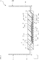
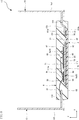
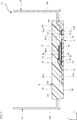
- FIG. 3 is a cross-sectional view taken along the line VII-VII of FIG.
- FIG. 3 is a cross-sectional view taken along the line VII-VII of FIG.
- something A is formed on a certain thing B
- something A is formed on a certain thing B
- something B means “there is a certain thing A” unless otherwise specified. It includes “being formed directly on the object B” and “being formed on the object B with the object A while interposing another object between the object A and the object B”.
- something A is placed on something B” and “something A is placed on something B” means “something A is placed on something B” unless otherwise specified. It includes "being placed directly on B” and “being placed on a certain thing B while having another thing intervening between a certain thing A and a certain thing B".
- something A is located on something B
- something A is in contact with something B and some thing A is on something B
- something B unless otherwise specified.
- What you are doing and "The thing A is located on the thing B while another thing is intervening between the thing A and the thing B”.
- something A overlaps with some thing B when viewed in a certain direction means “something A overlaps with all of some thing B” and “something A overlaps” unless otherwise specified. "Overlapping a part of a certain object B" is included.
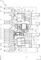
- the semiconductor device A1 of the present embodiment includes a plurality of leads 1, a substrate 2, a plurality of junctions 25, a conductive portion 3, two semiconductor chips 4, two protection elements 9, two control chips 5, and a plurality of control chips 5.
- the passive element 6 includes a plurality of wires 71, 72, 73, 74, and a sealing resin 8, respectively.
- the semiconductor device A1 is an IPM (Intelligent Power Module).
- the semiconductor device A1 is used, for example, in applications such as an air conditioner and a motor control device.
- FIG. 1 is a perspective view showing the semiconductor device A1.
- FIG. 2 is a plan view showing the semiconductor device A1.
- FIG. 3 is a plan view showing the semiconductor device A1 and is a view through which the sealing resin 8 has passed. In FIG. 3, the outer shape of the sealing resin 8 is shown by an imaginary line (dashed line).
- FIG. 4 is a bottom view showing the semiconductor device A1.
- FIG. 5 is a cross-sectional view taken along the line VV of FIG.
- FIG. 6 is a cross-sectional view taken along the line VI-VI of FIG.
- FIG. 7 is a cross-sectional view taken along the line VII-VII of FIG.
- FIG. 8 is a plan view showing the substrate 2.
- the thickness direction of the substrate 2 is the z direction, and the directions along one side of the substrate 2 orthogonal to the z direction (horizontal directions in FIGS. 2 to 4) are orthogonal to the x direction, the z direction, and the x direction.
- the direction (vertical direction in FIGS. 2 to 4) is the y direction.
- the substrate 2 has a rectangular shape in which the shape in the z-direction (also referred to as “planar view”) is long in the x-direction.
- the thickness (dimension in the z direction) of the substrate 2 is, for example, about 0.1 mm to 1.0 mm.
- the dimensions of the substrate 2 are not particularly limited.
- the substrate 2 is made of an insulating material.
- the material of the substrate 2 is not particularly limited.
- the material of the substrate 2 include ceramics such as alumina (Al 2 O 3 ), silicon nitride (SiN), aluminum nitride (AlN), and alumina containing zirconia.
- the substrate 2 has a substrate main surface 21 and a substrate back surface 22.
- the substrate main surface 21 and the substrate back surface 22 are surfaces facing opposite to each other in the z direction, and both are flat surfaces orthogonal to the z direction.
- the substrate main surface 21 is a surface facing upward in FIGS. 5 to 7.
- a conductive portion 3 and a plurality of joint portions 25 are formed on the main surface 21 of the substrate, and a plurality of leads 1 and a plurality of electronic components are mounted.
- the plurality of electronic components include two semiconductor chips 4, two protective elements 9, two control chips 5, and a plurality of passive elements 6.
- the back surface 22 of the substrate is a surface facing downward in FIGS. 5 to 7. As shown in FIG. 4, the back surface 22 of the substrate is exposed from the sealing resin 8.
- the shapes of the substrate main surface 21 and the substrate back surface 22 are both rectangular.
- the shape of the substrate 2 is not particularly limited.
- the conductive portion 3 is formed on the substrate 2.
- the conductive portion 3 is formed on the substrate main surface 21 of the substrate 2.
- the conductive portion 3 is made of a conductive material.
- the conductive material constituting the conductive portion 3 is not particularly limited. Examples of the conductive material of the conductive portion 3 include those containing silver (Ag), copper (Cu), gold (Au) and the like. In the following description, a case where the conductive portion 3 contains silver will be described as an example.
- the conductive portion 3 may contain copper instead of silver, or may contain gold instead of silver or copper. Alternatively, the conductive portion 3 may contain Ag-Pt or Ag-Pd.
- the method for forming the conductive portion 3 is not particularly limited, and the conductive portion 3 is formed, for example, by firing a paste containing these metals.
- the thickness of the conductive portion 3 is not particularly limited, and is, for example, about 5 ⁇ m to 30 ⁇ m.
- the shape of the conductive portion 3 is not particularly limited.
- the conductive portion 3 includes a plurality of pads 31 and a plurality of connection wirings 32, as shown in FIG. 8, for example.
- Each pad 31 has, for example, a rectangular shape, and one of the lead 15 (described later), the control device 50 (described later), the passive element 6, and the wires 72 to 74 is conductively bonded.
- the shape of the pad 31 is not particularly limited.
- the pads 31 are arranged apart from each other.
- the plurality of pads 31 include two pads 31a, 31b, 31c, 31d, and pads 31e, respectively.
- the two pads 31a are arranged side by side in the x direction near the upper right corner of the main surface 21 of the substrate.
- each terminal of the thermistor 6a (described later) is joined to each of the two pads 31a.
- the two pads 31b are arranged side by side in the x direction near the upper left corner of the substrate main surface 21.
- each terminal of the thermistor 6b (described later) is joined to each of the two pads 31b.
- the two pads 31c are arranged near the upper right corner of the substrate main surface 21 between the two pads 31a and the edge of the substrate main surface 21 in the y direction.
- leads 15a (described later) are joined to the two pads 31c, respectively.
- the two pads 31d are arranged near the upper left corner of the substrate main surface 21 between the two pads 31b and the edge of the substrate main surface 21 in the y direction.
- leads 15b (described later) are joined to the two pads 31d, respectively.
- the pad 31e is arranged near the center of the substrate main surface 21.
- a control chip 5b (described later) is joined to the pad 31e.
- connection wiring 32 is connected to a plurality of pads 31 and serves as a conduction path between the connected pads 31. As shown in FIGS. 3 and 8, the plurality of connection wirings 32 include two connection wirings 32a and 32b, respectively. Each connection wiring 32a is connected to the pad 31a and the pad 31c. Each connection wiring 32b is connected to the pad 31b and the pad 31d.
- the plurality of joint portions 25 are formed on the substrate 2.
- the plurality of joints 25 are formed on the substrate main surface 21 of the substrate 2 toward one side (lower side in FIG. 8) in the y direction.
- the material of the joining portion 25 is not particularly limited, and is composed of, for example, a material capable of joining the substrate 2 and the lead 1.
- the joint 25 is made of, for example, a conductive material.
- the conductive material constituting the joint portion 25 is not particularly limited. Examples of the conductive material of the joint portion 25 include those containing silver (Ag), copper (Cu), gold (Au) and the like. In the following description, a case where the joint portion 25 contains silver will be described as an example.
- the joint portion 25 in this example includes the same conductive material as the conductive material constituting the conductive portion 3.
- the joint portion 25 may contain copper instead of silver, or may contain gold instead of silver or copper.
- the joint portion 25 may contain Ag-Pt or Ag-Pd.
- the method for forming the joint portion 25 is not particularly limited, and the joint portion 25 is formed by firing a paste containing these metals, as in the case of the conductive portion 3, for example.
- the thickness of the joint portion 25 is not particularly limited, and is, for example, about 5 ⁇ m to 30 ⁇ m.
- the plurality of joints 25 include the joints 251,252 as shown in FIG.
- the joints 251,252 are separated from each other.
- the joint portion 251 is formed closer to one side (right side in FIG. 8) in the x direction of the substrate 2 in the z direction.
- Leads 11 (described later) are joined to the joint portion 251.
- the joint portion 252 is formed closer to the other side (left side in FIG. 8) in the x direction of the substrate 2 in the z direction.
- Leads 12 (described later) are joined to the joint portion 252.
- the shape and arrangement of the joints 251,252 are not particularly limited.
- the plurality of leads 1 are configured to contain metal, and have a higher thermal conductivity than, for example, the substrate 2.
- the metal constituting the lead 1 is not particularly limited, and is, for example, copper (Cu), aluminum, iron (Fe), oxygen-free copper, or an alloy thereof (for example, Cu—Sn alloy, Cu—Zr alloy, Cu—Fe alloy). Etc.).
- the plurality of leads 1 may be nickel (Ni) plated.
- the plurality of leads 1 may be formed by, for example, pressing a mold against a metal plate, or by patterning the metal plate by etching.
- the method of forming the plurality of leads 1 is not particularly limited.
- the thickness of each lead 1 is not particularly limited, and is, for example, about 0.4 mm to 0.8 mm.
- the leads 1 are separated from each other.
- the plurality of leads 1 includes a lead 11, a lead 12, a lead 13, a lead 14, and a plurality of leads 15.
- the lead 11, lead 12, lead 13, and lead 14 form a conduction path to the semiconductor chip 4, and the side surface of the semiconductor device A1 facing one side in the y direction (lower side in FIGS. 2 and 3). Protruding from.
- the plurality of leads 15 form a conduction path to the control chip 5 or the passive element 6, and project from the side surface of the semiconductor device A1 facing the other side (upper side in FIGS. 2 and 3) in the y direction.
- the lead 11 is arranged on the substrate 2, and in the present embodiment, the lead 11 is arranged on the main surface 21 of the substrate.
- the lead 11 is an example of the “first lead”.
- the lead 11 is joined to the joint portion 25 via the joint material 75.
- the joining material 75 may be any material that can join the leads 11 to the joining portion 25. From the viewpoint of efficiently transferring the heat from the lead 11 to the substrate 2, the bonding material 75 preferably has a higher thermal conductivity, and for example, silver paste, copper paste, solder, or the like is used. However, the bonding material 75 may be an insulating material such as an epoxy resin or a silicone resin. Further, when the bonding portion 25 is not formed on the substrate 2, the lead 11 may be bonded to the substrate 2.
- the configuration of the lead 11 is not particularly limited.
- the lead 11 is divided into a mounting portion 111, a protruding portion 112, an inclined connecting portion 113, and a parallel connecting portion 114.
- the mounting portion 111 has a substantially rectangular shape in the z direction, and has a main surface 111a and a back surface 111b.
- the main surface 111a and the back surface 111b are surfaces facing opposite to each other in the z direction, and both are surfaces orthogonal to the z direction.
- the main surface 111a is a surface facing upward in FIGS. 5 and 6.
- a semiconductor chip 4a and a protective element 9a are mounted on the main surface 111a.
- the back surface 111b is a surface facing downward in FIGS. 5 to 7.
- the back surface 111b is joined to the joint portion 25 by the joint material 75.
- the inclined connecting portion 113 and the parallel connecting portion 114 are covered with the sealing resin 8.
- the inclined connection portion 113 is connected to the mounting portion 111 and the parallel connecting portion 114, and is inclined with respect to the mounting portion 111 and the parallel connecting portion 114.
- the parallel connecting portion 114 is connected to the inclined connecting portion 113 and the protruding portion 112, and is parallel to the mounting portion 111.
- the protruding portion 112 is connected to the end portion of the parallel connecting portion 114, and is a portion of the leads 11 that protrudes from the sealing resin 8.
- the protruding portion 112 protrudes on the side opposite to the mounting portion 111 in the y direction.
- the protrusion 112 is used, for example, to electrically connect the semiconductor device A1 to an external circuit. In the illustrated example, the protrusion 112 is bent in the z direction toward the main surface 111a of the mounting portion 111.
- the lead 12 is arranged on the substrate 2, and in the present embodiment, the lead 12 is arranged on the main surface 21 of the substrate.
- the lead 12 is an example of a “second lead”.
- the lead 12 is joined to the joint portion 25 via the joint material 75.
- the configuration of the lead 12 is not particularly limited. In the present embodiment, as shown in FIG. 7, the lead 12 will be described separately as a mounting portion 121, a protruding portion 122, an inclined connecting portion 123, and a parallel connecting portion 124.
- the mounting portion 121 has a substantially rectangular shape in the z direction, and has a main surface 121a and a back surface 121b.
- the main surface 121a and the back surface 121b are surfaces facing opposite to each other in the z direction, and both are surfaces orthogonal to the z direction.
- the main surface 121a is a surface facing upward in FIG. 7.
- a semiconductor chip 4b and a protective element 9b are mounted on the main surface 121a.
- the back surface 121b is a surface facing downward in FIG. 7.
- the back surface 121b is joined to the joint portion 25 by the joining material 75.
- the inclined connecting portion 123 and the parallel connecting portion 124 are covered with the sealing resin 8.
- the inclined connection portion 123 is connected to the mounting portion 121 and the parallel connecting portion 124, and is inclined with respect to the mounting portion 121 and the parallel connecting portion 124.
- the parallel connecting portion 124 is connected to the inclined connecting portion 123 and the protruding portion 122, and is parallel to the mounting portion 121.
- the protruding portion 122 is connected to the end portion of the parallel connecting portion 124, and is a portion of the leads 12 that protrudes from the sealing resin 8.
- the protruding portion 122 protrudes on the side opposite to the mounting portion 121 in the y direction.
- the protrusion 122 is used, for example, to electrically connect the semiconductor device A1 to an external circuit. In the illustrated example, the protrusion 122 is bent in the z direction toward the main surface 121a of the mounting portion 121.
- the lead 13 is not arranged on the substrate 2 and is supported by the sealing resin 8.
- the lead 13 does not include a portion corresponding to the mounting portion 111 and the inclined connecting portion 113 of the lead 11.
- the configuration of the lead 13 is not limited to this. In the present embodiment, as shown in FIG. 6, the lead 13 will be described by dividing it into a protruding portion 132 and a wire bonding portion 134.
- the wire bonding portion 134 is covered with the sealing resin 8.
- a wire 71 is bonded to the wire bonding portion 134.
- the protruding portion 132 is connected to the end portion of the wire bonding portion 134 and is a portion of the lead 13 that protrudes from the sealing resin 8.
- the protruding portion 132 projects in the y direction on the side opposite to the mounting portion 111 of the lead 11.
- the protrusion 132 is used, for example, to electrically connect the semiconductor device A1 to an external circuit. In the illustrated example, the protrusion 132 is bent in the z direction toward the main surface 111a of the lead 11.
- the lead 14 is not arranged on the substrate 2 and is supported by the sealing resin 8.
- the lead 14 has the same configuration as the lead 13.
- the configuration of the lead 14 is not limited to this.
- the lead 14 will be described separately as a protrusion 142 and a wire bonding portion 144.
- the wire bonding portion 144 is covered with the sealing resin 8.
- a wire 71 is bonded to the wire bonding portion 144.
- the protruding portion 142 is connected to the end portion of the wire bonding portion 144, and is a portion of the leads 14 that protrudes from the sealing resin 8.
- the protruding portion 142 projects in the y direction on the side opposite to the mounting portion 111 of the lead 11.
- the protrusion 142 is used, for example, to electrically connect the semiconductor device A1 to an external circuit. In the illustrated example, the protrusion 142 is bent in the z direction toward the main surface 111a of the lead 11.
- the plurality of leads 15 are respectively arranged on the substrate 2, and in the present embodiment, they are arranged on the main surface 21 of the substrate.
- Each lead 15 is an example of a “control lead”.
- Each lead 15 is bonded to the pad 31 of the conductive portion 3 via the conductive bonding material 76.
- the conductive bonding material 76 may be any material that can bond the lead 15 to the pad 31 and electrically connect the lead 15 and the pad 31.
- As the conductive bonding material 76 for example, silver paste, copper paste, solder, or the like is used.
- the configuration of the lead 15 is not particularly limited. In the present embodiment, as shown in FIGS. 5 to 7, the lead 15 will be described by dividing it into a joint portion 151, a protruding portion 152, an inclined connecting portion 153, and a parallel connecting portion 154.
- the joint portion 151 has a main surface 151a and a back surface 151b.
- the main surface 151a and the back surface 151b are surfaces facing opposite to each other in the z direction, and both are flat surfaces orthogonal to the z direction.
- the main surface 151a is a surface facing upward in FIGS. 5 to 75.
- the back surface 151b is a surface facing downward in FIGS. 5 to 7.
- the back surface 151b is bonded to the pad 31 by the conductive bonding material 76.
- the inclined connecting portion 153 and the parallel connecting portion 154 are covered with the sealing resin 8.
- the inclined connection portion 153 is connected to the joint portion 151 and the parallel connection portion 154, and is inclined with respect to the joint portion 151 and the parallel connection portion 154.
- the parallel connection portion 154 is connected to the inclined connection portion 153 and the protrusion portion 152, and is parallel to the joint portion 151.
- the protruding portion 152 is connected to the end portion of the parallel connecting portion 154 and is a portion of the leads 15 that protrudes from the sealing resin 8.
- the protruding portion 152 protrudes on the side opposite to the joint portion 151 in the y direction.
- the protrusion 152 is used, for example, to electrically connect the semiconductor device A1 to an external circuit. In the illustrated example, the protrusion 152 is bent in the z direction toward the main surface 151a of the joint portion 151.
- the plurality of leads 15 include two leads 15a and 15b, respectively.
- the two leads 15a are conductively bonded to different pads 31c.
- the two leads 15b are conductively bonded to different pads 31d.
- Each of the two semiconductor chips 4 is arranged on one of the leads 1.
- a semiconductor chip 4a When two semiconductor chips 4 are described separately, one is referred to as a semiconductor chip 4a and the other is referred to as a semiconductor chip 4b. When the two are not distinguished, the semiconductor chip 4 is simply used.
- the type and function of the semiconductor chip 4 are not particularly limited, and in the present embodiment, the case where the semiconductor chip 4 is a power transistor for controlling electric power will be described as an example.
- the semiconductor chip 4 is, for example, a MOSFET (metal-oxide-semiconductor field-effect transistor) made of a SiC (silicon carbide) substrate.
- MOSFET metal-oxide-semiconductor field-effect transistor
- the semiconductor chip 4 may be a MOSFET made of a Si (silicon) substrate instead of the SiC substrate, and may include, for example, an IGBT element. Further, it may be a MOSFET containing GaN (gallium nitride).
- the semiconductor chip 4 has a plate-like rectangular shape in the z-direction, and includes an element main surface 41, an element back surface 42, a source electrode 43, a gate electrode 44, and a drain electrode 45.
- the element main surface 41 and the element back surface 42 face opposite to each other in the z direction.
- the element main surface 41 is a surface facing upward in FIGS. 5 to 7.
- the back surface 42 of the element is a surface facing downward in FIGS. 5 to 7.
- a source electrode 43 and a gate electrode 44 are arranged on the element main surface 41.
- a drain electrode 45 is arranged on the back surface 42 of the element.
- the shapes and arrangements of the source electrode 43, the gate electrode 44, and the drain electrode 45 are not particularly limited.
- the semiconductor chip 4a is arranged on the lead 11 as shown in FIGS. 3, 5 and 6. As shown in FIGS. 5 and 6, the semiconductor chip 4a is joined to the lead 11 by a conductive bonding material (not shown) with the back surface 42 of the element facing the lead 11. As a result, the drain electrode 45 of the semiconductor chip 4a is electrically connected to the lead 11 by the conductive bonding material.
- the conductive bonding material for example, silver paste, copper paste, solder or the like is used.
- the source electrode 43 of the semiconductor chip 4a is electrically connected to the lead 13 by the wire 71.
- the wire 71 is made of, for example, aluminum (Al) or copper (Cu).
- the material, wire diameter, and number of wires 71 are not particularly limited.
- the semiconductor chip 4b is arranged on the lead 12 as shown in FIGS. 3 and 7. As shown in FIG. 7, the semiconductor chip 4b is joined to the lead 12 by a conductive bonding material (not shown) with the back surface 42 of the element facing the lead 12. As a result, the drain electrode 45 of the semiconductor chip 4b is electrically connected to the lead 12 by the conductive bonding material. Further, as shown in FIG. 3, the source electrode 43 of the semiconductor chip 4b is electrically connected to the lead 14 by the wire 71.
- the gate electrode 44 of the semiconductor chip 4a is connected to the conductive portion 3 by the wire 72, and is electrically connected to the control chip 5a (described later). Further, the source electrode 43 of the semiconductor chip 4a is connected to the conductive portion 3 by the wire 73, and is electrically connected to the control chip 5a.
- the wires 72 and 73 are made of, for example, gold (Au), silver (Ag), copper (Cu), aluminum (Al), or the like. The material, wire diameter, and number of wires 72 and 73 are not particularly limited.
- the control chip 5a inputs a drive signal to the gate electrode 44 of the semiconductor chip 4a. Further, the gate electrode 44 of the semiconductor chip 4b is connected to the conductive portion 3 by the wire 72, and is electrically connected to the control chip 5b.
- the control chip 5b inputs a drive signal to the gate electrode 44 of the semiconductor chip 4b.
- the semiconductor device A1 is used as a bridge circuit in which leads 12 and leads 13 are electrically connected externally, the semiconductor chip 4a is used as a switching element on the upper stage side, and the semiconductor chip 4b is used as a switching element on the lower stage side.
- a DC voltage is applied between the lead 11 and the lead 14, and the drive signal is input to the gate electrodes 44 of the semiconductor chips 4a and 4b, so that the voltage is switched according to the drive signal.
- the switching signal is output from the lead 12.
- Each of the two protective elements 9 is arranged on one of the leads 1.
- a protective element 9a When the two protective elements 9 are described separately, one is referred to as a protective element 9a and the other is referred to as a protective element 9b. When the two are not distinguished, the protection element 9 is simply used.
- the type and function of the protective element 9 are not particularly limited, and in the present embodiment, a case where the protective element 9 is a diode for preventing a reverse voltage from being applied to the semiconductor chip 4 will be described as an example.
- the protective element 9 has a plate-like rectangular shape in the z-direction, and includes a protective element main surface 91, a protective element back surface 92, an anode electrode 93, and a cathode electrode 94.
- the main surface 91 of the protective element and the back surface 92 of the protective element face each other in the z direction.
- the protective element main surface 91 is a surface facing upward in FIGS. 5 and 6.
- the back surface 92 of the protective element is a surface facing downward in FIGS. 5 and 6.
- an anode electrode 93 is arranged on the main surface 91 of the protective element.
- a cathode electrode 94 is arranged on the back surface 92 of the protective element.
- the shapes and arrangements of the anode electrode 93 and the cathode electrode 94 are not particularly limited.
- the protective element 9a is arranged on the lead 11 on one side (lower side in FIG. 3) of the semiconductor chip 4a in the y direction. As shown in FIGS. 5 and 6, the protective element 9a is joined to the lead 11 by a conductive bonding material (not shown) with the back surface 92 of the protective element facing the lead 11. As a result, the cathode electrode 94 of the protective element 9a is electrically connected to the lead 11 by the conductive bonding material.
- the conductive bonding material for example, silver paste, copper paste, solder or the like is used.
- the cathode electrode 94 of the protective element 9a and the drain electrode 45 of the semiconductor chip 4a are conductively connected via the lead 11.
- the anode electrode 93 of the protective element 9a is electrically connected to the semiconductor chip 4a and the lead 13 by the wire 71.
- one end of the wire 71 is bonded to the source electrode 43 of the semiconductor chip 4a, the intermediate portion is bonded to the anode electrode 93 of the protective element 9a, and the other end is bonded to the lead 13.
- the source electrode 43 and the anode electrode 93 may be connected by a wire 71, and the anode electrode 93 and the lead 13 may be connected by another wire 71. Further, the source electrode 43 and the lead 13 may be connected by a wire 71, and the anode electrode 93 and the lead 13 may be connected by another wire 71.
- the protection element 9a is connected in antiparallel to the semiconductor chip 4a.
- the protective element 9b is arranged on the lead 12 on one side (lower side in FIG. 3) of the semiconductor chip 4b in the y direction.
- the protective element 9b is joined to the lead 12 by a conductive bonding material (not shown) with the back surface 92 of the protective element facing the lead 12.
- the cathode electrode 94 of the protective element 9b is electrically connected to the lead 12 by the conductive bonding material.
- the cathode electrode 94 of the protective element 9b and the drain electrode 45 of the semiconductor chip 4b are conductively connected via the lead 12.
- the anode electrode 93 of the protective element 9b is electrically connected to the semiconductor chip 4b and the lead 14 by the wire 71.
- one end of the wire 71 is bonded to the source electrode 43 of the semiconductor chip 4b, the intermediate portion is bonded to the anode electrode 93 of the protective element 9b, and the other end is bonded to the lead 14.
- the source electrode 43 and the anode electrode 93 may be connected by a wire 71, and the anode electrode 93 and the lead 14 may be connected by another wire 71. Further, the source electrode 43 and the lead 14 may be connected by a wire 71, and the anode electrode 93 and the lead 13 may be connected by another wire 71.
- the protection element 9b is connected in antiparallel to the semiconductor chip 4b.
- the semiconductor device A1 does not have to include the protection element 9.
- Each of the two control chips 5 controls the drive of the semiconductor chip 4, and is arranged on the substrate main surface 21 of the substrate 2.
- the two control chips 5 are described separately, one is referred to as a control chip 5a and the other is referred to as a control chip 5b.
- the control chip 5 is simply used.
- control chip 5a and the control chip 5b are arranged between the lead 11 and the lead 12, separated from the lead 11 and the lead 12.
- the control chip 5a is located closer to the lead 11, and the control chip 5b is located closer to the lead 12.
- the arrangement of the control chip 5a and the control chip 5b is not particularly limited.
- the control chip 5a controls the drive of the semiconductor chip 4a. Specifically, the control chip 5a drives the semiconductor chip 4a by generating a drive signal and inputting the drive signal to the gate electrode 44 of the semiconductor chip 4a.
- the control chip 5a constitutes a control device 50 together with a die pad (not shown), a plurality of wires, a plurality of leads 53, and a resin 54.
- the die pad and the plurality of leads 53 are plate-shaped members made of, for example, copper (Cu).
- the die pad is equipped with a control chip 5a. Each lead 53 is conducted to the control chip 5a by a wire.
- the resin 54 covers the entire control chip 5a and the wire, and a part of each lead 53, and is made of an insulating material such as an epoxy resin or a silicone gel.
- the leads 53 are arranged at both ends of the resin 54 in the y direction at intervals in the x direction.
- Each lead 53 extends along the y direction, and a part of each protrudes from both side surfaces of the resin 54 in the y direction.
- a portion of each lead 53 protruding from the resin 54 is conductively bonded to the pad 31 of the conductive portion 3.
- the control device 50 is a SOP (Small Outline Package) type package.
- the package type of the control device 50 is not limited to the SOP type, and may be another type of package such as a QFP (Quad Flat Package) type or a SOJ (Small Outline J-lead Package) type.
- the size, shape, number of leads, etc. of the control device 50 are not particularly limited. Further, the control device 50 may include a circuit chip other than the control chip 5a.
- the control chip 5b controls the drive of the semiconductor chip 4b. Specifically, the control chip 5b drives the semiconductor chip 4b by generating a drive signal and inputting it to the gate electrode 44 of the semiconductor chip 4b.
- the control chip 5b is arranged as it is on the main surface 21 of the substrate. One surface of the control chip 5b is joined to the pad 31c, and a plurality of electrodes arranged on the other surface are electrically connected to the pad 31 by wires 74.
- the wire 74 is made of, for example, gold (Au), silver (Ag), copper (Cu), aluminum (Al), or the like.
- the material, wire diameter, and number of wires 74 are not particularly limited.
- the control chip 5a may be arranged on the main surface 21 of the substrate as it is, similarly to the control chip 5b. Further, the control chip 5b may be arranged on the substrate main surface 21 as the control device 50 in the same manner as the control chip 5a.
- the plurality of passive elements 6 are arranged on the substrate main surface 21 of the substrate 2 and are conductively bonded to the pad 31 of the conductive portion 3.
- the passive element 6 is, for example, a resistor, a capacitor, a coil, a diode, or the like.
- the passive element 6 includes a thermistor 6a and a thermistor 6b.
- Thermistors 6a and 6b are temperature detection elements and are mounted on the main surface 21 of the substrate 2.
- the thermistors 6a and 6b are resistors whose electrical resistance changes greatly with respect to temperature changes, and the voltage between terminals changes as the resistance value changes according to the ambient temperature.
- the ambient temperature of the thermistors 6a and 6b is detected based on the voltage between the terminals of the thermistors 6a and 6b.
- the characteristics of the thermistors 6a and 6b are not particularly limited.
- the thermistors 6a and 6b may be NTC (negative temperature coefficient) thermistors, PTC (Positive temperature coefficient) thermistors, or thermistors having other characteristics.
- the thermistor 6a is for detecting the temperature of the semiconductor chip 4a, and is arranged adjacent to the mounting portion 111 of the lead 11 on which the semiconductor chip 4a is mounted, as shown in FIG.
- the thermistor 6a is insulated from the lead 11.
- the thermistor 6a is arranged so as to straddle the two pads 31a of the conductive portion 3.
- One terminal of the thermistor 6a is conductively bonded to one pad 31a, and the other terminal is conductively bonded to the other pad 31a.
- Each pad 31a is electrically connected to the lead 15a via the connection wiring 32a and the pad 31c, respectively.
- the pad 31a, the connection wiring 32a, and the pad 31c are conduction paths that conduct the thermistor 6a and the lead 15a.
- the two leads 15a serve as terminals for detecting the temperature of the semiconductor chip 4a, and output the voltage between the terminals of the thermistor 6a.
- the thermistor 6a is an example of the "first temperature detecting element".
- the thermistor 6b is for detecting the temperature of the semiconductor chip 4b, and is arranged adjacent to the mounting portion 121 of the lead 12 on which the semiconductor chip 4b is mounted, as shown in FIG.
- the thermistor 6b is insulated from the lead 12.
- the thermistor 6b is arranged so as to straddle the two pads 31b of the conductive portion 3.
- One terminal of the thermistor 6b is conduction-bonded to one pad 31b, and the other terminal is conduction-bonded to the other pad 31b.
- Each pad 31b is electrically connected to the lead 15b via the connection wiring 32b and the pad 31d, respectively.
- the pad 31b, the connection wiring 32b, and the pad 31d are conduction paths that conduct the thermistor 6b and the lead 15b.
- the two leads 15b serve as terminals for detecting the temperature of the semiconductor chip 4b, and output the voltage between the terminals of the thermistor 6b.
- the thermistor 6b is an example of the "second temperature detecting element".
- the semiconductor device A1 may be provided with another temperature detecting element instead of the thermistors 6a and 6b.
- a semiconductor temperature sensor or the like can be considered.
- the semiconductor temperature sensor is a Si diode or the like whose forward voltage changes greatly with respect to a temperature change, and the ambient temperature is detected based on the voltage between terminals when a predetermined current is passed.
- the other passive element 6 is conductively bonded to the pad 31 of the conductive portion 3 and is electrically connected to the control chip 5 or the semiconductor chip 4 via the connection wiring 32 and the pad 31.
- the type, arrangement position, and number of each passive element 6 are not particularly limited.
- the sealing resin 8 includes semiconductor chips 4a and 4b, protective elements 9a and 9b, a control device 50 (control chip 5a), a control chip 5b, a plurality of passive elements 6, and wires 71 to 74, and one of a plurality of leads 1. It covers at least a portion and a part of the substrate 2.
- the material of the sealing resin 8 is not particularly limited, and for example, an insulating material such as an epoxy resin or a silicone gel is appropriately used.
- the sealing resin 8 has a resin main surface 81, a resin back surface 82, and four resin side surfaces 83.
- the resin main surface 81 and the resin back surface 82 are surfaces facing opposite to each other in the z direction, and both are flat surfaces orthogonal to the z direction.
- the resin main surface 81 is a surface facing upward in FIGS. 5 to 7.
- the resin back surface 82 is a surface facing downward in FIGS. 5 to 7.
- Each resin side surface 83 is connected to the resin main surface 81 and the resin back surface 82, and faces the x direction or the y direction, respectively.
- the substrate back surface 22 of the substrate 2 is exposed from the resin back surface 82 of the sealing resin 8.
- the back surface 22 of the substrate and the back surface 82 of the resin are flush with each other.
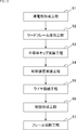
- the manufacturing method of this example includes a conductive portion forming step (step S1), a lead frame joining step (step S2), a semiconductor chip mounting step (step S3), and a control device mounting step (step S4). It has a wire connecting step (step S5), a resin forming step (step S6), and a frame cutting step (step S7).
- the substrate 2 is prepared.
- the substrate 2 is made of, for example, ceramic.
- the conductive portion 3 and the plurality of joint portions 25 are formed on the substrate main surface 21 of the substrate 2.
- the conductive portion 3 and the plurality of joint portions 25 are collectively formed. For example, by printing a metal paste and then firing it, a conductive portion 3 and a plurality of joint portions 25 containing a metal such as silver (Ag) as a conductive material can be obtained.
- the joining paste is printed on a plurality of joining portions 25, and the conductive joining paste is printed on a part of the pads 31 of the conductive portion 3.
- the bonding paste and the conductive bonding paste are, for example, Ag paste and solder paste.
- a lead frame is prepared.
- the lead frame includes a plurality of leads 1, and further includes a frame in which the plurality of leads 1 are connected.
- the shape of the lead frame is not limited at all.
- the leads 11 and 12 of the plurality of leads 1 are made to face the plurality of joint portions 25 via the bonding paste.
- a plurality of leads 15 among the plurality of leads 1 are made to face the conductive portion 3 (pad 31) via the conductive bonding paste.
- the bonding material 75 is formed by the bonding paste
- the conductive bonding material 76 is formed by the conductive bonding paste.
- the conductive bonding paste is printed at predetermined positions of the leads 11 and the leads 12.
- the conductive bonding paste is, for example, Ag paste or solder paste.
- the semiconductor chip 4a and the protective element 9a are attached to the conductive bonding paste printed on the lead 11, and the semiconductor chip 4b and the protective element 9b are attached to the conductive bonding paste printed on the lead 12.
- a conductive bonding material is formed by the conductive bonding paste.
- the semiconductor chip 4a and the protective element 9a are bonded to the lead 11 via the conductive bonding material
- the semiconductor chip 4b and the protective element 9b are bonded to the lead 12 via the conductive bonding material.
- the conductive bonding paste is printed on a part of the pads 31 of the conductive portion 3.
- the conductive bonding paste is, for example, Ag paste or solder paste.
- each lead 53 of the control device 50 is attached to the conductive bonding paste.
- the control chip 5b is attached to the conductive bonding paste printed on the pad 31e.
- each lead 53 and the control chip 5b of the control device 50 are bonded to the pad 31 via the conductive bonding material.
- the thermistors 6a and 6b and other passive elements 6 are joined to the pad 31 of the conductive portion 3 via the conductive bonding material.
- a plurality of wires 71 are connected.
- wire materials made of aluminum (Al) are sequentially connected by, for example, a wedge bonding method.
- the tip of the wire material is bonded to the source electrode 43 of the semiconductor chip 4a, the capillary is moved while pulling out the wire material, the wire material is bonded to the anode electrode 93 of the protective element 9a, and the wire material is further bonded.
- the wire 71 is connected by moving the capillary while pulling out and joining the wire material to the wire bonding portion 134 of the lead 13.
- the wire 71 is connected by sequentially joining the wire material to the source electrode 43 of the semiconductor chip 4b, the anode electrode 93 of the protective element 9b, and the wire bonding portion 144 of the lead 14. As a result, a plurality of wires 71 can be obtained.
- the plurality of wires 72, 73, 74 are connected.
- wire materials made of gold (Au) are sequentially connected by, for example, a capillary bonding method. As a result, a plurality of wires 72, 73, 74 can be obtained.
- step S6 for example, a part of the lead frame, a part of the substrate 2, semiconductor chips 4a and 4b, protective elements 9a and 9b, a control device 50 (control chip 5a), a control chip 5b, and a plurality of passives.
- the element 6 and the plurality of wires 71 to 74 are surrounded by a mold.
- the liquid resin material is injected into the space defined by the mold.
- the sealing resin 8 is obtained.
- step S7 the appropriate part of the lead frame exposed from the sealing resin 8 is cut. As a result, the plurality of leads 1 are divided into each other. After that, the semiconductor device A1 described above can be obtained by undergoing a process such as bending a plurality of leads 1 as needed.
- the thermistor 6a is arranged adjacent to the mounting portion 111 of the lead 11 on which the semiconductor chip 4a is mounted, and detects the temperature of the semiconductor chip 4a.
- the thermistor 6b is arranged adjacent to the mounting portion 121 of the lead 12 on which the semiconductor chip 4b is mounted, and detects the temperature of the semiconductor chip 4b. Therefore, even if the flowing currents of the semiconductor chip 4a and the semiconductor chip 4b are biased and a temperature difference occurs, the temperature can be detected individually and compared with the design temperature, so that thermal runaway can be suppressed.
- the thermistors 6a and 6b are mounted on the substrate main surface 21 of the substrate 2. Therefore, the thermistors 6a and 6b are less susceptible to noise due to switching of the semiconductor chips 4a and 4b as compared with the case where the temperature detection unit is incorporated inside the semiconductor chips 4a and 4b.
- the conductive portion 3 is formed on the substrate main surface 21 of the substrate 2.
- the control device 50 and the control chip 5b are conductively joined to the pad 31.
- the conduction path to the control device 50 and the control chip 5b can be configured by the conductive portion 3 formed on the main surface 21 of the substrate. Therefore, as compared with the case where the conduction path is formed by, for example, a metal lead, it is possible to make the conduction path thinner and have a higher density.
- the semiconductor chip 4a is directly bonded to the lead 11 by the conductive bonding material, and the semiconductor chip 4b is directly bonded to the lead 12 by the conductive bonding material. Therefore, the semiconductor chip 4a (4b) and the lead 11 (12) can be made conductive, and the heat from the semiconductor chip 4a (4b) can be transferred to the lead 11 (12) more efficiently.
- a conduction path from the outside to the semiconductor chip 4 can be formed, and the heat dissipation characteristics of the semiconductor chip 4 can be further secured.
- a bonding portion 25 is formed on the substrate 2, and leads 11 and 12 are bonded to the substrate 2 via the bonding portion 25.
- the surface of the joint portion 25 can be finished more smoothly than the surface roughness of the substrate main surface 21 of the substrate 2 made of ceramic.
- the back surface 22 of the substrate 2 is exposed from the sealing resin 8. As a result, the heat transferred from the semiconductor chip 4 or the like to the substrate 2 can be more efficiently dissipated to the outside.
- the conductive portion 3 and the joint portion 25 contain the same conductive material, the conductive portion 3 and the joint portion 25 can be collectively formed on the substrate 2. This is preferable for improving the manufacturing efficiency of the semiconductor device A1.
- the plurality of leads 15 are joined to the pad 31 of the conductive portion 3 via the conductive bonding material 76. As a result, the plurality of leads 15 can be more firmly fixed to the substrate 2. Further, it is possible to reduce the resistance between the plurality of leads 15 and the conductive portion 3.
- control chip 5a and the control chip 5b are arranged on the substrate main surface 21 between the lead 11 on which the semiconductor chip 4a is arranged and the lead 12 on which the semiconductor chip 4b is arranged. .. Therefore, the difference between the distance from the control chip 5a to the semiconductor chip 4a and the distance from the control chip 5b to the semiconductor chip 4b can be reduced. As a result, the difference in transmission time between the drive signal input from the control chip 5a to the semiconductor chip 4a and the drive signal input from the control chip 5b to the semiconductor chip 4b can be reduced.
- the semiconductor device A1 includes two temperature detecting elements, a thermistor 6a for detecting the temperature of the semiconductor chip 4a and a thermistor 6b for detecting the temperature of the semiconductor chip 4b.
- the semiconductor device A1 may include more than the number of temperature detecting elements of the semiconductor chips 4.
- FIG. 10 is a diagram for explaining the semiconductor device A2 according to the second embodiment of the present disclosure.
- FIG. 10 is a plan view showing the semiconductor device A2, and is a diagram corresponding to FIG.
- the sealing resin 8 is passed through, and the outer shape of the sealing resin 8 is shown by an imaginary line (dashed line).
- the arrangement positions of the thermistor 6a and the thermistor 6b and the shapes of the leads 11 and 12 are different from those of the first embodiment.
- the thermistor 6a and the thermistor 6b are arranged closer to one edge (upper edge in FIG. 10) of the substrate main surface 21 in the y direction than in the case of the semiconductor device A1. ing. That is, as compared with the semiconductor device A1, the thermistor 6a is arranged away from the mounting portion 111 of the lead 11, and the thermistor 6b is arranged away from the mounting portion 121 of the lead 12.
- the lead 11 further includes an extending portion 115 extending from the mounting portion 111 toward the thermistor 6a along the y direction. That is, the thermistor 6a is arranged near the tip of the extending portion 115. The thermistor 6a is kept away from the mounting portion 111 and the semiconductor chip 4a mounted on the mounting portion 111, but is adjacent to the lead 11 due to the presence of the extending portion 115. Therefore, the heat generated by the semiconductor chip 4a is transmitted to the thermistor 6a via the lead 11.
- the lead 12 further includes an extension portion 125 extending from the mounting portion 121 toward the thermistor 6b along the y direction. That is, the thermistor 6b is arranged near the tip of the extension portion 125. The thermistor 6b is kept away from the mounting portion 121 and the semiconductor chip 4b mounted on the mounting portion 121, but is adjacent to the lead 12 due to the presence of the extending portion 125. Therefore, the heat generated by the semiconductor chip 4b is transmitted to the thermistor 6b via the lead 12.
- the thermistor 6a is arranged adjacent to the extending portion 115 extending from the mounting portion 111 of the lead 11 on which the semiconductor chip 4a is mounted, and detects the temperature of the semiconductor chip 4a.
- the thermistor 6b is arranged adjacent to the extending portion 125 extending from the mounting portion 121 of the lead 12 on which the semiconductor chip 4b is mounted, and detects the temperature of the semiconductor chip 4b. Therefore, since the temperature is detected individually, it is possible to suppress thermal runaway. Further, since the thermistors 6a and 6b are mounted on the substrate main surface 21 of the substrate 2, they are not easily affected by noise due to switching of the semiconductor chips 4a and 4b.
- the thermistor 6a (6b) is further away from the semiconductor chip 4a (4b) as compared with the semiconductor device A1. Therefore, the thermistors 6a and 6b are less susceptible to noise due to switching of the semiconductor chips 4a and 4b.
- FIG. 11 is a diagram for explaining the semiconductor device A3 according to the third embodiment of the present disclosure.
- FIG. 11 is a plan view showing the semiconductor device A3, and is a diagram corresponding to FIG.
- the sealing resin 8 is passed through, and the outer shape of the sealing resin 8 is shown by an imaginary line (dashed line).
- the arrangement positions of the semiconductor chip 4 and the protective element 9 are different from those of the first embodiment.
- the arrangement positions of the semiconductor chip 4a and the protection element 9a are opposite, and the arrangement positions of the semiconductor chip 4b and the protection element 9b are opposite. That is, the protective element 9a is arranged on the lead 11 on the other side of the semiconductor chip 4a in the y direction (upper side in FIG. 11), and the protective element 9b is placed on the lead 12 in the y direction of the semiconductor chip 4b. It is located on the other side. That is, the thermistor 6a is arranged on the side opposite to the semiconductor chip 4a with respect to the protection element 9a, and the thermistor 6b is arranged on the side opposite to the semiconductor chip 4b with respect to the protection element 9b.
- the thermistor 6a is arranged adjacent to the mounting portion 111 of the lead 11 on which the semiconductor chip 4a is mounted, and detects the temperature of the semiconductor chip 4a.
- the thermistor 6b is arranged adjacent to the mounting portion 121 of the lead 12 on which the semiconductor chip 4b is mounted, and detects the temperature of the semiconductor chip 4b. Therefore, since the temperature is detected individually, it is possible to suppress thermal runaway. Further, since the thermistors 6a and 6b are mounted on the substrate main surface 21 of the substrate 2, they are not easily affected by noise due to switching of the semiconductor chips 4a and 4b.
- the thermistor 6a (6b) is further away from the semiconductor chip 4a (4b) as compared with the semiconductor device A1. Therefore, the thermistors 6a and 6b are less susceptible to noise due to switching of the semiconductor chips 4a and 4b.
- FIG. 12 is a diagram for explaining the semiconductor device A4 according to the fourth embodiment of the present disclosure.
- FIG. 12 is a plan view showing the semiconductor device A4, and is a diagram corresponding to FIG. In FIG. 12, similarly to FIG. 3, the sealing resin 8 is passed through, and the outer shape of the sealing resin 8 is shown by an imaginary line (dashed line).
- the semiconductor device A4 of the present embodiment is different from the first embodiment in that it includes a control device 50 having one control chip 5c instead of the control device 50 (control chip 5a) and the control chip 5b. There is.
- the control chip 5c generates a drive signal of the semiconductor chip 4a and a drive signal of the semiconductor chip 4b, and outputs the drive signal to each of them.
- the control chip 5c constitutes the control device 50 together with a die pad (not shown), a plurality of wires, a plurality of leads 53, and a resin 54.
- the leads 53 are arranged at both ends of the resin 54 in the x direction at intervals in the y direction.
- Each lead 53 extends along the x direction, and a part of each protrudes from both side surfaces of the resin 54 in the x direction.
- a portion of each lead 53 protruding from the resin 54 is conductively bonded to the pad 31 of the conductive portion 3.
- the control device 50 is a SOP type package.
- the package type of the control device 50 is not particularly limited.
- the control chip 5c may be arranged on the main surface 21 of the substrate as it is without forming the control device 50.
- the semiconductor device A4 according to the fourth embodiment adopts the control device 50 having the control chip 5c, so that the arrangement and shape of each passive element 6 and the conductive portion 3 are different from those of the semiconductor device A1. There is. Further, the shapes of the leads 13 and 14 and the shapes and arrangements of the leads 15a and 15b are also different.
- the thermistor 6a is arranged adjacent to the mounting portion 111 of the lead 11 on which the semiconductor chip 4a is mounted, and detects the temperature of the semiconductor chip 4a.
- the thermistor 6b is arranged adjacent to the mounting portion 121 of the lead 12 on which the semiconductor chip 4b is mounted, and detects the temperature of the semiconductor chip 4b. Therefore, since the temperature is detected individually, it is possible to suppress thermal runaway. Further, since the thermistors 6a and 6b are mounted on the substrate main surface 21 of the substrate 2, they are not easily affected by noise due to switching of the semiconductor chips 4a and 4b.
- FIG. 13 is a diagram for explaining the semiconductor device A5 according to the fifth embodiment of the present disclosure.
- FIG. 13 is a partial plan view showing the semiconductor device A5, and is a view through which the sealing resin 8 has passed.
- the outer shape of the sealing resin 8 is shown by an imaginary line (dashed line).
- the semiconductor device A5 of the present embodiment is different from the first embodiment in that it includes four semiconductor chips 4a to 4d.
- the semiconductor device A5 further includes leads 16 to 19, semiconductor chips 4c and 4d, and thermistors 6c and 6d as compared with the semiconductor device A1. Further, the semiconductor device A5 includes two control chips 5c according to the third embodiment.
- the leads 16 and 17 are the same as the leads 11 and 12.
- the leads 18 and 19 are the same as the leads 13 and 14.
- the semiconductor chips 4c and 4d are the same as the semiconductor chips 4a and 4b.
- the semiconductor chip 4c is mounted on the lead 16 and is connected to the lead 18 by a wire 71.
- the semiconductor chip 4d is mounted on the lead 17 and is connected to the lead 19 by a wire 71.
- control chip 5c controls the driving of the semiconductor chips 4a and 4b by generating a driving signal of the semiconductor chip 4a and a driving signal of the semiconductor chip 4b and outputting them to each of them.
- the other control chip 5c controls the driving of the semiconductor chips 4c and 4d by generating a driving signal of the semiconductor chip 4c and a driving signal of the semiconductor chip 4d and outputting them to each of them.
- Thermistors 6c and 6d are the same as the thermistors 6a and 6b.
- the thermistor 6c is arranged adjacent to the mounting portion of the lead 16 on which the semiconductor chip 4c is mounted, and detects the temperature of the semiconductor chip 4c.
- the thermistor 6d is arranged adjacent to the mounting portion of the lead 17 on which the semiconductor chip 4d is mounted, and detects the temperature of the semiconductor chip 4d. That is, since the semiconductor device A5 has four semiconductor chips, it is provided with four thermistors for detecting each temperature.
- the thermistor 6a is arranged adjacent to the mounting portion 111 of the lead 11 on which the semiconductor chip 4a is mounted, and detects the temperature of the semiconductor chip 4a.
- the thermistor 6b is arranged adjacent to the mounting portion 121 of the lead 12 on which the semiconductor chip 4b is mounted, and detects the temperature of the semiconductor chip 4b.
- the thermistor 6c is arranged adjacent to the mounting portion of the lead 16 on which the semiconductor chip 4c is mounted, and detects the temperature of the semiconductor chip 4c.
- the thermistor 6d is arranged adjacent to the mounting portion of the lead 17 on which the semiconductor chip 4d is mounted, and detects the temperature of the semiconductor chip 4d. Therefore, since the temperature is detected individually, it is possible to suppress thermal runaway. Further, since the thermistors 6a to 6d are mounted on the substrate main surface 21 of the substrate 2, they are not easily affected by noise due to switching of the semiconductor chips 4a to 4d.
- the number of semiconductor chips may be three or five or more.
- the number of thermistors may be adjusted to match the number of semiconductor chips. Further, the number of thermistors may be larger than the number of semiconductor chips.
- FIG. 14 is a diagram for explaining the semiconductor device A6 according to the sixth embodiment of the present disclosure.
- FIG. 14 is a plan view showing the semiconductor device A6, and is a view through which the sealing resin 8 has passed.
- the outer shape of the sealing resin 8 is shown by an imaginary line (dashed line).
- the semiconductor device A6 of the present embodiment is different from the first embodiment in that the semiconductor chips 4a and 4b are arranged in the conductive portion 3 without being mounted on the lead 1.
- the conductive portion 3 further includes a first conductive portion 33 and a second conductive portion 34.
- the first conductive portion 33 and the second conductive portion 34 are separated from each other.
- the first conductive portion 33 includes a mounting portion 33a and an extending portion 33b.
- the semiconductor chip 4a is mounted on the mounting portion 33a.
- the semiconductor chip 4a is joined to the mounting portion 33a by a conductive bonding material (not shown) with the back surface 42 of the element facing the mounting portion 33a.
- the drain electrode 45 of the semiconductor chip 4a is electrically connected to the mounting portion 33a by the conductive bonding material.
- the extending portion 33b is a portion extending from the mounting portion 33a toward the thermistor 6a along the y direction. That is, the thermistor 6a is arranged near the tip of the extending portion 33b. The thermistor 6a is arranged so as to be insulated from the first conductive portion 33. The first conductive portion 33 does not have to include the extending portion 33b. In this case, the thermistor 6a may be arranged so as to be adjacent to the mounting portion 33a.
- the second conductive portion 34 includes a mounting portion 34a and an extending portion 34b.
- the semiconductor chip 4b is mounted on the mounting portion 34a.
- the semiconductor chip 4b is joined to the mounting portion 34a by a conductive bonding material (not shown) with the back surface 42 of the element facing the mounting portion 34a.
- the drain electrode 45 of the semiconductor chip 4b is electrically connected to the mounting portion 34a by the conductive bonding material.
- the extending portion 34b is a portion extending from the mounting portion 34a toward the thermistor 6b along the y direction. That is, the thermistor 6b is arranged near the tip of the extending portion 34b.
- the thermistor 6b is arranged so as to be insulated from the second conductive portion 34.
- the second conductive portion 34 does not have to include the extending portion 34b. In this case, the thermistor 6b may be arranged so as to be adjacent to the mounting portion 34a.
- the conductive portion 3 further includes pads 31f, 31g, 31h, 31i and connection wirings 32c, 32d.
- the lead 11 of the pad 31f is conduction-bonded, and the lead 12 of the pad 31g is conduction-bonded.
- the lead 13 of the pad 31h is conductively bonded to the source electrode 43 of the semiconductor chip 4a by a wire 71.
- the leads 14 of the pad 31i are conductively joined to each other, and the pads 31i are conductively connected to the source electrode 43 of the semiconductor chip 4b by a wire 71.
- the connection wiring 32c is connected to the first conductive portion 33 and the pad 31f, and serves as a conduction path between the first conductive portion 33 and the pad 31f.
- the connection wiring 32d is connected to the second conductive portion 34 and the pad 31 g, and serves as a conduction path between the second conductive portion 34 and the pad 31 g.
- the thermistor 6a is arranged adjacent to the extending portion 33b extending from the mounting portion 33a of the first conductive portion 33 on which the semiconductor chip 4a is mounted, and detects the temperature of the semiconductor chip 4a. ..
- the thermistor 6b is arranged adjacent to the extending portion 34b extending from the mounting portion 34a of the second conductive portion 34 on which the semiconductor chip 4b is mounted, and detects the temperature of the semiconductor chip 4b. Therefore, since the temperature is detected individually, it is possible to suppress thermal runaway. Further, since the thermistors 6a and 6b are mounted on the substrate main surface 21 of the substrate 2, they are not easily affected by noise due to switching of the semiconductor chips 4a and 4b.
- the semiconductor devices A1 to A6 are IPMs
- the present invention is not limited to this.
- the semiconductor device according to the present disclosure may be a semiconductor device other than the IPM.
- the semiconductor device according to the present disclosure is not limited to the above-described embodiment.
- the specific configuration of each part of the semiconductor device according to the present disclosure can be freely redesigned.
- the disclosure includes embodiments described in the appendix below.
- Appendix 1 A substrate having a substrate main surface and a substrate back surface facing opposite sides in the thickness direction, The conductive portion formed on the main surface of the substrate and A sealing resin that covers at least a part of the substrate and the entire conductive portion, A plurality of semiconductor chips arranged on the main surface of the substrate, A semiconductor device including a plurality of temperature detecting elements, each of which is arranged on the main surface of the substrate, in a number equal to or larger than that of the plurality of semiconductor chips.
- the plurality of semiconductor chips include a first semiconductor chip and a second semiconductor chip.
- the plurality of temperature detection elements include a first temperature detection element and a second temperature detection element.
- the first temperature detecting element is arranged at a position closer to the first semiconductor chip than the second temperature detecting element.
- the semiconductor device according to Appendix 1 wherein the second temperature detecting element is arranged at a position closer to the second semiconductor chip than the first temperature detecting element.
- Appendix 3. Further provided with first and second leads, which are arranged on the main surface of the substrate at a distance from each other and have higher thermal conductivity than the substrate.
- the first semiconductor chip is arranged on the first lead, and the first semiconductor chip is arranged on the first lead.
- Appendix 4 The first temperature detecting element is arranged adjacent to the first lead and insulated from the first lead.
- the semiconductor device according to Appendix 3 wherein the second temperature detecting element is arranged adjacent to the second lead and insulated from the second lead.
- Appendix 5. Further equipped with electronic components arranged on the first lead, The semiconductor device according to Appendix 4, wherein the first temperature detecting element is arranged on the opposite side of the electronic component from the first semiconductor chip.
- Appendix 6. The first lead includes a mounting portion on which the first semiconductor chip is mounted and an extending portion extending from the mounting portion.
- Appendix 7. A joint portion formed on the main surface of the substrate and containing a conductive material constituting the conductive portion is further provided.
- the semiconductor device according to any one of Supplementary note 3 to 6, wherein the first lead and the second lead are joined to the joint portion via a bonding material.
- the semiconductor device according to any one of Supplementary note 3 to 8, wherein the control lead is partially covered with the sealing resin and another part is exposed from the sealing resin.
- the conductive portion includes a first conductive portion and a second conductive portion that are separated from each other. The first semiconductor chip is arranged on the first conductive portion, and the first semiconductor chip is arranged on the first conductive portion.
- the second semiconductor chip is arranged on the second conductive portion, and the second semiconductor chip is arranged on the second conductive portion.
- the first temperature detecting element is arranged adjacent to the first conductive portion and insulated from the first conductive portion.
- the semiconductor device according to Appendix 2 wherein the second temperature detecting element is arranged adjacent to the second conductive portion and insulated from the second conductive portion.
- Appendix 11 The first conductive portion includes a mounting portion on which the first semiconductor chip is mounted and an extending portion extending from the mounting portion.
- the semiconductor device according to Appendix 10 wherein the first temperature detecting element is arranged near the tip of the extending portion.
- Appendix 12 The semiconductor device according to any one of Supplementary note 1 to 11, wherein the temperature detecting element is a thermistor. Appendix 13.
- the semiconductor device according to any one of Supplementary note 1 to 11, wherein the temperature detecting element is a semiconductor temperature sensor.
- Appendix 14 The semiconductor device according to any one of Supplementary note 1 to 13, wherein the number of the semiconductor chip and the number of the temperature detecting elements are two, respectively.
- Appendix 15. The semiconductor device according to any one of Supplementary note 1 to 13, wherein the number of the semiconductor chip and the number of the temperature detecting elements are four, respectively.
- Appendix 16 The semiconductor device according to any one of Supplementary note 1 to 15, wherein the semiconductor chip is a power transistor that controls electric power. Appendix 17.
- the semiconductor chip is The chip main surface and the chip back surface facing opposite sides in the thickness direction, The main surface electrodes arranged on the main surface of the chip and The back electrode arranged on the back surface of the chip and The semiconductor device according to any one of Supplementary note 1 to 16, wherein the semiconductor device comprises. Appendix 18. The semiconductor device according to any one of Supplementary note 1 to 17, wherein the back surface of the substrate is exposed from the sealing resin. Appendix 19. The semiconductor device according to any one of Supplementary note 1 to 18, wherein the substrate is made of ceramic.
- A1, A2, A3, A4, A5, A6 Semiconductor device 1, 11-19, 15a, 15b: Lead 111: Mounting part 111a: Main surface 111b: Back surface 112: Protruding part 113: Inclined connection part 114: Parallel connection part 115: Extension 121: Mounting 121a: Main surface 121b: Back surface 122: Projection 123: Inclined connection 124: Parallel connection 125: Extension 132: Projection 134: Wire bonding 142: Projection 144: Wire bonding part 1511: Bonding part 151a: Main surface 151b: Back surface 152: Protruding part 153: Inclined connection part 154: Parallel connection part 2: Substrate 21: Substrate main surface 22: Substrate back surface 25, 251,252: Joining portion 3: Conductive parts 31, 31a to 32i: Pads 32, 32a to 32d: Connection wiring 33: First conductive part 33a: Mounting part 33b: Extension part 34: Second conductive part 34
Landscapes
- Lead Frames For Integrated Circuits (AREA)
- Structures Or Materials For Encapsulating Or Coating Semiconductor Devices Or Solid State Devices (AREA)
- Cooling Or The Like Of Semiconductors Or Solid State Devices (AREA)
Priority Applications (5)
| Application Number | Priority Date | Filing Date | Title |
|---|---|---|---|
| CN202180027704.6A CN115380378A (zh) | 2020-04-17 | 2021-03-31 | 半导体装置 |
| JP2022515296A JPWO2021210402A1 (https=) | 2020-04-17 | 2021-03-31 | |
| DE112021001035.2T DE112021001035B4 (de) | 2020-04-17 | 2021-03-31 | Halbleiterbauteil |
| US17/918,287 US12463118B2 (en) | 2020-04-17 | 2021-03-31 | Semiconductor device |
| DE212021000245.5U DE212021000245U1 (de) | 2020-04-17 | 2021-03-31 | Halbleiterbauteil |
Applications Claiming Priority (2)
| Application Number | Priority Date | Filing Date | Title |
|---|---|---|---|
| JP2020074232 | 2020-04-17 | ||
| JP2020-074232 | 2020-04-17 |
Publications (1)
| Publication Number | Publication Date |
|---|---|
| WO2021210402A1 true WO2021210402A1 (ja) | 2021-10-21 |
Family
ID=78084201
Family Applications (1)
| Application Number | Title | Priority Date | Filing Date |
|---|---|---|---|
| PCT/JP2021/013848 Ceased WO2021210402A1 (ja) | 2020-04-17 | 2021-03-31 | 半導体装置 |
Country Status (5)
| Country | Link |
|---|---|
| US (1) | US12463118B2 (https=) |
| JP (1) | JPWO2021210402A1 (https=) |
| CN (1) | CN115380378A (https=) |
| DE (2) | DE212021000245U1 (https=) |
| WO (1) | WO2021210402A1 (https=) |
Cited By (2)
| Publication number | Priority date | Publication date | Assignee | Title |
|---|---|---|---|---|
| WO2023106151A1 (ja) * | 2021-12-10 | 2023-06-15 | ローム株式会社 | 半導体装置 |
| WO2023112743A1 (ja) * | 2021-12-17 | 2023-06-22 | ローム株式会社 | 電子装置 |
Families Citing this family (6)
| Publication number | Priority date | Publication date | Assignee | Title |
|---|---|---|---|---|
| CN115335991A (zh) * | 2020-04-01 | 2022-11-11 | 罗姆股份有限公司 | 电子装置 |
| JPWO2022168618A1 (https=) * | 2021-02-03 | 2022-08-11 | ||
| USD1021830S1 (en) * | 2021-03-16 | 2024-04-09 | Rohm Co., Ltd. | Semiconductor module |
| USD1021829S1 (en) * | 2021-03-16 | 2024-04-09 | Rohm Co., Ltd. | Semiconductor module |
| USD1022932S1 (en) * | 2021-03-16 | 2024-04-16 | Rohm Co., Ltd. | Semiconductor module |
| US20230361087A1 (en) * | 2022-05-04 | 2023-11-09 | Infineon Technologies Ag | Molded power semiconductor package |
Citations (4)
| Publication number | Priority date | Publication date | Assignee | Title |
|---|---|---|---|---|
| JP2010056333A (ja) * | 2008-08-28 | 2010-03-11 | Toyota Motor Corp | 半導体装置 |
| WO2013046824A1 (ja) * | 2011-09-30 | 2013-04-04 | ローム株式会社 | 半導体装置 |
| JP2013201325A (ja) * | 2012-03-26 | 2013-10-03 | Semiconductor Components Industries Llc | 回路装置 |
| JP2018050433A (ja) * | 2016-09-23 | 2018-03-29 | 株式会社デンソー | 半導体装置 |
Family Cites Families (7)
| Publication number | Priority date | Publication date | Assignee | Title |
|---|---|---|---|---|
| FR2776462B1 (fr) * | 1998-03-19 | 2000-05-19 | Schneider Electric Sa | Module de composants electroniques de puissance |
| JP3846699B2 (ja) * | 2001-10-10 | 2006-11-15 | 富士電機ホールディングス株式会社 | 半導体パワーモジュールおよびその製造方法 |
| US10050031B2 (en) | 2015-08-28 | 2018-08-14 | Shindengen Electric Manuafacturing Co., Ltd. | Power conventer and semiconductor device |
| CN105207449B (zh) * | 2015-09-29 | 2019-01-29 | 广东美的制冷设备有限公司 | 智能功率模块 |
| US10217690B2 (en) * | 2015-11-30 | 2019-02-26 | Kabushiki Kaisha Toshiba | Semiconductor module that have multiple paths for heat dissipation |
| US10580754B2 (en) | 2016-04-01 | 2020-03-03 | Mitsubishi Electric Corporation | Semiconductor module with temperature detecting element |
| JP6790684B2 (ja) * | 2016-09-30 | 2020-11-25 | 富士電機株式会社 | 半導体装置 |
-
2021
- 2021-03-31 DE DE212021000245.5U patent/DE212021000245U1/de active Active
- 2021-03-31 US US17/918,287 patent/US12463118B2/en active Active
- 2021-03-31 JP JP2022515296A patent/JPWO2021210402A1/ja active Pending
- 2021-03-31 DE DE112021001035.2T patent/DE112021001035B4/de active Active
- 2021-03-31 CN CN202180027704.6A patent/CN115380378A/zh active Pending
- 2021-03-31 WO PCT/JP2021/013848 patent/WO2021210402A1/ja not_active Ceased
Patent Citations (4)
| Publication number | Priority date | Publication date | Assignee | Title |
|---|---|---|---|---|
| JP2010056333A (ja) * | 2008-08-28 | 2010-03-11 | Toyota Motor Corp | 半導体装置 |
| WO2013046824A1 (ja) * | 2011-09-30 | 2013-04-04 | ローム株式会社 | 半導体装置 |
| JP2013201325A (ja) * | 2012-03-26 | 2013-10-03 | Semiconductor Components Industries Llc | 回路装置 |
| JP2018050433A (ja) * | 2016-09-23 | 2018-03-29 | 株式会社デンソー | 半導体装置 |
Cited By (2)
| Publication number | Priority date | Publication date | Assignee | Title |
|---|---|---|---|---|
| WO2023106151A1 (ja) * | 2021-12-10 | 2023-06-15 | ローム株式会社 | 半導体装置 |
| WO2023112743A1 (ja) * | 2021-12-17 | 2023-06-22 | ローム株式会社 | 電子装置 |
Also Published As
| Publication number | Publication date |
|---|---|
| US12463118B2 (en) | 2025-11-04 |
| CN115380378A (zh) | 2022-11-22 |
| DE112021001035B4 (de) | 2023-10-12 |
| DE112021001035T5 (de) | 2022-12-15 |
| JPWO2021210402A1 (https=) | 2021-10-21 |
| US20230178461A1 (en) | 2023-06-08 |
| DE212021000245U1 (de) | 2022-06-08 |
Similar Documents
| Publication | Publication Date | Title |
|---|---|---|
| WO2021210402A1 (ja) | 半導体装置 | |
| KR102585450B1 (ko) | 브레이징된 전기 전도성 층을 포함하는 칩 캐리어를 구비한 몰딩된 패키지 | |
| US12456691B2 (en) | Semiconductor device | |
| JP7716402B2 (ja) | 半導体装置 | |
| JP7557529B2 (ja) | 電子装置 | |
| US12599006B2 (en) | Electronic device | |
| CN102593081A (zh) | 包括散热器的半导体器件 | |
| US20080029875A1 (en) | Hermetically sealed semiconductor device module | |
| CN107039297A (zh) | 电极端子、半导体装置以及电力变换装置 | |
| CN104603934A (zh) | 电力用半导体装置 | |
| CN110610920A (zh) | 半导体装置、引线框架以及半导体装置的制造方法 | |
| US20240321693A1 (en) | Semiconductor device | |
| US20240105566A1 (en) | Semiconductor device | |
| JP7557525B2 (ja) | 半導体装置 | |
| JP7396118B2 (ja) | 半導体モジュール | |
| CN111433910A (zh) | 半导体装置以及半导体装置的制造方法 | |
| WO2021187018A1 (ja) | 半導体装置 | |
| JPH09213877A (ja) | マルチチップモジュール半導体装置 | |
| US20250233057A1 (en) | Joining structure and semiconductor device | |
| JP7842341B2 (ja) | 半導体装置 | |
| WO2023243306A1 (ja) | 半導体装置 | |
| JP2003218318A (ja) | 半導体パワーモジュール、半導体パワーモジュールに用いる絶縁基板及び該絶縁基板の製造方法 | |
| CN115775782A (zh) | 半导体装置 |
Legal Events
| Date | Code | Title | Description |
|---|---|---|---|
| 121 | Ep: the epo has been informed by wipo that ep was designated in this application |
Ref document number: 21789222 Country of ref document: EP Kind code of ref document: A1 |
|
| ENP | Entry into the national phase |
Ref document number: 2022515296 Country of ref document: JP Kind code of ref document: A |
|
| 122 | Ep: pct application non-entry in european phase |
Ref document number: 21789222 Country of ref document: EP Kind code of ref document: A1 |
|
| WWG | Wipo information: grant in national office |
Ref document number: 17918287 Country of ref document: US |