WO2021192854A1 - 基板処理方法及び基板処理装置 - Google Patents
基板処理方法及び基板処理装置 Download PDFInfo
- Publication number
- WO2021192854A1 WO2021192854A1 PCT/JP2021/007940 JP2021007940W WO2021192854A1 WO 2021192854 A1 WO2021192854 A1 WO 2021192854A1 JP 2021007940 W JP2021007940 W JP 2021007940W WO 2021192854 A1 WO2021192854 A1 WO 2021192854A1
- Authority
- WO
- WIPO (PCT)
- Prior art keywords
- laser
- layer
- substrate
- peeling
- wafer
- Prior art date
Links
- 239000000758 substrate Substances 0.000 title claims abstract description 106
- 238000003672 processing method Methods 0.000 title claims abstract description 17
- 238000010521 absorption reaction Methods 0.000 claims abstract description 135
- 230000004048 modification Effects 0.000 claims abstract description 56
- 238000012986 modification Methods 0.000 claims abstract description 56
- 238000000034 method Methods 0.000 claims abstract description 27
- 230000002093 peripheral effect Effects 0.000 claims description 53
- 230000015572 biosynthetic process Effects 0.000 claims description 44
- 230000001737 promoting effect Effects 0.000 claims description 37
- 230000003287 optical effect Effects 0.000 claims description 18
- 230000008569 process Effects 0.000 claims description 10
- 238000006243 chemical reaction Methods 0.000 claims description 8
- 230000001965 increasing effect Effects 0.000 claims description 6
- 238000002407 reforming Methods 0.000 claims description 6
- 230000002238 attenuated effect Effects 0.000 claims description 2
- 238000000926 separation method Methods 0.000 claims 2
- 230000001678 irradiating effect Effects 0.000 abstract description 9
- 235000012431 wafers Nutrition 0.000 description 298
- 238000003825 pressing Methods 0.000 description 18
- 230000007246 mechanism Effects 0.000 description 14
- 239000004065 semiconductor Substances 0.000 description 11
- 238000004140 cleaning Methods 0.000 description 10
- XUIMIQQOPSSXEZ-UHFFFAOYSA-N Silicon Chemical compound [Si] XUIMIQQOPSSXEZ-UHFFFAOYSA-N 0.000 description 9
- 229910052710 silicon Inorganic materials 0.000 description 9
- 239000010703 silicon Substances 0.000 description 9
- 230000003028 elevating effect Effects 0.000 description 7
- 230000007704 transition Effects 0.000 description 7
- 238000004519 manufacturing process Methods 0.000 description 6
- 238000006116 polymerization reaction Methods 0.000 description 6
- 230000008859 change Effects 0.000 description 4
- 230000007423 decrease Effects 0.000 description 4
- 229910004298 SiO 2 Inorganic materials 0.000 description 3
- 239000012466 permeate Substances 0.000 description 3
- 229910002601 GaN Inorganic materials 0.000 description 2
- JMASRVWKEDWRBT-UHFFFAOYSA-N Gallium nitride Chemical compound [Ga]#N JMASRVWKEDWRBT-UHFFFAOYSA-N 0.000 description 2
- 229910052581 Si3N4 Inorganic materials 0.000 description 2
- BOTDANWDWHJENH-UHFFFAOYSA-N Tetraethyl orthosilicate Chemical compound CCO[Si](OCC)(OCC)OCC BOTDANWDWHJENH-UHFFFAOYSA-N 0.000 description 2
- 230000003247 decreasing effect Effects 0.000 description 2
- 238000009434 installation Methods 0.000 description 2
- 239000000463 material Substances 0.000 description 2
- 238000004886 process control Methods 0.000 description 2
- 229910052594 sapphire Inorganic materials 0.000 description 2
- 239000010980 sapphire Substances 0.000 description 2
- HQVNEWCFYHHQES-UHFFFAOYSA-N silicon nitride Chemical compound N12[Si]34N5[Si]62N3[Si]51N64 HQVNEWCFYHHQES-UHFFFAOYSA-N 0.000 description 2
- 238000003860 storage Methods 0.000 description 2
- 238000009966 trimming Methods 0.000 description 2
- 238000011144 upstream manufacturing Methods 0.000 description 2
- 238000009825 accumulation Methods 0.000 description 1
- 230000009471 action Effects 0.000 description 1
- 239000000853 adhesive Substances 0.000 description 1
- 230000001070 adhesive effect Effects 0.000 description 1
- 150000001875 compounds Chemical class 0.000 description 1
- 239000013078 crystal Substances 0.000 description 1
- 238000010438 heat treatment Methods 0.000 description 1
- 230000006872 improvement Effects 0.000 description 1
- 238000005304 joining Methods 0.000 description 1
- 238000002844 melting Methods 0.000 description 1
- 230000008018 melting Effects 0.000 description 1
- 229910052751 metal Inorganic materials 0.000 description 1
- 239000002184 metal Substances 0.000 description 1
- 230000009467 reduction Effects 0.000 description 1
- 238000005201 scrubbing Methods 0.000 description 1
- 238000010008 shearing Methods 0.000 description 1
- 238000009751 slip forming Methods 0.000 description 1
Images


Classifications
-
- H—ELECTRICITY
- H01—ELECTRIC ELEMENTS
- H01L—SEMICONDUCTOR DEVICES NOT COVERED BY CLASS H10
- H01L21/00—Processes or apparatus adapted for the manufacture or treatment of semiconductor or solid state devices or of parts thereof
- H01L21/02—Manufacture or treatment of semiconductor devices or of parts thereof
- H01L21/04—Manufacture or treatment of semiconductor devices or of parts thereof the devices having potential barriers, e.g. a PN junction, depletion layer or carrier concentration layer
- H01L21/18—Manufacture or treatment of semiconductor devices or of parts thereof the devices having potential barriers, e.g. a PN junction, depletion layer or carrier concentration layer the devices having semiconductor bodies comprising elements of Group IV of the Periodic Table or AIIIBV compounds with or without impurities, e.g. doping materials
- H01L21/26—Bombardment with radiation
- H01L21/263—Bombardment with radiation with high-energy radiation
- H01L21/268—Bombardment with radiation with high-energy radiation using electromagnetic radiation, e.g. laser radiation
-
- H—ELECTRICITY
- H01—ELECTRIC ELEMENTS
- H01L—SEMICONDUCTOR DEVICES NOT COVERED BY CLASS H10
- H01L21/00—Processes or apparatus adapted for the manufacture or treatment of semiconductor or solid state devices or of parts thereof
- H01L21/70—Manufacture or treatment of devices consisting of a plurality of solid state components formed in or on a common substrate or of parts thereof; Manufacture of integrated circuit devices or of parts thereof
- H01L21/77—Manufacture or treatment of devices consisting of a plurality of solid state components or integrated circuits formed in, or on, a common substrate
- H01L21/78—Manufacture or treatment of devices consisting of a plurality of solid state components or integrated circuits formed in, or on, a common substrate with subsequent division of the substrate into plural individual devices
- H01L21/7806—Manufacture or treatment of devices consisting of a plurality of solid state components or integrated circuits formed in, or on, a common substrate with subsequent division of the substrate into plural individual devices involving the separation of the active layers from a substrate
-
- B—PERFORMING OPERATIONS; TRANSPORTING
- B23—MACHINE TOOLS; METAL-WORKING NOT OTHERWISE PROVIDED FOR
- B23K—SOLDERING OR UNSOLDERING; WELDING; CLADDING OR PLATING BY SOLDERING OR WELDING; CUTTING BY APPLYING HEAT LOCALLY, e.g. FLAME CUTTING; WORKING BY LASER BEAM
- B23K26/00—Working by laser beam, e.g. welding, cutting or boring
- B23K26/02—Positioning or observing the workpiece, e.g. with respect to the point of impact; Aligning, aiming or focusing the laser beam
- B23K26/06—Shaping the laser beam, e.g. by masks or multi-focusing
- B23K26/062—Shaping the laser beam, e.g. by masks or multi-focusing by direct control of the laser beam
- B23K26/0622—Shaping the laser beam, e.g. by masks or multi-focusing by direct control of the laser beam by shaping pulses
-
- B—PERFORMING OPERATIONS; TRANSPORTING
- B23—MACHINE TOOLS; METAL-WORKING NOT OTHERWISE PROVIDED FOR
- B23K—SOLDERING OR UNSOLDERING; WELDING; CLADDING OR PLATING BY SOLDERING OR WELDING; CUTTING BY APPLYING HEAT LOCALLY, e.g. FLAME CUTTING; WORKING BY LASER BEAM
- B23K26/00—Working by laser beam, e.g. welding, cutting or boring
- B23K26/50—Working by transmitting the laser beam through or within the workpiece
- B23K26/53—Working by transmitting the laser beam through or within the workpiece for modifying or reforming the material inside the workpiece, e.g. for producing break initiation cracks
-
- H—ELECTRICITY
- H01—ELECTRIC ELEMENTS
- H01L—SEMICONDUCTOR DEVICES NOT COVERED BY CLASS H10
- H01L21/00—Processes or apparatus adapted for the manufacture or treatment of semiconductor or solid state devices or of parts thereof
- H01L21/02—Manufacture or treatment of semiconductor devices or of parts thereof
- H01L21/04—Manufacture or treatment of semiconductor devices or of parts thereof the devices having potential barriers, e.g. a PN junction, depletion layer or carrier concentration layer
- H01L21/18—Manufacture or treatment of semiconductor devices or of parts thereof the devices having potential barriers, e.g. a PN junction, depletion layer or carrier concentration layer the devices having semiconductor bodies comprising elements of Group IV of the Periodic Table or AIIIBV compounds with or without impurities, e.g. doping materials
- H01L21/185—Joining of semiconductor bodies for junction formation
-
- H—ELECTRICITY
- H01—ELECTRIC ELEMENTS
- H01L—SEMICONDUCTOR DEVICES NOT COVERED BY CLASS H10
- H01L21/00—Processes or apparatus adapted for the manufacture or treatment of semiconductor or solid state devices or of parts thereof
- H01L21/02—Manufacture or treatment of semiconductor devices or of parts thereof
- H01L21/04—Manufacture or treatment of semiconductor devices or of parts thereof the devices having potential barriers, e.g. a PN junction, depletion layer or carrier concentration layer
- H01L21/18—Manufacture or treatment of semiconductor devices or of parts thereof the devices having potential barriers, e.g. a PN junction, depletion layer or carrier concentration layer the devices having semiconductor bodies comprising elements of Group IV of the Periodic Table or AIIIBV compounds with or without impurities, e.g. doping materials
- H01L21/30—Treatment of semiconductor bodies using processes or apparatus not provided for in groups H01L21/20 - H01L21/26
-
- H—ELECTRICITY
- H01—ELECTRIC ELEMENTS
- H01L—SEMICONDUCTOR DEVICES NOT COVERED BY CLASS H10
- H01L21/00—Processes or apparatus adapted for the manufacture or treatment of semiconductor or solid state devices or of parts thereof
- H01L21/67—Apparatus specially adapted for handling semiconductor or electric solid state devices during manufacture or treatment thereof; Apparatus specially adapted for handling wafers during manufacture or treatment of semiconductor or electric solid state devices or components ; Apparatus not specifically provided for elsewhere
- H01L21/67005—Apparatus not specifically provided for elsewhere
- H01L21/67011—Apparatus for manufacture or treatment
- H01L21/67092—Apparatus for mechanical treatment
-
- H—ELECTRICITY
- H01—ELECTRIC ELEMENTS
- H01L—SEMICONDUCTOR DEVICES NOT COVERED BY CLASS H10
- H01L21/00—Processes or apparatus adapted for the manufacture or treatment of semiconductor or solid state devices or of parts thereof
- H01L21/67—Apparatus specially adapted for handling semiconductor or electric solid state devices during manufacture or treatment thereof; Apparatus specially adapted for handling wafers during manufacture or treatment of semiconductor or electric solid state devices or components ; Apparatus not specifically provided for elsewhere
- H01L21/67005—Apparatus not specifically provided for elsewhere
- H01L21/67011—Apparatus for manufacture or treatment
- H01L21/67098—Apparatus for thermal treatment
- H01L21/67115—Apparatus for thermal treatment mainly by radiation
-
- H—ELECTRICITY
- H01—ELECTRIC ELEMENTS
- H01L—SEMICONDUCTOR DEVICES NOT COVERED BY CLASS H10
- H01L21/00—Processes or apparatus adapted for the manufacture or treatment of semiconductor or solid state devices or of parts thereof
- H01L21/70—Manufacture or treatment of devices consisting of a plurality of solid state components formed in or on a common substrate or of parts thereof; Manufacture of integrated circuit devices or of parts thereof
- H01L21/71—Manufacture of specific parts of devices defined in group H01L21/70
- H01L21/76—Making of isolation regions between components
- H01L21/762—Dielectric regions, e.g. EPIC dielectric isolation, LOCOS; Trench refilling techniques, SOI technology, use of channel stoppers
- H01L21/7624—Dielectric regions, e.g. EPIC dielectric isolation, LOCOS; Trench refilling techniques, SOI technology, use of channel stoppers using semiconductor on insulator [SOI] technology
- H01L21/76251—Dielectric regions, e.g. EPIC dielectric isolation, LOCOS; Trench refilling techniques, SOI technology, use of channel stoppers using semiconductor on insulator [SOI] technology using bonding techniques
Definitions
- This disclosure relates to a substrate processing method and a substrate processing apparatus.
- Patent Document 1 discloses a method for manufacturing a semiconductor device. Such a method for manufacturing a semiconductor device includes a heating step of irradiating a CO 2 laser from the back surface of the semiconductor substrate to locally heat the exfoliated oxide film, and in the exfoliated oxide film and / or the interface between the exfoliated oxide film and the semiconductor substrate. Includes a transfer step of causing peeling in the above to transfer the semiconductor element to the transfer destination substrate.
- the technique according to the present disclosure appropriately peels the second substrate from the first substrate in the polymerized substrate in which the first substrate and the second substrate are joined.
- One aspect of the present disclosure is a method for treating a polymerized substrate in which a first substrate and a second substrate are bonded, wherein a laser absorption layer is formed on the second substrate, and the laser absorption layer is formed.
- the second substrate is formed by irradiating a laser beam in a pulse shape to form a peeling modification layer, accumulating stress inside the laser absorbing layer, and releasing the accumulated stress in a chain reaction. Including peeling.
- the second substrate in a polymerized substrate in which a first substrate and a second substrate are bonded, the second substrate can be appropriately peeled from the first substrate.
- laser lift-off is performed in which a GaN (gallium nitride) -based compound crystal layer (material layer) is peeled off from a sapphire substrate using laser light.
- the sapphire substrate has transparency to short wavelength laser light (for example, UV light)
- short wavelength laser light having a high absorption rate for the absorption layer is used.
- laser light for example, UV light
- the device layer formed on the surface of one substrate is transferred to another substrate.
- Silicon substrates are generally transparent to laser light in the NIR (near infrared) region, but the absorption layer is also transparent to NIR laser light, which can damage the device layer. There is. Therefore, in order to perform laser lift-off in the semiconductor device manufacturing process, laser light in the FIR (far infrared) region is used.
- a laser beam having a wavelength of FIR can be used, for example by a CO 2 laser.
- the peeled oxide film as the absorption layer is irradiated with a CO 2 laser to cause peeling at the interface between the peeled oxide film and the substrate.
- the frequency of the laser light to irradiate the absorption layer is set. It is necessary to increase the peak power by decreasing it.
- the frequency of the laser beam is lowered in this way, the time required for peeling the entire surface of the substrate and the absorption layer increases, and the throughput required for transfer of the device layer decreases.
- the frequency of the laser beam is not considered at all, and there is no suggestion thereof. Therefore, there is room for improvement in the conventional device layer transfer method.
- the technique according to the present disclosure appropriately peels the second substrate from the first substrate in the polymerized substrate in which the first substrate and the second substrate are joined.
- the wafer processing system as the substrate processing apparatus and the wafer processing method as the substrate processing method according to the present embodiment will be described with reference to the drawings.
- elements having substantially the same functional configuration are designated by the same reference numerals, so that duplicate description will be omitted.
- the polymerization wafer T as the polymerization substrate processed in the wafer processing according to the present embodiment includes a first wafer W1 as a first substrate and a second wafer W2 as a second substrate. And are joined to form.
- the first wafer W1 the surface on the side bonded to the second wafer W2 is referred to as the front surface W1a
- the surface opposite to the front surface W1a is referred to as the back surface W1b.
- the surface on the side bonded to the first wafer W1 is referred to as the front surface W2a
- the surface opposite to the front surface W2a is referred to as the back surface W2b.
- the first wafer W1 is a semiconductor wafer such as a silicon substrate.
- a device layer D1 including a plurality of devices is formed on the surface W1a of the first wafer W1.
- a surface film F1 is further formed on the device layer D1 and is bonded to the second wafer W2 via the surface film F1.
- Examples of the surface film F2 include an oxide film (SiO 2 film, TEOS film), a SiC film, a SiCN film, and an adhesive.
- the device layer D1 and the surface film F1 may not be formed on the surface W1a.
- the second wafer W2 is also a semiconductor wafer such as a silicon substrate.
- a laser absorption layer P, a device layer D2, and a surface film F2 are laminated in this order from the surface W2a side on the surface W2a of the second wafer W2, and the first wafer is formed via the surface film F2. It is joined to W1.
- the device layer D2 and the surface film F2 are the same as the device layer D1 and the surface film F1 of the first wafer W1, respectively.
- the laser absorbing layer P include those capable of absorbing laser light (for example, CO 2 laser) as described later, for example, an oxide film (SiO 2 film, TEOS film) and the like.
- the laser absorption layer P, the device layer D2, and the surface film F2 may not be formed on the surface W2a.
- the laser absorption layer P is formed on the surface W1a of the first wafer W1 on which the device layer D1 and the surface film F1 are formed, and the device layer D1 is transferred to the second wafer W2 side.
- the peripheral edge portion We of the second wafer W2 is chamfered, and the cross section of the peripheral edge portion We becomes thinner toward the tip thereof.
- the back surface of the second wafer W2 formed in this way may be removed to make it thinner, and in this thinning process, a sharply pointed shape (so-called knife edge) is formed on the peripheral edge We. Shape).
- chipping occurs at the peripheral edge We of the second wafer W2, and the second wafer W2 may be damaged. Therefore, before this thinning process, edge trim described later may be performed in which the peripheral edge portion We of the second wafer W2 is removed in advance.
- the peripheral edge portion We is a portion that is removed in this edge trim, and is, for example, in the range of 0.5 mm to 3 mm in the radial direction from the outer end portion of the second wafer W2.
- the above-mentioned laser lift-off processing as a wafer processing that is, the transfer processing of the device layer D2 to the first wafer W1 side, or the above-mentioned edge trim processing as a wafer processing. That is, the peripheral portion We of the second wafer W2 is removed.
- the wafer processing system 1 has a configuration in which the loading / unloading block G1, the transport block G2, and the processing block G3 are integrally connected.
- the carry-in / out block G1, the transport block G2, and the processing block G3 are arranged side by side in this order from the negative direction side of the X-axis.
- cassettes Ct, Cw1 and Cw2 capable of accommodating a plurality of polymerization wafers T, a plurality of first wafers W1 and a plurality of second wafers W2 are carried in / out from the outside.
- the carry-in / out block G1 is provided with a cassette mounting stand 10.
- a plurality of, for example, three cassettes Ct, Cw1 and Cw2 can be freely mounted in a row on the cassette mounting table 10 in the Y-axis direction.
- the number of cassettes Ct, Cw1 and Cw2 mounted on the cassette mounting table 10 is not limited to this embodiment and can be arbitrarily determined.
- the transfer block G2 is provided with a wafer transfer device 20 adjacent to the cassette mounting table 10 on the X-axis positive direction side of the cassette mounting table 10.
- the wafer transfer device 20 is configured to be movable on a transfer path 21 extending in the Y-axis direction.
- the wafer transfer device 20 has, for example, two transfer arms 22 and 22 that hold and transfer the polymerized wafer T, the first wafer W1 and the second wafer W2.
- Each transport arm 22 is configured to be movable in the horizontal direction, the vertical direction, the horizontal axis, and the vertical axis.
- the configuration of the transport arm 22 is not limited to this embodiment, and any configuration can be adopted.
- the wafer transfer device 20 is configured to be able to transfer the polymerization wafer T, the first wafer W1 and the second wafer W2 to the cassettes Ct, Cw1, Cw2 of the cassette mounting table 10 and the transition device 30 described later. Has been done.
- the transfer block G2 is provided with a transition device for delivering the polymerized wafer T, the first wafer W1 and the second wafer W2 adjacent to the wafer transfer device 20 on the X-axis positive direction side of the wafer transfer device 20. 30 is provided.
- the processing block G3 includes a wafer transfer device 40, a peripheral edge removing device 50, a cleaning device 60, an internal laser irradiation device 70, and an interface laser irradiation device 80.
- the wafer transfer device 40 is configured to be movable on a transfer path 41 extending in the X-axis direction. Further, the wafer transfer device 40 has, for example, two transfer arms 42 and 42 that hold and transfer the polymerized wafer T, the first wafer W1 and the second wafer W2. Each transport arm 42 is configured to be movable in the horizontal direction, the vertical direction, the horizontal axis, and the vertical axis. The configuration of the transport arm 42 is not limited to this embodiment, and any configuration can be adopted.
- the wafer transfer device 40 refers to the layered wafer T, the first wafer W1 and the first wafer W1 and the first wafer W1 with respect to the transition device 30, the peripheral edge removing device 50, the cleaning device 60, the internal laser irradiation device 70, and the interface laser irradiation device 80. It is configured so that the wafer W2 of 2 can be conveyed.
- the peripheral edge removing device 50 is provided on the Y-axis positive direction side of the wafer transfer device 40, and removes the peripheral edge portion We of the second wafer W2, that is, performs edge trim processing.
- the cleaning device 60 is provided on the negative side of the Y-axis of the wafer transfer device 40, and cleans the polymerized wafer T after peeling or removing the peripheral portion We.
- the internal laser irradiation device 70 as the second laser irradiation unit is provided on the Y-axis positive direction side of the wafer transfer device 40, and a laser beam (internal laser light, for example, a YAG laser) is provided inside the second wafer W2.
- the interface laser irradiation device 80 is provided on the Y-axis negative direction side of the wafer transfer device 40, and laser light (interfacial laser light, for example, CO 2) is applied to the laser absorption layer P formed on the surface W2a of the second wafer W2. Laser) is irradiated.
- laser light interfacial laser light, for example, CO 2
- Laser is irradiated.
- the configuration of the interface laser irradiation device 80 will be described later.
- the above wafer processing system 1 is provided with a control device 90 as a control unit.
- the control device 90 is, for example, a computer and has a program storage unit (not shown).
- the program storage unit stores a program that controls the processing of the polymerized wafer T in the wafer processing system 1. Further, the program storage unit also stores a program for controlling the operation of the drive system of the above-mentioned various processing devices and transfer devices to realize the wafer processing described later in the wafer processing system 1.
- the program may be recorded on a computer-readable storage medium H and may be installed on the control device 90 from the storage medium H.
- the wafer processing system 1 is configured as described above.
- the laser lift-off processing of the polymerized wafer T described above that is, the transfer processing of the device layer D2 on the first wafer W1 and the second described above.
- the edge trim processing of the wafer W2 of the above can be performed respectively.
- the peripheral edge removing device 50 and the internal laser irradiation device 70 can be omitted.
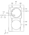
- the interface laser irradiation device 80 has a chuck 100 that holds the polymerized wafer T on the upper surface.
- the chuck 100 attracts and holds a part or the entire surface of the back surface W1b of the first wafer W1.
- the chuck 100 is provided with an elevating pin (not shown) for transferring the polymerized wafer T to and from the transport arm 42.
- the elevating pin is configured to be elevating and lowering by inserting a through hole (not shown) formed through the chuck 100, and supports and elevates the polymerized wafer T from below.
- the chuck 100 is supported by the slider table 102 via the air bearing 101.
- a rotation mechanism 103 is provided on the lower surface side of the slider table 102.
- the rotation mechanism 103 has, for example, a built-in motor as a drive source.
- the chuck 100 is rotatably configured around the ⁇ axis (vertical axis) by the rotation mechanism 103 via the air bearing 101.
- the slider table 102 is configured to be movable along a rail 105 provided on the base 106 and extending in the Y-axis direction by a moving mechanism 104 provided on the lower surface side thereof.
- the drive source of the moving mechanism 104 is not particularly limited, but for example, a linear motor is used.
- a laser irradiation unit 110 is provided above the chuck 100.
- the laser irradiation unit 110 includes a laser head 111, an optical system 112, and a lens 113.
- the laser head 111 oscillates the laser beam in a pulse shape.
- the optical system 112 controls the intensity and position of the laser beam, or attenuates the laser beam to adjust the output.
- the lens 113 is a cylindrical member, and irradiates the polymerized wafer T held by the chuck 100 with laser light.
- the laser light is a pulsed CO 2 laser light
- the laser light emitted from the laser irradiation unit 110 passes through the second wafer W2 and is irradiated to the laser absorption layer P.
- the wavelength of the CO 2 laser light is, for example, 8.9 ⁇ m to 11 ⁇ m.
- the lens 113 is configured to be able to move up and down by an elevating mechanism (not shown).
- a transport pad 120 having a suction surface for sucking and holding the back surface W2b of the second wafer W2 is provided on the lower surface.
- the transport pad 120 is configured to be able to move up and down by an elevating mechanism (not shown).
- the transfer pad 120 transfers the second wafer W2 between the chuck 100 and the transfer arm 42. Specifically, after moving the chuck 100 to the lower side of the transfer pad 120 (the delivery position with the transfer arm 42), the transfer pad 120 is lowered to attract and hold the back surface W2b of the second wafer W2, and then the back surface W2b is sucked and held.
- the transport pad 120 is raised again to peel off from the first wafer W1.
- the peeled second wafer W2 is delivered from the transport pad 120 to the transport arm 42, and is carried out from the interface laser irradiation device 80.
- the transfer pad 120 may be configured to invert the front and back surfaces of the wafer by an inversion mechanism (not shown).
- the wafer processing performed by using the wafer processing system 1 configured as described above will be described.
- a case where the laser lift-off process is performed in the wafer processing system 1, that is, a case where the device layer D2 of the second wafer W2 is transferred to the first wafer W1 will be described.
- the first wafer W1 and the second wafer W2 are bonded to each other in an external bonding device (not shown) of the wafer processing system 1 to form a polymerized wafer T in advance.
- the cassette Ct containing the plurality of polymerized wafers T is placed on the cassette mounting table 10 of the loading / unloading block G1.
- the polymerized wafer T in the cassette Ct is taken out by the wafer transfer device 20.
- the polymerized wafer T taken out from the cassette Ct is transferred to the wafer transfer device 40 via the transition device 30, and then transferred to the interface laser irradiation device 80.
- the second wafer W2 is peeled from the first wafer W1 (laser trim-off processing).
- This processing position is a position where the laser beam can be irradiated from the laser irradiation unit 110 to the polymerized wafer T (laser absorption layer P).
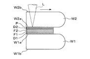
- the laser beam L (CO 2 laser beam) is pulsedly irradiated from the laser irradiation unit 110 toward the back surface W2b of the second wafer W2.
- the laser beam L passes through the second wafer W2 from the back surface W2b side of the second wafer W2 and is absorbed by the laser absorption layer P.
- stress is generated inside the laser absorption layer P that has absorbed the laser light L.
- the stress accumulation layer formed by the irradiation of the laser beam and serving as the base point for peeling of the second wafer W2 (the base point for transfer of the device layer D2) may be referred to as “peeling modified layer M1”. ..
- the laser beam L irradiated to the laser absorption layer P absorbs almost all the energy due to the formation of the peeling modification layer M1 and does not reach the device layer D2. Therefore, it is possible to prevent the device layer D2 from being damaged.
- the laser light L irradiated to the laser absorption layer P is controlled to an output that does not separate the second wafer W2 and the laser absorption layer P by the irradiation of the laser light L.
- the peak power is lowered by increasing the frequency of the laser beam L, and the peeling modified layer is prevented from peeling between the second wafer W2 and the laser absorbing layer P by the irradiation of the laser beam L.
- the peeling modification layer M1 is formed. More specifically, for example, the laser absorption layer P is gasified by irradiation with laser light to eliminate the escape place of the generated gas as described above, so that compressive stress is accumulated as the peeling modification layer M1. Further, for example, heat is generated in the laser absorption layer P due to the absorption of laser light, and the difference in thermal expansion coefficient between the laser absorption layer P and the second wafer W2 or the device layer D2 causes shear stress as the peeling modification layer M1.
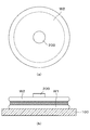
- the rotation mechanism 103 rotates the chuck 100 (polymerized wafer T), and the moving mechanism 104 moves the chuck 100 in the Y-axis direction. Then, the laser beam L is irradiated to the laser absorption layer P from the inside to the outside in the radial direction, and as a result, is spirally irradiated from the inside to the outside.
- the black arrow shown in FIG. 6 indicates the rotation direction of the chuck 100.
- the formation interval of the adjacent peeling and modifying layer M1 in other words, the pulse interval (frequency) of the laser beam L, is peeled off in the adjacent peeling and modifying layer M1 due to the impact generated during the formation of the peeling and modifying layer M1. Is controlled at intervals that do not occur.
- the adjacent peeling and modifying layers M1 are formed so as not to overlap each other in a plan view. Further, at this time, it is preferable that the adjacent peeling and modifying layers M1 are formed in close proximity to each other.
- the laser beam L may be irradiated concentrically in an annular shape.
- the rotation of the chuck 100 and the Y direction of the chuck 100 are alternately performed, it is better to irradiate the laser beam L in a spiral shape as described above to shorten the irradiation time and improve the throughput. Can be done.
- the chuck 100 is rotated when irradiating the laser absorption layer P with the laser beam L, but the lens 113 may be moved to rotate the lens 113 relative to the chuck 100. .. Further, although the chuck 100 is moved in the Y-axis direction, the lens 113 may be moved in the Y-axis direction. Furthermore, the formation direction of the peeling modification layer M1 is not limited to the radial inside to the outside of the laser absorption layer P, and may be formed from the radial outside to the inside.
- non-peeled region R1 The region where M1 is formed (hereinafter, referred to as “non-peeled region R1”) is sequentially formed from the radial inside to the outside of the laser absorption layer P. In the unpeeled region R1, the stress generated in the formation of each peeled modified layer M1 is accumulated as described above.
- the forming position of the peeling reforming layer M1 is near the end of the second wafer W2, in other words, the first wafer.
- the boundary Ad between the bonding region Ac where the W1 and the second wafer W2 are bonded and the unbonded region Ae on the radial outer side of the bonding region Ac is reached.
- the boundary Ad may be, for example, a joint end portion formed by joining the first wafer W1 and the second wafer W2, or for example, the first wafer W1 and the second wafer W2. It may be intentionally formed by removing the bonding interface of the wafer.
- the unbonded region Ae is a region outside the boundary Ad in the radial direction, for example, a region in which the bonding strength between the first wafer W1 and the second wafer W2 is intentionally lost due to removal of the bonding interface or the like. It may be, for example, simply a region outside the radial direction of the bonding region Ac in which the first wafer W1 and the second wafer W2 are actually bonded.
- the formation position of the peeling modified layer M1 reaches the boundary Ad
- the stress accumulated as the peeling modified layer M1 is released to the formation space of the unbonded region Ae, that is, to the outside of the polymerized wafer T.
- the thickness direction of the laser absorbing layer P that is, the laser absorption A force acts in the peeling direction between the layer P and the second wafer W2
- the laser absorbing layer P and the second wafer W2 are peeled off.
- the laser absorption layer P and the second wafer W2 are peeled off in the vicinity of the boundary Ad, the laser absorption layer P and the second wafer W2 are affected by the force acting in the thickness direction of the laser absorption layer P due to the peeling.
- the peeling of the wafer W2 proceeds inward in the radial direction of the laser absorption layer P.
- the peeling that has progressed inward in the radial direction reaches the adjacent peeling modification layer M1. That is, the laser absorption layer P and the second wafer W2 are peeled off at the positions where the adjacent peeling and modifying layers M1 are formed.
- the laser absorption layer P and the second wafer W2 are repeatedly peeled off, the stress is released, and the peeling progresses inward in the radial direction in a chained manner.
- the peeling region R2 is sequentially formed from the radial outer side to the inner side of the laser absorption layer P.
- the entire surface of the second wafer W2 is peeled off from the laser absorption layer P (first wafer W1), so that the device layer D2 of the second wafer W2 is transferred to the first wafer W1 side. ..
- the peak of the laser beam L is prevented so as not to cause peeling of the laser absorbing layer P and the second wafer W2.
- Power (frequency) is controlled.
- the laser absorption layer P and the second wafer W2 are not formed because the peeling modified layer M1 (hereinafter referred to as "starting point modified layer M1s") serving as the starting point of peeling is formed in the vicinity of the boundary Ad.
- starting point modified layer M1s serving as the starting point of peeling
- the chuck 100 is then moved to the delivery position by the moving mechanism 104.
- the transfer pad 120 sucks and holds the back surface W2b of the second wafer W2 as shown in FIG. 9 (a), and then raises the transfer pad 120 as shown in FIG. 9 (b).
- the second wafer W2 is peeled from the laser absorption layer P (first wafer W1).
- the second wafer W2 can be peeled from the laser absorption layer P without applying a large load. can.
- the peeled second wafer W2 is delivered from the transfer pad 120 to the transfer arm 42 of the wafer transfer device 40, and is transferred to the cassette Cw2 of the cassette mounting table 10.
- the surface W2a of the second wafer W2 carried out from the interface laser irradiation device 80 may be cleaned by the cleaning device 60 before being conveyed to the cassette Cw2.
- the first wafer W1 held by the chuck 100 is delivered to the transfer arm 42 of the wafer transfer device 40 via the elevating pin, and is transferred to the cleaning device 60.
- the cleaning device 60 the surface of the laser absorption layer P, which is the peeling surface, is scrubbed.
- the back surface W1b of the first wafer W1 may be cleaned together with the front surface of the laser absorption layer P.
- the first wafer W1 that has undergone all the processing related to the transfer of the device layer D2 to the first wafer W1 is transferred to the cassette Cw1 of the cassette mounting table 10 by the wafer transfer device 20 via the transition device 30. Will be done. In this way, a series of wafer processing in the wafer processing system 1 is completed.
- the output of the laser beam L irradiated by the interface laser irradiation device 80 is controlled to a peak power that does not cause peeling of the laser absorption layer P and the second wafer W2. That is, since it is not necessary to reduce the frequency of the laser beam L when the laser absorption layer P and the second wafer W2 are peeled off, the decrease in the throughput required for the transfer of the device layer D2 to the first wafer W1 is suppressed. Further, even when the peak power of the laser beam L is reduced in this way, the laser absorption layer P and the second wafer are appropriately released by releasing the stress accumulated by the formation of the peeling modification layer M1. W2 peeling can be generated.
- the stress is released by forming the peeling modification layer M1 in the vicinity of the boundary Ad as the starting modification layer M1s, and the laser absorption layer P and the second wafer W2 are peeled in a chained manner.
- the method of starting the peeling is not limited to this.
- the starting point modified layer M1s which is the base point of peeling outside the unpeeled region R1 formed in the laser absorbing layer P
- the laser absorbing layer P and the second wafer W2 are chained. Peeling may be initiated.
- the starting point modification layer M1s is formed with a high peak power (low frequency) at which the laser absorption layer P and the second wafer W2 are peeled off by irradiation with the laser beam L.
- the compressive stress is released, and then the peeling of the laser absorption layer P and the second wafer W2 proceeds in a chain reaction.
- the unpeeled region R1 can be formed by the same method as in the above embodiment. Therefore, it is possible to suppress a decrease in the throughput required for transferring the device layer D2 to the first wafer W1.
- the starting point modified layer M1s can be formed prior to the formation of the unpeeled region R1. That is, the laser absorption layer P and the second wafer W2 are peeled off in advance by forming the starting point modified layer M1s, and then the formation position of the peeling modified layer M1 as the unpeeled region R1 is set to the starting point modified layer M1s. Upon reaching the formation position, the compressive stress is released in the starting point modified layer M1s, and the progress of chain peeling can be started.
- the interval of irradiating the laser beam L that is, the interval of the pulses constant.
- the relative rotation speed of the chuck 100 with respect to the laser irradiation unit 110 is larger than the outer diameter in the radial direction. The inside of the direction is larger.
- the laser beams L may overlap.
- the laser absorption layer P and the second wafer W2 cannot be properly separated from each other at the central portion, or the laser beam L causes missing light, which affects the device layer D2. There is a risk of giving.
- the peeling region R2 naturally extends due to the release of stress.
- the formation of the peeling modification layer M1 may be omitted as long as it is formed. Even when the peeling modification layer M1 is not formed in the central portion of the laser absorption layer P in this way, the peeling is extended by the action of the peeling (stress release) proceeding from the outside in the radial direction, and the laser is also formed in the central portion.
- the absorption layer P and the second wafer W2 can be peeled off.
- the frequency of the laser beam L is reduced on the inner side in the radial direction in which the relative rotation speed of the chuck 100 with respect to the laser irradiation unit 110 (lens 113) is large, and the frequency of the laser light L is on the outer side in the radial direction.
- the relative irradiation interval of the laser beam L to the laser absorption layer P may be controlled to be substantially constant.
- the frequency is changed in this way, if the frequency of the laser beam L is changed in the laser oscillator of the laser head 111, the pulse waveform of the laser beam L also changes. Therefore, complicated adjustment is required in consideration of the output of the laser beam L and the pulse waveform, and it is difficult to control the process of laser processing.
- the frequency of the laser beam L is controlled by using an acousto-optic modulator.
- the laser irradiation unit 110 includes a laser head 111, an optical system 112, and a lens 113.
- the laser head 111 has a laser oscillator 130 that oscillates a laser beam in a pulse shape.
- the frequency of the laser light oscillated from the laser oscillator 130 is the highest frequency that can be controlled by the acousto-optic modulator 131 described later.
- the laser head 111 may have other equipment of the laser oscillator 130, for example, an amplifier.
- the optical system 112 adjusts the output of the laser beam by attenuating the acousto-optic modulator (AOM) 131 as an optical element that diverts the laser beam from the laser oscillator 130 in different directions and the laser beam from the laser oscillator 130. It has an attenuator 132 as an attenuator.
- the acousto-optic modulator 131 and the attenuator 132 are provided in this order from the laser oscillator 130 side.
- the acousto-optic modulator 131 is an optical modulator that electrically controls the intensity and position of laser light at high speed. As shown in FIG. 12, the acousto-optic modulator 131 directs the laser beam L1 in different directions by applying a voltage to change the refractive index of the laser beam L1 when the laser beam L1 from the laser oscillator 130 is incident. Convert to. Specifically, the change angle of the laser beam L1 can be controlled by adjusting the voltage. In the present embodiment, for example, the laser light L1 is redirected in two different directions, the laser light L2 in one direction is irradiated to the laser absorption layer P, and the laser light L3 in the other direction is not irradiated to the laser absorption layer P. By controlling the conversion of the laser beams L2 and L3, the frequency of the laser beam L2 irradiated on the laser absorption layer P can be adjusted.
- the frequency of the laser beam L2 irradiated to the laser absorption layer P can be adjusted by thinning out the pulse of the laser beam L1 using the acousto-optic modulator 131. For example, if the conversion ratio of the laser light L2 and the laser light L3 with respect to the laser light L1 is set to 100: 0 at a certain timing, the laser light L1 becomes the laser light L2 as it is and is irradiated to the laser absorption layer P.
- the frequency of the laser beam L2 converted by the acousto-optic modulator 131 shown in FIG. 13 (b) can be adjusted with respect to the frequency of the laser beam L1 from the laser oscillator 130 shown in FIG. 13 (a). can.
- the frequency of the laser beam L1 is the highest frequency that can be controlled by the acousto-optic modulator 131, the frequency of the laser beam L2 can be arbitrarily adjusted.
- the horizontal axis of FIG. 13 indicates time, and the vertical axis indicates the intensity of the laser beam L2. That is, the density in the graph of FIG. 13 indicates the frequency of the laser beam L2.
- the frequency of the laser light L1 oscillated from the laser oscillator 130 is not changed, the pulse waveform of the laser light L1 does not change, and the pulse waveform of the laser light L2 can be the same as the pulse waveform of the laser light L1. Therefore, the frequency of the laser beam L2 can be easily adjusted, the conventional complicated adjustment as described above becomes unnecessary, and the process control of the laser processing becomes easy.
- the acousto-optic modulator 131 is used as the optical element, but the present invention is not limited to this.
- an electro-optical modulator (EOM) may be used as the optical element.
- an optical deflector such as an acoustic optical deflector (AOD) or an electro-optical deflector (EOD) may be used.
- the energy required for peeling is set to 400 ⁇ J on each of the radial outer side and inner side of the laser absorption layer P.
- the required frequency of the laser beam L2 on the radial outer side of the laser absorption layer P is 100 kHz, and the required frequency of the laser beam on the inner side is 50 kHz.
- the frequency of the laser beam L1 from the laser oscillator 130 is 100 kHz, and the output is 40 W.
- the pulse of the laser beam L1 from the laser oscillator 130 is not thinned out in the acousto-optic modulator 131 with respect to the radial outside of the laser absorption layer P.
- the frequency of the laser beam L2 irradiated on the laser absorption layer P can be set to 100 kHz, which is the same as the frequency of the laser beam L1.
- the output of the laser beam L2 is 40 W, which is the same as the output of the laser beam L1.
- the pulse of the laser beam L1 from the laser oscillator 130 is drawn for half a minute in the acousto-optic modulator 131 toward the radial inside of the laser absorption layer P.
- the frequency of the laser beam L2 irradiated on the laser absorption layer P can be set to 50 kHz, which is half the frequency of the laser beam L1.
- the output of the laser light L2 becomes 20 W, which is half of the output of the laser light L1.
- the rotation speed of the chuck 100 is controlled so that the pulse interval becomes constant according to the frequency of the laser beam L2 and the irradiation position. Then, at the central portion of the laser absorption layer P, the maximum rotation speed of the chuck 100 is maintained, and the acousto-optic modulator 131 adjusts the frequency of the laser beam L2 in accordance with the maximum rotation speed.
- laser processing can be performed while maintaining the high rotation speed of the chuck 100 and the high frequency of the laser beam L2 to the maximum, and high-throughput laser processing can be realized.
- the frequency of the laser light L1 from the laser oscillator 130 is not changed, the pulse waveform of the laser light L1 does not change, and the pulse waveform of the laser light L2 can be the same as the pulse waveform of the laser light L1. Therefore, the frequency of the laser beam L2 can be easily adjusted, and continuous seamless processing becomes possible. As a result, the process control of the laser processing becomes easy, and a stable process can be realized.
- the output of the laser beam L1 from the laser oscillator 130 was 40 W, it was not necessary to adjust the output for the energy of 400 ⁇ J required for peeling.
- the output of the laser beam L1 may be attenuated by 20% in the attenuator 132 to adjust the output.
- the acousto-optic modulator 131 is provided on the upstream side of the attenuator 132 inside the optical system 112, but the installation location is not limited to this.
- the acousto-optic modulator 131 may be provided inside the optical system 112 on the downstream side of the attenuator 132.
- the acousto-optic modulator 131 may be provided inside the laser head 111 on the downstream side of the laser oscillator 130.
- the acousto-optic modulator 131 may be provided at two or more locations at the above installation positions.
- the output can be finely adjusted with the attenuator 132.
- the output of the laser beam L1 oscillated from the laser oscillator 130 may vary depending on the individual difference of the laser oscillator 130. In the attenuator 132, such output variation can be adjusted. Further, when the output of the laser beam L1 from the laser oscillator 130 is monitored over time, the attenuator 132 can be feedback-controlled to adjust the output. From the viewpoint of finely adjusting the output of the laser beam L2 with the attenuator 132, the acousto-optic modulator 131 is preferably provided on the upstream side of the attenuator 132 as shown in FIG.
- the attenuator 132 may be omitted in the laser irradiation unit 110 of the above embodiment.
- the output of the laser beam L2 can be adjusted by the acousto-optic modulator 131 instead of the attenuator 132.
- the conversion rate of the laser light L2 and the laser light L3 with respect to the laser light L1 is determined in the acoustic optical modulator 131. If it is set to 80:20, the output of the laser beam L2 can be set to 40 W.
- the peeling and modifying layer M1 in which the bonding strength between the second wafer W2 and the laser absorbing layer P is reduced is formed on the laser absorbing layer P, and the peeling and modifying layer M1 is used as a base point for the second peeling and modifying layer M1.
- Wafer W2 and laser absorption layer P were peeled off.
- a region in which the laser beam is not irradiated in the plane of the laser absorption layer P and the bonding strength is not lowered hereinafter, referred to as “unformed region R3”) is formed. If this happens, the second wafer W2 and the laser absorption layer P may not be properly peeled off.
- a part (silicon piece) of the second wafer W2 is formed on the surface of the laser absorption layer P after peeling. May remain.
- the peeling modified layer M1 non-peeling region R1 so as to reduce the formation area of the unformed region R3 in the plane of the laser absorption layer P.
- the laser irradiation type for the laser absorption layer P may be controlled to reduce the unformed region R3. That is, the laser irradiation type may be, for example, a quadrangle.
- the region in which the bonding strength with the second wafer W2 is reduced in the plane of the laser absorption layer P increases, and as a result, the laser absorption layer P increases. And the second wafer W2 can be appropriately peeled off.
- the laser absorption layer P, the device layer D2, and the surface film F2 are laminated in this order on the surface W2a of the second wafer W2, but the second wafer W2 and the laser absorption layer P As shown in FIG. 18A, a peeling promoting layer P2 may be further formed between them.
- the peeling promoting layer P2 has transparency to laser light (CO 2 laser), and the adhesion to the second wafer W2 (silicon) is at least the adhesion to the laser absorbing layer P (SiO 2 ). Smaller ones, such as silicon nitride (SiN), are selected.
- the laser beam L (CO 2 laser) is directed toward the back surface W2b of the second wafer W2.
- Light is irradiated in a pulse shape.
- the laser beam L passes through the second wafer W2 and the peeling promoting layer P2 from the back surface W2b side of the second wafer W2 and is absorbed by the laser absorbing layer P.
- the peeling modification layer M1 is formed inside the laser absorbing layer P that has absorbed the laser light L.
- the stress generated by the irradiation of the laser beam L usually stays at the irradiation position of the laser beam L (inside the laser absorption layer) as shown in the above embodiment to form the peeling modification layer M1.
- the peeling promoting layer P2 is formed as in the present embodiment, the adhesion between the peeling promoting layer P2 and the second wafer W2 is smaller than the adhesion between the peeling promoting layer P2 and the laser absorbing layer P. Therefore, as shown in FIG. 18C, the generated stress permeates the peeling promoting layer P2 and is accumulated at the interface between the peeling promoting layer P2 and the second wafer W2.
- the stress generated by irradiating the laser beam L moves and accumulates at the interface between the peeling promoting layer P2 and the second wafer W2, which can stay more stably, thereby causing the peeling promoting layer.
- the bonding strength between P2 and the second wafer W2 is reduced.
- the peeling promoting layer P2 and the second wafer W2 can be appropriately peeled after that. Further, at this time, since the adhesion between the peeling promoting layer P2 and the second wafer W2 is low, a part of the second wafer W2 may remain on the surface of the peeling promoting layer P2 after peeling as shown in FIG. , Appropriately suppressed. Furthermore, in the present embodiment, since the laser beam L is absorbed by the laser absorbing layer P, the exposed surface after peeling, that is, the surface W2a of the second wafer W2 and the surface of the peeling promoting layer P2 are damaged. Remaining is more appropriately suppressed.
- the film thickness of the peeling promoting layer P2 is thinner than that of the laser absorbing layer P. It is preferably about 1/10 of the film thickness.
- the second wafer W2 is the laser absorbing layer via the peeling promoting layer P2. Since it is peeled from P, a part of the second wafer W2 does not remain on the surface of the laser absorption layer P after peeling as shown in FIG. That is, this can protect the surface W2a of the second wafer W2 and suppress the roughness of the peeled surface.
- the peeling promoting layer P2 used has low adhesion to the second wafer W2 (silicon), but the peeling promoting layer P2 is not limited to this, for example, the second wafer.
- Wafer W2 (silicon) and a wafer having a coefficient of thermal expansion different from that of the wafer W2 (silicon) may be used.
- the amount of deformation due to heat generated by irradiation of the laser absorption layer P with the laser beam L differs between the second wafer W2 and the peeling promotion layer P2, whereby the interface between the second wafer W2 and the peeling promotion layer P2 A shearing force is generated, and the second wafer W2 and the peeling promoting layer P2 can be peeled off.
- the peeling of the second wafer W2 and the peeling promoting layer P2 is promoted by releasing the compressive stress generated by the irradiation of the laser beam and accumulated as the peeling reforming layer M1.
- the stress generated in this way may cause the laminated wafer T to warp.
- the polymerized wafer T may be pressed from above when the laser absorption layer P is irradiated with the laser beam L.
- the central portion of the polymerized wafer T may be pressed by the pressing member 200 as shown in FIG.
- a laser irradiation process that is, an unpeeled region R1 is formed in advance in the central portion of the laser absorption layer P, which is the pressing range by the pressing member 200.
- the unpeeled region R1 is then pressed by the pressing member 200.
- the unpeeled region R1 may be formed from the outer side in the radial direction to the inner side. That is, first, the unpeeled region R1 is formed from the outer peripheral portion to the central portion of the laser absorption layer P. At this time, the outer peripheral side end portion, which is the formation start position of the unpeeled region R1, is determined slightly radially inward from the outer peripheral side end portion of the laser absorption layer P, and the stress is not released. After forming the unpeeled region R1, the unpeeled region R1 is then pressed by the pressing member 200. After that, with the unpeeled region R1 pressed by the pressing member 200, the formation position of the unpeeled region R1 reaches the outer peripheral end of the laser absorption layer P.
- chain peeling is started by forming the starting point modifying layer M1s on the radial outer side of the second wafer W2. At this time, since the central portion of the polymerized wafer T is suppressed by the pressing member 200, warpage of the polymerized wafer T is suppressed.
- the end portion of the pressing member 200 is configured to be rotatable together with the polymerized wafer T.
- the peripheral edge portion We of the polymerized wafer T may be pressed by the pressing member 200 as shown in FIG.
- a laser irradiation process that is, a peeling region R2 is formed in advance on the outer peripheral portion of the laser absorption layer P, which is the pressing range by the pressing member 200. After forming the peeling region R2, the peeling region R2 is then pressed by the pressing member 200.
- the unpeeled region R1 is started from the inside to the outside in the radial direction at the central portion of the laser absorption layer P. Then, when the formed region of the unpeeled region R1 reaches the peeled region R2, the chain peeling of the second wafer W2 is started. At this time, since the outer peripheral portion of the polymerized wafer T is suppressed by the pressing member 200, warpage of the polymerized wafer T is suppressed.
- a reflective film R may be provided between the laser absorption layer P and the device layer D2 as shown in FIG. That is, the reflective film R is formed on the surface of the laser absorbing layer P opposite to the incident surface of the laser beam L.
- a material having a high reflectance to the laser beam L and a high melting point for example, a metal film is used.
- the device layer D2 is a layer having a function and is different from the reflective film R.
- the laser light L emitted from the laser irradiation unit 110 passes through the second wafer W2 and is almost completely absorbed by the laser absorption layer P, but even if there is a laser light L that cannot be completely absorbed. , Reflected by the reflective film R. As a result, the laser beam L does not reach the device layer D2, and it is possible to reliably suppress the device layer D2 from being damaged.
- the laser light L reflected by the reflective film R is absorbed by the laser absorbing layer P. Therefore, the peeling efficiency of the second wafer W2 can be improved.
- the wafer processing system 1 performs the laser lift-off processing of the polymerized wafer T, that is, the transfer processing of the device layer D2 on the first wafer W1, has been described.
- the wafer processing system In No. 1 the edge trim processing of the second wafer W2 can be performed.
- the edge trim of the second wafer W2 is performed in the wafer processing system 1 will be described.
- the polymerized wafer T is taken out by the wafer transfer device 20 from the cassette Ct placed on the cassette mounting table 10 of the carry-in / out block G1, and is delivered to the wafer transfer device 40 via the transition device 30, and then for internal use. It is conveyed to the laser irradiation device 70.
- the inside of the second wafer W2 is irradiated with the laser light L2 (YAG laser light), and the peripheral portion We is removed in the edge trim described later.
- a peripheral modification layer M2 serving as a base point is formed. Cracks C2 extend from the peripheral modified layer M2 in the thickness direction of the second wafer W2. The upper end portion and the lower end portion of the crack C2 reach, for example, the back surface W2b and the front surface W2a of the second wafer W2, respectively.
- the polymerized wafer T in which the peripheral modification layer M2 is formed inside the second wafer W2 is then transferred by the wafer transfer device 40 to the interface laser irradiation device 80.
- the bonding strength between the laser absorbing layer P and the second wafer W2 at the peripheral edge portion We as the removal target of the second wafer W2 is lowered.
- the laser absorption layer P is irradiated with the laser beam L (CO 2 laser)
- the peripheral modification layer M2 formed by the internal laser irradiation device 70 is more radial than the peripheral modification layer M2.
- a peeling modified layer M1 (non-peeling region R1) is formed on the outside.
- the chuck 100 (polymerized wafer T) is rotated by the rotation mechanism 103, and the chuck 100 is moved in the Y-axis direction by the moving mechanism 104. Then, the laser beam L is irradiated to the laser absorption layer P from the inside to the outside in the radial direction, and as a result, is spirally irradiated from the inside to the outside.
- the polymerized wafer T for which the laser absorption layer P and the second wafer W2 on the peripheral edge We have been peeled off is then conveyed to the peripheral edge removing device 50 by the wafer transfer device 40.
- the peripheral edge portion We of the second wafer W2 is removed (edge trim) from the peripheral edge modifying layer M2 and the crack C2 as the base points of the polymerized wafer T. ..
- the edge trimming method in the peripheral edge removing device 50 can be arbitrarily selected. At this time, when the peripheral portion We are removed, the bonding strength between the second wafer W2 and the laser absorption layer P is lowered due to the formation of the peeling modification layer M1, so that the peripheral portion We can be easily removed. ..
- the polymerized wafer T from which the peripheral portion We of the second wafer W2 has been removed is then transferred to the cleaning device 60 by the wafer transfer device 40.
- the cleaning device 60 scrubbing of the polymerized wafer T is performed.
- the polymerized wafer T that has been subjected to all the processing is carried out from the cleaning device 60 by the wafer transfer device 40, and is transferred to the cassette Ct of the cassette mounting table 10 by the wafer transfer device 20 via the transition device 30. In this way, a series of wafer processing in the wafer processing system 1 is completed.
- the technique according to the present disclosure it is possible to reduce the bonding strength between the second wafer W2 and the laser absorption layer P at the peripheral edge portion We in the interface laser irradiation device 80, thereby removing the peripheral edge.
- the peripheral portion We can be appropriately removed, that is, edge trimming can be performed.
- the processing order of the polymerized wafer T by the internal laser irradiation device 70 and the interface laser irradiation device 80 is not limited to the above embodiment, and the peripheral portion We is peeled off in the interface laser irradiation device 80. After that, the peripheral modification layer M2 may be formed in the internal laser irradiation device 70.
- D2 Device layer L Laser light M1 Detachment modification layer M1s Origin modification layer P Laser absorption layer T Polymerized wafer W1 First wafer W2 Second wafer W2a Front surface W2b Back surface
Landscapes
- Engineering & Computer Science (AREA)
- Physics & Mathematics (AREA)
- Microelectronics & Electronic Packaging (AREA)
- General Physics & Mathematics (AREA)
- Manufacturing & Machinery (AREA)
- Computer Hardware Design (AREA)
- Power Engineering (AREA)
- Condensed Matter Physics & Semiconductors (AREA)
- Optics & Photonics (AREA)
- Toxicology (AREA)
- Health & Medical Sciences (AREA)
- High Energy & Nuclear Physics (AREA)
- Mechanical Engineering (AREA)
- Plasma & Fusion (AREA)
- Electromagnetism (AREA)
- Oil, Petroleum & Natural Gas (AREA)
- General Chemical & Material Sciences (AREA)
- Chemical Kinetics & Catalysis (AREA)
- Chemical & Material Sciences (AREA)
- Laser Beam Processing (AREA)
- Element Separation (AREA)
- Drying Of Semiconductors (AREA)
Abstract
Description
L レーザ光
M1 剥離改質層
M1s 起点改質層
P レーザ吸収層
T 重合ウェハ
W1 第1のウェハ
W2 第2のウェハ
W2a 表面
W2b 裏面
Claims (26)
- 第1の基板と第2の基板が接合された重合基板の処理方法であって、
前記第2の基板にはレーザ吸収層が形成され、
前記レーザ吸収層に対して、レーザ光をパルス状に照射して剥離改質層を形成し、前記レーザ吸収層の内部に応力を蓄積することと、
蓄積された前記応力を連鎖的に解放し、前記第2の基板を剥離することと、を含む、基板処理方法。 - 前記剥離改質層の形成時においては前記レーザ吸収層と前記第2の基板の剥離を発生させない、請求項1に記載の基板処理方法。
- 前記応力の連鎖的な解放の起点となる起点改質層を形成することを含む、請求項1または2に記載の基板処理方法。
- 前記起点改質層は、前記第1の基板と前記第2の基板が接合された接合領域の端部において前記レーザ吸収層の内部に形成され、
前記起点改質層の形成時においては、当該起点改質層の形成により生じる応力を、前記接合領域の径方向側の領域である未接合領域に解放することで、前記レーザ吸収層と前記第2の基板に剥離を発生させ、
前記連鎖的な応力の解放は、前記剥離改質層の形成により蓄積された前記応力を、前記起点改質層の形成による剥離領域に解放することで開始する、請求項3に記載の基板処理方法。 - 起点改質層の形成時においては、レーザ光の照射により前記レーザ吸収層と前記第2の基板の剥離を発生させ、
前記連鎖的な応力の解放は、前記剥離改質層の形成により蓄積された前記応力を、前記起点改質層の形成による剥離領域に解放することで開始する、請求項1~3のいずれか一項に記載の基板処理方法。 - 前記起点改質層を、前記剥離改質層よりも径方向外側に形成する、請求項4または5に記載の基板処理方法。
- 前記第2の基板の除去対象の周縁部と、前記第2の基板の中央部の境界に沿って周縁改質層を形成することを含み、
前記剥離改質層を、前記周縁改質層よりも径方向外側に形成する、請求項1~6のいずれか一項に記載の基板処理方法。 - 前記剥離改質層を前記レーザ吸収層の中心部においては形成しない、請求項1~7のいずれか一項に記載の基板処理方法。
- 前記剥離改質層の形成位置、及び/又は、前記剥離改質層の形成時における前記レーザ光の照射形を制御することにより、前記レーザ吸収層に対する前記剥離改質層の形成面積を増加させる、請求項1~8のいずれか一項に記載の基板処理方法。
- 前記第2の基板と前記レーザ吸収層の間には前記第2の基板の剥離を促進する剥離促進層が更に形成されている、請求項1~9のいずれか一項に記載の基板処理方法。
- 前記レーザ吸収層に前記レーザ光を照射する際、レーザ発振器から光学素子に向けてパルス状のレーザ光を発振し、前記光学素子においてレーザ光の周波数を調整する、請求項1~10のいずれか一項に記載の基板処理方法。
- 前記レーザ発振器からのレーザ光の周波数は、前記光学素子が制御できる最高周波数である、請求項11に記載の基板処理方法。
- 前記レーザ吸収層に前記レーザ光を照射する際、減衰器において前記レーザ発振器からのレーザ光を減衰させる、請求項11又は12に記載の基板処理方法。
- 第1の基板と第2の基板が接合された重合基板を処理する装置であって、
前記第2の基板にはレーザ吸収層が形成され、
前記第2の基板の前記レーザ吸収層に対してレーザ光をパルス状に照射するレーザ照射部と、
前記レーザ照射部の動作を制御する制御部と、を有し、
前記制御部は、
前記レーザ光の照射により剥離改質層を形成して前記レーザ吸収層の内部に応力を蓄積した後、
蓄積された前記応力の連鎖的な解放により前記第2の基板を剥離するように、前記レーザ照射部の動作を制御する、基板処理装置。 - 前記制御部は、前記剥離改質層の形成時においては前記レーザ吸収層と前記第2の基板の剥離を発生させないように、前記レーザ光の出力を制御する、請求項14に記載の基板処理装置。
- 前記制御部は、前記応力の連鎖的な解放の起点となる起点改質層を形成するように、前記レーザ照射部の動作を制御する、請求項14または15に記載の基板処理装置。
- 前記制御部は、
前記起点改質層を、前記第1の基板と前記第2の基板が接合された接合領域の端部において前記レーザ吸収層の内部に形成し、
当該起点改質層の形成時においては、当該起点改質層の形成により生じる応力を、前記接合領域の径方向側の領域である未接合領域に解放することで、前記レーザ吸収層と前記第2の基板に剥離を発生させ、
前記連鎖的な応力の解放を、前記剥離改質層の形成により蓄積された前記応力を、前記起点改質層の形成による剥離領域に解放することで開始するように、前記レーザ照射部の動作を制御する、請求項16に記載の基板処理装置。 - 前記制御部は、
前記起点改質層の形成時においては、レーザ光の照射により前記レーザ吸収層と前記第2の基板の剥離が発生するように、前記レーザ光の出力を制御するとともに、
前記連鎖的な応力の解放を、前記剥離改質層の形成により蓄積された前記応力を、前記起点改質層の形成による剥離領域に解放することで開始するように、前記レーザ照射部の動作を制御する、請求項16に記載の基板処理装置。 - 前記制御部は、
前記起点改質層を、前記剥離改質層よりも径方向外側に形成するように、前記レーザ照射部の動作を制御する請求項17または18に記載の基板処理装置。 - 前記第2の基板の除去対象の周縁部と、前記第2の基板の中央部の境界に沿って周縁改質層を形成する第2のレーザ照射部を有し、
前記制御部は、前記剥離改質層を、前記周縁改質層よりも径方向外側に形成するように、前記レーザ照射部の動作を制御する請求項14~19のいずれか一項に記載の基板処理装置。 - 前記制御部は、前記剥離改質層を前記レーザ吸収層の中心部においては形成しないように、前記レーザ照射部の動作を制御する、請求項14~20のいずれか一項に記載の基板処理装置。
- 前記制御部は、前記レーザ吸収層に対する前記剥離改質層の形成面積を増加させるように、前記剥離改質層の形成位置、及び/又は、前記剥離改質層の形成時における前記レーザ光の照射形を制御する、請求項14~21のいずれか一項に記載の基板処理装置。
- 前記第2の基板と前記レーザ吸収層の間には前記第2の基板の剥離を促進する剥離促進層が更に形成されている、請求項14~22のいずれか一項に記載の基板処理装置。
- 前記レーザ照射部を制御する制御部を有し、
前記レーザ照射部は、
レーザ光をパルス状に発振するレーザ発振器と、
前記レーザ発振器からのレーザ光を異なる方向に変向させる光学素子と、を有し、
前記制御部は、前記光学素子を制御して、前記レーザ吸収層に照射されるレーザ光の周波数を調整する、請求項14~23のいずれか一項に記載の基板処理装置。 - 前記レーザ発振器からのレーザ光の周波数は、前記変向が制御できる最高周波数である、請求項24に記載の基板処理装置。
- 前記レーザ照射部は、前記レーザ発振器からのレーザ光を減衰させる減衰器を有する、請求項24又は25に記載の基板処理装置。
Priority Applications (4)
| Application Number | Priority Date | Filing Date | Title |
|---|---|---|---|
| JP2022509458A JPWO2021192854A1 (ja) | 2020-03-24 | 2021-03-02 | |
| CN202180021036.6A CN115335965A (zh) | 2020-03-24 | 2021-03-02 | 基板处理方法和基板处理装置 |
| KR1020227036631A KR20220158024A (ko) | 2020-03-24 | 2021-03-02 | 기판 처리 방법 및 기판 처리 장치 |
| US17/907,217 US20240087900A1 (en) | 2020-03-24 | 2021-03-02 | Substrate processing method and substrate processing apparatus |
Applications Claiming Priority (2)
| Application Number | Priority Date | Filing Date | Title |
|---|---|---|---|
| JP2020-053183 | 2020-03-24 | ||
| JP2020053183 | 2020-03-24 |
Publications (1)
| Publication Number | Publication Date |
|---|---|
| WO2021192854A1 true WO2021192854A1 (ja) | 2021-09-30 |
Family
ID=77892476
Family Applications (1)
| Application Number | Title | Priority Date | Filing Date |
|---|---|---|---|
| PCT/JP2021/007940 WO2021192854A1 (ja) | 2020-03-24 | 2021-03-02 | 基板処理方法及び基板処理装置 |
Country Status (6)
| Country | Link |
|---|---|
| US (1) | US20240087900A1 (ja) |
| JP (1) | JPWO2021192854A1 (ja) |
| KR (1) | KR20220158024A (ja) |
| CN (1) | CN115335965A (ja) |
| TW (1) | TW202205398A (ja) |
| WO (1) | WO2021192854A1 (ja) |
Cited By (2)
| Publication number | Priority date | Publication date | Assignee | Title |
|---|---|---|---|---|
| WO2024024191A1 (ja) * | 2022-07-27 | 2024-02-01 | 東京エレクトロン株式会社 | 基板処理システム、基板処理方法及びデバイス構造 |
| WO2024034197A1 (ja) * | 2022-08-09 | 2024-02-15 | 東京エレクトロン株式会社 | 基板処理装置及び基板処理方法 |
Citations (7)
| Publication number | Priority date | Publication date | Assignee | Title |
|---|---|---|---|---|
| JPH10125929A (ja) * | 1996-08-27 | 1998-05-15 | Seiko Epson Corp | 剥離方法 |
| JP2007165848A (ja) * | 2005-11-16 | 2007-06-28 | Denso Corp | 半導体チップの製造方法 |
| JP2008503877A (ja) * | 2004-06-18 | 2008-02-07 | エレクトロ サイエンティフィック インダストリーズ インコーポレーテッド | 複数のレーザビームスポットを使用する半導体構造加工 |
| JP2018117060A (ja) * | 2017-01-19 | 2018-07-26 | 株式会社ブイ・テクノロジー | 剥離基板及びレーザリフトオフ方法 |
| JP2018207009A (ja) * | 2017-06-07 | 2018-12-27 | 株式会社ディスコ | 被加工物の加工方法 |
| WO2019208298A1 (ja) * | 2018-04-27 | 2019-10-31 | 東京エレクトロン株式会社 | 基板処理システム及び基板処理方法 |
| WO2020017599A1 (ja) * | 2018-07-19 | 2020-01-23 | 東京エレクトロン株式会社 | 基板処理システム及び基板処理方法 |
Family Cites Families (1)
| Publication number | Priority date | Publication date | Assignee | Title |
|---|---|---|---|---|
| JP2007220749A (ja) | 2006-02-14 | 2007-08-30 | Seiko Epson Corp | 半導体装置の製造方法 |
-
2021
- 2021-03-02 JP JP2022509458A patent/JPWO2021192854A1/ja active Pending
- 2021-03-02 US US17/907,217 patent/US20240087900A1/en active Pending
- 2021-03-02 CN CN202180021036.6A patent/CN115335965A/zh active Pending
- 2021-03-02 KR KR1020227036631A patent/KR20220158024A/ko active Search and Examination
- 2021-03-02 WO PCT/JP2021/007940 patent/WO2021192854A1/ja active Application Filing
- 2021-03-03 TW TW110107474A patent/TW202205398A/zh unknown
Patent Citations (7)
| Publication number | Priority date | Publication date | Assignee | Title |
|---|---|---|---|---|
| JPH10125929A (ja) * | 1996-08-27 | 1998-05-15 | Seiko Epson Corp | 剥離方法 |
| JP2008503877A (ja) * | 2004-06-18 | 2008-02-07 | エレクトロ サイエンティフィック インダストリーズ インコーポレーテッド | 複数のレーザビームスポットを使用する半導体構造加工 |
| JP2007165848A (ja) * | 2005-11-16 | 2007-06-28 | Denso Corp | 半導体チップの製造方法 |
| JP2018117060A (ja) * | 2017-01-19 | 2018-07-26 | 株式会社ブイ・テクノロジー | 剥離基板及びレーザリフトオフ方法 |
| JP2018207009A (ja) * | 2017-06-07 | 2018-12-27 | 株式会社ディスコ | 被加工物の加工方法 |
| WO2019208298A1 (ja) * | 2018-04-27 | 2019-10-31 | 東京エレクトロン株式会社 | 基板処理システム及び基板処理方法 |
| WO2020017599A1 (ja) * | 2018-07-19 | 2020-01-23 | 東京エレクトロン株式会社 | 基板処理システム及び基板処理方法 |
Cited By (2)
| Publication number | Priority date | Publication date | Assignee | Title |
|---|---|---|---|---|
| WO2024024191A1 (ja) * | 2022-07-27 | 2024-02-01 | 東京エレクトロン株式会社 | 基板処理システム、基板処理方法及びデバイス構造 |
| WO2024034197A1 (ja) * | 2022-08-09 | 2024-02-15 | 東京エレクトロン株式会社 | 基板処理装置及び基板処理方法 |
Also Published As
| Publication number | Publication date |
|---|---|
| US20240087900A1 (en) | 2024-03-14 |
| KR20220158024A (ko) | 2022-11-29 |
| TW202205398A (zh) | 2022-02-01 |
| CN115335965A (zh) | 2022-11-11 |
| JPWO2021192854A1 (ja) | 2021-09-30 |
Similar Documents
| Publication | Publication Date | Title |
|---|---|---|
| WO2021192853A1 (ja) | 基板処理方法及び基板処理装置 | |
| JP7304433B2 (ja) | 基板処理方法及び基板処理装置 | |
| JP5766530B2 (ja) | 光デバイスウエーハの加工方法 | |
| JP7149393B2 (ja) | 基板処理システム及び基板処理方法 | |
| WO2021192854A1 (ja) | 基板処理方法及び基板処理装置 | |
| JP7386077B2 (ja) | 基板処理装置及び基板処理方法 | |
| JP2006156456A (ja) | フィルム剥離方法およびフィルム剥離装置 | |
| WO2020213478A1 (ja) | 処理装置及び処理方法 | |
| TW202314842A (zh) | 處理方法及處理系統 | |
| WO2024034197A1 (ja) | 基板処理装置及び基板処理方法 | |
| WO2024024191A1 (ja) | 基板処理システム、基板処理方法及びデバイス構造 | |
| JP7308292B2 (ja) | 基板処理装置及び基板処理方法 | |
| JP2022091504A (ja) | レーザ照射システム、基板処理装置及び基板処理方法 | |
| JP2021068869A (ja) | 基板処理方法及び基板処理システム | |
| JP7354420B2 (ja) | 基板処理方法及び基板処理装置 | |
| WO2022153886A1 (ja) | 基板処理装置、基板処理方法及び基板製造方法 | |
| US20240128086A1 (en) | Method of processing wafer | |
| WO2022153894A1 (ja) | 基板処理装置及び基板処理方法 | |
| WO2022153895A1 (ja) | 基板処理装置及び基板処理方法 | |
| WO2021084934A1 (ja) | 基板処理方法及び基板処理システム | |
| JP2021012950A (ja) | 支持体剥離方法及び支持体剥離システム | |
| JP2019009274A (ja) | ウェーハの加工方法 |
Legal Events
| Date | Code | Title | Description |
|---|---|---|---|
| 121 | Ep: the epo has been informed by wipo that ep was designated in this application |
Ref document number: 21776227 Country of ref document: EP Kind code of ref document: A1 |
|
| ENP | Entry into the national phase |
Ref document number: 2022509458 Country of ref document: JP Kind code of ref document: A |
|
| ENP | Entry into the national phase |
Ref document number: 20227036631 Country of ref document: KR Kind code of ref document: A |
|
| NENP | Non-entry into the national phase |
Ref country code: DE |
|
| 122 | Ep: pct application non-entry in european phase |
Ref document number: 21776227 Country of ref document: EP Kind code of ref document: A1 |