WO2021187535A1 - 光電気伝送複合モジュール - Google Patents
光電気伝送複合モジュール Download PDFInfo
- Publication number
- WO2021187535A1 WO2021187535A1 PCT/JP2021/010881 JP2021010881W WO2021187535A1 WO 2021187535 A1 WO2021187535 A1 WO 2021187535A1 JP 2021010881 W JP2021010881 W JP 2021010881W WO 2021187535 A1 WO2021187535 A1 WO 2021187535A1
- Authority
- WO
- WIPO (PCT)
- Prior art keywords
- heat radiating
- wall
- layer
- photoelectric conversion
- thickness direction
- Prior art date
- Legal status (The legal status is an assumption and is not a legal conclusion. Google has not performed a legal analysis and makes no representation as to the accuracy of the status listed.)
- Ceased
Links
Images


Classifications
-
- H—ELECTRICITY
- H05—ELECTRIC TECHNIQUES NOT OTHERWISE PROVIDED FOR
- H05K—PRINTED CIRCUITS; CASINGS OR CONSTRUCTIONAL DETAILS OF ELECTRIC APPARATUS; MANUFACTURE OF ASSEMBLAGES OF ELECTRICAL COMPONENTS
- H05K7/00—Constructional details common to different types of electric apparatus
- H05K7/20—Modifications to facilitate cooling, ventilating, or heating
- H05K7/2039—Modifications to facilitate cooling, ventilating, or heating characterised by the heat transfer by conduction from the heat generating element to a dissipating body
-
- G—PHYSICS
- G02—OPTICS
- G02B—OPTICAL ELEMENTS, SYSTEMS OR APPARATUS
- G02B6/00—Light guides; Structural details of arrangements comprising light guides and other optical elements, e.g. couplings
- G02B6/24—Coupling light guides
- G02B6/42—Coupling light guides with opto-electronic elements
- G02B6/4201—Packages, e.g. shape, construction, internal or external details
- G02B6/4266—Thermal aspects, temperature control or temperature monitoring
- G02B6/4268—Cooling
- G02B6/4269—Cooling with heat sinks or radiation fins
-
- G—PHYSICS
- G02—OPTICS
- G02B—OPTICAL ELEMENTS, SYSTEMS OR APPARATUS
- G02B6/00—Light guides; Structural details of arrangements comprising light guides and other optical elements, e.g. couplings
- G02B6/24—Coupling light guides
- G02B6/42—Coupling light guides with opto-electronic elements
-
- G—PHYSICS
- G02—OPTICS
- G02B—OPTICAL ELEMENTS, SYSTEMS OR APPARATUS
- G02B6/00—Light guides; Structural details of arrangements comprising light guides and other optical elements, e.g. couplings
- G02B6/10—Light guides; Structural details of arrangements comprising light guides and other optical elements, e.g. couplings of the optical waveguide type
- G02B6/12—Light guides; Structural details of arrangements comprising light guides and other optical elements, e.g. couplings of the optical waveguide type of the integrated circuit kind
-
- G—PHYSICS
- G02—OPTICS
- G02B—OPTICAL ELEMENTS, SYSTEMS OR APPARATUS
- G02B6/00—Light guides; Structural details of arrangements comprising light guides and other optical elements, e.g. couplings
- G02B6/24—Coupling light guides
- G02B6/42—Coupling light guides with opto-electronic elements
- G02B6/4201—Packages, e.g. shape, construction, internal or external details
- G02B6/4266—Thermal aspects, temperature control or temperature monitoring
- G02B6/4268—Cooling
-
- G—PHYSICS
- G02—OPTICS
- G02B—OPTICAL ELEMENTS, SYSTEMS OR APPARATUS
- G02B6/00—Light guides; Structural details of arrangements comprising light guides and other optical elements, e.g. couplings
- G02B6/24—Coupling light guides
- G02B6/42—Coupling light guides with opto-electronic elements
- G02B6/4201—Packages, e.g. shape, construction, internal or external details
- G02B6/4266—Thermal aspects, temperature control or temperature monitoring
- G02B6/4268—Cooling
- G02B6/4272—Cooling with mounting substrates of high thermal conductivity
-
- G—PHYSICS
- G02—OPTICS
- G02B—OPTICAL ELEMENTS, SYSTEMS OR APPARATUS
- G02B6/00—Light guides; Structural details of arrangements comprising light guides and other optical elements, e.g. couplings
- G02B6/24—Coupling light guides
- G02B6/42—Coupling light guides with opto-electronic elements
- G02B6/4201—Packages, e.g. shape, construction, internal or external details
- G02B6/4274—Electrical aspects
- G02B6/428—Electrical aspects containing printed circuit boards [PCB]
-
- H—ELECTRICITY
- H05—ELECTRIC TECHNIQUES NOT OTHERWISE PROVIDED FOR
- H05K—PRINTED CIRCUITS; CASINGS OR CONSTRUCTIONAL DETAILS OF ELECTRIC APPARATUS; MANUFACTURE OF ASSEMBLAGES OF ELECTRICAL COMPONENTS
- H05K5/00—Casings, cabinets or drawers for electric apparatus
- H05K5/04—Metal casings
-
- H—ELECTRICITY
- H10—SEMICONDUCTOR DEVICES; ELECTRIC SOLID-STATE DEVICES NOT OTHERWISE PROVIDED FOR
- H10F—INORGANIC SEMICONDUCTOR DEVICES SENSITIVE TO INFRARED RADIATION, LIGHT, ELECTROMAGNETIC RADIATION OF SHORTER WAVELENGTH OR CORPUSCULAR RADIATION
- H10F77/00—Constructional details of devices covered by this subclass
-
- H—ELECTRICITY
- H10—SEMICONDUCTOR DEVICES; ELECTRIC SOLID-STATE DEVICES NOT OTHERWISE PROVIDED FOR
- H10F—INORGANIC SEMICONDUCTOR DEVICES SENSITIVE TO INFRARED RADIATION, LIGHT, ELECTROMAGNETIC RADIATION OF SHORTER WAVELENGTH OR CORPUSCULAR RADIATION
- H10F77/00—Constructional details of devices covered by this subclass
- H10F77/50—Encapsulations or containers
-
- H—ELECTRICITY
- H10—SEMICONDUCTOR DEVICES; ELECTRIC SOLID-STATE DEVICES NOT OTHERWISE PROVIDED FOR
- H10H—INORGANIC LIGHT-EMITTING SEMICONDUCTOR DEVICES HAVING POTENTIAL BARRIERS
- H10H20/00—Individual inorganic light-emitting semiconductor devices having potential barriers, e.g. light-emitting diodes [LED]
- H10H20/80—Constructional details
- H10H20/85—Packages
- H10H20/858—Means for heat extraction or cooling
Definitions
- the present invention relates to an optical electric transmission composite module.
- an optical module including an optical electric converter, an FPC (printed wiring board), an optical waveguide, a heat radiating sheet, a printed circuit board, and a lower wall of a housing in this order is known (for example, Patent Document 1 below). reference.).
- the heat generated from the photoelectric converter is released to the lower wall of the housing mainly through the heat radiating sheet.
- the present invention provides an opto-electrical transmission composite module capable of efficiently dissipating heat from a photoelectric conversion unit.
- the present invention (1) includes a photoelectric mixed board which is configured to be optically and electrically connected to a photoelectric conversion unit and includes an optical waveguide and an electric circuit board in order toward one side in the thickness direction, and the electric circuit.
- a metal housing for accommodating a printed wiring board electrically connected to a substrate, a heat radiating member, the opto-electrically mixed board, the printed wiring board, and a part of the heat radiating member, and the first wall.
- the housing including the first wall, the heat radiating member, the printed wiring board, and the photoelectric mixed mounting substrate are arranged in order toward one side in the thickness direction, and the heat radiating member is the first.
- Includes an opto-electrical transmission composite module that is in contact with one wall and a printed wiring board.
- the heat radiating member is in contact with the first wall and the printed wiring board, it is generated in the photoelectric conversion part and reaches the heat radiating member via the optical / electric mixed circuit board and the printed wiring board. Heat can be efficiently dissipated to the first wall. Therefore, the photoelectric conversion unit can operate efficiently, and the heat of the photoelectric conversion unit can be efficiently dissipated to the housing.
- the present invention (2) includes the optical electric transmission composite module according to (1), wherein the heat radiating member has an Asker C hardness of 75 or less at 23 ° C.
- the heat radiating member can be in close contact with the first wall and the printed wiring board. Therefore, the heat of the photoelectric conversion unit can be released more efficiently by the housing.
- the present invention (3) includes the optical electric transmission composite module according to (1) or (2), wherein the heat dissipation member has a thermal conductivity of 5 W / m ⁇ K or more in the thickness direction.
- the thermal conductivity of the heat radiating member is 5 W / m ⁇ K or more, the heat generated in the photoelectric conversion unit can be released more efficiently.
- the present invention (4) further includes a photoelectric conversion unit that is optically and electrically connected to the opto-electrically mixed substrate, and a second heat radiating member that comes into contact with the photoelectric conversion unit, and the housing is the photoelectric conversion unit.
- a photoelectric conversion unit that is optically and electrically connected to the opto-electrically mixed substrate
- a second heat radiating member that comes into contact with the photoelectric conversion unit
- the housing is the photoelectric conversion unit.
- (1) to (3) which further includes a second wall arranged on the opposite side of the first wall in the thickness direction with respect to the portion, and the second heat radiating member is in contact with the second wall.
- This optical electric transmission composite module further includes a second heat radiating member, and since the second heat radiating member comes into contact with the second wall, the heat generated in the photoelectric conversion unit can be released more efficiently. That is, the heat of the photoelectric conversion unit can be efficiently dissipated to the housing by the heat radiating member and the second heat radiating member.
- the present invention (5) includes the optical electric transmission composite module according to any one of (1) to (4), wherein the second heat radiating member has an Asker C hardness of 55 or less at 23 ° C.
- the Asker C hardness of the second heat radiating member is 55 or less, so that the second heat radiating member can flexibly contact the photoelectric conversion unit. Therefore, damage to the photoelectric conversion unit can be suppressed.
- the heat generated in the photoelectric conversion unit can be released more efficiently.
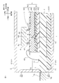
- FIG. 1 is a cross-sectional view of an embodiment of an optical electric transmission composite module of the present invention.
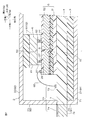
- FIG. 2 is a cross-sectional view of a modified example of the optical and electrical transmission composite module shown in FIG.
- FIG. 3 is a cross-sectional view of a modified example of the optical and electrical transmission composite module shown in FIG.
- FIG. 4 is a cross-sectional view of a further modification of the optical and electrical transmission composite module shown in FIG.
- FIG. 5 is a cross-sectional view of a further modification of the optical and electrical transmission composite module shown in FIG.
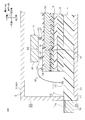
- FIG. 6 is a cross-sectional view of the optical electric transmission composite module of Comparative Example 1.
- the optical electric transmission composite module 1 has a predetermined thickness and has a shape extending in the longitudinal direction.
- the opto-electric transmission composite module 1 converts the transmitted light into electricity and transmits it, and also converts the transmitted electricity into light and transmits the light.
- the optical / electrical transmission composite module 1 includes a housing 2, a heat dissipation layer 3 as an example of a heat dissipation member, a printed wiring board 4, an optical / electrical mixed circuit board 5, and a photoelectric conversion unit 6.
- the housing 2 has a substantially flat box shape whose thickness direction length is shorter than the width direction (direction orthogonal to the thickness direction and the longitudinal direction).
- the housing 2 integrally includes at least a first wall 21, a second wall 22, a connecting wall 23, a second connecting wall (not shown), and both side walls (not shown).
- the first wall 21 has a flat plate shape extending along the longitudinal direction.
- the second wall 22 is arranged to face one side of the first wall 21 in the thickness direction at intervals.
- the shape of the second wall 22 is the same as that of the first wall 21.
- the connecting wall 23 connects the one end edge in the longitudinal direction of the first wall 21 and the one end edge in the longitudinal direction of the second wall 22 in the thickness direction.
- the connecting wall 23 has a flat plate shape extending in the width direction.
- a hole 7 into which one end of the printed wiring board 4 is inserted is formed in the intermediate portion of the connecting wall 23 in the thickness direction. The hole 7 penetrates the connecting wall 23 in the longitudinal direction.
- the second connecting wall (not shown) connects the other end edge of the first wall 21 in the longitudinal direction and the other end edge of the second wall 22 in the longitudinal direction in the thickness direction.
- the second connecting wall extends in the width direction, and its outer shape is the same as that of the connecting wall 23.
- Both side walls connect one end edge in the width direction of the first wall 21 and one end edge in the width direction of the second wall 22 in the thickness direction, and also connect the other end edge in the width direction of the first wall 21 and the first wall.
- the other end edge of the two walls 22 in the width direction is connected in the thickness direction.
- both side walls are continuous with the widthwise both end edges of the connecting wall 23 and the widthwise both end edges of the second connecting wall (not shown). Each of the side walls extends in the longitudinal direction.
- the housing 2 includes a first wall 21, a first member 91 including a connecting wall 23, a second connecting wall, and a part of both side walls (the other side portion in the thickness direction), a second wall 22, and a second wall. It may be composed of two members with a second member 92 including the two connecting walls and the rest of both side walls (one side portion in the thickness direction).
- the housing 2 is made of metal. That is, the material of the housing 2 is metal.
- the metal include aluminum, copper, silver, zinc, nickel, chromium, titanium, tantalum, platinum, gold, and alloys thereof (brass, copper, stainless steel, etc.). Alloys are preferred, and brass (copper and zinc alloys) is more preferred.
- the heat radiating layer 3 has a predetermined thickness and has a shape extending in the longitudinal direction.
- the heat radiating layer 3 is housed in the housing 2. Specifically, the heat radiating layer 3 is in contact with one surface of the first wall 21 in the thickness direction. Specifically, the heat radiating layer 3 is in contact with all of one surface of the first wall 21 in the thickness direction.
- the heat radiating layer 3 includes, for example, a heat radiating sheet, heat radiating grease, a heat radiating plate, and the like. Examples of the material of the heat radiating sheet include a filler resin composition in which the filler is dispersed in the resin.
- the filler examples include alumina (aluminum oxide), boron nitride, zinc oxide, aluminum hydroxide, molten silica, magnesium oxide, aluminum nitride, carbon fiber and the like.
- the resin examples include silicone resin, epoxy resin, acrylic resin, urethane resin and the like, and epoxy resin is preferable.
- a curing agent may be added to the epoxy resin.
- the heat radiating sheet includes, for example, an anisotropic filler such as boron nitride or carbon fiber oriented in the thickness direction in order to obtain high thermal conductivity.
- the filler may be oriented in the thickness direction with respect to the resin.
- the resin contains a thermosetting resin and is in the B stage or the C stage. Further, the resin can include a thermoplastic resin. The ratio of the filler and the resin is appropriately adjusted so as to have the Asker C hardness and the thermal conductivity described later.
- the Ascar C hardness of the heat radiating layer 3 is, for example, 75 or less, preferably 55 or less, more preferably 50 or less, still more preferably 40 or less, and for example, 1 or more.
- the Asker C hardness of the heat radiating layer 3 is determined by the Asker rubber hardness tester C type. When the Ascar C hardness of the heat radiating layer 3 is equal to or less than the above-mentioned upper limit, the heat radiating layer 3 can be brought into close contact with the first wall 21 and the printed wiring board 4, and therefore the heat radiating property of the heat radiating layer 3 can be improved.
- the thermal conductivity of the heat radiating layer 3 in the thickness direction is, for example, 1 W / m ⁇ K or more, preferably 5 W / m ⁇ K or more, more preferably 8 W / m ⁇ K or more, still more preferably 10 W / m ⁇ K. It is K or more, and for example, 200 W / m ⁇ K or less.
- the thermal conductivity of the heat radiating layer 3 is determined by a steady-state method based on ASTM-D5470 or a hot disk method based on ISO-22007-2. If the thermal conductivity of the heat radiating layer 3 is equal to or higher than the above-mentioned lower limit, the heat generated by the photoelectric conversion unit 6 can be efficiently dissipated through the heat radiating layer 3.
- the thickness of the heat radiating layer 3 is, for example, 100 ⁇ m or more, preferably 300 ⁇ m or more, and for example, 3000 ⁇ m or less, preferably 1000 ⁇ m or less.
- a commercially available product can be used for the heat radiating layer 3.
- the printed wiring board 4 has a predetermined thickness and has a shape extending in the longitudinal direction. A portion (a part of an example) other than the protruding end portion 76 described later in the printed wiring board 4 is housed in the housing 2.
- the printed wiring board 4 has an outer shape that is substantially rectangular in a plan view.
- the printed wiring board 4 is in contact with one surface of the heat radiating layer 3 in the thickness direction.
- the printed wiring board 4 includes a support plate 71 and a conductor circuit 72.
- the support plate 71 is parallel to the first wall 21 and has a shape extending in the longitudinal direction.
- the support plate 71 includes a protruding end portion 76.
- the protruding end portion 76 is provided at the one-sided end portion in the longitudinal direction of the support plate 71, and projects from the connecting wall 23 toward one side in the longitudinal direction.
- Examples of the material of the support plate 71 include a hard material such as a glass fiber reinforced epoxy resin.
- the shore A hardness of the support plate 71 is, for example, 80 or more, further 90 or more, and 200 or less, for example.
- Shore A hardness of the support plate 71 is equal to or higher than the above-mentioned lower limit, the strength of the protruding end portion 76 can be ensured, and the photoelectric mixed mounting substrate 5 and the photoelectric conversion portion 6 can be reliably supported.
- Shore A hardness is measured based on JIS K 6253-3 (2012) using a durometer (spring type rubber hardness tester).
- the conductor circuit 72 is arranged on one side of the support plate 71 in the thickness direction.
- the conductor circuit 72 includes a third terminal 73, a fourth terminal 74, and wiring (not shown).
- the third terminal 73 is housed in the housing 2.
- the third terminal 73 is arranged on the other side of the connecting wall 23 in the longitudinal direction at intervals.
- the fourth terminal 74 is arranged on one side of the protruding end portion 76 in the thickness direction.
- Wiring (not shown) connects the third terminal 73 and the fourth terminal 74.
- Examples of the material of the conductor circuit 72 include a conductor such as copper.
- the thickness of the printed wiring board 4 is, for example, 100 ⁇ m or more, preferably 500 ⁇ m or more, more preferably 1,000 ⁇ m or more, and for example, 10,000 ⁇ m or less.
- the optical / electric mixed board 5 is housed in the housing 2 and mounted on the printed wiring board 4.
- the photoelectric mixed mounting substrate 5 has a predetermined thickness and has a flat plate shape extending in the longitudinal direction. Specifically, the optical / electric mixed circuit board 5 is in contact with one surface of the printed wiring board 4 in the thickness direction.
- the optical / electric mixed board 5 includes an optical waveguide 51 and an electric circuit board 52 in order toward one side in the thickness direction.
- the optical waveguide 51 has a predetermined thickness and has a shape extending along the longitudinal direction.
- the optical waveguide 51 is in contact with one side of the printed wiring board 4 in the thickness direction.
- the optical waveguide 51 includes an underclad layer 53, a core layer 54, and an overclad layer 55.
- the underclad layer 53 has the same shape as the optical waveguide 51 in a plan view.
- the core layer 54 is arranged at the center of the underclad layer 53 in the width direction of the other surface in the thickness direction.
- the width of the core layer 54 is narrower than the width of the underclad layer 53 in a plan view.
- the overclad layer 55 is arranged so as to cover the core layer 54 on the other surface of the underclad layer 53 in the thickness direction.
- the overclad layer 55 has the same shape as the outer shape of the underclad layer 53 in a plan view. Specifically, the overclad layer 55 is arranged on the other surface in the thickness direction and both side surfaces in the width direction of the core layer 54, and both outer portions in the width direction of the core layer 54 on the other surface in the thickness direction of the underclad layer 53. There is. Further, the overclad layer 55 is in contact with one surface of the printed wiring board 4 in the thickness direction.
- a mirror 16 is formed at one end in the longitudinal direction of the core layer 54.
- Examples of the material of the optical waveguide 51 include a transparent material such as an epoxy resin.
- the refractive index of the core layer 54 is higher than the refractive index of the underclad layer 53 and the refractive index of the overclad layer 55.
- the thickness of the optical waveguide 51 is, for example, 20 ⁇ m or more, for example, 200 ⁇ m or less.
- the electric circuit board 52 has the same shape as the optical / electric mixed board 5 in a plan view. That is, the electric circuit board 52 has a predetermined thickness and has a flat plate shape extending in the longitudinal direction. It is arranged on one side of the optical waveguide 51 in the thickness direction.
- the electric circuit board 52 includes a metal support layer 56, a base insulating layer 57, a conductor layer 58, and a cover insulating layer (not shown).
- the metal support layer 56 has the same outer shape as the photoelectric mixed substrate 5 in a plan view.
- the optical waveguide 51 is the outermost side portion of the optical / electrical mixed substrate 5 in the thickness direction. Therefore, the metal support layer 56 is in contact with the underclad layer 53.
- Examples of the material of the metal support layer 56 include a metal such as stainless steel.
- the thickness of the metal support layer 56 is, for example, 3 ⁇ m or more, and 100 ⁇ m or less, for example.
- the metal support layer 56 includes a through hole 8 penetrating in the thickness direction. The through hole 8 overlaps with the mirror 16 when projected in the thickness direction.
- the base insulating layer 57 has the same outer shape as the metal support layer 56 in a plan view.
- the base insulating layer 57 is arranged on one side of the metal support layer 56 in the thickness direction. Specifically, the base insulating layer 57 contacts all of one surface of the metal support layer 56 in the thickness direction. Further, the base insulating layer 57 closes one end edge of the through hole 8 in the thickness direction.
- Examples of the material of the base insulating layer 57 include a resin such as polyimide.
- the thickness of the base insulating layer 57 is, for example, 5 ⁇ m or more, and 40 ⁇ m or less, for example.
- the conductor layer 58 is arranged on one side of the base insulating layer 57 in the thickness direction.
- the conductor layer 58 includes a first terminal 27, a second terminal 28, and wiring (not shown).
- the first terminal 27 is arranged corresponding to the photoelectric conversion unit 6 described below.
- a plurality of first terminals 27 are arranged at intervals from each other.
- the second terminal 28 is arranged on one side of the first terminal 27 in the longitudinal direction at intervals.
- the second terminal 28 is electrically connected to the third terminal 73 via a wire 65.
- Wiring (not shown) connects the first terminal 27 and the second terminal 28.
- Examples of the material of the conductor layer 58 include a conductor such as copper.
- the thickness of the conductor layer 58 is, for example, 3 ⁇ m or more, and 20 ⁇ m or less, for example.
- the cover insulation layer (not shown) covers the wiring (not shown). It is arranged on one side of the base insulating layer 57 in the thickness direction.
- the material and thickness of the cover insulating layer are the same as those of the base insulating layer 57.
- the thickness of the photoelectric mixed substrate 5 is, for example, 20 ⁇ m or more, and for example, 200 ⁇ m or less.
- the photoelectric conversion unit 6 is housed in the housing 2 and is mounted on the opto-electric mixed mounting substrate 5.
- the photoelectric conversion unit 6 is arranged to face one side of the first terminal 27 in the thickness direction.
- the photoelectric conversion unit 6 includes a light receiving / receiving member 61 and a bump 62.
- the light emitting / receiving member 61 has a substantially flat rectangular shape extending in the longitudinal direction and the width direction.
- the light receiving / receiving member 61 includes a light receiving / receiving port 63.
- a plurality (for example, four) light receiving / receiving ports 63 are provided on the other surface of the light emitting / receiving member 61 in the thickness direction at intervals from each other.
- the light receiving / receiving port 63 overlaps with the through hole 8 when projected in the thickness direction.
- the optical waveguide 51 of the optical / electrical mixed substrate 5 is optically connected to the photoelectric conversion unit 6.
- the light emitting / receiving member 61 does not overlap with the second terminal 28 when projected in the thickness direction, and is displaced to the other side in the longitudinal direction.
- Examples of the light emitting / receiving member 61 include a light emitting element that converts electricity into light, and specific examples thereof include a surface light emitting diode (VECSEL). Further, examples of the light receiving / receiving member 61 include a light receiving element that converts light into electricity, and specific examples thereof include a photodiode (PD). These can be used alone or in combination.
- a light emitting driving element specifically, Driver IC
- a light receiving driving element specifically, TIA
- the bump 62 is provided so as to project from the other side in the thickness direction of the light emitting / receiving member 61 toward the other side in the thickness direction.
- the bump 62 is located around the light receiving / receiving port 63.
- the length (length in the thickness direction, thickness) of the bump 62 is, for example, 1 ⁇ m or more, and for example, 100 ⁇ m or less.
- Examples of the material of the bump 62 include conductors such as copper, gold, and solder.
- the bump 62 comes into contact with the first terminal 27. As a result, the light emitting / receiving member 61 of the photoelectric conversion unit 6 is electrically connected to the electric circuit board 52 of the optical / electric mixed board 5.
- the light emitting / receiving member 61, the bump 62, and the mounting portion of the photoelectric mixed mounting substrate 5 are fixed and reinforced by an adhesive.
- the first wall 21, the heat dissipation layer 3, the printed wiring board 4, the optical / electrical mixed circuit board 5 and the photoelectric conversion unit 6 are arranged in this order toward one side in the thickness direction.
- the heat radiating layer 3 is arranged on the first wall 21 of the housing 2.
- the heat radiating layer 3 is arranged on one side of the first wall 21 in the thickness direction. Specifically, the heat radiating layer 3 is attached to one surface of the first wall 21 in the thickness direction.
- the housing 2 is composed of two members (first member 91 and second member 92)
- one end surface of the heat radiating layer 3 in the longitudinal direction is the inner surface of the connecting wall 23 and both side walls of the first member 91. To contact.
- the printed wiring board 4 is arranged on one side of the heat radiating layer 3 in the thickness direction. Specifically, when the first wall 21 is included in the first member 91, a portion of the support plate 71 other than the protruding end portion 76 is attached to the heat radiation layer 3, and the protruding end portion 76 is a connecting wall.
- the printed wiring board 4 is installed on the housing 2 (first member 91) and the heat radiating layer 3 so as to protrude from 23.
- the photoelectric mixed mounting substrate 5 and the photoelectric conversion unit 6 are prepared.
- the optical waveguide 51 is provided on the electric circuit board 52 by a known method. Further, the bump 62 is arranged at the first terminal 27, and then the light emitting / receiving member 61 is connected to the bump 62 to mount the photoelectric conversion unit 6 on the optical / electrical mixed mounting substrate 5. As a result, the photoelectric mixed mounting substrate 5 on which the photoelectric conversion unit 6 is mounted is prepared.
- the optical / electrical mixed board 5 on which the photoelectric conversion unit 6 is mounted is mounted on the printed wiring board 4.
- the optical waveguide 51 is fixed to the printed wiring board 4 (bonded via an adhesive (not shown)), and the second terminal 28 and the third terminal 73 are connected via a wire 65.
- the second member 92 including the second wall 22 is arranged on the first member 91. Specifically, the connecting wall 23 of the second member, the second connecting wall (not shown) and both side walls (not shown) are joined to the connecting wall 23 of the first member 91, the second connecting wall (not shown) and both side walls (not shown). .. As a result, the housing 2 is manufactured.
- the opto-electric transmission composite module 1 including the housing 2, the heat-dissipating layer 3, the printed wiring board 4, the opto-electric mixed circuit board 5, and the photoelectric conversion unit 6 is manufactured.
- the material of the heat radiating layer 3 is a filler resin composition containing a resin, and since the heat radiating layer 3 has an appropriate softness, the heat radiating layer 3 is the first wall 21 and the printed wiring board. Can flexibly contact both of 4. Specifically, if the Asker C hardness of the heat radiating layer 3 is as low as 75 or less, the heat radiating layer 3 can be surely adhered to the first wall 21 and the printed wiring board 4, and therefore the heat radiating property can be improved.
- thermo conductivity of the heat radiating layer 3 is 5 W / m ⁇ K or more, the heat generated in the photoelectric conversion unit 6 can be released more efficiently.
- the optical electric transmission composite module 1 shown in FIG. 2 further includes a second heat radiating layer 80 as an example of the second heat radiating member.
- the second heat radiating layer 80 is interposed between the photoelectric conversion unit 6 and the second wall 22 and comes into contact with them. Further, the second heat radiating layer 80 comes into contact with at least one surface of the light emitting / receiving member 61 in the thickness direction. As shown by the virtual line in FIG. 2, the second heat radiating layer 80 may further come into contact with the peripheral side surfaces (both sides in the longitudinal direction and both sides in the width direction) of the light emitting / receiving member 61. In this case, the second heat radiating layer 80 also comes into contact with one side of the electric circuit board 52 around the photoelectric conversion unit 6 in the thickness direction.
- the physical characteristics of the second heat radiating layer 80 are the same as those of the heat radiating layer 3.
- the Asker C hardness of the second heat radiating layer 80 is not more than the above upper limit (preferably 50 or less)
- the second heat radiating layer 80 can flexibly contact the light emitting / receiving member 61 of the photoelectric conversion unit 6.
- the photoelectric conversion unit 6 can suppress damage caused by contact with the second heat radiating layer 80.
- the second heat radiating layer 80 tends to damage the photoelectric conversion unit 6.
- the second heat dissipation layer 80 has the low Asker C hardness (for example, 55 or less) described above, damage to the photoelectric conversion unit 6 can be efficiently suppressed.
- the heat radiating layer 3 is arranged on the first wall 21, the printed wiring board 4 is arranged on the heat radiating layer 3, and the photoelectric conversion unit 6 is mounted.
- the photoelectric mixed board 5 is arranged on the printed wiring board 4, and then the second heat radiating layer 80 is arranged on the photoelectric conversion unit 6.
- the second heat radiating layer 80 is formed in a sheet shape from the same material as the heat radiating layer 3.
- the second member 92 including the second wall 22 is connected to the first member 91.
- the second wall 22 pushes, for example, the second heat radiating layer 80 of the B stage toward the other side in the thickness direction.
- the second heat radiating layer 80 is deformed, it comes into contact with the peripheral side surface of the light emitting / receiving member 61 and one surface of the photoelectric mixed mounting substrate 5 around the light emitting / receiving member 61 in the first direction.
- an optical / electrical transmission composite module 1 including a housing 2, a heat radiating layer 3, a printed wiring board 4, an optical / electric mixed circuit board 5, a photoelectric conversion unit 6, and a second heat radiating layer 80 is obtained.
- the photoelectric transmission composite module 1 further includes a second heat radiating layer 80, and since the second heat radiating layer 80 comes into contact with the second wall 22, the heat generated by the photoelectric conversion unit 6 is released more efficiently. Can be done. That is, the heat of the photoelectric conversion unit 6 can be efficiently dissipated to the housing 2 by the heat radiating layer 3 and the second heat radiating layer 80.
- the second heat radiating layer 80 can flexibly contact the photoelectric conversion unit 6. Therefore, damage to the photoelectric conversion unit 6 can be suppressed.
- the optical / electrical transmission composite module 1 may include a first terminal 27 and a second terminal 28 that are electrically connected to the photoelectric conversion unit 6, and the optical / electrical mixed board 5 still mounts the photoelectric conversion unit 6. It does not have to be.
- the arrangement of the optical waveguide 51, the electric circuit board 52, and the photoelectric conversion unit 6 in the thickness direction may be reversed.
- the optical waveguide 51, the electric circuit board 52, and the photoelectric conversion unit 6 are arranged in order toward the other side in the thickness direction.
- the printed wiring board 4 has a through hole 41 penetrating in the thickness direction.
- the photoelectric conversion unit 6 is arranged in the through hole 41.
- the third terminal 73 is located on one side of the through hole 41 in the longitudinal direction and is arranged in the vicinity of the through hole 41. Further, the electric circuit board 52 is fixed to one surface of the photoelectric conversion portion 6 around the through hole 41 in the thickness direction via an adhesive 42.
- the heat radiating layer 3 has the other surface in the thickness direction and the inner surface of the through hole 41 in the printed wiring board 4, the other surface and the outer peripheral surface in the thickness direction of the photoelectric conversion unit 6, and the periphery of the photoelectric conversion unit 6. Contact with the other surface of the electric circuit board 52 in the thickness direction.
- the second heat radiating layer 80 is arranged between the second wall 22 and the optical waveguide 51.
- the second heat radiating layer 80 comes into contact with the second wall 22 and the optical waveguide 51.
- the first wall 21 has a first protruding portion 25.
- the second wall 22 has a second protrusion 26.
- the first protruding portion 25 projects toward one side in the thickness direction on the first wall 21.
- the first protruding portion 25 comes into contact with the heat radiating layer 3.
- the second protruding portion 26 projects toward the other side in the thickness direction on the second wall 22.
- the second protruding portion 26 comes into contact with the second heat radiating layer 80.
- Preparation Example 2 An appropriate amount of alumina (DAM-70 manufactured by Denka Co., Ltd.) as a filler, an epoxy resin (jER828 manufactured by Mitsubishi Chemical Corporation) and a curing agent (SI-60, SI-S manufactured by Sanshin Chemical Co., Ltd.) were mixed as a resin to prepare a varnish. .. Next, the varnish was formed into a film having a thickness of about 1 mm with an applicator, and then heated in an oven at 80 ° C. for 30 minutes to prepare a heat radiating sheet B.
- DAM-70 manufactured by Denka Co., Ltd. a filler
- an epoxy resin jER828 manufactured by Mitsubishi Chemical Corporation
- SI-60 SI-S manufactured by Sanshin Chemical Co., Ltd.
- Preparation Example 3 A heat radiating sheet C was prepared in the same manner as in Preparation Example 1 except that the amount of alumina blended was reduced so that the thermal conductivity was lower than the thermal conductivity of the heat radiating sheet B of Preparation Example 2.
- Examples 1-3 The optical electric transmission composite module 1 of the embodiment shown in FIG. 1 was manufactured.
- Example 1 the heat radiating sheet A was used for producing the heat radiating layer 3.
- Example 2 the heat radiating sheet B was used for producing the heat radiating layer 3.
- Example 3 the heat radiating sheet C was used for producing the heat radiating layer 3.
- Examples 4-6 An optical electric transmission composite module 1 of a modified example shown in FIG. 2 was manufactured.
- the optical electric transmission composite module 1 further includes a second heat radiating layer 80.
- Example 4 two heat radiating sheets A were used for manufacturing the heat radiating layer 3 and the second heat radiating layer 80.
- Example 5 two heat radiating sheets B were used for manufacturing the heat radiating layer 3 and the second heat radiating layer 80.
- Example 6 two heat radiating sheets C were used for manufacturing the heat radiating layer 3 and the second heat radiating layer 80.
- Comparative Example 1 The optical electric transmission composite module 1 shown in FIG. 6 was manufactured in the same manner as in the first embodiment except that the arrangement of the printed wiring board 4 and the heat radiating layer 3 in the thickness direction was exchanged.
- the first wall 21, the printed wiring board 4, the heat-dissipating layer 3, the opto-electrical mixed circuit board 5, and the photoelectric conversion unit 6 are arranged in this order toward one side in the thickness direction.
- the heat radiating layer 3 is not in contact with the first wall 21.
- the temperature of the light emitting element during driving was calculated by simulation, and the heat dissipation was evaluated.
- a model provided with a photoelectric conversion unit 6 including a light emitting element, a light emitting driving element, a light receiving element, and a light receiving driving element was used, and the environment was cooled at a wind speed of 0.1 m / s.
- ⁇ The temperature of the light emitting element was less than 50 ° C.
- ⁇ The temperature of the light emitting element was 50 ° C. or higher and lower than 55 ° C.
- ⁇ The temperature of the light emitting element was 55 ° C. or higher and lower than 60 ° C.
- X The temperature of the light emitting element was 60 ° C. or higher.
- the optical and electrical transmission composite module is used for signal transmission.
- Optical-electric transmission composite module 2 Housing 3 Heat-dissipating layer 4 Printed wiring board 5 Optical-electric mixed board 6 Photoelectric conversion unit 21 1st wall 22 2nd wall 51 Optical waveguide 52 Electric circuit board 80 2nd heat-dissipating layer
Landscapes
- Physics & Mathematics (AREA)
- General Physics & Mathematics (AREA)
- Optics & Photonics (AREA)
- Engineering & Computer Science (AREA)
- Microelectronics & Electronic Packaging (AREA)
- Thermal Sciences (AREA)
- Optical Couplings Of Light Guides (AREA)
- Cooling Or The Like Of Semiconductors Or Solid State Devices (AREA)
- Optical Integrated Circuits (AREA)
Abstract
Description
本発明の光電気伝送複合モジュールの一実施形態を、図1を参照して説明する。
そして、光電気伝送複合モジュール1では、放熱層3が、第1壁21およびプリント配線板4に接触しているので、光電変換部6で発生し、光電気混載基板5およびプリント配線板4を経由して放熱層3に至った熱を、第1壁21に効率よく逃がすことができる。そのため、光電変換部6が効率よく動作でき、さらには、光電変換部6の熱を筐体2に効率的に逃がすことができる。
以下の各変形例において、上記した一実施形態と同様の部材および工程については、同一の参照符号を付し、その詳細な説明を省略する。また、一実施形態および各変形例を適宜組み合わせることができる。さらに、各変形例は、特記する以外、一実施形態と同様の作用効果を奏することができる。
放熱シートとしてLiPOLY社製PK95を使用した。(放熱シートA)
フィラーとしてアルミナ(デンカ社製DAM-70)と、樹脂としてエポキシ樹脂(三菱ケミカル社製jER828)および硬化剤(三新化学社製SI-60, SI-S)とを適量配合しワニスを調製した。次いで、ワニスを、アプリケーターで1mm程度の厚みに成膜した後、80℃のオーブンで30分加熱し、放熱シートBを作製した。
熱伝導率が、調製例2の放熱シートBの熱伝導率より低くなるように、アルミナの配合量を減らした以外は、調製例1と同様に処理して放熱シートCを作製した。
放熱シートおよび第2放熱シートの物性を表1に記載する。
図1に示す一実施形態の光電気伝送複合モジュール1を製造した。
図2に示す変形例の光電気伝送複合モジュール1を製造した。この光電気伝送複合モジュール1は、第2放熱層80をさらに備える。
プリント配線板4と放熱層3との厚み方向における配置を入れ替えた以外は、実施例1と同様にして、図6に示す光電気伝送複合モジュール1を製造した。
下記の項目を評価した。
光電変換部6を駆動して、下記の基準で放熱性を評価した。
◎:発光素子の温度が50℃未満であった。
○:発光素子の温度が50℃以上55℃未満であった。
△:発光素子の温度が55℃以上60℃未満であった。
×:発光素子の温度が60℃以上であった。
光電変換部6を観察し、下記の基準で損傷を評価した。
◎:光電変換部6の損傷が全く観察されなかった。
○:光電変換部6の損傷がわずかに観察された。

2 筐体
3 放熱層
4 プリント配線板
5 光電気混載基板
6 光電変換部
21 第1壁
22 第2壁
51 光導波路
52 電気回路基板
80 第2放熱層
Claims (5)
- 光電変換部と光学的および電気的に接続されるように構成され、光導波路および電気回路基板を厚み方向一方側に向かって順に含む光電気混載基板と、
前記電気回路基板と電気的に接続されるプリント配線板と、
放熱部材と、
前記光電気混載基板、前記プリント配線板および前記放熱部材の一部を収容する金属製の筐体であって、第1壁を含む前記筐体とを備え、
前記第1壁、前記放熱部材、前記プリント配線板と、前記光電気混載基板とが、前記厚み方向一方側に向かって順に配置され、
前記放熱部材が、前記第1壁およびプリント配線板に接触していることを特徴とする、
光電気伝送複合モジュール。 - 前記放熱部材の23℃におけるアスカーC硬度が、75以下であることを特徴とする、
請求項1に記載の光電気伝送複合モジュール。 - 前記放熱部材の厚み方向の熱伝導率が、5W/m・K以上であることを特徴とする、請求項1または2に記載の光電気伝送複合モジュール。
- 前記光電気混載基板と光学的および電気的に接続される光電変換部と、
前記光電変換部に接触する第2放熱部材をさらに備え、
前記筐体は、前記光電変換部に対して、前記厚み方向において前記第1壁の反対側に配置される第2壁をさらに含み、
前記第2放熱部材が、前記第2壁に接触していることを特徴とする、請求項1~3のいずれか一項に記載の光電気伝送複合モジュール。 - 前記第2放熱部材の23℃におけるアスカーC硬度が、55以下であることを特徴とする、請求項1~4のいずれか一項に記載の光電気伝送複合モジュール。
Priority Applications (4)
| Application Number | Priority Date | Filing Date | Title |
|---|---|---|---|
| US17/911,610 US12289864B2 (en) | 2020-03-19 | 2021-03-17 | Opto-electric transmission composite module |
| KR1020227031855A KR20220156545A (ko) | 2020-03-19 | 2021-03-17 | 광전기 전송 복합 모듈 |
| JP2022508415A JP7681567B2 (ja) | 2020-03-19 | 2021-03-17 | 光電気伝送複合モジュール |
| CN202180021953.4A CN115298589B (zh) | 2020-03-19 | 2021-03-17 | 光电传输复合模块 |
Applications Claiming Priority (2)
| Application Number | Priority Date | Filing Date | Title |
|---|---|---|---|
| JP2020050086 | 2020-03-19 | ||
| JP2020-050086 | 2020-03-19 |
Publications (1)
| Publication Number | Publication Date |
|---|---|
| WO2021187535A1 true WO2021187535A1 (ja) | 2021-09-23 |
Family
ID=77772117
Family Applications (1)
| Application Number | Title | Priority Date | Filing Date |
|---|---|---|---|
| PCT/JP2021/010881 Ceased WO2021187535A1 (ja) | 2020-03-19 | 2021-03-17 | 光電気伝送複合モジュール |
Country Status (6)
| Country | Link |
|---|---|
| US (1) | US12289864B2 (ja) |
| JP (1) | JP7681567B2 (ja) |
| KR (1) | KR20220156545A (ja) |
| CN (1) | CN115298589B (ja) |
| TW (1) | TWI906269B (ja) |
| WO (1) | WO2021187535A1 (ja) |
Families Citing this family (3)
| Publication number | Priority date | Publication date | Assignee | Title |
|---|---|---|---|---|
| JP7359579B2 (ja) * | 2019-07-05 | 2023-10-11 | 日東電工株式会社 | 光電気複合伝送モジュール |
| JP7477310B2 (ja) * | 2020-01-23 | 2024-05-01 | 日東電工株式会社 | 光電変換モジュール |
| JPWO2021162108A1 (ja) * | 2020-02-12 | 2021-08-19 |
Citations (11)
| Publication number | Priority date | Publication date | Assignee | Title |
|---|---|---|---|---|
| JP2006270036A (ja) * | 2005-02-28 | 2006-10-05 | Sony Corp | ハイブリットモジュール及びその製造方法 |
| JP2007142477A (ja) * | 2007-02-27 | 2007-06-07 | Kyocera Corp | 発光装置 |
| JP2009003253A (ja) * | 2007-06-22 | 2009-01-08 | Hitachi Ltd | 光電気混載基板と光電気パッケージとの構造体 |
| US20110044369A1 (en) * | 2009-08-20 | 2011-02-24 | International Business Machines Corporation | Silicon carrier optoelectronic packaging |
| JP2013134347A (ja) * | 2011-12-26 | 2013-07-08 | Fujikura Ltd | 光モジュール |
| JP2013219357A (ja) * | 2012-04-09 | 2013-10-24 | Lg Innotek Co Ltd | 発光素子パッケージ |
| WO2015008555A1 (ja) * | 2013-07-19 | 2015-01-22 | シャープ株式会社 | 発光装置 |
| JP2015022129A (ja) * | 2013-07-18 | 2015-02-02 | 富士通コンポーネント株式会社 | 光モジュール |
| JP2015065293A (ja) * | 2013-09-25 | 2015-04-09 | 株式会社フジクラ | 光学素子実装モジュール、および光学素子実装モジュールの製造方法 |
| JP2016027613A (ja) * | 2014-05-21 | 2016-02-18 | 日本電気硝子株式会社 | 波長変換部材及びそれを用いた発光装置 |
| JP2018093007A (ja) * | 2016-12-01 | 2018-06-14 | 富士通株式会社 | 光モジュール及び光モジュールの製造方法 |
Family Cites Families (17)
| Publication number | Priority date | Publication date | Assignee | Title |
|---|---|---|---|---|
| WO2002093223A1 (en) * | 2001-05-16 | 2002-11-21 | Motorola Broadband Nürnberg GmbH | Device for holding an optical fiber |
| JP3982362B2 (ja) * | 2002-08-23 | 2007-09-26 | 住友電気工業株式会社 | 光データリンク |
| US20070080458A1 (en) | 2005-10-11 | 2007-04-12 | Tsuyoshi Ogawa | Hybrid module and method of manufacturing the same |
| US7936062B2 (en) | 2006-01-23 | 2011-05-03 | Tessera Technologies Ireland Limited | Wafer level chip packaging |
| JP2010211179A (ja) * | 2009-02-13 | 2010-09-24 | Hitachi Ltd | 光電気複合配線モジュールおよびその製造方法 |
| US20130107463A1 (en) * | 2010-07-14 | 2013-05-02 | Sharp Kabushiki Kaisha | Electronic device and display device |
| US8710526B2 (en) | 2011-08-30 | 2014-04-29 | Abl Ip Holding Llc | Thermal conductivity and phase transition heat transfer mechanism including optical element to be cooled by heat transfer of the mechanism |
| WO2013099415A1 (ja) | 2011-12-26 | 2013-07-04 | 株式会社フジクラ | 光モジュール |
| JP6024364B2 (ja) * | 2012-10-09 | 2016-11-16 | 日立金属株式会社 | 通信モジュール及び通信装置 |
| US20180194122A1 (en) * | 2015-02-10 | 2018-07-12 | Zeon Corporation | Heat conductive sheet and method of manufacturing the same |
| FI3121630T3 (fi) * | 2015-07-21 | 2023-06-29 | Tyco Electronics Svenska Holdings Ab | Lämmönhallinnaltaan parannettu optoelektroninen moduuli |
| JP6750019B2 (ja) | 2016-08-08 | 2020-09-02 | 積水化学工業株式会社 | 熱伝導シート及びその製造方法 |
| US11081449B2 (en) * | 2016-11-11 | 2021-08-03 | Mitsubishi Electric Corporation | Semiconductor device and method for manufacturing the same and wireless communication apparatus |
| JP6505874B2 (ja) * | 2016-11-30 | 2019-04-24 | 積水化学工業株式会社 | 熱伝導シート |
| JP6941460B2 (ja) * | 2017-03-31 | 2021-09-29 | 日東電工株式会社 | 光電気混載基板および光電気混載基板アセンブリ |
| JP7176842B2 (ja) * | 2017-12-12 | 2022-11-22 | 日東電工株式会社 | 光電気混載基板 |
| CN109031546A (zh) * | 2018-08-16 | 2018-12-18 | 河北华美光电子有限公司 | 可插拔光模块的解锁装置及其应用的可插拔光模块 |
-
2021
- 2021-03-17 CN CN202180021953.4A patent/CN115298589B/zh active Active
- 2021-03-17 WO PCT/JP2021/010881 patent/WO2021187535A1/ja not_active Ceased
- 2021-03-17 US US17/911,610 patent/US12289864B2/en active Active
- 2021-03-17 KR KR1020227031855A patent/KR20220156545A/ko active Pending
- 2021-03-17 JP JP2022508415A patent/JP7681567B2/ja active Active
- 2021-03-19 TW TW110109909A patent/TWI906269B/zh active
Patent Citations (11)
| Publication number | Priority date | Publication date | Assignee | Title |
|---|---|---|---|---|
| JP2006270036A (ja) * | 2005-02-28 | 2006-10-05 | Sony Corp | ハイブリットモジュール及びその製造方法 |
| JP2007142477A (ja) * | 2007-02-27 | 2007-06-07 | Kyocera Corp | 発光装置 |
| JP2009003253A (ja) * | 2007-06-22 | 2009-01-08 | Hitachi Ltd | 光電気混載基板と光電気パッケージとの構造体 |
| US20110044369A1 (en) * | 2009-08-20 | 2011-02-24 | International Business Machines Corporation | Silicon carrier optoelectronic packaging |
| JP2013134347A (ja) * | 2011-12-26 | 2013-07-08 | Fujikura Ltd | 光モジュール |
| JP2013219357A (ja) * | 2012-04-09 | 2013-10-24 | Lg Innotek Co Ltd | 発光素子パッケージ |
| JP2015022129A (ja) * | 2013-07-18 | 2015-02-02 | 富士通コンポーネント株式会社 | 光モジュール |
| WO2015008555A1 (ja) * | 2013-07-19 | 2015-01-22 | シャープ株式会社 | 発光装置 |
| JP2015065293A (ja) * | 2013-09-25 | 2015-04-09 | 株式会社フジクラ | 光学素子実装モジュール、および光学素子実装モジュールの製造方法 |
| JP2016027613A (ja) * | 2014-05-21 | 2016-02-18 | 日本電気硝子株式会社 | 波長変換部材及びそれを用いた発光装置 |
| JP2018093007A (ja) * | 2016-12-01 | 2018-06-14 | 富士通株式会社 | 光モジュール及び光モジュールの製造方法 |
Also Published As
| Publication number | Publication date |
|---|---|
| CN115298589B (zh) | 2026-03-20 |
| CN115298589A (zh) | 2022-11-04 |
| TW202143828A (zh) | 2021-11-16 |
| US12289864B2 (en) | 2025-04-29 |
| JP7681567B2 (ja) | 2025-05-22 |
| JPWO2021187535A1 (ja) | 2021-09-23 |
| US20230118655A1 (en) | 2023-04-20 |
| TWI906269B (zh) | 2025-12-01 |
| KR20220156545A (ko) | 2022-11-25 |
Similar Documents
| Publication | Publication Date | Title |
|---|---|---|
| US10517166B2 (en) | Optical transceiver including heat dissipation structure | |
| WO2021187535A1 (ja) | 光電気伝送複合モジュール | |
| TWI896588B (zh) | 光電轉換模組 | |
| JP2009016682A (ja) | 光モジュールおよび通信装置 | |
| CN110426792A (zh) | 光收发器及其外壳 | |
| JP2020177172A (ja) | 光トランシーバ | |
| JP2019191281A (ja) | 光モジュール、及び光伝送装置 | |
| WO2021145376A1 (ja) | 光電気伝送複合モジュールおよび光電気混載基板 | |
| KR20240146554A (ko) | 광 전기 복합 전송 모듈 및 그것을 사용한 광 통신 케이블 | |
| JP7359579B2 (ja) | 光電気複合伝送モジュール | |
| JP7192343B2 (ja) | 光トランシーバ | |
| JP7372754B2 (ja) | 光電気混載基板 | |
| US20230012678A1 (en) | Opto-electric hybrid board and opto-electric composite transmission module | |
| US20210239926A1 (en) | Optical transceiver | |
| CN118738946A (zh) | 光电复合传输模块以及使用光电复合传输模块的光通信缆线 | |
| JP2021052024A (ja) | 光電気複合伝送モジュール | |
| JP2005269474A (ja) | 光トランシーバ | |
| JP2010113207A (ja) | 光電気変換モジュール | |
| JP2025172585A (ja) | 光電混載基板、光モジュール、および、電子機器 |
Legal Events
| Date | Code | Title | Description |
|---|---|---|---|
| 121 | Ep: the epo has been informed by wipo that ep was designated in this application |
Ref document number: 21770798 Country of ref document: EP Kind code of ref document: A1 |
|
| ENP | Entry into the national phase |
Ref document number: 2022508415 Country of ref document: JP Kind code of ref document: A |
|
| NENP | Non-entry into the national phase |
Ref country code: DE |
|
| 122 | Ep: pct application non-entry in european phase |
Ref document number: 21770798 Country of ref document: EP Kind code of ref document: A1 |
|
| WWG | Wipo information: grant in national office |
Ref document number: 17911610 Country of ref document: US |