WO2021187200A1 - 弾性波装置及び複合フィルタ装置 - Google Patents
弾性波装置及び複合フィルタ装置 Download PDFInfo
- Publication number
- WO2021187200A1 WO2021187200A1 PCT/JP2021/009028 JP2021009028W WO2021187200A1 WO 2021187200 A1 WO2021187200 A1 WO 2021187200A1 JP 2021009028 W JP2021009028 W JP 2021009028W WO 2021187200 A1 WO2021187200 A1 WO 2021187200A1
- Authority
- WO
- WIPO (PCT)
- Prior art keywords
- resonator
- elastic wave
- wave device
- electrode layer
- filter
- Prior art date
- Legal status (The legal status is an assumption and is not a legal conclusion. Google has not performed a legal analysis and makes no representation as to the accuracy of the status listed.)
- Ceased
Links
Images




Classifications
-
- H—ELECTRICITY
- H03—ELECTRONIC CIRCUITRY
- H03H—IMPEDANCE NETWORKS, e.g. RESONANT CIRCUITS; RESONATORS
- H03H9/00—Networks comprising electromechanical or electro-acoustic elements; Electromechanical resonators
- H03H9/02—Details
- H03H9/125—Driving means, e.g. electrodes, coils
- H03H9/145—Driving means, e.g. electrodes, coils for networks using surface acoustic waves
- H03H9/14538—Formation
- H03H9/14541—Multilayer finger or busbar electrode
-
- H—ELECTRICITY
- H03—ELECTRONIC CIRCUITRY
- H03H—IMPEDANCE NETWORKS, e.g. RESONANT CIRCUITS; RESONATORS
- H03H9/00—Networks comprising electromechanical or electro-acoustic elements; Electromechanical resonators
- H03H9/46—Filters
- H03H9/54—Filters comprising resonators of piezoelectric or electrostrictive material
- H03H9/56—Monolithic crystal filters
- H03H9/566—Electric coupling means therefor
- H03H9/568—Electric coupling means therefor consisting of a ladder configuration
-
- H—ELECTRICITY
- H03—ELECTRONIC CIRCUITRY
- H03H—IMPEDANCE NETWORKS, e.g. RESONANT CIRCUITS; RESONATORS
- H03H9/00—Networks comprising electromechanical or electro-acoustic elements; Electromechanical resonators
- H03H9/02—Details
- H03H9/02007—Details of bulk acoustic wave devices
-
- H—ELECTRICITY
- H03—ELECTRONIC CIRCUITRY
- H03H—IMPEDANCE NETWORKS, e.g. RESONANT CIRCUITS; RESONATORS
- H03H9/00—Networks comprising electromechanical or electro-acoustic elements; Electromechanical resonators
- H03H9/02—Details
- H03H9/02535—Details of surface acoustic wave devices
- H03H9/02543—Characteristics of substrate, e.g. cutting angles
- H03H9/02574—Characteristics of substrate, e.g. cutting angles of combined substrates, multilayered substrates, piezoelectrical layers on not-piezoelectrical substrate
-
- H—ELECTRICITY
- H03—ELECTRONIC CIRCUITRY
- H03H—IMPEDANCE NETWORKS, e.g. RESONANT CIRCUITS; RESONATORS
- H03H9/00—Networks comprising electromechanical or electro-acoustic elements; Electromechanical resonators
- H03H9/02—Details
- H03H9/02535—Details of surface acoustic wave devices
- H03H9/02818—Means for compensation or elimination of undesirable effects
-
- H—ELECTRICITY
- H03—ELECTRONIC CIRCUITRY
- H03H—IMPEDANCE NETWORKS, e.g. RESONANT CIRCUITS; RESONATORS
- H03H9/00—Networks comprising electromechanical or electro-acoustic elements; Electromechanical resonators
- H03H9/02—Details
- H03H9/125—Driving means, e.g. electrodes, coils
- H03H9/13—Driving means, e.g. electrodes, coils for networks consisting of piezoelectric or electrostrictive materials
-
- H—ELECTRICITY
- H03—ELECTRONIC CIRCUITRY
- H03H—IMPEDANCE NETWORKS, e.g. RESONANT CIRCUITS; RESONATORS
- H03H9/00—Networks comprising electromechanical or electro-acoustic elements; Electromechanical resonators
- H03H9/15—Constructional features of resonators consisting of piezoelectric or electrostrictive material
- H03H9/205—Constructional features of resonators consisting of piezoelectric or electrostrictive material having multiple resonators
-
- H—ELECTRICITY
- H03—ELECTRONIC CIRCUITRY
- H03H—IMPEDANCE NETWORKS, e.g. RESONANT CIRCUITS; RESONATORS
- H03H9/00—Networks comprising electromechanical or electro-acoustic elements; Electromechanical resonators
- H03H9/70—Multiple-port networks for connecting several sources or loads, working on different frequencies or frequency bands, to a common load or source
- H03H9/703—Networks using bulk acoustic wave devices
Definitions
- the present invention relates to an elastic wave device and a composite filter device in which a first resonator and a second resonator connected in parallel or in series with each other on a piezoelectric layer are configured.
- an electrode is provided on the piezoelectric substrate.
- the electrode has a base electrode layer and a main electrode layer provided on the base electrode layer.
- the main electrode layer is a polycrystalline thin film composed of an epitaxially grown alignment film and having a twin structure in which the diffraction pattern observed in the X-ray diffraction pole diagram has a plurality of symmetrical centers.
- the electrode is a polycrystalline thin film having a twin structure having a plurality of centers of symmetry, stress migration resistance can be improved and power resistance can be improved. It is said that it can be done.
- An object of the present invention is to provide an elastic wave apparatus and a composite filter apparatus capable of improving linearity and reducing harmonic levels in an elastic wave apparatus having a plurality of elastic wave resonators. It is in.
- the elastic wave device according to the present invention is laminated on the piezoelectric layer and the piezoelectric layer, and is laminated on the IDT electrode constituting the first resonator and the piezoelectric layer.
- the IDT electrode constituting the second resonator is provided, and the first resonator and the second resonator are connected in parallel or in series, and the IDT of the first resonator is provided.
- the electrode has an electrode layer made of an epitaxial film, and the IDT electrode of the second resonator has an electrode layer made of a non-piezoelectric film.
- the composite filter device includes the elastic wave filter comprising the elastic wave device configured according to the present invention, and at least one band-passing type filter, and includes the elastic wave filter and at least one other band.
- a pass-through filter is commonly connected at one end.
- the level of harmonics can be reduced by improving the linearity.
- FIG. 1 (a) and 1 (b) are a front sectional view of an elastic wave resonator used in the elastic wave apparatus according to the first embodiment of the present invention and a partially enlarged sectional view of an electrode portion.
- FIG. 2 is a schematic plan view showing an electrode structure in an elastic wave device used in the first embodiment of the present invention.
- FIG. 3 is a schematic circuit diagram of an elastic wave device according to a first embodiment of the present invention.
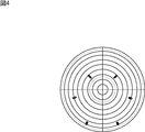
- FIG. 4 is an XRD pole view of the main electrode layer according to the first embodiment of the present invention.
- FIG. 5 is an XRD pole figure when the main electrode layer made of Al is a non-epitaxial film.
- FIG. 6 is a diagram showing the relationship between the frequencies of the first resonator and the second resonator and the third harmonic level.
- FIG. 7 is a diagram showing the relationship between the frequency in the elastic wave device of the first embodiment, Comparative Example 1 and Comparative Example 2, and the level of the third harmonic.
- FIG. 8 is a schematic circuit diagram of the elastic wave device according to the second embodiment.
- FIG. 9 is a circuit diagram of a ladder type filter as a third embodiment of the present invention.
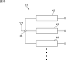
- FIG. 10 is a circuit diagram for explaining a multiplexer as a fourth embodiment of the present invention.
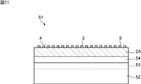
- FIG. 11 is a front sectional view showing a modified example of the elastic wave resonator used in the present invention.
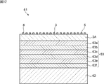
- FIG. 12 is a front sectional view showing another modified example of the elastic wave resonator used in the present invention.
- FIG. 1A is a front sectional view for explaining an elastic wave resonator used in the elastic wave apparatus of the first embodiment of the present invention
- FIG. 1B is a partially enlarged sectional view of the electrode
- FIG. 2 is a schematic plan view showing an electrode structure.
- the elastic wave resonator 1 has a piezoelectric substrate 2 as a piezoelectric layer.
- the piezoelectric substrate 2 is made of LiTaO 3 .
- the piezoelectric substrate 2 may be made of another piezoelectric single crystal such as LiNbO 3.
- An IDT electrode 3 and reflectors 4 and 5 are provided as electrodes on the piezoelectric substrate 2. As a result, a 1-port elastic wave resonator is formed.
- the IDT electrode 3 has first and second electrode fingers 3a and 3b that are interleaved with each other.
- FIG. 1B is a partially enlarged cross-sectional view of a portion where the first electrode finger 3a is provided.
- the base electrode layer 6 and the main electrode layer 7 are laminated on the piezoelectric substrate 2.
- the base electrode layer 6 is made of Ti
- the main electrode layer 7 is made of Al.
- the main electrode layer is an electrode layer that plays a role in exciting elastic waves in the IDT electrode.
- the main electrode layer occupies a ratio of 50% by weight or more in the laminated structure.
- the base electrode layer 6 can be made of various metal materials having better adhesion to the piezoelectric substrate 2 than the main electrode layer other than Ti. For example, NiCr or the like may be used.
- the main electrode layer 7 is made of Al in this embodiment, but may be made of another metal such as Cu, Au, Ag, Pt, Mo, or W. Further, the main electrode layer 7 may be an alloy mainly composed of Al or the above metal.
- At least one other metal layer may be provided between the main electrode layer and the base electrode layer, and on the main electrode layer.
- FIG. 3 is a schematic circuit diagram of an elastic wave device according to the first embodiment of the present invention.
- the first resonator 12 and the second resonator 13 are connected in parallel.
- the first resonator 12 and the second resonator 13 are composed of the above-mentioned 1-port elastic wave resonator.
- the feature of the elastic wave device 11 is that the main electrode layer of the IDT electrode in the first resonator 12 is made of an epitaxial film, and the IDT electrode of the second resonator 13 has a main electrode layer made of a non-epitaxial film. be.
- the linearity is improved, and the level of harmonics when the band-passing type filter is configured can be suppressed.
- the normal line of the crystal plane (for example, the (111) plane in the case of Al) of the main electrode layer 7 substantially coincides with the c-axis of the piezoelectric substrate 2, and the X-ray diffraction pole point diagram (XRD pole point diagram). ) Is a single crystal film having 6-fold symmetrical spots.
- FIG. 4 shows an XRD pole figure of the main electrode layer made of Al in the first embodiment. As is clear from FIG. 4, 6-fold symmetric spots appear.
- the first resonator has a main electrode layer made of such an epitaxial film as described above.
- FIG. 5 is an XRD pole figure when the main electrode layer made of Al is a non-epitaxial film.
- the non-epitaxial film shows a diffraction pattern in which 6-fold symmetric spots do not appear.
- the IDT electrode of the second resonator has a main electrode layer which is a non-epitaxial film.
- FIG. 6 is a diagram showing the relationship between the frequencies of the first resonator and the second resonator and the third harmonic level.
- the solid line shows the relationship for the first resonator
- the broken line shows the relationship for the second resonator.
- the elastic wave resonator 1 is formed by laminating a base electrode layer 6 made of a Ti film having a thickness of 30 nm and a main electrode layer 7 made of an Al film having a thickness of 415 nm on a piezoelectric substrate 2 made of a 42-degree cut LiTaO 3.
- the structure was used.
- the Al film is an epitaxial film
- the Al film is a non-epitaxial film.
- the film formation of the epitaxial film can be carried out by, for example, the method described in JP-A-2002-305402. That is, after the piezoelectric substrate is pretreated by ion etching, a base electrode layer made of Ti is formed. Next, a main electrode layer made of Al is formed. In this case, Al is epitaxially grown so that the (111) plane of the Al crystal is perpendicular to the c-axis of LiTaO 3 on the piezoelectric substrate.
- the non-epitaxial film of the second resonator can be obtained by forming a Ti film as a base electrode layer and an Al film as a main electrode layer without performing the above-mentioned ion etching treatment.
- the method of forming the main electrode layer made of an epitaxial film and the main electrode layer made of a non-epitaxial film is not particularly limited.
- the frequency dependence of the third harmonic level (H3 level) is significantly different between the first resonator having an epitaxial film and the second resonator having a non-epitaxial film. You can see that.
- FIG. 7 shows the frequency of each elastic wave device of Example 1 and the following Comparative Examples 1 and 2 for the elastic wave device according to the first embodiment, and the level of the third harmonic (H3 level). It is a figure which shows the relationship.
- the solid line shows the result of Example 1
- the broken line shows the result of Comparative Example 1
- the alternate long and short dash line shows the result of Comparative Example 2.
- the first resonator 12 and the second resonator 13 are connected in parallel.
- Comparative example 1 Two first resonators are connected in parallel.
- Comparative example 2 Two second resonators are connected in parallel.
- FIG. 8 is a schematic circuit diagram of an elastic wave device according to a second embodiment of the present invention.
- the first resonator 12 and the second resonator 13 are connected in series.
- the first resonator 12 and the second resonator 13 may be connected in parallel or may be connected in series.
- At least one third resonator X may be further connected in parallel, and in the elastic wave device 21, at least one elastic wave resonator is further connected in series. It may have been done.
- FIG. 9 is a circuit diagram of a ladder type filter 31 as a third embodiment of the present invention.
- the ladder type filter 31 is a transmission filter.
- a plurality of elastic wave resonators are connected between the input terminal 32 and the antenna terminal 33. That is, the series arm resonators S1, S2, S3a, and S3b are provided on the series arm connecting the input terminal 32 and the antenna terminal 33. Further, parallel arm resonators P1, P2, and P3 are arranged in a plurality of parallel arms connecting the series arm and the ground potential, respectively. These series arm resonators S1, S2, S3a, S3b and parallel arm resonators P1, P2, P3 are all made of elastic wave resonators.
- the series arm resonator S3a and the series arm resonator S3b are split type elastic wave resonators in which one elastic wave resonator is divided in parallel.
- the series arm resonator S3a and the series arm resonator S3b are parallel division type resonators in which one series arm resonator is divided in parallel, and a path connecting the input terminal 32 and the antenna terminal 33.
- the split type elastic wave resonator is a type of elastic wave resonator connected in parallel or in series so as to have substantially the same impedance as the impedance of the elastic wave resonator before division.
- the total capacitance of the split type elastic wave resonator is substantially equal to the capacitance of the elastic wave resonator before splitting.
- the series arm resonator S3a and the series arm resonator S3b are series division type resonators in which one series arm resonator is divided in series
- the series arm resonator S3a and the series arm resonator S3b are different from each other. They are connected in series with each other on the path connecting the input terminal 32 and the antenna terminal 33, and none of the parallel arm resonators are connected between them.
- any of the parallel arm resonators P1 to P3 may be a split type elastic wave resonator.
- the split type elastic wave resonators are parallel to each other or are connected to each other. They are connected in series.
- the series arm resonator S3a is composed of the first resonator in the present invention
- the series arm resonator S3b is composed of the second resonator in the present invention.
- the series arm resonators S3a and S3b are divided type elastic wave resonators in which one series arm resonator is divided into two, and are configured according to the present invention, so that the linearity can be improved. can. Therefore, in the ladder type filter 31, the level of harmonics can be effectively suppressed, and good filter characteristics can be obtained.
- the resonator closest to the antenna terminal 33 has a great influence on the filter characteristics. Therefore, it is preferable that the series arm resonator S3a and the series arm resonator S3b constituting the elastic wave device configured according to the present invention are elastic wave resonators closest to the antenna terminal 33.
- the elastic wave device of the present invention can be widely applied to a filter having a plurality of elastic wave resonators other than the ladder type filter.
- the split type series arm resonators S3a and S3b connected in parallel are shown.
- the series arm resonator S2 may be split in series with the first and second resonators. ..
- the series arm resonator S2 may be composed of the first resonator
- the parallel arm resonator P3 may be composed of the second resonator. That is, one of the series arm resonator and the parallel arm resonator connected to each other may be the first resonator and the other may be the second resonator. Even in that case, according to the present invention, the level of harmonics can be effectively reduced by improving the linearity.
- FIG. 10 is a circuit diagram for explaining a multiplexer as a fourth embodiment of the present invention.
- band-passing filters 42, 43, 44, ... Of the first, second, third, ... are connected to the antenna terminal 33. That is, one ends of the plurality of band-passing filters 42, 43, 44, ... Are commonly connected.
- the pass bands of the band pass type filters 42, 43, 44, ... Are different from each other.
- an elastic wave filter having an elastic wave device configured according to the present invention may be used as at least one of the bandpass type filters 42, 43, 44 .... Thereby, the filter characteristics in the multiplexer 41 can be improved.
- FIG. 11 is a front sectional view showing a modified example of the elastic wave resonator used in the present invention.
- the bass velocity film 54 and the piezoelectric layer 2A are laminated on the support substrate 52. That is, a thin piezoelectric layer 2A is used instead of the piezoelectric substrate 2 shown in FIG. 1 (a).
- the bass velocity film 54 is arranged between the piezoelectric layer 2A and the support substrate 52.
- the bass velocity film 54 is made of a bass velocity material.
- the support substrate 52 is made of a hypersonic material.
- the low sound velocity material refers to a material in which the sound velocity of the propagating bulk wave is lower than the sound velocity of the bulk wave propagating in the piezoelectric layer 2A.
- the hypersonic material is a material in which the sound velocity of the propagating bulk wave is faster than the sound velocity of the elastic wave propagating in the piezoelectric layer 2A.
- an appropriate material having a bulk wave sound velocity lower than that of the bulk wave propagating in the piezoelectric layer can be used.
- Examples of such a low sound velocity material include silicon oxide, glass, silicon nitride, tantalum oxide, a compound obtained by adding fluorine, carbon, boron, hydrogen, or a silanol group to silicon oxide, and a medium containing the above material as a main component.
- Various materials such as, etc. can be used.
- high-frequency materials examples include aluminum oxide, silicon carbide, silicon nitride, silicon nitride, silicon, sapphire, lithium tantalate, lithium niobate, crystal, alumina, zirconia, cordylite, mulite, steatite, forsterite, and magnesia.
- DLC diamond-like carbon film or diamond, a medium containing the above material as a main component, a medium containing a mixture of the above materials as a main component, and the like can be used.
- the piezoelectric substrate in which the low sound velocity film 54 and the piezoelectric layer 2A are laminated on the support substrate 52 made of the high sound velocity material may be used.
- the hypersonic film 53 shown by the broken line may be laminated between the support substrate 52 and the low sound velocity film 54.
- the hypersonic film 53 is made of the above hypersonic material.
- the support substrate 52 may be made of a material other than the hypersonic material.
- FIG. 12 is a front sectional view showing another modified example of the structure of the elastic wave resonator.
- the acoustic multilayer film 63 is laminated between the piezoelectric layer 2A and the support substrate 62.
- the support substrate 62 is made of an appropriate insulator such as Si or a semiconductor.
- the acoustic multilayer film 63 has low acoustic impedance layers 63a, 63c, 63e having a relatively low acoustic impedance and high acoustic impedance layers 63b, 63d, 63f having a relatively high acoustic impedance.
- the low acoustic impedance layers 63a, 63c, 63e are made of a material having a relatively low acoustic impedance, such as silicon oxide.
- Silicon oxide is represented by SiO x (x is an integer).
- the value of x is not particularly limited, but in the present embodiment, each low acoustic impedance layer is made of SiO 2 .
- the material of the plurality of low acoustic impedance layers is not limited to the above, and may be any material having a relatively low acoustic impedance.
- the high acoustic impedance layers 63b, 63d, 63f may be, for example, a metal such as Pt or W, or a dielectric such as AlN or SiN.
- the material of the plurality of high acoustic impedance layers may be any material having a relatively high acoustic impedance.
- acoustic multilayer film 63 By using the acoustic multilayer film 63, it is possible to confine the excited elastic wave in the piezoelectric layer 2A.
- a piezoelectric substrate having such an acoustic multilayer film 63 may be used.
- a cavity may be used to confine the elastic wave. In this case, a cavity may be formed in the support substrate 62, and the piezoelectric layer 2A may be formed on the support substrate so as to cover the cavity.
- Low-acoustic impedance layers 63b, 63d, 63f High-acoustic impedance layers P1 to P3 ... Parallel arm resonators S1, S2, S3a, S3b ... Series arm resonator
Landscapes
- Physics & Mathematics (AREA)
- Acoustics & Sound (AREA)
- Chemical & Material Sciences (AREA)
- Crystallography & Structural Chemistry (AREA)
- Piezo-Electric Or Mechanical Vibrators, Or Delay Or Filter Circuits (AREA)
- Surface Acoustic Wave Elements And Circuit Networks Thereof (AREA)
Priority Applications (3)
| Application Number | Priority Date | Filing Date | Title |
|---|---|---|---|
| CN202180017643.5A CN115191084A (zh) | 2020-03-18 | 2021-03-08 | 弹性波装置及复合滤波器装置 |
| JP2022508227A JP7428237B2 (ja) | 2020-03-18 | 2021-03-08 | 弾性波装置及び複合フィルタ装置 |
| US17/903,296 US12438521B2 (en) | 2020-03-18 | 2022-09-06 | Acoustic wave device and composite filter device |
Applications Claiming Priority (2)
| Application Number | Priority Date | Filing Date | Title |
|---|---|---|---|
| JP2020047272 | 2020-03-18 | ||
| JP2020-047272 | 2020-03-18 |
Related Child Applications (1)
| Application Number | Title | Priority Date | Filing Date |
|---|---|---|---|
| US17/903,296 Continuation US12438521B2 (en) | 2020-03-18 | 2022-09-06 | Acoustic wave device and composite filter device |
Publications (1)
| Publication Number | Publication Date |
|---|---|
| WO2021187200A1 true WO2021187200A1 (ja) | 2021-09-23 |
Family
ID=77771257
Family Applications (1)
| Application Number | Title | Priority Date | Filing Date |
|---|---|---|---|
| PCT/JP2021/009028 Ceased WO2021187200A1 (ja) | 2020-03-18 | 2021-03-08 | 弾性波装置及び複合フィルタ装置 |
Country Status (4)
| Country | Link |
|---|---|
| US (1) | US12438521B2 (https=) |
| JP (1) | JP7428237B2 (https=) |
| CN (1) | CN115191084A (https=) |
| WO (1) | WO2021187200A1 (https=) |
Families Citing this family (1)
| Publication number | Priority date | Publication date | Assignee | Title |
|---|---|---|---|---|
| CN117559953B (zh) * | 2023-02-15 | 2025-07-08 | 北京芯溪半导体科技有限公司 | 滤波器设计方法、装置及相关设备 |
Citations (7)
| Publication number | Priority date | Publication date | Assignee | Title |
|---|---|---|---|---|
| JP2000349591A (ja) * | 1999-06-08 | 2000-12-15 | Oki Electric Ind Co Ltd | 弾性表面波フィルタを用いた分波器 |
| WO2009063559A1 (ja) * | 2007-11-15 | 2009-05-22 | Fujitsu Limited | 弾性波デバイス、それを用いたデュープレクサおよびそのデュープレクサを用いた通信機 |
| WO2009150786A1 (ja) * | 2008-06-09 | 2009-12-17 | 株式会社村田製作所 | 弾性表面波装置及びその製造方法 |
| JP2011097237A (ja) * | 2009-10-28 | 2011-05-12 | Kyocera Corp | 弾性表面波装置 |
| JP2011211460A (ja) * | 2010-03-30 | 2011-10-20 | Sae Magnetics (Hk) Ltd | 弾性表面波装置 |
| JP2018157510A (ja) * | 2017-03-21 | 2018-10-04 | 太陽誘電株式会社 | マルチプレクサ |
| WO2019111902A1 (ja) * | 2017-12-06 | 2019-06-13 | 株式会社村田製作所 | マルチプレクサ、高周波フロントエンド回路および通信装置 |
Family Cites Families (8)
| Publication number | Priority date | Publication date | Assignee | Title |
|---|---|---|---|---|
| JP2003258594A (ja) | 2001-12-27 | 2003-09-12 | Murata Mfg Co Ltd | 弾性表面波素子およびその製造方法 |
| CN104205633B (zh) * | 2012-03-23 | 2016-10-26 | 株式会社村田制作所 | 弹性波滤波器元件以及其制造方法 |
| WO2016100692A2 (en) * | 2014-12-17 | 2016-06-23 | Rf Micro Devices, Inc. | Plate wave devices with wave confinement structures and fabrication methods |
| US11218133B2 (en) * | 2016-09-30 | 2022-01-04 | Intel Corporation | Film bulk acoustic resonator (FBAR) devices for high frequency RF filters |
| US10483942B2 (en) * | 2017-01-24 | 2019-11-19 | Skyworks Solutions, Inc. | Acoustic wave device with acoustically separated multi-channel feedback |
| DE102018102891A1 (de) * | 2017-02-13 | 2018-08-16 | Murata Manufacturing Co., Ltd. | Multiplexierer, Übertragungsvorrichtung und Empfangsvorrichtung |
| JP2018133800A (ja) * | 2017-02-13 | 2018-08-23 | 株式会社村田製作所 | マルチプレクサ、送信装置および受信装置 |
| JP2018207290A (ja) * | 2017-06-02 | 2018-12-27 | 株式会社村田製作所 | 弾性波共振子および弾性波フィルタ |
-
2021
- 2021-03-08 CN CN202180017643.5A patent/CN115191084A/zh active Pending
- 2021-03-08 WO PCT/JP2021/009028 patent/WO2021187200A1/ja not_active Ceased
- 2021-03-08 JP JP2022508227A patent/JP7428237B2/ja active Active
-
2022
- 2022-09-06 US US17/903,296 patent/US12438521B2/en active Active
Patent Citations (7)
| Publication number | Priority date | Publication date | Assignee | Title |
|---|---|---|---|---|
| JP2000349591A (ja) * | 1999-06-08 | 2000-12-15 | Oki Electric Ind Co Ltd | 弾性表面波フィルタを用いた分波器 |
| WO2009063559A1 (ja) * | 2007-11-15 | 2009-05-22 | Fujitsu Limited | 弾性波デバイス、それを用いたデュープレクサおよびそのデュープレクサを用いた通信機 |
| WO2009150786A1 (ja) * | 2008-06-09 | 2009-12-17 | 株式会社村田製作所 | 弾性表面波装置及びその製造方法 |
| JP2011097237A (ja) * | 2009-10-28 | 2011-05-12 | Kyocera Corp | 弾性表面波装置 |
| JP2011211460A (ja) * | 2010-03-30 | 2011-10-20 | Sae Magnetics (Hk) Ltd | 弾性表面波装置 |
| JP2018157510A (ja) * | 2017-03-21 | 2018-10-04 | 太陽誘電株式会社 | マルチプレクサ |
| WO2019111902A1 (ja) * | 2017-12-06 | 2019-06-13 | 株式会社村田製作所 | マルチプレクサ、高周波フロントエンド回路および通信装置 |
Also Published As
| Publication number | Publication date |
|---|---|
| US12438521B2 (en) | 2025-10-07 |
| CN115191084A (zh) | 2022-10-14 |
| JP7428237B2 (ja) | 2024-02-06 |
| US20220416764A1 (en) | 2022-12-29 |
| JPWO2021187200A1 (https=) | 2021-09-23 |
Similar Documents
| Publication | Publication Date | Title |
|---|---|---|
| CN101796727B (zh) | 弹性边界波装置 | |
| KR102316353B1 (ko) | 탄성파 장치, 필터, 고주파 프론트 엔드 회로 및 통신 장치 | |
| JP4419961B2 (ja) | 弾性境界波装置 | |
| WO2019138810A1 (ja) | 弾性波装置、マルチプレクサ、高周波フロントエンド回路及び通信装置 | |
| WO2020204036A1 (ja) | 弾性波装置 | |
| US12244296B2 (en) | Acoustic wave filter | |
| WO2018164209A1 (ja) | 弾性波装置、弾性波装置パッケージ、高周波フロントエンド回路及び通信装置 | |
| US12289096B2 (en) | Acoustic wave filter device | |
| US20200389147A1 (en) | Acoustic wave device | |
| WO2020261763A1 (ja) | 弾性波装置 | |
| CN113454912B (zh) | 弹性波装置 | |
| JPWO2020209190A1 (ja) | 弾性波装置及びマルチプレクサ | |
| WO2020250572A1 (ja) | 弾性波装置 | |
| WO2022138443A1 (ja) | 弾性波装置 | |
| WO2021039639A1 (ja) | 弾性波装置 | |
| WO2019082806A1 (ja) | 弾性波素子 | |
| JP2024162642A (ja) | 弾性波装置 | |
| JP7428237B2 (ja) | 弾性波装置及び複合フィルタ装置 | |
| US20240162883A1 (en) | Acoustic wave device | |
| JPWO2010125934A1 (ja) | 弾性波装置 | |
| WO2023132354A1 (ja) | フィルタデバイス、分波器および通信装置 | |
| WO2023085189A1 (ja) | フィルタ装置 | |
| WO2022138140A1 (ja) | 複合フィルタ装置 | |
| WO2020241776A1 (ja) | 弾性波装置 | |
| WO2020261808A1 (ja) | 弾性波フィルタ |
Legal Events
| Date | Code | Title | Description |
|---|---|---|---|
| 121 | Ep: the epo has been informed by wipo that ep was designated in this application |
Ref document number: 21772045 Country of ref document: EP Kind code of ref document: A1 |
|
| ENP | Entry into the national phase |
Ref document number: 2022508227 Country of ref document: JP Kind code of ref document: A |
|
| NENP | Non-entry into the national phase |
Ref country code: DE |
|
| 122 | Ep: pct application non-entry in european phase |
Ref document number: 21772045 Country of ref document: EP Kind code of ref document: A1 |