WO2021187200A1 - Elastic wave device and composite filter device - Google Patents
Elastic wave device and composite filter device Download PDFInfo
- Publication number
- WO2021187200A1 WO2021187200A1 PCT/JP2021/009028 JP2021009028W WO2021187200A1 WO 2021187200 A1 WO2021187200 A1 WO 2021187200A1 JP 2021009028 W JP2021009028 W JP 2021009028W WO 2021187200 A1 WO2021187200 A1 WO 2021187200A1
- Authority
- WO
- WIPO (PCT)
- Prior art keywords
- resonator
- elastic wave
- wave device
- electrode layer
- filter
- Prior art date
Links
- 239000002131 composite material Substances 0.000 title claims description 6
- 230000005540 biological transmission Effects 0.000 claims description 2
- 150000001875 compounds Chemical class 0.000 claims description 2
- 239000000758 substrate Substances 0.000 abstract description 28
- 239000010408 film Substances 0.000 description 43
- 239000000463 material Substances 0.000 description 23
- 238000010586 diagram Methods 0.000 description 14
- 230000000052 comparative effect Effects 0.000 description 9
- 239000013078 crystal Substances 0.000 description 5
- 230000001902 propagating effect Effects 0.000 description 5
- VYPSYNLAJGMNEJ-UHFFFAOYSA-N Silicium dioxide Chemical compound O=[Si]=O VYPSYNLAJGMNEJ-UHFFFAOYSA-N 0.000 description 4
- 229910052751 metal Inorganic materials 0.000 description 4
- 239000002184 metal Substances 0.000 description 4
- 229910052814 silicon oxide Inorganic materials 0.000 description 4
- 229910052581 Si3N4 Inorganic materials 0.000 description 3
- HQVNEWCFYHHQES-UHFFFAOYSA-N silicon nitride Chemical compound N12[Si]34N5[Si]62N3[Si]51N64 HQVNEWCFYHHQES-UHFFFAOYSA-N 0.000 description 3
- OKTJSMMVPCPJKN-UHFFFAOYSA-N Carbon Chemical compound [C] OKTJSMMVPCPJKN-UHFFFAOYSA-N 0.000 description 2
- CPLXHLVBOLITMK-UHFFFAOYSA-N Magnesium oxide Chemical compound [Mg]=O CPLXHLVBOLITMK-UHFFFAOYSA-N 0.000 description 2
- 238000002441 X-ray diffraction Methods 0.000 description 2
- MCMNRKCIXSYSNV-UHFFFAOYSA-N Zirconium dioxide Chemical compound O=[Zr]=O MCMNRKCIXSYSNV-UHFFFAOYSA-N 0.000 description 2
- 229910052799 carbon Inorganic materials 0.000 description 2
- 238000000034 method Methods 0.000 description 2
- 229910052697 platinum Inorganic materials 0.000 description 2
- 238000000992 sputter etching Methods 0.000 description 2
- 239000010409 thin film Substances 0.000 description 2
- WSMQKESQZFQMFW-UHFFFAOYSA-N 5-methyl-pyrazole-3-carboxylic acid Chemical compound CC1=CC(C(O)=O)=NN1 WSMQKESQZFQMFW-UHFFFAOYSA-N 0.000 description 1
- ZOXJGFHDIHLPTG-UHFFFAOYSA-N Boron Chemical compound [B] ZOXJGFHDIHLPTG-UHFFFAOYSA-N 0.000 description 1
- PXGOKWXKJXAPGV-UHFFFAOYSA-N Fluorine Chemical compound FF PXGOKWXKJXAPGV-UHFFFAOYSA-N 0.000 description 1
- 229910013641 LiNbO 3 Inorganic materials 0.000 description 1
- 229910004298 SiO 2 Inorganic materials 0.000 description 1
- XUIMIQQOPSSXEZ-UHFFFAOYSA-N Silicon Chemical compound [Si] XUIMIQQOPSSXEZ-UHFFFAOYSA-N 0.000 description 1
- 239000000956 alloy Substances 0.000 description 1
- 229910045601 alloy Inorganic materials 0.000 description 1
- PNEYBMLMFCGWSK-UHFFFAOYSA-N aluminium oxide Inorganic materials [O-2].[O-2].[O-2].[Al+3].[Al+3] PNEYBMLMFCGWSK-UHFFFAOYSA-N 0.000 description 1
- 230000015572 biosynthetic process Effects 0.000 description 1
- 229910052796 boron Inorganic materials 0.000 description 1
- VNNRSPGTAMTISX-UHFFFAOYSA-N chromium nickel Chemical compound [Cr].[Ni] VNNRSPGTAMTISX-UHFFFAOYSA-N 0.000 description 1
- 229910052802 copper Inorganic materials 0.000 description 1
- 239000010432 diamond Substances 0.000 description 1
- 229910003460 diamond Inorganic materials 0.000 description 1
- 229910052731 fluorine Inorganic materials 0.000 description 1
- 239000011737 fluorine Substances 0.000 description 1
- 229910052839 forsterite Inorganic materials 0.000 description 1
- 239000011521 glass Substances 0.000 description 1
- 229910052737 gold Inorganic materials 0.000 description 1
- 229910052739 hydrogen Inorganic materials 0.000 description 1
- 239000001257 hydrogen Substances 0.000 description 1
- 125000004435 hydrogen atom Chemical class [H]* 0.000 description 1
- 239000012212 insulator Substances 0.000 description 1
- 238000010030 laminating Methods 0.000 description 1
- GQYHUHYESMUTHG-UHFFFAOYSA-N lithium niobate Chemical compound [Li+].[O-][Nb](=O)=O GQYHUHYESMUTHG-UHFFFAOYSA-N 0.000 description 1
- HCWCAKKEBCNQJP-UHFFFAOYSA-N magnesium orthosilicate Chemical compound [Mg+2].[Mg+2].[O-][Si]([O-])([O-])[O-] HCWCAKKEBCNQJP-UHFFFAOYSA-N 0.000 description 1
- 239000000395 magnesium oxide Substances 0.000 description 1
- 239000007769 metal material Substances 0.000 description 1
- 238000013508 migration Methods 0.000 description 1
- 230000005012 migration Effects 0.000 description 1
- 239000000203 mixture Substances 0.000 description 1
- 229910052750 molybdenum Inorganic materials 0.000 description 1
- 229910001120 nichrome Inorganic materials 0.000 description 1
- TWNQGVIAIRXVLR-UHFFFAOYSA-N oxo(oxoalumanyloxy)alumane Chemical compound O=[Al]O[Al]=O TWNQGVIAIRXVLR-UHFFFAOYSA-N 0.000 description 1
- BPUBBGLMJRNUCC-UHFFFAOYSA-N oxygen(2-);tantalum(5+) Chemical compound [O-2].[O-2].[O-2].[O-2].[O-2].[Ta+5].[Ta+5] BPUBBGLMJRNUCC-UHFFFAOYSA-N 0.000 description 1
- 229910052594 sapphire Inorganic materials 0.000 description 1
- 239000010980 sapphire Substances 0.000 description 1
- 239000004065 semiconductor Substances 0.000 description 1
- 125000005372 silanol group Chemical group 0.000 description 1
- 239000010703 silicon Substances 0.000 description 1
- 229910052710 silicon Inorganic materials 0.000 description 1
- HBMJWWWQQXIZIP-UHFFFAOYSA-N silicon carbide Chemical compound [Si+]#[C-] HBMJWWWQQXIZIP-UHFFFAOYSA-N 0.000 description 1
- 229910010271 silicon carbide Inorganic materials 0.000 description 1
- LIVNPJMFVYWSIS-UHFFFAOYSA-N silicon monoxide Chemical compound [Si-]#[O+] LIVNPJMFVYWSIS-UHFFFAOYSA-N 0.000 description 1
- 229910052709 silver Inorganic materials 0.000 description 1
- 238000006467 substitution reaction Methods 0.000 description 1
- 229910001936 tantalum oxide Inorganic materials 0.000 description 1
- 229910052721 tungsten Inorganic materials 0.000 description 1
Images


Classifications
-
- H—ELECTRICITY
- H03—ELECTRONIC CIRCUITRY
- H03H—IMPEDANCE NETWORKS, e.g. RESONANT CIRCUITS; RESONATORS
- H03H9/00—Networks comprising electromechanical or electro-acoustic devices; Electromechanical resonators
- H03H9/02—Details
- H03H9/125—Driving means, e.g. electrodes, coils
- H03H9/145—Driving means, e.g. electrodes, coils for networks using surface acoustic waves
- H03H9/14538—Formation
- H03H9/14541—Multilayer finger or busbar electrode
-
- H—ELECTRICITY
- H03—ELECTRONIC CIRCUITRY
- H03H—IMPEDANCE NETWORKS, e.g. RESONANT CIRCUITS; RESONATORS
- H03H9/00—Networks comprising electromechanical or electro-acoustic devices; Electromechanical resonators
- H03H9/46—Filters
- H03H9/54—Filters comprising resonators of piezo-electric or electrostrictive material
- H03H9/56—Monolithic crystal filters
- H03H9/566—Electric coupling means therefor
- H03H9/568—Electric coupling means therefor consisting of a ladder configuration
-
- H—ELECTRICITY
- H03—ELECTRONIC CIRCUITRY
- H03H—IMPEDANCE NETWORKS, e.g. RESONANT CIRCUITS; RESONATORS
- H03H9/00—Networks comprising electromechanical or electro-acoustic devices; Electromechanical resonators
- H03H9/02—Details
- H03H9/02007—Details of bulk acoustic wave devices
-
- H—ELECTRICITY
- H03—ELECTRONIC CIRCUITRY
- H03H—IMPEDANCE NETWORKS, e.g. RESONANT CIRCUITS; RESONATORS
- H03H9/00—Networks comprising electromechanical or electro-acoustic devices; Electromechanical resonators
- H03H9/02—Details
- H03H9/02535—Details of surface acoustic wave devices
- H03H9/02543—Characteristics of substrate, e.g. cutting angles
- H03H9/02574—Characteristics of substrate, e.g. cutting angles of combined substrates, multilayered substrates, piezoelectrical layers on not-piezoelectrical substrate
-
- H—ELECTRICITY
- H03—ELECTRONIC CIRCUITRY
- H03H—IMPEDANCE NETWORKS, e.g. RESONANT CIRCUITS; RESONATORS
- H03H9/00—Networks comprising electromechanical or electro-acoustic devices; Electromechanical resonators
- H03H9/02—Details
- H03H9/02535—Details of surface acoustic wave devices
- H03H9/02818—Means for compensation or elimination of undesirable effects
-
- H—ELECTRICITY
- H03—ELECTRONIC CIRCUITRY
- H03H—IMPEDANCE NETWORKS, e.g. RESONANT CIRCUITS; RESONATORS
- H03H9/00—Networks comprising electromechanical or electro-acoustic devices; Electromechanical resonators
- H03H9/02—Details
- H03H9/125—Driving means, e.g. electrodes, coils
- H03H9/13—Driving means, e.g. electrodes, coils for networks consisting of piezoelectric or electrostrictive materials
-
- H—ELECTRICITY
- H03—ELECTRONIC CIRCUITRY
- H03H—IMPEDANCE NETWORKS, e.g. RESONANT CIRCUITS; RESONATORS
- H03H9/00—Networks comprising electromechanical or electro-acoustic devices; Electromechanical resonators
- H03H9/15—Constructional features of resonators consisting of piezoelectric or electrostrictive material
- H03H9/205—Constructional features of resonators consisting of piezoelectric or electrostrictive material having multiple resonators
-
- H—ELECTRICITY
- H03—ELECTRONIC CIRCUITRY
- H03H—IMPEDANCE NETWORKS, e.g. RESONANT CIRCUITS; RESONATORS
- H03H9/00—Networks comprising electromechanical or electro-acoustic devices; Electromechanical resonators
- H03H9/70—Multiple-port networks for connecting several sources or loads, working on different frequencies or frequency bands, to a common load or source
- H03H9/703—Networks using bulk acoustic wave devices
Definitions
- the present invention relates to an elastic wave device and a composite filter device in which a first resonator and a second resonator connected in parallel or in series with each other on a piezoelectric layer are configured.
- an electrode is provided on the piezoelectric substrate.
- the electrode has a base electrode layer and a main electrode layer provided on the base electrode layer.
- the main electrode layer is a polycrystalline thin film composed of an epitaxially grown alignment film and having a twin structure in which the diffraction pattern observed in the X-ray diffraction pole diagram has a plurality of symmetrical centers.
- the electrode is a polycrystalline thin film having a twin structure having a plurality of centers of symmetry, stress migration resistance can be improved and power resistance can be improved. It is said that it can be done.
- An object of the present invention is to provide an elastic wave apparatus and a composite filter apparatus capable of improving linearity and reducing harmonic levels in an elastic wave apparatus having a plurality of elastic wave resonators. It is in.
- the elastic wave device according to the present invention is laminated on the piezoelectric layer and the piezoelectric layer, and is laminated on the IDT electrode constituting the first resonator and the piezoelectric layer.
- the IDT electrode constituting the second resonator is provided, and the first resonator and the second resonator are connected in parallel or in series, and the IDT of the first resonator is provided.
- the electrode has an electrode layer made of an epitaxial film, and the IDT electrode of the second resonator has an electrode layer made of a non-piezoelectric film.
- the composite filter device includes the elastic wave filter comprising the elastic wave device configured according to the present invention, and at least one band-passing type filter, and includes the elastic wave filter and at least one other band.
- a pass-through filter is commonly connected at one end.
- the level of harmonics can be reduced by improving the linearity.
- FIG. 1 (a) and 1 (b) are a front sectional view of an elastic wave resonator used in the elastic wave apparatus according to the first embodiment of the present invention and a partially enlarged sectional view of an electrode portion.
- FIG. 2 is a schematic plan view showing an electrode structure in an elastic wave device used in the first embodiment of the present invention.
- FIG. 3 is a schematic circuit diagram of an elastic wave device according to a first embodiment of the present invention.
- FIG. 4 is an XRD pole view of the main electrode layer according to the first embodiment of the present invention.
- FIG. 5 is an XRD pole figure when the main electrode layer made of Al is a non-epitaxial film.
- FIG. 6 is a diagram showing the relationship between the frequencies of the first resonator and the second resonator and the third harmonic level.
- FIG. 7 is a diagram showing the relationship between the frequency in the elastic wave device of the first embodiment, Comparative Example 1 and Comparative Example 2, and the level of the third harmonic.
- FIG. 8 is a schematic circuit diagram of the elastic wave device according to the second embodiment.
- FIG. 9 is a circuit diagram of a ladder type filter as a third embodiment of the present invention.
- FIG. 10 is a circuit diagram for explaining a multiplexer as a fourth embodiment of the present invention.
- FIG. 11 is a front sectional view showing a modified example of the elastic wave resonator used in the present invention.
- FIG. 12 is a front sectional view showing another modified example of the elastic wave resonator used in the present invention.
- FIG. 1A is a front sectional view for explaining an elastic wave resonator used in the elastic wave apparatus of the first embodiment of the present invention
- FIG. 1B is a partially enlarged sectional view of the electrode
- FIG. 2 is a schematic plan view showing an electrode structure.
- the elastic wave resonator 1 has a piezoelectric substrate 2 as a piezoelectric layer.
- the piezoelectric substrate 2 is made of LiTaO 3 .
- the piezoelectric substrate 2 may be made of another piezoelectric single crystal such as LiNbO 3.
- An IDT electrode 3 and reflectors 4 and 5 are provided as electrodes on the piezoelectric substrate 2. As a result, a 1-port elastic wave resonator is formed.
- the IDT electrode 3 has first and second electrode fingers 3a and 3b that are interleaved with each other.
- FIG. 1B is a partially enlarged cross-sectional view of a portion where the first electrode finger 3a is provided.
- the base electrode layer 6 and the main electrode layer 7 are laminated on the piezoelectric substrate 2.
- the base electrode layer 6 is made of Ti
- the main electrode layer 7 is made of Al.
- the main electrode layer is an electrode layer that plays a role in exciting elastic waves in the IDT electrode.
- the main electrode layer occupies a ratio of 50% by weight or more in the laminated structure.
- the base electrode layer 6 can be made of various metal materials having better adhesion to the piezoelectric substrate 2 than the main electrode layer other than Ti. For example, NiCr or the like may be used.
- the main electrode layer 7 is made of Al in this embodiment, but may be made of another metal such as Cu, Au, Ag, Pt, Mo, or W. Further, the main electrode layer 7 may be an alloy mainly composed of Al or the above metal.
- At least one other metal layer may be provided between the main electrode layer and the base electrode layer, and on the main electrode layer.
- FIG. 3 is a schematic circuit diagram of an elastic wave device according to the first embodiment of the present invention.
- the first resonator 12 and the second resonator 13 are connected in parallel.
- the first resonator 12 and the second resonator 13 are composed of the above-mentioned 1-port elastic wave resonator.
- the feature of the elastic wave device 11 is that the main electrode layer of the IDT electrode in the first resonator 12 is made of an epitaxial film, and the IDT electrode of the second resonator 13 has a main electrode layer made of a non-epitaxial film. be.
- the linearity is improved, and the level of harmonics when the band-passing type filter is configured can be suppressed.
- the normal line of the crystal plane (for example, the (111) plane in the case of Al) of the main electrode layer 7 substantially coincides with the c-axis of the piezoelectric substrate 2, and the X-ray diffraction pole point diagram (XRD pole point diagram). ) Is a single crystal film having 6-fold symmetrical spots.
- FIG. 4 shows an XRD pole figure of the main electrode layer made of Al in the first embodiment. As is clear from FIG. 4, 6-fold symmetric spots appear.
- the first resonator has a main electrode layer made of such an epitaxial film as described above.
- FIG. 5 is an XRD pole figure when the main electrode layer made of Al is a non-epitaxial film.
- the non-epitaxial film shows a diffraction pattern in which 6-fold symmetric spots do not appear.
- the IDT electrode of the second resonator has a main electrode layer which is a non-epitaxial film.
- FIG. 6 is a diagram showing the relationship between the frequencies of the first resonator and the second resonator and the third harmonic level.
- the solid line shows the relationship for the first resonator
- the broken line shows the relationship for the second resonator.
- the elastic wave resonator 1 is formed by laminating a base electrode layer 6 made of a Ti film having a thickness of 30 nm and a main electrode layer 7 made of an Al film having a thickness of 415 nm on a piezoelectric substrate 2 made of a 42-degree cut LiTaO 3.
- the structure was used.
- the Al film is an epitaxial film
- the Al film is a non-epitaxial film.
- the film formation of the epitaxial film can be carried out by, for example, the method described in JP-A-2002-305402. That is, after the piezoelectric substrate is pretreated by ion etching, a base electrode layer made of Ti is formed. Next, a main electrode layer made of Al is formed. In this case, Al is epitaxially grown so that the (111) plane of the Al crystal is perpendicular to the c-axis of LiTaO 3 on the piezoelectric substrate.
- the non-epitaxial film of the second resonator can be obtained by forming a Ti film as a base electrode layer and an Al film as a main electrode layer without performing the above-mentioned ion etching treatment.
- the method of forming the main electrode layer made of an epitaxial film and the main electrode layer made of a non-epitaxial film is not particularly limited.
- the frequency dependence of the third harmonic level (H3 level) is significantly different between the first resonator having an epitaxial film and the second resonator having a non-epitaxial film. You can see that.
- FIG. 7 shows the frequency of each elastic wave device of Example 1 and the following Comparative Examples 1 and 2 for the elastic wave device according to the first embodiment, and the level of the third harmonic (H3 level). It is a figure which shows the relationship.
- the solid line shows the result of Example 1
- the broken line shows the result of Comparative Example 1
- the alternate long and short dash line shows the result of Comparative Example 2.
- the first resonator 12 and the second resonator 13 are connected in parallel.
- Comparative example 1 Two first resonators are connected in parallel.
- Comparative example 2 Two second resonators are connected in parallel.
- FIG. 8 is a schematic circuit diagram of an elastic wave device according to a second embodiment of the present invention.
- the first resonator 12 and the second resonator 13 are connected in series.
- the first resonator 12 and the second resonator 13 may be connected in parallel or may be connected in series.
- At least one third resonator X may be further connected in parallel, and in the elastic wave device 21, at least one elastic wave resonator is further connected in series. It may have been done.
- FIG. 9 is a circuit diagram of a ladder type filter 31 as a third embodiment of the present invention.
- the ladder type filter 31 is a transmission filter.
- a plurality of elastic wave resonators are connected between the input terminal 32 and the antenna terminal 33. That is, the series arm resonators S1, S2, S3a, and S3b are provided on the series arm connecting the input terminal 32 and the antenna terminal 33. Further, parallel arm resonators P1, P2, and P3 are arranged in a plurality of parallel arms connecting the series arm and the ground potential, respectively. These series arm resonators S1, S2, S3a, S3b and parallel arm resonators P1, P2, P3 are all made of elastic wave resonators.
- the series arm resonator S3a and the series arm resonator S3b are split type elastic wave resonators in which one elastic wave resonator is divided in parallel.
- the series arm resonator S3a and the series arm resonator S3b are parallel division type resonators in which one series arm resonator is divided in parallel, and a path connecting the input terminal 32 and the antenna terminal 33.
- the split type elastic wave resonator is a type of elastic wave resonator connected in parallel or in series so as to have substantially the same impedance as the impedance of the elastic wave resonator before division.
- the total capacitance of the split type elastic wave resonator is substantially equal to the capacitance of the elastic wave resonator before splitting.
- the series arm resonator S3a and the series arm resonator S3b are series division type resonators in which one series arm resonator is divided in series
- the series arm resonator S3a and the series arm resonator S3b are different from each other. They are connected in series with each other on the path connecting the input terminal 32 and the antenna terminal 33, and none of the parallel arm resonators are connected between them.
- any of the parallel arm resonators P1 to P3 may be a split type elastic wave resonator.
- the split type elastic wave resonators are parallel to each other or are connected to each other. They are connected in series.
- the series arm resonator S3a is composed of the first resonator in the present invention
- the series arm resonator S3b is composed of the second resonator in the present invention.
- the series arm resonators S3a and S3b are divided type elastic wave resonators in which one series arm resonator is divided into two, and are configured according to the present invention, so that the linearity can be improved. can. Therefore, in the ladder type filter 31, the level of harmonics can be effectively suppressed, and good filter characteristics can be obtained.
- the resonator closest to the antenna terminal 33 has a great influence on the filter characteristics. Therefore, it is preferable that the series arm resonator S3a and the series arm resonator S3b constituting the elastic wave device configured according to the present invention are elastic wave resonators closest to the antenna terminal 33.
- the elastic wave device of the present invention can be widely applied to a filter having a plurality of elastic wave resonators other than the ladder type filter.
- the split type series arm resonators S3a and S3b connected in parallel are shown.
- the series arm resonator S2 may be split in series with the first and second resonators. ..
- the series arm resonator S2 may be composed of the first resonator
- the parallel arm resonator P3 may be composed of the second resonator. That is, one of the series arm resonator and the parallel arm resonator connected to each other may be the first resonator and the other may be the second resonator. Even in that case, according to the present invention, the level of harmonics can be effectively reduced by improving the linearity.
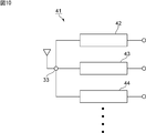
- FIG. 10 is a circuit diagram for explaining a multiplexer as a fourth embodiment of the present invention.
- band-passing filters 42, 43, 44, ... Of the first, second, third, ... are connected to the antenna terminal 33. That is, one ends of the plurality of band-passing filters 42, 43, 44, ... Are commonly connected.
- the pass bands of the band pass type filters 42, 43, 44, ... Are different from each other.
- an elastic wave filter having an elastic wave device configured according to the present invention may be used as at least one of the bandpass type filters 42, 43, 44 .... Thereby, the filter characteristics in the multiplexer 41 can be improved.
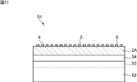
- FIG. 11 is a front sectional view showing a modified example of the elastic wave resonator used in the present invention.
- the bass velocity film 54 and the piezoelectric layer 2A are laminated on the support substrate 52. That is, a thin piezoelectric layer 2A is used instead of the piezoelectric substrate 2 shown in FIG. 1 (a).
- the bass velocity film 54 is arranged between the piezoelectric layer 2A and the support substrate 52.
- the bass velocity film 54 is made of a bass velocity material.
- the support substrate 52 is made of a hypersonic material.
- the low sound velocity material refers to a material in which the sound velocity of the propagating bulk wave is lower than the sound velocity of the bulk wave propagating in the piezoelectric layer 2A.
- the hypersonic material is a material in which the sound velocity of the propagating bulk wave is faster than the sound velocity of the elastic wave propagating in the piezoelectric layer 2A.
- an appropriate material having a bulk wave sound velocity lower than that of the bulk wave propagating in the piezoelectric layer can be used.
- Examples of such a low sound velocity material include silicon oxide, glass, silicon nitride, tantalum oxide, a compound obtained by adding fluorine, carbon, boron, hydrogen, or a silanol group to silicon oxide, and a medium containing the above material as a main component.
- Various materials such as, etc. can be used.
- high-frequency materials examples include aluminum oxide, silicon carbide, silicon nitride, silicon nitride, silicon, sapphire, lithium tantalate, lithium niobate, crystal, alumina, zirconia, cordylite, mulite, steatite, forsterite, and magnesia.
- DLC diamond-like carbon film or diamond, a medium containing the above material as a main component, a medium containing a mixture of the above materials as a main component, and the like can be used.
- the piezoelectric substrate in which the low sound velocity film 54 and the piezoelectric layer 2A are laminated on the support substrate 52 made of the high sound velocity material may be used.
- the hypersonic film 53 shown by the broken line may be laminated between the support substrate 52 and the low sound velocity film 54.
- the hypersonic film 53 is made of the above hypersonic material.
- the support substrate 52 may be made of a material other than the hypersonic material.
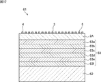
- FIG. 12 is a front sectional view showing another modified example of the structure of the elastic wave resonator.
- the acoustic multilayer film 63 is laminated between the piezoelectric layer 2A and the support substrate 62.
- the support substrate 62 is made of an appropriate insulator such as Si or a semiconductor.
- the acoustic multilayer film 63 has low acoustic impedance layers 63a, 63c, 63e having a relatively low acoustic impedance and high acoustic impedance layers 63b, 63d, 63f having a relatively high acoustic impedance.
- the low acoustic impedance layers 63a, 63c, 63e are made of a material having a relatively low acoustic impedance, such as silicon oxide.
- Silicon oxide is represented by SiO x (x is an integer).
- the value of x is not particularly limited, but in the present embodiment, each low acoustic impedance layer is made of SiO 2 .
- the material of the plurality of low acoustic impedance layers is not limited to the above, and may be any material having a relatively low acoustic impedance.
- the high acoustic impedance layers 63b, 63d, 63f may be, for example, a metal such as Pt or W, or a dielectric such as AlN or SiN.
- the material of the plurality of high acoustic impedance layers may be any material having a relatively high acoustic impedance.
- acoustic multilayer film 63 By using the acoustic multilayer film 63, it is possible to confine the excited elastic wave in the piezoelectric layer 2A.
- a piezoelectric substrate having such an acoustic multilayer film 63 may be used.
- a cavity may be used to confine the elastic wave. In this case, a cavity may be formed in the support substrate 62, and the piezoelectric layer 2A may be formed on the support substrate so as to cover the cavity.
- Low-acoustic impedance layers 63b, 63d, 63f High-acoustic impedance layers P1 to P3 ... Parallel arm resonators S1, S2, S3a, S3b ... Series arm resonator
Abstract
Provided is an elastic wave device capable of improving linearity and reducing the level of higher harmonics. This elastic wave device is provided with: an IDT electrode that is laminated on a piezoelectric substrate 2 and that constitutes a first resonator 12; and an IDT electrode that is laminated on the piezoelectric substrate 2 and that constitutes a second resonator 12. The first resonator 12 and the second resonator 13 are connected in parallel or in series, the IDT electrode of the first resonator 12 has an electrode layer comprising an epitaxial film, and the IDT electrode of the second resonator 13 has an electrode layer comprising a non-epitaxial film.
Description
本発明は、圧電体層上に互いに並列又は直列に接続されている第1の共振子及び第2の共振子が構成されている弾性波装置及び複合フィルタ装置に関する。
The present invention relates to an elastic wave device and a composite filter device in which a first resonator and a second resonator connected in parallel or in series with each other on a piezoelectric layer are configured.
従来、複数の弾性波共振子を有する帯域通過型フィルタが多く用いられている。このような弾性波共振子の一例が下記の特許文献1に開示されている。特許文献1に記載の弾性波共振子では、圧電基板上に電極が設けられている。電極は、下地電極層と下地電極層上に設けられた主電極層とを有する。この主電極層が、エピタキシャル成長した配向膜からなり、かつX線回折極点図において観察される回折パターンが複数の対称中心を有する双晶構造を有する多結晶薄膜とされている。
Conventionally, band-passing filters having a plurality of elastic wave resonators have been widely used. An example of such an elastic wave resonator is disclosed in Patent Document 1 below. In the elastic wave resonator described in Patent Document 1, an electrode is provided on the piezoelectric substrate. The electrode has a base electrode layer and a main electrode layer provided on the base electrode layer. The main electrode layer is a polycrystalline thin film composed of an epitaxially grown alignment film and having a twin structure in which the diffraction pattern observed in the X-ray diffraction pole diagram has a plurality of symmetrical centers.
特許文献1に記載の弾性波共振子では、上記電極が複数の対称中心を有する双晶構造をもつ多結晶薄膜であるため、耐ストレスマイグレーション性を高めることができ、耐電力性を高めることができるとされている。
In the elastic wave resonator described in Patent Document 1, since the electrode is a polycrystalline thin film having a twin structure having a plurality of centers of symmetry, stress migration resistance can be improved and power resistance can be improved. It is said that it can be done.
しかしながら、特許文献1に記載のような弾性波共振子を複数用いて帯域通過型フィルタを構成した場合、線形性が低下することにより、高調波のレベルが高くなり、フィルタ特性が劣化するおそれがあった。
However, when a band-passing filter is constructed by using a plurality of elastic wave resonators as described in Patent Document 1, the linearity is lowered, so that the harmonic level is raised and the filter characteristics may be deteriorated. there were.
本発明の目的は、複数の弾性波共振子を有する弾性波装置において、線形性を改善することができ、高調波のレベルを低減することができる、弾性波装置及び複合フィルタ装置を提供することにある。
An object of the present invention is to provide an elastic wave apparatus and a composite filter apparatus capable of improving linearity and reducing harmonic levels in an elastic wave apparatus having a plurality of elastic wave resonators. It is in.
本発明に係る弾性波装置は、圧電体層と、前記圧電体層上に積層されており、第1の共振子を構成しているIDT電極と、前記圧電体層上に積層されており、第2の共振子を構成しているIDT電極と、を備え、前記第1の共振子と前記第2の共振子とが並列又は直列に接続されており、前記第1の共振子の前記IDT電極が、エピタキシャル膜からなる電極層を有し、前記第2の共振子の前記IDT電極が非エピタキシャル膜からなる電極層を有する。
The elastic wave device according to the present invention is laminated on the piezoelectric layer and the piezoelectric layer, and is laminated on the IDT electrode constituting the first resonator and the piezoelectric layer. The IDT electrode constituting the second resonator is provided, and the first resonator and the second resonator are connected in parallel or in series, and the IDT of the first resonator is provided. The electrode has an electrode layer made of an epitaxial film, and the IDT electrode of the second resonator has an electrode layer made of a non-piezoelectric film.
本発明に係る複合フィルタ装置は、本発明に従って構成される弾性波装置からなる前記弾性波フィルタと、少なくとも1つの帯域通過型フィルタとを備え、前記弾性波フィルタと、少なくとも1つの他の前記帯域通過型フィルタとが、一端で共通接続されている。
The composite filter device according to the present invention includes the elastic wave filter comprising the elastic wave device configured according to the present invention, and at least one band-passing type filter, and includes the elastic wave filter and at least one other band. A pass-through filter is commonly connected at one end.
本発明に係る弾性波装置及び複合フィルタ装置では、第1,第2の共振子を有する帯域通過型フィルタを構成した場合、線形性の改善により、高調波のレベルを低減することができる。
In the elastic wave device and the composite filter device according to the present invention, when a band-passing type filter having the first and second resonators is configured, the level of harmonics can be reduced by improving the linearity.
以下、図面を参照しつつ、本発明の具体的な実施形態を説明することにより、本発明を明らかにする。
Hereinafter, the present invention will be clarified by explaining a specific embodiment of the present invention with reference to the drawings.
なお、本明細書に記載の各実施形態は、例示的なものであり、異なる実施形態間において、構成の部分的な置換または組み合わせが可能であることを指摘しておく。
It should be noted that each of the embodiments described herein is exemplary and that partial substitutions or combinations of configurations are possible between different embodiments.
図1(a)は、本発明の第1の実施形態の弾性波装置で用いられる弾性波共振子を説明するための正面断面図であり、図1(b)はその電極の部分拡大断面図であり、図2は電極構造を示す模式的平面図である。
FIG. 1A is a front sectional view for explaining an elastic wave resonator used in the elastic wave apparatus of the first embodiment of the present invention, and FIG. 1B is a partially enlarged sectional view of the electrode. FIG. 2 is a schematic plan view showing an electrode structure.
弾性波共振子1は、圧電体層としての圧電基板2を有する。圧電基板2は、LiTaO3からなる。圧電基板2はLiNbO3などの他の圧電単結晶からなるものであってもよい。圧電基板2上に、電極として、IDT電極3及び反射器4,5が設けられている。それによって、1ポート型弾性波共振子が構成されている。
The elastic wave resonator 1 has a piezoelectric substrate 2 as a piezoelectric layer. The piezoelectric substrate 2 is made of LiTaO 3 . The piezoelectric substrate 2 may be made of another piezoelectric single crystal such as LiNbO 3. An IDT electrode 3 and reflectors 4 and 5 are provided as electrodes on the piezoelectric substrate 2. As a result, a 1-port elastic wave resonator is formed.
IDT電極3は、互いに間挿し合う、第1,第2の電極指3a,3bを有する。図1(b)は、第1の電極指3aが設けられている部分の部分拡大断面図である。第1の電極指3aでは、圧電基板2上に下地電極層6及び主電極層7が積層されている。下地電極層6は、Tiからなり、主電極層7はAlからなる。なお、主電極層とは、IDT電極において弾性波を励振する上での役割を担う電極層である。主電極層は、主電極層を含む積層構造からなる場合、積層構造中において、50重量%以上の割合を占める。
The IDT electrode 3 has first and second electrode fingers 3a and 3b that are interleaved with each other. FIG. 1B is a partially enlarged cross-sectional view of a portion where the first electrode finger 3a is provided. In the first electrode finger 3a, the base electrode layer 6 and the main electrode layer 7 are laminated on the piezoelectric substrate 2. The base electrode layer 6 is made of Ti, and the main electrode layer 7 is made of Al. The main electrode layer is an electrode layer that plays a role in exciting elastic waves in the IDT electrode. When the main electrode layer has a laminated structure including the main electrode layer, the main electrode layer occupies a ratio of 50% by weight or more in the laminated structure.
下地電極層6は、Ti以外の主電極層よりも圧電基板2に対する密着性に優れた様々な金属材料により構成することができる。例えば、NiCrなどを用いてもよい。
The base electrode layer 6 can be made of various metal materials having better adhesion to the piezoelectric substrate 2 than the main electrode layer other than Ti. For example, NiCr or the like may be used.
主電極層7は、本実施形態では、Alからなるが、他の金属、例えば、Cu、Au、Ag、Pt、Mo、またはWからなるものであってもよい。また、主電極層7は、Alや上記金属を主とする合金であってもよい。
The main electrode layer 7 is made of Al in this embodiment, but may be made of another metal such as Cu, Au, Ag, Pt, Mo, or W. Further, the main electrode layer 7 may be an alloy mainly composed of Al or the above metal.
さらに、上記主電極層と下地電極層との間、また、上記主電極層の上に、少なくとも1層の他の金属層が設けられていてもよい。
Further, at least one other metal layer may be provided between the main electrode layer and the base electrode layer, and on the main electrode layer.
図3は、本発明の第1の実施形態に係る弾性波装置の略図的回路図である。弾性波装置11では、第1の共振子12と第2の共振子13とが並列接続されている。第1の共振子12及び第2の共振子13は、上記1ポート型弾性波共振子からなる。
FIG. 3 is a schematic circuit diagram of an elastic wave device according to the first embodiment of the present invention. In the elastic wave device 11, the first resonator 12 and the second resonator 13 are connected in parallel. The first resonator 12 and the second resonator 13 are composed of the above-mentioned 1-port elastic wave resonator.
弾性波装置11の特徴は、第1の共振子12におけるIDT電極の主電極層がエピタキシャル膜からなり、第2の共振子13のIDT電極が、非エピタキシャル膜からなる主電極層を有することにある。それによって、弾性波装置11では、線形性が改善され、帯域通過型フィルタを構成した場合の高調波のレベルを抑制することができる。
The feature of the elastic wave device 11 is that the main electrode layer of the IDT electrode in the first resonator 12 is made of an epitaxial film, and the IDT electrode of the second resonator 13 has a main electrode layer made of a non-epitaxial film. be. As a result, in the elastic wave device 11, the linearity is improved, and the level of harmonics when the band-passing type filter is configured can be suppressed.
ここで、エピタキシャル膜とは、主電極層7の結晶面(例えばAlの場合は(111)面)の法線が圧電基板2のc軸とほぼ一致し、X線回折極点図(XRD極点図)において観察される回折パターンが、6回対称のスポットを有する、単結晶膜である。図4は、第1の実施形態における、Alからなる主電極層のXRD極点図を示す。図4から明らかなように、6回対称スポットが現れている。
Here, in the epitaxial film, the normal line of the crystal plane (for example, the (111) plane in the case of Al) of the main electrode layer 7 substantially coincides with the c-axis of the piezoelectric substrate 2, and the X-ray diffraction pole point diagram (XRD pole point diagram). ) Is a single crystal film having 6-fold symmetrical spots. FIG. 4 shows an XRD pole figure of the main electrode layer made of Al in the first embodiment. As is clear from FIG. 4, 6-fold symmetric spots appear.
本発明では、第1の共振子が上記のように、このようなエピタキシャル膜からなる主電極層を有する。
In the present invention, the first resonator has a main electrode layer made of such an epitaxial film as described above.
他方、図5は、Alからなる主電極層が非エピタキシャル膜である場合のXRD極点図である。非エピタキシャル膜は、6回対称スポットが現れない回折パターンを示す。
On the other hand, FIG. 5 is an XRD pole figure when the main electrode layer made of Al is a non-epitaxial film. The non-epitaxial film shows a diffraction pattern in which 6-fold symmetric spots do not appear.
本発明では、上記のように第2の共振子のIDT電極が、非エピタキシャル膜である主電極層を有する。
In the present invention, as described above, the IDT electrode of the second resonator has a main electrode layer which is a non-epitaxial film.
第1の共振子と第2の共振子とは、主電極層が上記のように異なるため、高調波の周波数依存性が異なる。図6は、第1の共振子と第2の共振子の周波数と、三次高調波レベルとの関係を示す図である。実線が第1の共振子についての関係を、破線が第2の共振子についての関係を示す。ここで、弾性波共振子1は、42度カットLiTaO3からなる圧電基板2上に、厚み30nmのTi膜からなる下地電極層6と、厚み415nmのAl膜からなる主電極層7を積層した構造とした。第1の共振子では、Al膜がエピタキシャル膜であり、第2の共振子では、Al膜が非エピタキシャル膜とされている。
Since the main electrode layer of the first resonator and the second resonator are different as described above, the frequency dependence of the harmonics is different. FIG. 6 is a diagram showing the relationship between the frequencies of the first resonator and the second resonator and the third harmonic level. The solid line shows the relationship for the first resonator, and the broken line shows the relationship for the second resonator. Here, the elastic wave resonator 1 is formed by laminating a base electrode layer 6 made of a Ti film having a thickness of 30 nm and a main electrode layer 7 made of an Al film having a thickness of 415 nm on a piezoelectric substrate 2 made of a 42-degree cut LiTaO 3. The structure was used. In the first resonator, the Al film is an epitaxial film, and in the second resonator, the Al film is a non-epitaxial film.
なお、上記エピタキシャル膜の成膜については、例えば特開2002-305402号公報に記載の方法により行うことができる。すなわち、圧電基板にイオンエッチングにより前処理を行ったのちに、Tiからなる下地電極層を成膜する。次に、Alからなる主電極層を、形成する。この場合、Alの結晶の(111)面が圧電基板におけるLiTaO3のc軸に垂直となるように、Alをエピタキシャル成長させる。
The film formation of the epitaxial film can be carried out by, for example, the method described in JP-A-2002-305402. That is, after the piezoelectric substrate is pretreated by ion etching, a base electrode layer made of Ti is formed. Next, a main electrode layer made of Al is formed. In this case, Al is epitaxially grown so that the (111) plane of the Al crystal is perpendicular to the c-axis of LiTaO 3 on the piezoelectric substrate.
他方、第2の共振子の非エピタキシャル膜については、上記イオンエッチングによる処理を行わずに、下地電極層であるTi膜及び主電極層であるAl膜を成膜することにより得られる。
On the other hand, the non-epitaxial film of the second resonator can be obtained by forming a Ti film as a base electrode layer and an Al film as a main electrode layer without performing the above-mentioned ion etching treatment.
もっとも、エピタキシャル膜からなる主電極層及び非エピタキシャル膜からなる主電極層の形成方法は特に限定されるものではない。
However, the method of forming the main electrode layer made of an epitaxial film and the main electrode layer made of a non-epitaxial film is not particularly limited.
図6から明らかなように、エピタキシャル膜を有する第1の共振子と、非エピタキシャル膜を有する第2の共振子とでは、三次高調波のレベル(H3レベル)の周波数依存性が大きく異なっていることがわかる。
As is clear from FIG. 6, the frequency dependence of the third harmonic level (H3 level) is significantly different between the first resonator having an epitaxial film and the second resonator having a non-epitaxial film. You can see that.
図7は、第1の実施形態に係る弾性波装置についての実施例1と、以下の比較例1及び比較例2の各弾性波装置の周波数と、三次高調波のレベル(H3レベル)との関係を示す図である。実線が実施例1、破線が比較例1、一点鎖線が比較例2の結果を示す。
FIG. 7 shows the frequency of each elastic wave device of Example 1 and the following Comparative Examples 1 and 2 for the elastic wave device according to the first embodiment, and the level of the third harmonic (H3 level). It is a figure which shows the relationship. The solid line shows the result of Example 1, the broken line shows the result of Comparative Example 1, and the alternate long and short dash line shows the result of Comparative Example 2.
実施例1では、図3に示したように第1の共振子12と第2の共振子13とが並列に接続されている。
In the first embodiment, as shown in FIG. 3, the first resonator 12 and the second resonator 13 are connected in parallel.
比較例1:第1の共振子2個が並列接続されている。
Comparative example 1: Two first resonators are connected in parallel.
比較例2:第2の共振子2個が並列接続されている。
Comparative example 2: Two second resonators are connected in parallel.
図7から明らかなように、比較例1及び比較例2に対し、第1の共振子と第2の共振子とが並列に接続されている実施例1によれば、2.5GHz以上、2.6GHz以下の範囲で、三次高調波の信号強度が5dBm~10dBm程度と格段小さくなっていることがわかる。これは、第1の共振子と第2の共振子とで、三次高調波の周波数依存性が異なるため、2.5GHz以上、2.6GHz以下の周波数帯において、三次高調波の信号が相殺されているためと考えられる。
As is clear from FIG. 7, according to Example 1 in which the first resonator and the second resonator are connected in parallel with respect to Comparative Example 1 and Comparative Example 2, 2.5 GHz or more, 2 It can be seen that the signal intensity of the third harmonic is remarkably small, about 5 dBm to 10 dBm, in the range of .6 GHz or less. This is because the frequency dependence of the third harmonic differs between the first resonator and the second resonator, so that the signal of the third harmonic is canceled in the frequency band of 2.5 GHz or more and 2.6 GHz or less. It is thought that this is because.
図8は、本発明の第2の実施形態に係る弾性波装置の略図的回路図である。弾性波装置21では、第1の共振子12と第2の共振子13とが直列に接続されている。本発明では、第1の共振子12と第2の共振子13は並列に接続されていてもよく、直列に接続されていてもよい。
FIG. 8 is a schematic circuit diagram of an elastic wave device according to a second embodiment of the present invention. In the elastic wave device 21, the first resonator 12 and the second resonator 13 are connected in series. In the present invention, the first resonator 12 and the second resonator 13 may be connected in parallel or may be connected in series.
また、図3に破線で示すように、少なくとも1つの第3の共振子Xがさらに並列に接続されていてもよく、弾性波装置21においても、少なくとも1つの弾性波共振子が直列にさらに接続されていてもよい。
Further, as shown by a broken line in FIG. 3, at least one third resonator X may be further connected in parallel, and in the elastic wave device 21, at least one elastic wave resonator is further connected in series. It may have been done.
図9は、本発明の第3の実施形態としてのラダー型フィルタ31の回路図である。ラダー型フィルタ31は、送信フィルタである。
FIG. 9 is a circuit diagram of a ladder type filter 31 as a third embodiment of the present invention. The ladder type filter 31 is a transmission filter.
ラダー型フィルタ31では、入力端子32とアンテナ端子33との間に複数の弾性波共振子が接続されている。すなわち、入力端子32とアンテナ端子33とを結ぶ直列腕に、直列腕共振子S1,S2,S3a,S3bが設けられている。また、直列腕とグラウンド電位とを結ぶ複数の並列腕において、それぞれ、並列腕共振子P1,P2,P3が配置されている。これらの直列腕共振子S1,S2,S3a,S3b及び並列腕共振子P1,P2,P3は、いずれも弾性波共振子からなる。
In the ladder type filter 31, a plurality of elastic wave resonators are connected between the input terminal 32 and the antenna terminal 33. That is, the series arm resonators S1, S2, S3a, and S3b are provided on the series arm connecting the input terminal 32 and the antenna terminal 33. Further, parallel arm resonators P1, P2, and P3 are arranged in a plurality of parallel arms connecting the series arm and the ground potential, respectively. These series arm resonators S1, S2, S3a, S3b and parallel arm resonators P1, P2, P3 are all made of elastic wave resonators.
そして、直列腕共振子S3aと直列腕共振子S3bとは1つの弾性波共振子を並列分割した分割タイプの弾性波共振子である。具体的には、直列腕共振子S3aと直列腕共振子S3bとは、1つの直列腕共振子が並列分割された並列分割タイプの共振子であり、入力端子32とアンテナ端子33とを結ぶ経路上の接続ノードにおいて互いに並列に接続された弾性波共振子である。ここで、分割タイプの弾性波共振子とは分割前の弾性波共振子のインピーダンスとほぼ同じインピーダンスとなるように、並列または直列に接続されている形式の弾性波共振子である。すなわち、分割タイプの弾性波共振子の総静電容量は、分割前の弾性波共振子の静電容量とほぼ等しくなる。なお、直列腕共振子S3aと直列腕共振子S3bとが、1つの直列腕共振子を直列分割した直列分割タイプの共振子であった場合、直列腕共振子S3aと直列腕共振子S3bとは入力端子32とアンテナ端子33とを結ぶ経路上において互いに直列に接続され、互いの間にはいずれの並列腕共振子も接続されることがない。
The series arm resonator S3a and the series arm resonator S3b are split type elastic wave resonators in which one elastic wave resonator is divided in parallel. Specifically, the series arm resonator S3a and the series arm resonator S3b are parallel division type resonators in which one series arm resonator is divided in parallel, and a path connecting the input terminal 32 and the antenna terminal 33. Elastic wave resonators connected in parallel with each other at the above connection node. Here, the split type elastic wave resonator is a type of elastic wave resonator connected in parallel or in series so as to have substantially the same impedance as the impedance of the elastic wave resonator before division. That is, the total capacitance of the split type elastic wave resonator is substantially equal to the capacitance of the elastic wave resonator before splitting. When the series arm resonator S3a and the series arm resonator S3b are series division type resonators in which one series arm resonator is divided in series, the series arm resonator S3a and the series arm resonator S3b are different from each other. They are connected in series with each other on the path connecting the input terminal 32 and the antenna terminal 33, and none of the parallel arm resonators are connected between them.
なお、並列腕共振子P1~P3のうちいずれかの並列腕共振子が分割タイプの弾性波共振子であってもよい。その場合、入力端子32とアンテナ端子33とを結ぶ経路において当該いずれかの並列腕共振子が接続される接続ノードとグラウンド電位とを結ぶ経路において、分割タイプの弾性波共振子同士が互いに並列または直列に接続されている。
Note that any of the parallel arm resonators P1 to P3 may be a split type elastic wave resonator. In that case, in the path connecting the input terminal 32 and the antenna terminal 33, in the path connecting the connection node to which the parallel arm resonator is connected and the ground potential, the split type elastic wave resonators are parallel to each other or are connected to each other. They are connected in series.
本第3の実施形態では、直列腕共振子S3aが本発明における第1の共振子からなり、直列腕共振子S3bが本発明における第2の共振子からなる。
In the third embodiment, the series arm resonator S3a is composed of the first resonator in the present invention, and the series arm resonator S3b is composed of the second resonator in the present invention.
ラダー型フィルタ31では、直列腕共振子S3a,S3bが、1つの直列腕共振子を2分割した分割タイプの弾性波共振子であり、本発明に従って構成されているため、線形性を高めることができる。従って、ラダー型フィルタ31では、高調波のレベルを効果的に抑制でき、良好なフィルタ特性を得ることができる。
In the ladder type filter 31, the series arm resonators S3a and S3b are divided type elastic wave resonators in which one series arm resonator is divided into two, and are configured according to the present invention, so that the linearity can be improved. can. Therefore, in the ladder type filter 31, the level of harmonics can be effectively suppressed, and good filter characteristics can be obtained.
また、ラダー型フィルタ31では、アンテナ端子33に最も近い共振子が、フィルタ特性に大きな影響を与える。従って、上記本発明に従って構成された弾性波装置を構成している直列腕共振子S3a及び直列腕共振子S3bがアンテナ端子33に最も近い弾性波共振子であることが好ましい。
Further, in the ladder type filter 31, the resonator closest to the antenna terminal 33 has a great influence on the filter characteristics. Therefore, it is preferable that the series arm resonator S3a and the series arm resonator S3b constituting the elastic wave device configured according to the present invention are elastic wave resonators closest to the antenna terminal 33.
なお、図9ではラダー型フィルタ31を示したが、本発明の弾性波装置は、ラダー型フィルタ以外の複数の弾性波共振子を有するフィルタに広く適用することができる。また、図9では、並列接続されている分割タイプの直列腕共振子S3a,S3bを示したが、例えば、直列腕共振子S2が第1,第2の共振子に直列分割されていてもよい。
Although the ladder type filter 31 is shown in FIG. 9, the elastic wave device of the present invention can be widely applied to a filter having a plurality of elastic wave resonators other than the ladder type filter. Further, in FIG. 9, the split type series arm resonators S3a and S3b connected in parallel are shown. For example, the series arm resonator S2 may be split in series with the first and second resonators. ..
さらに、例えば、直列腕共振子S2が第1の共振子からなり、並列腕共振子P3が第2の共振子からなるものであってもよい。すなわち、互いに接続されている直列腕共振子と並列腕共振子の一方が第1の共振子であり、他方が第2の共振子であってもよい。その場合においても、本発明に従って、線形性の改善により高調波のレベルを効果的に小さくすることができる。
Further, for example, the series arm resonator S2 may be composed of the first resonator, and the parallel arm resonator P3 may be composed of the second resonator. That is, one of the series arm resonator and the parallel arm resonator connected to each other may be the first resonator and the other may be the second resonator. Even in that case, according to the present invention, the level of harmonics can be effectively reduced by improving the linearity.
図10は、本発明の第4の実施形態としてのマルチプレクサを説明するための回路図である。マルチプレクサ41では、アンテナ端子33に第1,第2,第3,……の帯域通過型フィルタ42,43,44,……が接続されている。すなわち、複数の帯域通過型フィルタ42,43,44,……の一端が共通接続されている。帯域通過型フィルタ42,43,44,……の通過帯域は互いに異なっている。
FIG. 10 is a circuit diagram for explaining a multiplexer as a fourth embodiment of the present invention. In the multiplexer 41, band-passing filters 42, 43, 44, ... Of the first, second, third, ... Are connected to the antenna terminal 33. That is, one ends of the plurality of band-passing filters 42, 43, 44, ... Are commonly connected. The pass bands of the band pass type filters 42, 43, 44, ... Are different from each other.
このマルチプレクサ41において、帯域通過型フィルタ42,43,44……の少なくとも1つとして、本発明に従って構成された弾性波装置を有する弾性波フィルタを用いてもよい。それによって、マルチプレクサ41におけるフィルタ特性の改善を図ることができる。
In this multiplexer 41, an elastic wave filter having an elastic wave device configured according to the present invention may be used as at least one of the bandpass type filters 42, 43, 44 .... Thereby, the filter characteristics in the multiplexer 41 can be improved.
図11は、本発明で用いられる弾性波共振子の変形例を示す正面断面図である。弾性波共振子51では、支持基板52上に、低音速膜54及び圧電層2Aが積層されている。すなわち、図1(a)に示した圧電基板2に代えて、薄い圧電層2Aが用いられている。そして、圧電層2Aと、支持基板52との間に、低音速膜54が配置されている。低音速膜54は、低音速材料からなる。支持基板52は、高音速材料からなる。低音速材料とは、伝搬するバルク波の音速が、圧電層2Aを伝搬するバルク波の音速よりも低い材料をいう。高音速材料とは、伝搬するバルク波の音速が圧電層2Aを伝搬する弾性波の音速よりも速い材料をいう。
FIG. 11 is a front sectional view showing a modified example of the elastic wave resonator used in the present invention. In the elastic wave resonator 51, the bass velocity film 54 and the piezoelectric layer 2A are laminated on the support substrate 52. That is, a thin piezoelectric layer 2A is used instead of the piezoelectric substrate 2 shown in FIG. 1 (a). Then, the bass velocity film 54 is arranged between the piezoelectric layer 2A and the support substrate 52. The bass velocity film 54 is made of a bass velocity material. The support substrate 52 is made of a hypersonic material. The low sound velocity material refers to a material in which the sound velocity of the propagating bulk wave is lower than the sound velocity of the bulk wave propagating in the piezoelectric layer 2A. The hypersonic material is a material in which the sound velocity of the propagating bulk wave is faster than the sound velocity of the elastic wave propagating in the piezoelectric layer 2A.
上記低音速材料としては、圧電層を伝搬するバルク波よりも低音速のバルク波音速を有する適宜の材料を用いることができる。このような低音速材料としては、酸化ケイ素、ガラス、酸窒化ケイ素、酸化タンタル、また、酸化ケイ素にフッ素や炭素やホウ素、水素、あるいはシラノール基を加えた化合物、上記材料を主成分とする媒質等の様々な材料を用いることができる。
As the bass sound material, an appropriate material having a bulk wave sound velocity lower than that of the bulk wave propagating in the piezoelectric layer can be used. Examples of such a low sound velocity material include silicon oxide, glass, silicon nitride, tantalum oxide, a compound obtained by adding fluorine, carbon, boron, hydrogen, or a silanol group to silicon oxide, and a medium containing the above material as a main component. Various materials such as, etc. can be used.
上記高音速材料としては、酸化アルミニウム、炭化ケイ素、窒化ケイ素、酸窒化ケイ素、シリコン、サファイア、タンタル酸リチウム、ニオブ酸リチウム、水晶、アルミナ、ジルコニア、コージライト、ムライト、ステアタイト、フォルステライト、マグネシア、DLC(ダイヤモンドライクカーボン)膜またはダイヤモンド、上記材料を主成分とする媒質、上記材料の混合物を主成分とする媒質等の様々な材料を用いることができる。
Examples of the high-frequency materials include aluminum oxide, silicon carbide, silicon nitride, silicon nitride, silicon, sapphire, lithium tantalate, lithium niobate, crystal, alumina, zirconia, cordylite, mulite, steatite, forsterite, and magnesia. , DLC (diamond-like carbon) film or diamond, a medium containing the above material as a main component, a medium containing a mixture of the above materials as a main component, and the like can be used.
このように、高音速材料からなる支持基板52上に低音速膜54及び圧電層2Aを積層した圧電基板を用いてもよい。また、破線で示す高音速膜53を、支持基板52と低音速膜54との間に積層してもよい。高音速膜53は上記高音速材料からなる。その場合、支持基板52は高音速材料以外の材料からなるものであってもよい。
As described above, the piezoelectric substrate in which the low sound velocity film 54 and the piezoelectric layer 2A are laminated on the support substrate 52 made of the high sound velocity material may be used. Further, the hypersonic film 53 shown by the broken line may be laminated between the support substrate 52 and the low sound velocity film 54. The hypersonic film 53 is made of the above hypersonic material. In that case, the support substrate 52 may be made of a material other than the hypersonic material.
図12は、弾性波共振子の構造の他の変形例を示す正面断面図である。弾性波共振子61では、圧電層2Aと支持基板62との間に音響多層膜63が積層されている。支持基板62は、Siなどの適宜の絶縁体もしくは半導体からなる。
FIG. 12 is a front sectional view showing another modified example of the structure of the elastic wave resonator. In the elastic wave resonator 61, the acoustic multilayer film 63 is laminated between the piezoelectric layer 2A and the support substrate 62. The support substrate 62 is made of an appropriate insulator such as Si or a semiconductor.
音響多層膜63は、相対的に音響インピーダンスが低い低音響インピーダンス層63a,63c,63eと、相対的に音響インピーダンスが高い高音響インピーダンス層63b,63d,63fとを有する。
The acoustic multilayer film 63 has low acoustic impedance layers 63a, 63c, 63e having a relatively low acoustic impedance and high acoustic impedance layers 63b, 63d, 63f having a relatively high acoustic impedance.
低音響インピーダンス層63a,63c,63eは、例えば、酸化ケイ素などの相対的に音響インピーダンスが低い材料からなる。酸化ケイ素はSiOx(xは整数)により表される。xの値は特に限定されないが、本実施形態においては、各低音響インピーダンス層はSiO2からなる。なお、上記複数の低音響インピーダンス層の材料は上記に限定されず、相対的に音響インピーダンスが低い材料であればよい。
The low acoustic impedance layers 63a, 63c, 63e are made of a material having a relatively low acoustic impedance, such as silicon oxide. Silicon oxide is represented by SiO x (x is an integer). The value of x is not particularly limited, but in the present embodiment, each low acoustic impedance layer is made of SiO 2 . The material of the plurality of low acoustic impedance layers is not limited to the above, and may be any material having a relatively low acoustic impedance.
高音響インピーダンス層63b,63d,63fは、例えば、PtまたはWなどの金属や、AlNまたはSiNなどの誘電体であってもよい。複数の高音響インピーダンス層の材料は、相対的に音響インピーダンスが高い材料であればよい。
The high acoustic impedance layers 63b, 63d, 63f may be, for example, a metal such as Pt or W, or a dielectric such as AlN or SiN. The material of the plurality of high acoustic impedance layers may be any material having a relatively high acoustic impedance.
音響多層膜63を用いることにより、圧電層2A内に励振された弾性波を閉じ込めることができる。このような音響多層膜63を有する圧電基板を用いてもよい。なお、音響多層膜63の代わりに、空洞部を用いて弾性波を閉じ込めてもよい。この場合、支持基板62に空洞部を形成し、その空洞部を覆うように圧電層2Aを支持基板上に形成すればよい。
By using the acoustic multilayer film 63, it is possible to confine the excited elastic wave in the piezoelectric layer 2A. A piezoelectric substrate having such an acoustic multilayer film 63 may be used. Instead of the acoustic multilayer film 63, a cavity may be used to confine the elastic wave. In this case, a cavity may be formed in the support substrate 62, and the piezoelectric layer 2A may be formed on the support substrate so as to cover the cavity.
1,51,61…弾性波共振子
2…圧電基板
2A…圧電層
3…IDT電極
3a,3b…第1,第2の電極指
4,5…反射器
6…下地電極層
7…主電極層
11,21…弾性波装置
12,13…第1,第2の共振子
31…ラダー型フィルタ
32…入力端子
33…アンテナ端子
41…マルチプレクサ
42~44…帯域通過型フィルタ
52,62…支持基板
53…高音速膜
54…低音速膜
63…音響多層膜
63a,63c,63e…低音響インピーダンス層
63b,63d,63f…高音響インピーダンス層
P1~P3…並列腕共振子
S1,S2,S3a,S3b…直列腕共振子 1,51,61 ...Elastic wave resonator 2 ... piezoelectric substrate 2A ... piezoelectric layer 3 ... IDT electrodes 3a, 3b ... first and second electrode fingers 4, 5 ... reflector 6 ... base electrode layer 7 ... main electrode layer 11,21 ... Elastic wave devices 12, 13 ... First and second resonators 31 ... Ladder type filter 32 ... Input terminal 33 ... Antenna terminal 41 ... multiplexer 42 to 44 ... Band-passing type filters 52, 62 ... Support substrate 53 ... High-pitched speed film 54 ... Low-pitched speed film 63 ... Acoustic multilayer film 63a, 63c, 63e ... Low- acoustic impedance layers 63b, 63d, 63f ... High-acoustic impedance layers P1 to P3 ... Parallel arm resonators S1, S2, S3a, S3b ... Series arm resonator
2…圧電基板
2A…圧電層
3…IDT電極
3a,3b…第1,第2の電極指
4,5…反射器
6…下地電極層
7…主電極層
11,21…弾性波装置
12,13…第1,第2の共振子
31…ラダー型フィルタ
32…入力端子
33…アンテナ端子
41…マルチプレクサ
42~44…帯域通過型フィルタ
52,62…支持基板
53…高音速膜
54…低音速膜
63…音響多層膜
63a,63c,63e…低音響インピーダンス層
63b,63d,63f…高音響インピーダンス層
P1~P3…並列腕共振子
S1,S2,S3a,S3b…直列腕共振子 1,51,61 ...
Claims (11)
- 圧電基板と、
前記圧電体層上に積層されており、第1の共振子を構成しているIDT電極と、
前記圧電体層上に積層されており、第2の共振子を構成しているIDT電極と、
を備え、
前記第1の共振子と前記第2の共振子とが並列又は直列に接続されており、
前記第1の共振子の前記IDT電極が、エピタキシャル膜からなる電極層を有し、前記第2の共振子の前記IDT電極が非エピタキシャル膜からなる電極層を有する、弾性波装置。 Piezoelectric board and
The IDT electrode, which is laminated on the piezoelectric layer and constitutes the first resonator,
The IDT electrode, which is laminated on the piezoelectric layer and constitutes the second resonator,
With
The first resonator and the second resonator are connected in parallel or in series.
An elastic wave device in which the IDT electrode of the first resonator has an electrode layer made of an epitaxial film, and the IDT electrode of the second resonator has an electrode layer made of a non-epitaxial film. - IDT電極が下地電極層と主電極層の積層構造を有する、請求項1に記載の弾性波装置。 The elastic wave device according to claim 1, wherein the IDT electrode has a laminated structure of a base electrode layer and a main electrode layer.
- 前記第1の共振子及び前記第2の共振子は、分割前とインピーダンスが同等となるように1つの共振子を分割した分割タイプの複数の共振子である、請求項1または2に記載の弾性波装置。 The first or second resonator according to claim 1 or 2, wherein the first resonator and the second resonator are a plurality of division type resonators in which one resonator is divided so that the impedance is the same as that before the division. Elastic wave device.
- 前記第1,第2の共振子が、並列分割タイプの各共振子である、請求項3に記載の弾性波装置。 The elastic wave device according to claim 3, wherein the first and second resonators are each resonator of the parallel division type.
- 前記第1,第2の共振子が、直列分割タイプの各共振子である、請求項3に記載の弾性波装置。 The elastic wave device according to claim 3, wherein the first and second resonators are each resonator of the series division type.
- 弾性波フィルタである、請求項1~5のいずれか1項に記載の弾性波装置。 The elastic wave device according to any one of claims 1 to 5, which is an elastic wave filter.
- 前記弾性波フィルタが、アンテナ端子と、前記第1の共振子及び前記第2の共振子を含む複数の共振子を有する、請求項6に記載の弾性波装置。 The elastic wave device according to claim 6, wherein the elastic wave filter has an antenna terminal and a plurality of resonators including the first resonator and the second resonator.
- 前記第1の共振子及び前記第2の共振子が、前記複数の共振子の内、前記アンテナ端子に最も近い共振子である、請求項7に記載の弾性波装置。 The elastic wave device according to claim 7, wherein the first resonator and the second resonator are the resonator closest to the antenna terminal among the plurality of resonators.
- 送信フィルタである、請求項6~8のいずれか1項に記載の弾性波装置。 The elastic wave device according to any one of claims 6 to 8, which is a transmission filter.
- 請求項6~9のいずれか1項に記載の弾性波装置からなる前記弾性波フィルタと、少なくとも1つの帯域通過型フィルタとを備え、前記弾性波フィルタと、少なくとも1つの他の前記帯域通過型フィルタとが、一端で共通接続されている、複合フィルタ装置。 The elastic wave filter comprising the elastic wave device according to any one of claims 6 to 9 and at least one band-passing type filter, and the elastic wave filter and at least one other band-passing type. A compound filter device in which a filter is commonly connected at one end.
- マルチプレクサである、請求項10に記載の複合フィルタ装置。 The composite filter device according to claim 10, which is a multiplexer.
Priority Applications (3)
| Application Number | Priority Date | Filing Date | Title |
|---|---|---|---|
| CN202180017643.5A CN115191084A (en) | 2020-03-18 | 2021-03-08 | Elastic wave device and composite filter device |
| JP2022508227A JP7428237B2 (en) | 2020-03-18 | 2021-03-08 | Elastic wave device and composite filter device |
| US17/903,296 US20220416764A1 (en) | 2020-03-18 | 2022-09-06 | Acoustic wave device and composite filter device |
Applications Claiming Priority (2)
| Application Number | Priority Date | Filing Date | Title |
|---|---|---|---|
| JP2020-047272 | 2020-03-18 | ||
| JP2020047272 | 2020-03-18 |
Related Child Applications (1)
| Application Number | Title | Priority Date | Filing Date |
|---|---|---|---|
| US17/903,296 Continuation US20220416764A1 (en) | 2020-03-18 | 2022-09-06 | Acoustic wave device and composite filter device |
Publications (1)
| Publication Number | Publication Date |
|---|---|
| WO2021187200A1 true WO2021187200A1 (en) | 2021-09-23 |
Family
ID=77771257
Family Applications (1)
| Application Number | Title | Priority Date | Filing Date |
|---|---|---|---|
| PCT/JP2021/009028 WO2021187200A1 (en) | 2020-03-18 | 2021-03-08 | Elastic wave device and composite filter device |
Country Status (4)
| Country | Link |
|---|---|
| US (1) | US20220416764A1 (en) |
| JP (1) | JP7428237B2 (en) |
| CN (1) | CN115191084A (en) |
| WO (1) | WO2021187200A1 (en) |
Citations (7)
| Publication number | Priority date | Publication date | Assignee | Title |
|---|---|---|---|---|
| JP2000349591A (en) * | 1999-06-08 | 2000-12-15 | Oki Electric Ind Co Ltd | Branching filter using surface acoustic wave filter |
| WO2009063559A1 (en) * | 2007-11-15 | 2009-05-22 | Fujitsu Limited | Elastic wave device, duplexer using the same, and communication apparatus using the duplexer |
| WO2009150786A1 (en) * | 2008-06-09 | 2009-12-17 | 株式会社村田製作所 | Elastic surface wave device, and manufacturing method therefor |
| JP2011097237A (en) * | 2009-10-28 | 2011-05-12 | Kyocera Corp | Surface acoustic wave device |
| JP2011211460A (en) * | 2010-03-30 | 2011-10-20 | Sae Magnetics (Hk) Ltd | Surface acoustic wave device |
| JP2018157510A (en) * | 2017-03-21 | 2018-10-04 | 太陽誘電株式会社 | Multiplexer |
| WO2019111902A1 (en) * | 2017-12-06 | 2019-06-13 | 株式会社村田製作所 | Multiplexer, high-frequency front-end circuit, and communication device |
-
2021
- 2021-03-08 CN CN202180017643.5A patent/CN115191084A/en active Pending
- 2021-03-08 WO PCT/JP2021/009028 patent/WO2021187200A1/en active Application Filing
- 2021-03-08 JP JP2022508227A patent/JP7428237B2/en active Active
-
2022
- 2022-09-06 US US17/903,296 patent/US20220416764A1/en active Pending
Patent Citations (7)
| Publication number | Priority date | Publication date | Assignee | Title |
|---|---|---|---|---|
| JP2000349591A (en) * | 1999-06-08 | 2000-12-15 | Oki Electric Ind Co Ltd | Branching filter using surface acoustic wave filter |
| WO2009063559A1 (en) * | 2007-11-15 | 2009-05-22 | Fujitsu Limited | Elastic wave device, duplexer using the same, and communication apparatus using the duplexer |
| WO2009150786A1 (en) * | 2008-06-09 | 2009-12-17 | 株式会社村田製作所 | Elastic surface wave device, and manufacturing method therefor |
| JP2011097237A (en) * | 2009-10-28 | 2011-05-12 | Kyocera Corp | Surface acoustic wave device |
| JP2011211460A (en) * | 2010-03-30 | 2011-10-20 | Sae Magnetics (Hk) Ltd | Surface acoustic wave device |
| JP2018157510A (en) * | 2017-03-21 | 2018-10-04 | 太陽誘電株式会社 | Multiplexer |
| WO2019111902A1 (en) * | 2017-12-06 | 2019-06-13 | 株式会社村田製作所 | Multiplexer, high-frequency front-end circuit, and communication device |
Also Published As
| Publication number | Publication date |
|---|---|
| CN115191084A (en) | 2022-10-14 |
| JPWO2021187200A1 (en) | 2021-09-23 |
| JP7428237B2 (en) | 2024-02-06 |
| US20220416764A1 (en) | 2022-12-29 |
Similar Documents
| Publication | Publication Date | Title |
|---|---|---|
| CN111587535B (en) | Elastic wave device, multiplexer, high frequency front-end circuit, and communication device | |
| JP4419961B2 (en) | Boundary acoustic wave device | |
| JP4552931B2 (en) | Elastic wave device, mobile communication device and sensor using the same | |
| WO2018164209A1 (en) | Acoustic wave device, acoustic wave device package, high-frequency front-end circuit, and communication device | |
| WO2018216417A1 (en) | Elastic wave device, filter, high-frequency front-end circuit and communication apparatus | |
| WO2021039639A1 (en) | Elastic wave device | |
| US20200389147A1 (en) | Acoustic wave device | |
| WO2020261763A1 (en) | Elastic wave device | |
| CN113454912B (en) | Elastic wave device | |
| JPWO2020209190A1 (en) | Elastic wave device and multiplexer | |
| US20220216853A1 (en) | Acoustic wave filter | |
| WO2019082806A1 (en) | Acoustic wave element | |
| WO2020250572A1 (en) | Elastic wave device | |
| WO2024077955A1 (en) | Surface acoustic wave filter having multiple transmission zero points, and signal processing circuit | |
| WO2021187200A1 (en) | Elastic wave device and composite filter device | |
| WO2010125934A1 (en) | Elastic wave device | |
| JPWO2020044979A1 (en) | Filter device and multiplexer | |
| WO2023080167A1 (en) | Filter device and multiplexer | |
| WO2022019169A1 (en) | Ladder-type filter | |
| WO2023074463A1 (en) | Elastic wave device | |
| WO2021024762A1 (en) | Elastic-wave filter device | |
| WO2022138140A1 (en) | Composite filter device | |
| WO2023085189A1 (en) | Filter device | |
| JP7095745B2 (en) | Elastic wave devices, bandpass filters, duplexers and multiplexers | |
| WO2023132354A1 (en) | Filter device, splitter, and communication device |
Legal Events
| Date | Code | Title | Description |
|---|---|---|---|
| 121 | Ep: the epo has been informed by wipo that ep was designated in this application |
Ref document number: 21772045 Country of ref document: EP Kind code of ref document: A1 |
|
| ENP | Entry into the national phase |
Ref document number: 2022508227 Country of ref document: JP Kind code of ref document: A |
|
| NENP | Non-entry into the national phase |
Ref country code: DE |
|
| 122 | Ep: pct application non-entry in european phase |
Ref document number: 21772045 Country of ref document: EP Kind code of ref document: A1 |