WO2021182643A1 - 溶接方法、レーザ溶接システム、金属部材、電気部品、および電子機器 - Google Patents
溶接方法、レーザ溶接システム、金属部材、電気部品、および電子機器 Download PDFInfo
- Publication number
- WO2021182643A1 WO2021182643A1 PCT/JP2021/010247 JP2021010247W WO2021182643A1 WO 2021182643 A1 WO2021182643 A1 WO 2021182643A1 JP 2021010247 W JP2021010247 W JP 2021010247W WO 2021182643 A1 WO2021182643 A1 WO 2021182643A1
- Authority
- WO
- WIPO (PCT)
- Prior art keywords
- laser
- laser beam
- grain boundary
- processing target
- welded
- Prior art date
- Legal status (The legal status is an assumption and is not a legal conclusion. Google has not performed a legal analysis and makes no representation as to the accuracy of the status listed.)
- Ceased
Links
Images








Classifications
-
- B—PERFORMING OPERATIONS; TRANSPORTING
- B23—MACHINE TOOLS; METAL-WORKING NOT OTHERWISE PROVIDED FOR
- B23K—SOLDERING OR UNSOLDERING; WELDING; CLADDING OR PLATING BY SOLDERING OR WELDING; CUTTING BY APPLYING HEAT LOCALLY, e.g. FLAME CUTTING; WORKING BY LASER BEAM
- B23K26/00—Working by laser beam, e.g. welding, cutting or boring
- B23K26/02—Positioning or observing the workpiece, e.g. with respect to the point of impact; Aligning, aiming or focusing the laser beam
- B23K26/06—Shaping the laser beam, e.g. by masks or multi-focusing
- B23K26/0604—Shaping the laser beam, e.g. by masks or multi-focusing by a combination of beams
- B23K26/0613—Shaping the laser beam, e.g. by masks or multi-focusing by a combination of beams having a common axis
- B23K26/0617—Shaping the laser beam, e.g. by masks or multi-focusing by a combination of beams having a common axis and with spots spaced along the common axis
-
- B—PERFORMING OPERATIONS; TRANSPORTING
- B23—MACHINE TOOLS; METAL-WORKING NOT OTHERWISE PROVIDED FOR
- B23K—SOLDERING OR UNSOLDERING; WELDING; CLADDING OR PLATING BY SOLDERING OR WELDING; CUTTING BY APPLYING HEAT LOCALLY, e.g. FLAME CUTTING; WORKING BY LASER BEAM
- B23K26/00—Working by laser beam, e.g. welding, cutting or boring
- B23K26/02—Positioning or observing the workpiece, e.g. with respect to the point of impact; Aligning, aiming or focusing the laser beam
- B23K26/06—Shaping the laser beam, e.g. by masks or multi-focusing
- B23K26/067—Dividing the beam into multiple beams, e.g. multi-focusing
-
- B—PERFORMING OPERATIONS; TRANSPORTING
- B23—MACHINE TOOLS; METAL-WORKING NOT OTHERWISE PROVIDED FOR
- B23K—SOLDERING OR UNSOLDERING; WELDING; CLADDING OR PLATING BY SOLDERING OR WELDING; CUTTING BY APPLYING HEAT LOCALLY, e.g. FLAME CUTTING; WORKING BY LASER BEAM
- B23K26/00—Working by laser beam, e.g. welding, cutting or boring
- B23K26/08—Devices involving relative movement between laser beam and workpiece
- B23K26/082—Scanning systems, i.e. devices involving movement of the laser beam relative to the laser head
-
- B—PERFORMING OPERATIONS; TRANSPORTING
- B23—MACHINE TOOLS; METAL-WORKING NOT OTHERWISE PROVIDED FOR
- B23K—SOLDERING OR UNSOLDERING; WELDING; CLADDING OR PLATING BY SOLDERING OR WELDING; CUTTING BY APPLYING HEAT LOCALLY, e.g. FLAME CUTTING; WORKING BY LASER BEAM
- B23K26/00—Working by laser beam, e.g. welding, cutting or boring
- B23K26/20—Bonding
- B23K26/21—Bonding by welding
- B23K26/24—Seam welding
- B23K26/244—Overlap seam welding
-
- B—PERFORMING OPERATIONS; TRANSPORTING
- B23—MACHINE TOOLS; METAL-WORKING NOT OTHERWISE PROVIDED FOR
- B23K—SOLDERING OR UNSOLDERING; WELDING; CLADDING OR PLATING BY SOLDERING OR WELDING; CUTTING BY APPLYING HEAT LOCALLY, e.g. FLAME CUTTING; WORKING BY LASER BEAM
- B23K26/00—Working by laser beam, e.g. welding, cutting or boring
- B23K26/70—Auxiliary operations or equipment
- B23K26/702—Auxiliary equipment
- B23K26/703—Cooling arrangements
-
- B—PERFORMING OPERATIONS; TRANSPORTING
- B23—MACHINE TOOLS; METAL-WORKING NOT OTHERWISE PROVIDED FOR
- B23K—SOLDERING OR UNSOLDERING; WELDING; CLADDING OR PLATING BY SOLDERING OR WELDING; CUTTING BY APPLYING HEAT LOCALLY, e.g. FLAME CUTTING; WORKING BY LASER BEAM
- B23K2101/00—Articles made by soldering, welding or cutting
- B23K2101/36—Electric or electronic devices
- B23K2101/38—Conductors
-
- B—PERFORMING OPERATIONS; TRANSPORTING
- B23—MACHINE TOOLS; METAL-WORKING NOT OTHERWISE PROVIDED FOR
- B23K—SOLDERING OR UNSOLDERING; WELDING; CLADDING OR PLATING BY SOLDERING OR WELDING; CUTTING BY APPLYING HEAT LOCALLY, e.g. FLAME CUTTING; WORKING BY LASER BEAM
- B23K2103/00—Materials to be soldered, welded or cut
- B23K2103/08—Non-ferrous metals or alloys
-
- Y—GENERAL TAGGING OF NEW TECHNOLOGICAL DEVELOPMENTS; GENERAL TAGGING OF CROSS-SECTIONAL TECHNOLOGIES SPANNING OVER SEVERAL SECTIONS OF THE IPC; TECHNICAL SUBJECTS COVERED BY FORMER USPC CROSS-REFERENCE ART COLLECTIONS [XRACs] AND DIGESTS
- Y02—TECHNOLOGIES OR APPLICATIONS FOR MITIGATION OR ADAPTATION AGAINST CLIMATE CHANGE
- Y02E—REDUCTION OF GREENHOUSE GAS [GHG] EMISSIONS, RELATED TO ENERGY GENERATION, TRANSMISSION OR DISTRIBUTION
- Y02E60/00—Enabling technologies; Technologies with a potential or indirect contribution to GHG emissions mitigation
- Y02E60/10—Energy storage using batteries
Definitions
- the present invention relates to a welding method, a laser welding system, a metal member, an electric component, and an electronic device.
- Laser welding is known as one of the methods for welding a processing target made of a metal material.
- Laser welding is a welding method in which a laser beam is applied to a portion to be welded to be processed and the portion is melted by the energy of the laser beam.
- a pool of molten metal material called a molten pool is formed in the portion irradiated with the laser beam, and then welding is performed by solidifying the molten metal.
- the profile of the laser light may be formed according to the purpose.
- a technique for forming a profile of the laser beam is known (see, for example, Patent Document 1).
- the spatter is a scattering of molten metal, when the spatter occurs, the amount of metal material at the welded portion is also reduced. That is, if the occurrence of spatter increases, the metal material at the welded portion becomes insufficient, which may cause poor strength or the like. Further, the generated spatter adheres to the periphery of the welded portion, but if this is later peeled off and adheres to an electric circuit or the like, an abnormality occurs in the electric circuit. Therefore, it can be difficult to weld parts for electrical circuits. Further, the blow hole is a substantially spherical cavity formed in the welded portion, which contributes to a decrease in welding strength.
- one of the problems of the present invention is, for example, to obtain a welding method, a laser welding system, a metal member, an electric part, and an electronic device capable of further suppressing welding defects.
- the portion irradiated with the laser light of the processing target for example, by irradiating the surface of the processing target with a laser beam that moves in the sweep direction relative to the processing target, the portion irradiated with the laser light of the processing target.
- the laser light is a first laser light having a wavelength of 800 [nm] or more and 1200 [nm] or less and a second laser having a wavelength of 550 [nm] or less. Including light.
- the wavelength of the second laser beam may be 400 [nm] or more and 500 [nm] or less.
- the processing target may be any one of a copper-based metal material, an aluminum-based metal material, a nickel-based metal material, an iron-based metal material, and a titanium-based metal material.
- At least a part of the second spot formed on the surface by the second laser beam on the surface is larger than the first spot formed on the surface by the first laser beam. It may be located in front of the sweep direction.
- the first spot and the second spot may at least partially overlap on the surface.
- the second outer edge of the second spot may surround the first outer edge of the first spot on the surface.
- the width of the welded portion formed on the surface when only the first laser beam is irradiated without irradiating the second laser beam is wb, the first laser beam and the second laser beam.
- the outer diameter of the second spot is D2
- the outer diameter of the second spot may be set so as to satisfy the above conditions.
- the output ratio of the power of the second laser beam to the power of the first laser beam may be 0.1 or more and 2 or less on the surface.
- the laser beam may include a plurality of beams.
- the plurality of beams may be formed by a beam shaper.
- the arithmetic mean roughness of the surface may be 21 [ ⁇ m] or less.
- the sweeping speed of the laser beam on the surface may be 50 [mm / s] or more.
- the laser welding system of the present invention includes, for example, a first laser oscillator that oscillates a first laser beam having a wavelength of 800 [nm] or more and 1200 [nm] or less, and a second laser having a wavelength of 500 [nm] or less.
- a first laser oscillator that oscillates a first laser beam having a wavelength of 800 [nm] or more and 1200 [nm] or less
- a second laser having a wavelength of 500 [nm] or less.
- the laser welding system may include a galvano scanner that changes the emission direction of the laser beam so that the laser beam moves in the sweep direction on the surface.
- the laser welding system may include a beam shaper that divides the laser beam into a plurality of beams.
- the metal member of the present invention is, for example, a metal member including a first surface, a second surface on the back side of the first surface, and a welded portion extending along the first surface.
- the weld has a weld metal extending from the first surface toward the second surface and a heat-affected portion located around the weld metal, and the weld metal is the first surface.
- the average cross-sectional area of the crystal grains contained in the second portion may be 1.8 times or more the average cross-sectional area of the crystal grains contained in the first portion.
- the metal member of the present invention is, for example, a metal member including a first surface, a second surface on the back side of the first surface, and a welded portion extending along the first surface.
- the number of grain boundaries intersecting the linear test line, and N12 is the number of grain boundaries intersecting the linear test line of the predetermined length extending in the direction orthogonal to the first surface in the test cross section.
- the weld metal is a third portion located apart from the first surface in the thickness direction from the first surface toward the second surface, and the third portion and the first surface. It has a fourth portion located between the surface and the first grain boundary number ratio, which is lower than the first grain boundary number ratio of the third portion.
- the metal member of the present invention is, for example, a metal member including a first surface, a second surface on the back side of the first surface, and a welded portion extending along the first surface.
- the number of grain boundaries intersecting a linear test line having a predetermined length extending in the first direction between the directions orthogonal to and N22 is a second direction orthogonal to the first direction in the test cross section. It is the number of grain boundaries intersecting with the linear test line having the predetermined length extending to, and max (N22 / N21, N21 / N22) is when (N22 / N21) is (N21 / N22) or more. When (N22 / N21) and (N22 / N21) is less than (N21 / N22), it is expressed as (N21 / N22)), the weld metal is applied to the first surface.
- the third portion located apart from the first surface in the thickness direction toward the second surface and the second grain boundary number ratio located between the third portion and the first surface are the first. It has a fourth site, which is higher than the second grain boundary number ratio of the three sites.
- the metal member of the present invention is, for example, a metal member including a first surface, a second surface on the back side of the first surface, and a welded portion extending along the first surface.
- the number of grain boundaries intersecting the linear test line, and N12 is the number of grain boundaries intersecting the linear test line of the predetermined length extending in the direction orthogonal to the first surface in the test cross section.
- the second grain boundary number ratio Rb2 is expressed by the following formula (3-2).
- Rb2 max (N22 / N21, N21 / N22) ... (3-2) (Here, Rb2 is the second grain boundary number ratio, and N21 is the direction along the first surface and the first surface in the test cross section orthogonal to the first surface and along the extension direction of the welded portion.
- the number of grain boundaries intersecting a linear test line having a predetermined length extending in the first direction between the directions orthogonal to and N22 is a second direction orthogonal to the first direction in the test cross section. It is the number of grain boundaries intersecting with the linear test line having the predetermined length extending to, and max (N22 / N21, N21 / N22) is when (N22 / N21) is (N21 / N22) or more. When (N22 / N21) and (N22 / N21) is less than (N21 / N22), it is expressed as (N21 / N22)), the weld metal is applied to the first surface.
- the third portion located apart from the first surface in the thickness direction toward the second surface, and the first grain boundary number ratio located between the third portion and the first surface is the first. It has a fourth site that is lower than the first grain boundary number ratio of the three sites and the second grain boundary number ratio is higher than the second grain boundary number ratio of the third site.
- the electric component of the present invention may have, for example, the metal member as a conductor.
- the electronic device of the present invention may have, for example, the metal member as a conductor.
- a welding method for example, a laser welding system, a metal member, an electric part, and an electronic device capable of further suppressing welding defects can be obtained.
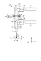
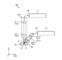
- FIG. 1 is an exemplary schematic configuration diagram of the laser welding apparatus of the first embodiment.
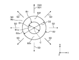
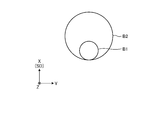
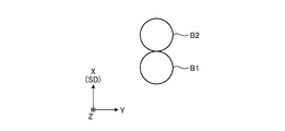
- FIG. 2 is an exemplary schematic view showing a beam (spot) of laser light formed on the surface of a processing target by the laser welding apparatus of the first embodiment.
- FIG. 3 is a graph showing the light absorption rate of each metal material with respect to the wavelength of the laser light to be irradiated.
- FIG. 4 is an exemplary and schematic cross-sectional view of the welded portion of the embodiment.
- FIG. 5 is an exemplary and schematic cross-sectional view showing a part of the welded portion of the embodiment.
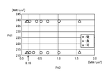
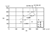
- FIG. 6 is a graph showing the results of welding experiments in the combination of the power density of the first laser beam and the power density of the second laser beam by the laser welding apparatus of the first embodiment.
- FIG. 1 is an exemplary schematic configuration diagram of the laser welding apparatus of the first embodiment.
- FIG. 2 is an exemplary schematic view showing a beam (spot) of laser light formed on the surface of a processing target by the laser welding
- FIG. 7 is a graph showing the results of welding experiments in the combination of the width of the welded portion and the diameter of the second spot when the first laser beam of the laser welding apparatus of the first embodiment is irradiated alone.
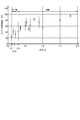
- FIG. 8 is a graph showing the correlation between the output ratio, which is the ratio of the power of the first laser beam to the power of the second laser beam by the laser welding apparatus of the embodiment, and the spatter suppression rate.
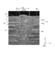
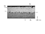
- FIG. 9 is an exemplary and schematic cross-sectional view of the welded portion of the embodiment, which is a cross-sectional view taken along the sweep direction and orthogonal to the surface.
- FIG. 10 is an exemplary and schematic cross-sectional view of a welded portion formed by a single irradiation of the first laser beam with the same power as in FIG.
- FIG. 9 as a reference example, and is a cross-sectional view taken along the sweep direction and with the surface. It is sectional drawing in the orthogonal cross section.
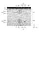
- FIG. 11 is an enlarged view of a part of FIG. 9.
- FIG. 12 is an explanatory view showing a case where the first reference line is applied to one position in the cross section of the welded portion of the embodiment.
- FIG. 13 is an explanatory view showing a case where a second reference line is applied to one position in the cross section of the welded portion of the embodiment.
- FIG. 14 is an exemplary schematic configuration diagram of the laser welding apparatus of the second embodiment.
- FIG. 15 is an explanatory diagram showing the concept of the principle of the diffractive optical element included in the laser welding apparatus of the second embodiment.
- FIG. 16 is an exemplary schematic configuration diagram of the laser welding apparatus of the third embodiment.
- FIG. 17 is an exemplary schematic configuration diagram of the laser welding apparatus of the fourth embodiment.
- FIG. 18 is an exemplary schematic configuration diagram of the laser welding system of the fifth embodiment.
- FIG. 19 is an exemplary schematic configuration diagram of the laser welding system of the sixth embodiment.
- FIG. 20 is an exemplary schematic configuration diagram of the laser welding apparatus of the seventh embodiment.
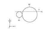
- FIG. 21 is a schematic view showing an example of a beam (spot) of laser light formed on the surface of a processing target by the laser welding apparatus of the seventh embodiment.
- FIG. 22 is a schematic view showing an example of a beam (spot) of laser light formed on the surface of the object to be processed by the laser welding apparatus of the seventh embodiment.
- FIG. 23 is a schematic view showing an example of a beam (spot) of laser light formed on the surface of the object to be processed by the laser welding apparatus of the seventh embodiment.
- FIG. 24 is an exemplary schematic configuration diagram of the laser welding apparatus of the eighth embodiment.
- FIG. 25 is an exemplary schematic configuration diagram of the laser welding apparatus of the ninth embodiment.
- FIG. 26 is a schematic view showing an example of a beam (spot) of laser light formed on the surface of a processing target by the laser welding apparatus of the embodiment.
- FIG. 27 is an exemplary and schematic cross-sectional view of a cross section along the sweep direction of the welded portion of the embodiment and orthogonal to the surface, and is a cross-sectional view of the front end portion of the welded portion in the sweep direction.
- FIG. 24 is an exemplary schematic configuration diagram of the laser welding apparatus of the eighth embodiment.
- FIG. 25 is an exemplary schematic configuration diagram of the laser welding apparatus of the ninth embodiment.
- FIG. 26 is a schematic view showing an example of a beam
- FIG. 28 is an exemplary and schematic cross-sectional view in a cross section along the sweep direction of the weld formed by a single irradiation of the first laser beam with the same power as in the case of FIG. 27 and orthogonal to the surface. It is a cross-sectional view of the front end portion of the welded portion in the sweep direction.
- the X direction is represented by an arrow X
- the Y direction is represented by an arrow Y
- the Z direction is represented by an arrow Z.
- the X, Y, and Z directions intersect and are orthogonal to each other.
- the Z direction is the normal direction of the surface Wa (processed surface) of the processing target W.
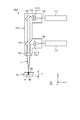
- FIG. 1 is a schematic configuration diagram of the laser welding apparatus 100 of the first embodiment.
- the laser welding device 100 includes a laser device 111, a laser device 112, an optical head 120, and an optical fiber 130.
- Each of the laser devices 111 and 112 has a laser oscillator, and as an example, it is configured to be able to output a laser beam having a power of several kW. Further, the laser devices 111 and 112 may be configured to include, for example, a plurality of semiconductor laser elements inside and to output a multimode laser beam having a power of several kW as the total output of the plurality of semiconductor laser elements. good. Further, the laser devices 111 and 112 may be provided with various laser light sources such as a fiber laser, a YAG laser, and a disk laser.
- the laser device 111 outputs the first laser beam having a wavelength of 800 [nm] or more and 1200 [nm] or less.
- the laser device 111 is an example of the first laser device.
- the laser oscillator included in the laser device 111 is an example of the first laser oscillator.
- the laser device 112 outputs a second laser beam having a wavelength of 500 [nm] or less.
- the laser device 112 is an example of a second laser device.
- the laser device 112 preferably outputs a second laser beam having a wavelength of 400 [nm] or more and 500 [nm] or less.
- the laser oscillator included in the laser device 112 is an example of a second laser oscillator.
- the optical fiber 130 guides the laser light output from the laser devices 111 and 112 to the optical head 120, respectively.
- the optical head 120 is an optical device for irradiating the laser beam input from the laser devices 111 and 112 toward the processing target W.
- the optical head 120 includes a collimating lens 121, a condenser lens 122, a mirror 123, and a filter 124.
- the collimating lens 121, the condenser lens 122, the mirror 123, and the filter 124 may also be referred to as optical components.
- the optical head 120 is configured so that the relative position with the processing target W can be changed in order to sweep the laser light L while irradiating the surface Wa of the processing target W with the laser light L.
- the relative movement of the optical head 120 and the processing target W can be realized by the movement of the optical head 120, the movement of the processing target W, or the movement of both the optical head 120 and the processing target W.
- the optical head 120 may be configured to be able to sweep the laser beam L on the surface Wa by having a galvano scanner or the like (not shown).
- the collimating lens 121 (121-1, 121-2) collimates the laser beam input via the optical fiber 130, respectively.
- the collimated laser beam becomes parallel light.
- the mirror 123 reflects the first laser beam that has become parallel light by the collimating lens 121-1.
- the first laser beam reflected by the mirror 123 travels in the opposite direction to the Z direction and heads toward the filter 124.
- the mirror 123 is not required in the configuration in which the first laser beam is input to the optical head 120 so as to travel in the direction opposite to the Z direction.
- the filter 124 is a high-pass filter that transmits the first laser beam and reflects the second laser beam without transmitting it.
- the first laser beam passes through the filter 124, travels in the opposite direction in the Z direction, and travels toward the condenser lens 122.
- the filter 124 reflects the second laser beam that has become parallel light by the collimating lens 121-2.
- the second laser beam reflected by the filter 124 travels in the opposite direction to the Z direction and heads toward the condenser lens 122.
- the condensing lens 122 condenses the first laser light and the second laser light as parallel light, and irradiates the processing target W as the laser light L (output light).
- the processing target W is an example of a metal member.
- a welded portion 14 is formed on the processing target W.
- the welded portion 14 extends from the front surface Wa toward the back surface Wb and linearly extends along the front surface Wa in the sweep direction SD.
- the front surface Wa is an example of the first surface
- the back surface Wb is an example of the second surface.
- FIG. 2 is a schematic view showing a beam (spot) of the laser beam L irradiated on the surface Wa of the processing target W.
- the beam of the laser beam L is such that the beam B1 of the first laser beam and the beam B2 of the second laser beam overlap each other, and the beam B2 is larger (wider) than the beam B1.
- the outer edge B2a of the beam B2 is formed so as to surround the outer edge B1a of the beam B1.
- the beam B1 is an example of the first spot
- the beam B2 is an example of the second spot.
- the arrow SD shown in FIG. 2 indicates the sweep direction.
- the shape of the beam (spot) of the laser beam L is the same for any sweep direction SD. .. Therefore, when a moving mechanism for relatively moving the optical head 120 and the processing target W for sweeping the surface Wa of the laser beam L is provided, the moving mechanism should have at least a relatively translatable mechanism. However, the relatively rotatable mechanism may be omitted.
- Each W to be processed can be made of a metal material having a relatively high thermal conductivity.
- the metal material is, for example, a copper-based metal material, an aluminum-based metal material, a nickel-based metal material, an iron-based metal material, a titanium-based metal material, or the like, and specifically, copper, a copper alloy, an aluminum, or an aluminum alloy. , Tin, nickel, nickel alloy, iron, stainless steel, titanium, titanium alloy, etc.
- the processing target W is an example of a metal member.
- FIG. 3 is a graph showing the light absorption rate of each metal material with respect to the wavelength of the laser beam L to be irradiated.
- the horizontal axis of the graph of FIG. 3 is the wavelength, and the vertical axis is the absorption rate.
- FIG. 3 shows the relationship between wavelength and absorption rate for aluminum (Al), copper (Cu), gold (Au), nickel (Ni), silver (Ag), tantalum (Ta), and titanium (Ti). It is shown.
- a blue or green laser beam (second laser) is used rather than using a general infrared (IR) laser beam (first laser beam). It can be understood that the energy absorption rate is higher when light) is used. This feature becomes remarkable in copper (Cu), gold (Au), and the like.
- the laser beam When the laser beam is applied to the processing target W, which has a relatively low absorption rate with respect to the wavelength used, most of the light energy is reflected and does not affect the processing target W as heat. Therefore, it is necessary to apply a relatively high power to obtain a melting region having a sufficient depth. In that case, energy is suddenly applied to the central part of the beam, so that sublimation occurs and a keyhole is formed.
- the wavelength of the first laser light, the wavelength of the second laser light, and the wavelength of the processing target W are such that the absorption rate of the processing target W with respect to the second laser light is higher than the absorption rate of the processing target W with respect to the first laser light.
- the material is selected.
- the portion to be welded (hereinafter referred to as the welded portion) of the processing target W by sweeping the spot of the laser beam L is first, second.
- the second laser beam is irradiated by the region B2f of the beam B2 of the laser beam located in front of the SD in FIG.
- the welded portion is irradiated with the beam B1 of the first laser beam, and then the second laser beam is irradiated again by the region B2b of the beam B2 of the second laser beam located behind the sweep direction SD1.
- a heat conduction type melting region is first generated by irradiation with a second laser beam having a high absorption rate in the region B2f. After that, a deeper keyhole-type molten region is generated in the welded portion by irradiation with the first laser beam.
- the required depth is obtained by the first laser beam having a lower power than in the case where the heat conduction type melting region is not formed.
- a molten region can be formed.
- the welded portion is changed in a molten state by irradiation with a second laser beam having a high absorption rate in the region B2b.
- the wavelength of the second laser beam is preferably 550 nm or less, and more preferably 500 nm or less.
- the processing target W is set so that the laser beam L irradiates the surface Wa of the processing target W. Then, in a state where the surface Wa is irradiated with the laser beam L including the beam B1 and the beam B2, the laser beam L and the processing target W are relatively moved. As a result, the laser beam L moves (sweeps) in the sweep direction SD on the surface Wa while being irradiated on the surface Wa. The portion irradiated with the laser beam L is melted and then solidified as the temperature decreases, so that the processing target W is welded.
- FIG. 4 is a cross-sectional view of the welded portion 14 formed on the processing target W.
- FIG. 4 is a cross-sectional view perpendicular to the sweep direction SD (X direction) and along the thickness direction (Z direction).
- the welded portion 14 extends in the sweep direction SD, that is, in the direction perpendicular to the paper surface of FIG.
- FIG. 4 shows a cross section of the welded portion 14 formed on the processing target W, which is a single copper plate having a thickness of 2 [mm].
- the form of the welded portion 14 formed of a plurality of plate-shaped metal materials stacked in the thickness direction (Z direction) is substantially the same as the form of the welded portion formed of one metal material having the same thickness. Can be presumed to be.
- the welded portion 14 has a weld metal 14a extending from the surface Wa in the opposite direction in the Z direction, and a heat-affected zone 14b located around the weld metal 14a. ..
- the weld metal 14a is a portion that is melted by irradiation with the laser beam L and then solidified.
- the weld metal 14a can also be referred to as a melt-solidified portion.
- the heat-affected zone 14b is a portion where the base material of the processing target W is thermally affected and is not melted.
- the width of the weld metal 14a along the Y direction becomes narrower as the distance from the surface Wa increases. That is, the cross section of the weld metal 14a has a tapered shape that narrows in the direction opposite to the Z direction.
- the weld metal 14a includes a first portion 14a1 separated from the surface Wa and a second portion 14a2 between the first portion 14a1 and the surface Wa. There was found.
- the first portion 14a1 is a portion obtained by melting the keyhole type by irradiation with the first laser beam
- the second portion 14a2 is a region located behind the sweep direction SD1 in the beam B2 of the second laser beam. It is a part obtained by melting by irradiation of B2b.
- the crystal grain size is different between the first site 14a1 and the second site 14a2, specifically, the X direction (sweep direction). It was found that the average cross-sectional area of the crystal grains at the second site 14a2 was larger than the average cross-sectional area of the crystal grains at the first site 14a1 in the cross section orthogonal to SD).
- the inventors have found that when the welded portion is irradiated with only the beam B1 of the first laser beam, that is, when the region B2b located behind the sweep direction SD1 in the beam B2 is not irradiated, the second It was confirmed that the site 14a2 was not formed and the first site 14a1 extended deeply from the surface Wa in the opposite direction to the Z direction. That is, in the present embodiment, the second portion 14a2 is formed near the surface Wa by the irradiation of the region B2b located behind the sweep direction SD1 in the beam B2, so that the first portion 14a1 is the said. It can be presumed that the second portion 14a2 is formed at a position opposite to the surface Wa, in other words, at a position separated from the surface Wa in the opposite direction in the Z direction.
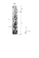
- FIG. 5 is a cross-sectional view showing a part of the welded portion 14.
- FIG. 5 shows the boundaries of the crystal grains obtained by the EBSD method.
- crystal grains A having a crystal grain size of 13 [ ⁇ m] or less are painted black. Note that 13 [ ⁇ m] is not a threshold value of physical characteristics, but a threshold value set for analysis of the experimental results.
- the crystal grains A are relatively abundant in the first portion 14a1 and relatively abundant in the second portion 14a2. That is, the average cross-sectional area of the crystal grains in the second site 14a2 is larger than the average cross-sectional area of the crystal grains in the first site 14a1.
- the inventors have found that the average cross-sectional area of the crystal grains in the second site 14a2 is 1.8 times or more the average cross-sectional area of the crystal grains in the first site 14a1. It was confirmed.
- such relatively small crystal grains A are densely packed in a state of being elongated in the Z direction at a position separated from the surface Wa in the Z direction. There is. Further, from the analysis at a plurality of locations where the positions in the X direction (sweep direction SD) are different, it is confirmed that the region where the crystal grains A are densely extends also extends to the sweep direction SD. Since the welding is performed while sweeping, it can be estimated that crystals are formed in the same shape in the sweep direction SD.
- first region Z1 and second region Z2 may be designated as the first region 14a1 and the second region 14a2, respectively.
- the first region Z1 and the second region Z2 are square regions extending in the Z direction with a width wm (equal width in the Y direction) in a cross section orthogonal to the sweep direction SD, and the second region Z2.
- the first region Z1 is a region deeper than the depth d, in other words, a region opposite to the surface Wa with respect to the position of the depth d. can do.
- the width wm is, for example, 1/3 of the width wb (average value of the bead width) on the surface Wa of the weld metal 14a, and the depth d (height, thickness) of the second region Z2 is, for example, the width wb. Can be 1/2 of.
- the depth of the first region Z1 can be, for example, three times the depth d of the second region Z2.
- the inventors According to an experimental analysis of a plurality of samples, the inventors have found that in such a setting of the first region Z1 and the second region Z2, the average value of the cross-sectional areas of the crystal grains in the second region Z2 is in the first region Z1. It was confirmed that it was larger than the average value of the cross-sectional area of the crystal grains and was 1.8 times or more. Such a relationship between the size of the crystal grains in the first region Z1 and the second region Z2 is considered to be a factor for realizing a strong welding strength in the processing target W, and such discrimination is also made by welding the weld metal. It can be evidence that the first site 14a1 and the second site 14a2 are formed at 14a.
- the thickness T (see FIG. 1) of the processing target W by laser welding of the present embodiment is 0.05 [mm] or more and 2.0 [mm] or less. It was found that similar results can be obtained in the case of.
- FIG. 6 is a graph showing the experimental results of welding in the combination of the power density Pd1 of the first laser beam and the power density Pd2 of the second laser beam on the surface Wa of the processing target W.
- “ ⁇ ” indicates that the number of spatters and blow holes is very small (excellent)
- “ ⁇ ” indicates that the number of spatters and blow holes is small (good)
- ⁇ indicates that the number of spatters and blow holes is small.
- some other inconvenience occurs (possible) such as a large energy loss is shown.
- “excellent” indicates the case where the number of blow holes per unit length (for example, 1 [cm]) of the linear welded portion is 1 or less, and “good” and “possible”. ”Indicates a case where the number of blow holes per unit length of the welded portion is 2 or more and less than 5. Further, in this experiment, the wavelength of the first laser beam is 1070 [nm] and the output is 1.5 [kW], the wavelength of the second laser beam is 450 [nm], and the output is 150 [W]. ]Met.
- Each of the beam B1 and the beam B2 has, for example, a Gaussian-shaped power distribution in the radial direction of the cross section orthogonal to the optical axis direction of the beam.
- the power distribution of the beams B1 and B2 is not limited to the Gaussian shape.
- the diameter of the circle representing the beams B1 and B2 is the beam diameter of each beam B1 and B2.
- Beam diameter of each beam B1, B2 includes a peak of the beam is defined as the diameter of the region of 1 / e 2 or more of the intensity of the peak intensity.
- the length of a region having an intensity of 1 / e 2 or more of the peak intensity in the direction perpendicular to the sweep direction SD can be defined as the beam diameter.
- the beam diameter on the surface Wa of the processing target W is referred to as a spot diameter.
- FIG. 7 is a diagram showing the experimental results of welding by combining the width wb (bead width) of the welded portion when the beam B1 is irradiated alone and the spot diameter D2 (outer diameter, see FIG. 2) of the beam B2.
- the meanings and criteria of the symbols ( ⁇ , ⁇ , ⁇ ) in FIG. 7 are the same as those in FIG. Further, in this experiment, the wavelength of the first laser beam is 1070 [nm] and the output is 1 [kW], the wavelength of the second laser beam is 450 [nm] and the output is 400 [W]. there were.
- the spatter suppression rate Rs is defined as the following equation (2).
- Rs 1-Nh / Nir ⁇ ⁇ ⁇ (2)
- Nh is the number of spatters generated in a predetermined area when both the first laser beam and the second laser beam are irradiated
- Nir is only the first laser beam with the same power as when measuring Nh.
- FIG. 8 shows the results of conducting experiments a plurality of times at each output ratio.
- the line segment corresponding to the output ratio indicates the range of variation in the spatter suppression rate in the experimental results of multiple samples (at least 3 samples or more) at the output ratio, and ⁇ indicates the median value of the spatter suppression rate for each output ratio.
- the output ratio Rp is preferably 0.1 or more and less than 0.18 ( ⁇ ), and 0.18 or more and less than 0.3. It was found that the above case is more preferable ( ⁇ ), and the case of 0.3 or more and 2 or less is more preferable ( ⁇ ⁇ ).
- the inventors conducted experiments on a plurality of samples at different sweep velocities, and found that the occurrence of spatter and blow holes differs depending on the sweep velocities.
- the sweep rate is preferably 50 [mm / s] or more, and more preferably 100 [mm / s] or more. found.
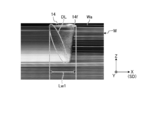
- FIG. 9 is a cross-sectional view of the welded portion 14 formed by irradiation of both the first laser beam and the second laser beam in a cross section along the sweep direction and orthogonal to the surface Wa.
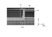
- FIG. 10 is a cross-sectional view of the welded portion 14 formed by a single irradiation of the first laser beam with the same power as in FIG. 9 as a reference example in a cross section along the sweep direction and orthogonal to the surface Wa. be.
- the conditions other than the single irradiation of the first laser beam in the example of FIG. 10 are set in the same manner as in the case of the example of FIG.
- FIG. 11 is an enlarged view of a part of FIG. 9.
- the depth from the surface Wa It was found that the orientations (longitudinal direction, growth direction) of the crystal grains differed according to the above. This is obtained by melting the third portion 14a3 obtained by the keyhole-type melting by the irradiation of the first laser beam and the region B2b located behind the sweep direction in the beam B2 of the second laser beam.
- the third portion 14a3 is a portion located away from the surface Wa and corresponds to the above-mentioned first portion 14a1.
- the fourth part 14a4 is a part located between the third part 14a3 and the surface Wa, and is a part corresponding to the above-mentioned second part 14a2.
- JIS G 0551: 2020 A.M. 2 Based on the cutting method, an index showing the direction (longitudinal direction) of the crystal grains in each part in the welded part 14 was defined.
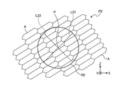
- first reference line R1 and second reference line R2 including two linear test lines orthogonal to each other are used in the cross-sectional image.
- first reference line R1 is shown by a solid line
- second reference line R2 is shown by a broken line.
- the first reference line R1 has two diameters orthogonal to each other of the reference circle R0 as the straight line test lines L11 and L12, and one straight line test line L11 is in the X direction (sweep direction) along the surface Wa.
- the other linear test line L12 extends in the Z direction orthogonal to the surface Wa.
- the second reference line R2 has two diameters orthogonal to each other of the same reference circle R0 as the first reference line R1 as the straight line test lines L21 and L22, and one straight line test line L21 is X.
- the other linear test line L12 Extending in the direction between the direction and the Z direction, the other linear test line L12 is in the direction between the opposite direction of the X direction and the Z direction, or the direction between the opposite direction of the Z direction and the X direction. , Is extending.
- the angle difference between the linear test line L11 and the linear test line L21 is 45 ° or 135 °
- the angular difference between the linear test line L12 and the linear test line L22 is 45 ° or 135 °.
- the length of the diameter of the reference circle R0 that is, the length of the linear test lines L11, L12, L21, and L22 is, for example, a length corresponding to 200 [ ⁇ m] (a predetermined length). However, it can be appropriately set according to the size of the crystal grains.
- the number of crystal grains can also be referred to as the number of grain boundaries. Further, in the formula (3-2), when (N22 / N21) is (N21 / N22) or more, max (N22 / N21, N21 / N22) is (N22 / N21), and (N22 / N21). When is less than (N21 / N22), max (N22 / N21, N21 / N22) is (N21 / N22). In the actual measurement, in the micrograph of the XZ cross section taken at 50 times, the above measurement can be performed at an arbitrary predetermined location or more, for example, 10 or more locations, and the average values thereof can be Rb1 and Rb2, respectively. .. When any one of N11, N12, N21, and N22 becomes 0 at a certain point P in the welded portion 14, the number of grain boundaries at the point P does not have to be used for the calculation of Rb1 and Rb2.
- FIGS. 12 and 13 are schematics showing a case where the first reference line R1 is applied (FIG. 12) and a case where the second reference line R2 is applied to one point P in the cross section of the welded portion 14 (FIG. 13).
- the number of crystal grains A (grain boundaries) intersecting the linear test lines L11, L12, L21, and L22 is different.
- the grain boundary number N21 is smaller than the other grain boundary numbers N11, N12, and N22. Therefore, the point P shown in the examples of FIGS.
- the second grain boundary number ratio Rb2 is higher than the first grain boundary number ratio Rb1.
- the first grain boundary number ratio Rb1 is relatively high and the second grain boundary is second. It becomes larger than the grain boundary number ratio Rb2.
- the second grain boundary number ratio Rb2 is relatively high and the second grain boundary ratio Rb2 is relatively high. It becomes larger than the grain boundary number ratio Rb1.
- the first grain boundary number ratio Rb1 at each point P in the fourth site 14a4 is lower than the first grain boundary number ratio Rb1 at each point P in the third site 14a3.
- the second grain boundary number ratio Rb2 at each point P in the fourth site 14a4 is higher than the second grain boundary number ratio Rb2 at each point P in the third site 14a3.
- the first grain boundary number ratio Rb1 is higher than the second grain boundary number ratio Rb2, and at each point P in the fourth site 14a4, the second grain boundary number. It was found that the ratio Rb2 was higher than the first grain boundary number ratio Rb1.
- first grain boundary ratio Rb1 and the second grain boundary ratio Rb2 in the welded portion 14 is considered to be a factor for realizing a strong welding strength in the work target W.
- the arithmetic average roughness Ra of the surface Wa of the processing target W is determined. It was found that good results (corresponding to the above “excellent") can be obtained even when the value is 21 [ ⁇ m] or less.
- the experiment was carried out in each case where the arithmetic mean roughness Ra was 21 [ ⁇ m], 8 [ ⁇ m], and 6 [ ⁇ m], and good results were obtained in each case.
- the conventional laser welding apparatus when the surface Wa is close to a mirror surface, for example, the laser beam is reflected by the surface Wa, which may make welding difficult or impossible.
- the arithmetic average roughness Ra is 21 [ ⁇ m] or less, and even lower 8 [ ⁇ m] or 6 [ ⁇ m]. Even for a processing target W having a surface Wa close to a mirror surface, better welding can be performed by a laser beam having a lower power.
- the processing target W is welded, for example, by irradiating the surface Wa with a laser beam L so that the spot moves relatively along the surface Wa. ..
- the laser light L includes a first laser light having a wavelength of 800 [nm] or more and 1200 [nm] or less, and a second laser light having a wavelength of 550 [nm] or less.
- the wavelength of the second laser beam is preferably 400 [nm] or more and 500 [nm] or less.
- the beam B2 (second irradiation region) of the second laser light is wider than the beam B1 (first irradiation region) of the first laser light, and the outer edge of the beam B2.
- B2a (second outer edge) surrounds the outer edge B1a (first outer edge) of the beam B1.
- the processing target W is made of any one of a copper-based metal material, an aluminum-based metal material, a nickel-based metal material, an iron-based metal material, and a titanium-based metal material.
- the metal material may or may not have conductivity.
- the effect of the welding method of this embodiment can be obtained when the processing target W is made of any of the above materials.
- At least a part of the beam B2 (second spot) of the second laser beam is in the sweep direction SD more than the beam B1 (first spot) of the first laser beam. It is located in front.
- the beam B1 and the beam B2 overlap at least partially on the surface Wa.
- the beam B2 is wider than the beam B1.
- the outer edge B2a (second outer edge) of the beam B2 surrounds the outer edge B1a (first outer edge) of the beam B1.
- the width wb of the welded portion and the spot diameter D2 when the beam B1 is irradiated as a single substance are described in the following equation (1). wb-400 ⁇ D2 ⁇ wb + 400 ... (1)
- the spot diameter D2 is set so as to satisfy the above conditions.
- the output ratio of the power of the second laser light to the power of the first laser light is 0.1 or more and 2 or less.
- the inventors have confirmed that welding defects can be reduced in welding by irradiation with a beam of laser light L that forms such beams B1 and B2 on the surface Wa.
- the processing target W is preheated by the region B2f of the beam B2 before the beam B1 arrives, so that the molten pool of the processing target W formed by the beam B2 and the beam B1 is formed. It can be presumed that this is for stabilization. Therefore, according to the laser beam L having such beams B1 and B2, for example, welding with less welding defects and higher welding quality can be performed. Further, according to such settings of the beams B1 and B2, for example, there is an advantage that the power of the first laser beam can be further lowered. Further, when the beam B1 and the beam B2 are irradiated coaxially, there is an advantage that the relative rotation between the optical head 120 and the processing target W becomes unnecessary.
- the weld metal 14a of the processing target W (metal member) of the present embodiment is the first portion 14a1 located apart from the surface Wa (first surface) in the thickness direction (opposite direction in the Z direction). It has a second site 14a2, which is located between the first site 14a1 and the surface Wa and has a larger average cross-sectional area of crystal grains than the first site 14a1.
- the average value of the cross-sectional areas of the crystal grains contained in the second portion 14a2 is included in the first portion 14a1. It is 1.8 times or more the average value of the cross-sectional area of the crystal grains.
- such a welded portion 14 sweeps a beam of laser light L having a beam B1 of the first laser light and a beam B2 of the second laser light onto the surface Wa as shown in FIG. It was obtained by irradiating the SD while sweeping. Further, as described above, the inventors have experimentally confirmed that welding defects can be reduced in welding by irradiation with a beam of laser light L as shown in FIG. Therefore, according to the above configuration, for example, it is possible to obtain a work target W (metal member) having a welded portion 14 having less welding defects and higher welding quality. Further, according to the present embodiment, for example, the power of the first laser beam can be made lower, and the relative rotation between the optical head 120 and the processing target W becomes unnecessary. ..
- the metal member as the processing target W can be applied to various electric parts and electronic devices having the electric parts.
- Electrical components are conductors, such as terminals, busbars, coils, and battery tabs.
- the electronic device has, for example, the conductor, and specifically, a motor, an assembled battery, an inverter, a computer, and the like.
- FIG. 14 is a schematic configuration diagram of the laser welding apparatus 100A of the second embodiment.
- the optical head 120 has a DOE 125 between the collimating lens 121-1 and the mirror 123. Except for this point, the laser welding apparatus 100A has the same configuration as the laser welding apparatus 100 of the first embodiment.
- DOE125 forms the shape of the beam B1 of the first laser beam (hereinafter referred to as the beam shape).
- the DOE 125 has, for example, a configuration in which a plurality of diffraction gratings 125a having different periods are superposed.
- the DOE 125 can form a beam shape by bending or superimposing parallel light in a direction affected by each diffraction grating 125a.
- DOE125 can also be referred to as a beam shaper.
- the optical head 120 is provided after the collimating lens 121-2 to adjust the beam shape of the second laser beam, and is provided after the filter 124 to adjust the beam shapes of the first laser beam and the second laser beam. It may have a beam shaper or the like to be adjusted. By appropriately adjusting the beam shape of the laser beam L with the beam shaper, the occurrence of welding defects in welding can be further suppressed.
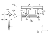
- FIG. 16 is a schematic configuration diagram of the laser welding apparatus 100B of the third embodiment.
- the optical head 120 has a galvano scanner 126 between the filter 124 and the condenser lens 122. Except for this point, the laser welding apparatus 100B has the same configuration as the laser welding apparatus 100 of the first embodiment.
- the galvano scanner 126 has two mirrors 126a and 126b, and by controlling the angles of the two mirrors 126a and 126b, the irradiation position of the laser beam L can be set without moving the optical head 120. It is a device that can be moved to sweep the laser beam L. The angles of the mirrors 126a and 126b are changed by, for example, a motor (not shown). According to such a configuration, a mechanism for relatively moving the optical head 120 and the processing target W becomes unnecessary, and for example, an advantage that the device configuration can be miniaturized can be obtained.
- FIG. 17 is a schematic configuration diagram of the laser welding apparatus 100C of the fourth embodiment.
- the optical head 120 has a DOE 125 (beam shaper) between the collimating lens 121-2 and the filter 124.
- the laser welding apparatus 100C has the same configuration as the laser welding apparatus 100B of the third embodiment. According to such a configuration, the same effect as the third embodiment by having the galvano scanner 126 and the same effect as the second embodiment by having the DOE 125 (beam shaper) can be obtained.
- the optical head 120 is provided after the collimating lens 121-1 and is provided after the beam shaper for adjusting the beam shape of the first laser beam, and is provided after the filter 124 and is provided with the first laser beam and the second laser beam. It may have a beam shaper or the like that adjusts the beam shape of the laser beam.
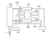
- FIG. 18 is a schematic configuration diagram of a laser welding system 1000 including the laser welding apparatus 100 of the first embodiment.
- the laser welding system 1000 may be provided with the laser welding devices 100A to 100C of other embodiments instead of the laser welding device 100.
- the laser welding system 1000 includes a main power supply 1001, a sub power supply 1002, 1003, an integrated controller 1004, and a cooling mechanism 1005 in addition to the laser welding device 100.
- the main power supply 1001 supplies power to the sub power supplies 1002 and 1003. Further, the sub power source 1002 supplies electric power to the laser device 111, and the sub power source 1003 supplies electric power to the laser device 112.
- the integrated controller 1004 controls the operation of both the laser device 111 and the laser device 112. Specifically, it is possible to control the power of the laser light output from the laser devices 111 and 112, the timing of oscillation, and the wavelength, and also control the operation related to sweeping, for example, the operation of the relative movement mechanism and the galvano scanner 126. can. As a result, the laser device 111 (first laser oscillator) and the laser device 112 (second laser oscillator) can be controlled more reliably and comprehensively.
- the integrated controller 1004 is an example of a control unit.
- the cooling mechanism 1005 includes a pipe 1006 through which a refrigerant such as a coolant flows.
- the pipe 1006 is arranged so as to pass through the laser devices 111 and 112 and the optical head 120, respectively.
- the cooling mechanism 1005 can switch between supplying and stopping the refrigerant flowing through each pipe 1006, change the flow rate, and adjust the temperature of the refrigerant.
- the laser devices 111 and 112 and the optical head 120 can be cooled, for example, the operation of the laser devices 111 and 112 can be stabilized, and the excessive temperature rise of the optical head 120 can be suppressed.
- the operation of the cooling mechanism 1005 may be controlled by the integrated controller 1004.
- FIG. 19 is a schematic configuration diagram of a laser welding system 1000A including the laser welding apparatus 100 of the first embodiment.
- the laser welding system 1000A may include the laser welding devices 100A to 100C of other embodiments instead of the laser welding device 100.
- the fifth embodiment except that the laser welding system 1000A includes a controller 1004-1 for the laser device 111 and a controller 1004-2 for the laser device 112 instead of the integrated controller 1004. It has the same configuration as the laser welding system 1000 of the form. Even with such a configuration, the same effect as that of the laser welding system 1000 of the fifth embodiment can be obtained.
- the controllers 1004-1 and 1004-2 are examples of control units.
- FIG. 20 is a schematic configuration diagram of the laser welding apparatus 100D of the seventh embodiment.
- the laser welding apparatus 100D is modified based on the laser welding apparatus 100 of the first embodiment.
- the optical head 120 has a first portion 120-1, a second portion 120-2, and a third portion 120-3.
- the first site 120-1 includes a collimating lens 121-1 and a mirror 123.
- the second site 120-2 includes a collimating lens 121-2, a filter 124, and a condenser lens 122.
- the third site 120-3 is interposed between the first site 120-1 and the second site 120-2.
- the first portion 120-1 and the third portion 120-3 are configured to be relatively slidable in the X direction or the opposite direction of the X direction without changing the posture with respect to the Z direction.
- the second portion 120-2 and the third portion 120-3 are configured to be relatively slidable in the opposite directions of the Y direction and the Y direction without changing the posture with respect to the Z direction.
- the outlet of the first laser beam of the first portion 120-1 and the inlet of the first laser beam of the second portion 120-2 are directed in directions orthogonal to the optical axis direction of the first laser beam, respectively.
- An annular and plate-shaped flange 120a that expands is provided.
- a third portion 120-3 having an annular shape and a plate shape spreading in a direction orthogonal to the optical axis direction of the first laser beam is sandwiched between these two flanges 120a.
- the two flanges 120a and the third portion 120-3 can slide relatively along their respective contact surfaces with no change in attitude with respect to the Z axis.
- a guide mechanism (not shown) that guides the relative slide in the X direction and can be fixed at an arbitrary relative position in the X direction is provided between the first portion 120-1 and the third portion 120-3.
- a guide mechanism (not shown) that guides the relative slide in the Y direction and can be fixed at an arbitrary relative position in the Y direction is provided between the second portion 120-2 and the third portion 120-3.
- the optical axis of the first laser beam input to the filter 124 and output from the filter 124 and the optical axis of the second laser beam output from the filter 124 Can be shifted in a direction orthogonal to those optical axes. Since the first portion 120-1 and the laser device 111 and the second portion 120-2 and the laser device 112 are connected by an optical fiber 130 having flexibility, the first portion 120-1 and the laser apparatus 112 are connected to each other. The laser devices 111 and 112 can be fixed even when the position of the one site 120-1 or the second site 120-2 changes.
- FIGS. 21 to 23 show examples of laser beam B1 and B2 formed on the surface Wa of the processing target W by the laser welding apparatus 100D.
- the relative positions of the beams B1 and B2 can be arbitrarily changed.
- at least a part of the beam B2 (second spot) is located in front of the beam B1 (first spot) in the sweep direction SD on the surface Wa as shown in FIGS. 21 to 23. It has been found that the same effect as in the first embodiment can be obtained by the preheating effect of the beam B2 when the beam B1 and the beam B2 are in contact with each other or at least partially overlap each other.
- FIGS. 21 to 23 are merely examples, and the arrangement of the beams B1 and B2 obtained by the laser welding apparatus 100D and the sizes of the beams B1 and B2 are not limited to the examples of FIGS. 21 to 23.
- the fact that the beam B2 is located in front of the sweep direction SD with respect to the beam B1 is a virtual straight line on the surface Wa that passes through the front end of the sweep direction SD of the beam B1 and is orthogonal to the sweep direction SD. It means that at least a part of the beam B2 is present in the region in front of the SD in the sweep direction with respect to the VL.
- FIG. 24 is a schematic configuration diagram of the laser welding apparatus 100E of the eighth embodiment.
- the laser welding apparatus 100E is modified based on the laser welding apparatus 100B of the third embodiment.
- the laser welding device 100B has a position adjusting mechanism 140 that variably sets the position of the collimating lens 121 in the optical axis direction.
- the position adjusting mechanism 140 can appropriately change the sizes (spot diameters D1 and D2) of the beams B1 and B2 on the surface Wa of the processing target W. That is, the position adjusting mechanism 140 can also be referred to as a spot size variable mechanism.
- the same position adjusting mechanism 140 can be applied to the condenser lens 122, may be applied to both the collimating lens 121 and the condenser lens 122, or the laser welding apparatus of another embodiment. It can also be applied to a collimating lens 121 and a condenser lens 122 of 100, 100A, 100C, 100D, and 100F.
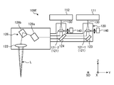
- FIG. 25 is a schematic configuration diagram of the laser welding apparatus 100F of the ninth embodiment.
- the optical head 120 has a first portion 120-1 for irradiating the first laser beam L1 and a second portion 120 for irradiating the second laser beam L2, each of which is composed of different bodies (housings). -2 and are provided. Even with such a configuration, the same actions and effects as those of the above embodiment can be obtained.
- FIG. 26 shows an example of spots of beams B1 and B2 formed on the surface Wa of the processing target W by the laser welding devices 100, 100A to 100F of any of the above-described embodiments.
- the spot diameter of the beam B2 may be substantially the same as the spot diameter of the beam B1. Further, although not shown, the spot diameter of the beam B2 may be smaller than the spot diameter of the beam B1.
- the surface area of the molten pool may be adjusted by sweeping by known wobbling, weaving, output modulation, or the like.
- the processing target may be a metal plate having a thin layer of another metal on the surface of the metal, such as a plated metal plate.
- center of the beam of the first laser beam and the center of the beam of the second laser beam do not necessarily have to coincide with each other, and may be deviated from each other.
- the beam of the first laser beam may be partially located outside the beam of the second laser beam.
- FIG. 27 is a cross-sectional view of the welded portion 14 along the sweep direction SD of the embodiment and in a cross section orthogonal to the surface Wa, and is a cross-sectional view of the front end portion of the welded portion 14 in the sweep direction SD.
- FIG. 28 is a cross-sectional view taken along the sweep direction SD of the welded portion 14 formed by single irradiation of the first laser beam with the same power as in FIG. 27 and in a cross section orthogonal to the surface Wa. It is a cross-sectional view of the front end portion of the welded portion 14 in the sweep direction SD.
- the contour of the molten pool (welded portion 14) is visualized by image processing.
- the molten pool formed in the processing with the hybrid laser that irradiates the first laser beam and the second laser beam of the present embodiment shown in FIG. 27 is a fiber laser that irradiates only the first laser beam shown in FIG. 28.
- the broken line frame DL in FIG. 27 it has a longer tail behind the sweep direction SD as compared with the molten pool formed by the processing in.
- the front portion 14f of the molten pool (welded portion 14) of the present embodiment projects in front of the sweep direction SD.
- the length Lw1 in the sweep direction SD of the molten pool formed in the machining with the hybrid laser is the length Lw2 in the sweep direction SD of the molten pool formed in the machining with the fiber laser (FIG. 27). 28) is longer. That is, in the processing with the hybrid laser, the molten pool is larger than the processing with the fiber laser. According to the hybrid laser processing that irradiates the first laser beam and the second laser beam of the present embodiment, the molten pool expands and the internal thermal convection is more stabilized by the irradiation of the second laser beam (blue laser beam).
- the opening of the keyhole is enlarged and the vapor pressure at the time of evaporation is more easily escaped to the outside. Therefore, the generation of spatter is suppressed and a stable molten pool can be obtained as compared with the single irradiation of the first laser beam. Can be estimated.
- the present invention can be applied to welding methods, laser welding systems, metal members, electrical parts, and electronic devices.
Landscapes
- Physics & Mathematics (AREA)
- Optics & Photonics (AREA)
- Engineering & Computer Science (AREA)
- Plasma & Fusion (AREA)
- Mechanical Engineering (AREA)
- Laser Beam Processing (AREA)
Abstract
Description
wb-400<D2<wb+400 ・・・(1)
を満たすよう、前記第二スポットの外径を設定してもよい。
Rb1=N12/N11 ・・・(3-1)
(ここに、Rb1は、第一粒界数比率、N11は、前記第一表面と直交しかつ前記溶接部の延び方向に沿った試験断面において、前記第一表面に沿った所定の長さの直線試験線と交差した粒界数であり、N12は、前記試験断面において、前記第一表面と直交した方向に延びた前記所定の長さの直線試験線と交差した粒界数である。)と表した場合に、前記溶接金属は、前記第一表面に対して当該第一表面から前記第二表面に向かう厚さ方向に離れて位置された第三部位と、当該第三部位と前記第一表面との間に位置され前記第一粒界数比率が前記第三部位の前記第一粒界数比率よりも低い第四部位と、を有する。
Rb2=max(N22/N21,N21/N22) ・・・(3-2)
(ここに、Rb2は、第二粒界数比率、N21は、前記第一表面と直交しかつ前記溶接部の延び方向に沿った試験断面において、前記第一表面に沿う方向および前記第一表面と直交する方向の間の第一方向に延びた所定の長さを有する直線試験線と交差した粒界数であり、N22は、前記試験断面おいて、前記第一方向と直交した第二方向に延びた前記所定の長さを有する直線試験線と交差した粒界数であり、max(N22/N21,N21/N22)は、(N22/N21)が(N21/N22)以上である場合は(N22/N21)とし、(N22/N21)が(N21/N22)未満である場合は(N21/N22)とする。)と表した場合に、前記溶接金属は、前記第一表面に対して当該第一表面から前記第二表面に向かう厚さ方向に離れて位置された第三部位と、当該第三部位と前記第一表面との間に位置され前記第二粒界数比率が前記第三部位の前記第二粒界数比率よりも高い第四部位と、を有する。
Rb1=N12/N11 ・・・(3-1)
(ここに、Rb1は、第一粒界数比率、N11は、前記第一表面と直交しかつ前記溶接部の延び方向に沿った試験断面において、前記第一表面に沿った所定の長さの直線試験線と交差した粒界数であり、N12は、前記試験断面において、前記第一表面と直交した方向に延びた前記所定の長さの直線試験線と交差した粒界数である。)と表し、かつ、第二粒界数比率Rb2を次の式(3-2)
Rb2=max(N22/N21,N21/N22) ・・・(3-2)
(ここに、Rb2は、第二粒界数比率、N21は、前記第一表面と直交しかつ前記溶接部の延び方向に沿った試験断面において、前記第一表面に沿う方向および前記第一表面と直交する方向の間の第一方向に延びた所定の長さを有する直線試験線と交差した粒界数であり、N22は、前記試験断面おいて、前記第一方向と直交した第二方向に延びた前記所定の長さを有する直線試験線と交差した粒界数であり、max(N22/N21,N21/N22)は、(N22/N21)が(N21/N22)以上である場合は(N22/N21)とし、(N22/N21)が(N21/N22)未満である場合は(N21/N22)とする。)と表した場合に、前記溶接金属は、前記第一表面に対して当該第一表面から前記第二表面に向かう厚さ方向に離れて位置された第三部位と、当該第三部位と前記第一表面との間に位置され前記第一粒界数比率が前記第三部位の前記第一粒界数比率よりも低くかつ前記第二粒界数比率が前記第三部位の前記第二粒界数比率よりも高い第四部位と、を有する。
図1は、第1実施形態のレーザ溶接装置100の概略構成図である。図1に示されるように、レーザ溶接装置100は、レーザ装置111と、レーザ装置112と、光学ヘッド120と、光ファイバ130と、を備えている。
ここで、金属材料の光の吸収率について説明する。図3は、照射するレーザ光Lの波長に対する各金属材料の光の吸収率を示すグラフである。図3のグラフの横軸は波長であり、縦軸は吸収率である。図3には、アルミニウム(Al)、銅(Cu)、金(Au)、ニッケル(Ni)、銀(Ag)、タンタル(Ta)、およびチタン(Ti)について、波長と吸収率との関係が示されている。
レーザ溶接装置100を用いた溶接にあっては、まず、加工対象Wが、レーザ光Lが加工対象Wの表面Waに照射されるよう、セットされる。そして、ビームB1およびビームB2を含むレーザ光Lが表面Waに照射されている状態で、レーザ光Lと加工対象Wとが相対的に動かされる。これにより、レーザ光Lが表面Wa上に照射されながら当該表面Wa上を掃引方向SDに移動する(掃引する)。レーザ光Lが照射された部分は、溶融し、その後、温度の低下に伴って凝固することにより、加工対象Wが溶接される。
図4は、加工対象Wに形成された溶接部14の断面図である。図4は、掃引方向SD(X方向)と垂直であるとともに厚さ方向(Z方向)に沿う断面図である。溶接部14は、掃引方向SD、すなわち図4の紙面と垂直な方向に、延びている。なお、図4は、厚さ2[mm]の1枚の銅板である加工対象Wに形成された溶接部14の断面を示している。厚さ方向(Z方向)に重ねられた複数枚の板状の金属材料に形成される溶接部14の形態は、同じ厚さの1枚の金属材料に形成される溶接部の形態と略同等であると推定できる。
図6は、加工対象Wの表面Wa上における第一レーザ光のパワー密度Pd1と第二レーザ光のパワー密度Pd2との組み合わせにおける溶接の実験結果を示すグラフである。図6中、「○」は、スパッタおよびブローホールが非常に少なかった場合(優)、「◇」は、スパッタおよびブローホール数が少なかった場合(良)、△は、スパッタおよびブローホールは少ないものの例えばエネルギロスが大きいなど他に若干の不都合が生じている場合(可)を示す。ここでは、一例として、「優」は、線状の溶接部位の単位長さ(例えば、1[cm])あたりのブローホール数が1個以下であった場合を示し、「良」および「可」は、溶接部位の単位長さあたりのブローホール数が2個以上5個未満であった場合を示す。また、この実験において、第一レーザ光の波長は、1070[nm]、出力は、1.5[kW]であり、第二レーザ光の波長は、450[nm]、出力は、150[W]であった。
ビームB1およびビームB2のそれぞれは、そのビームの光軸方向と直交する断面の径方向において、たとえばガウシアン形状のパワー分布を有する。ただし、ビームB1およびビームB2のパワー分布はガウシアン形状に限定されない。また、図2のように各ビームB1,B2を円で表している各図において、当該ビームB1,B2を表す円の直径が、各ビームB1,B2のビーム径である。各ビームB1,B2のビーム径は、そのビームのピークを含み、ピーク強度の1/e2以上の強度の領域の径として定義する。なお、図示されないが、円形でないビームの場合は、掃引方向SDと垂直方向における、ピーク強度の1/e2以上の強度となる領域の長さをビーム径と定義できる。また、加工対象Wの表面Waにおけるビーム径は、スポット径と称する。
wb-400<D2<wb+400 ・・・(1)
を満たす場合に、スパッタ数を抑制できることが判明した。
さらに、以下の式(1A)
wb-50<D2<wb+50 ・・・(1A)
を満たす場合に、エネルギロスの増大のような他の不都合を生じることなくスパッタ数を抑制できることが判明した。
図8は、第二レーザ光のパワー(Pw2)に対する第一レーザ光のパワー(Pw1)の比である出力比(Rp=Pw2/Pw1)と、スパッタ抑制率との相関関係を示すグラフである。ここで、スパッタ抑制率Rsは、以下の式(2)のように定義する。
Rs=1-Nh/Nir ・・・(2)
ここに、Nhは、第一レーザ光と第二レーザ光との双方を照射した場合に所定エリア内に生じたスパッタ数であり、Nirは、Nhの計測時と同じパワーで第一レーザ光のみを照射した場合に所定エリア内に生じたスパッタ数である。また、図8は、各出力比において複数回実験を行った結果を示している。出力比に対応した線分は当該出力比における複数サンプル(少なくとも3サンプル以上)の実験結果におけるスパッタ抑制率のばらつきの範囲を示し、□は、出力比毎のスパッタ抑制率の中央値を示している。
また、発明者らは、異なる掃引速度で複数サンプルについて実験を実施し、掃引速度により、スパッタやブローホールの発生状況が異なるという知見を得た。具体的に、スパッタやブローホールの発生数が減少するという観点において、掃引速度は、50[mm/s]以上であるのが好ましく、100[mm/s]以上であるのがより好ましいことが判明した。
また、発明者らの実験的な研究により、第一レーザ光と第二レーザ光との双方の照射による溶接においては、第一レーザ光の単独での照射による溶接に比べて、溶接部14におけるボイド(ブローホール)の発生が少なくなることが判明した。
図11は、図9の一部の拡大図である。発明者らの実験的な研究により、図11に示されるように、第一レーザ光と第二レーザ光との双方の照射により形成された溶接部14にあっては、表面Waからの深さに応じて結晶粒の向き(長手方向、成長方向)が異なることが判明した。これは、第一レーザ光の照射によるキーホール型の溶融によって得られた第三部位14a3と、第二レーザ光のビームB2中の掃引方向の後方に位置する領域B2bの照射による溶融によって得られた第四部位14a4とで、凝固時の結晶粒の成長の状況が異なることに起因するものと考えられる。ここで、第三部位14a3は、表面Waから離れて位置された部位であって、上述した第一部位14a1に相当する部位である。また、第四部位14a4は、第三部位14a3と表面Waとの間に位置した部位であって、上述した第二部位14a2に相当する部位である。
Rb1=N12/N11 ・・・(3-1)
Rb2=max(N22/N21,N21/N22) ・・・(3-2)
ここに、N11は、直線試験線L11と交差する結晶粒の数であり、N12は、直線試験線L12と交差する結晶粒の数である。N21は、直線試験線L21と交差する結晶粒の数であり、N22は、直線試験線L22と交差する結晶粒の数である。結晶粒の数は、粒界数とも称されうる。また、式(3-2)において、(N22/N21)が(N21/N22)以上である場合、max(N22/N21,N21/N22)は(N22/N21)であり、(N22/N21)が(N21/N22)未満である場合、max(N22/N21,N21/N22)は(N21/N22)である。実際の測定では、50倍で撮影されたX-Z断面の顕微鏡写真において、任意の所定箇所以上、例えば10箇所以上で上記の測定を行い、その平均値をそれぞれRb1,Rb2とすることができる。尚、溶接部14内のある点PにおいてN11,N12,N21,N22のいずれかが0となる場合、当該点Pでの粒界数はRb1,Rb2の算出に用いなくてよい。
wb-400<D2<wb+400 ・・・(1)
を満たすよう、スポット径D2が設定される。
図14は、第2実施形態のレーザ溶接装置100Aの概略構成図である。本実施形態では、光学ヘッド120は、コリメートレンズ121-1とミラー123との間に、DOE125を有している。この点を除き、レーザ溶接装置100Aは、第1実施形態のレーザ溶接装置100と同様の構成を備えている。
図16は、第3実施形態のレーザ溶接装置100Bの概略構成図である。本実施形態では、光学ヘッド120は、フィルタ124と集光レンズ122との間に、ガルバノスキャナ126を有している。この点を除き、レーザ溶接装置100Bは、第1実施形態のレーザ溶接装置100と同様の構成を備えている。
図17は、第4実施形態のレーザ溶接装置100Cの概略構成図である。本実施形態では、光学ヘッド120は、コリメートレンズ121-2とフィルタ124との間に、DOE125(ビームシェイパ)を有している。この点を除き、レーザ溶接装置100Cは、第3実施形態のレーザ溶接装置100Bと同様の構成を備えている。このような構成によれば、ガルバノスキャナ126を有することによる第3実施形態と同様の効果、およびDOE125(ビームシェイパ)を有することによる第2実施形態と同様の効果を得ることができる。
図18は、第1実施形態のレーザ溶接装置100を含むレーザ溶接システム1000の概略構成図である。なお、レーザ溶接システム1000は、レーザ溶接装置100に替えて他の実施形態のレーザ溶接装置100A~100Cを備えてもよい。
図19は、第1実施形態のレーザ溶接装置100を含むレーザ溶接システム1000Aの概略構成図である。なお、レーザ溶接システム1000Aは、レーザ溶接装置100に替えて他の実施形態のレーザ溶接装置100A~100Cを備えてもよい。本実施形態では、レーザ溶接システム1000Aは、統合コントローラ1004に替えてレーザ装置111用のコントローラ1004-1と、レーザ装置112用のコントローラ1004-2と、を備えている点を除き、第5実施形態のレーザ溶接システム1000と同様の構成を備えている。このような構成によっても、第5実施形態のレーザ溶接システム1000と同様の効果が得られる。コントローラ1004-1,1004-2は、制御部の一例である。
図20は、第7実施形態のレーザ溶接装置100Dの概略構成図である。レーザ溶接装置100Dは、第1実施形態のレーザ溶接装置100をベースとして改変されている。図20に示されるように、本実施形態では、光学ヘッド120は、第一部位120-1と、第二部位120-2と、第三部位120-3と、を有している。第一部位120-1は、コリメートレンズ121-1およびミラー123を含む。第二部位120-2は、コリメートレンズ121-2、フィルタ124、および集光レンズ122を含む。第三部位120-3は、第一部位120-1と第二部位120-2との間に介在している。ミラー123で反射し第一部位120-1から出力された第一レーザ光は、第三部位120-3の開口部を貫通し、第二部位120-2へ入力されフィルタ124へ入力される。また、第一部位120-1、第二部位120-2、および第三部位120-3は、それぞれ、第一部位120-1から出力され第二部位120-2へ入力されるレーザ光の光軸が平行な状態のまま、当該光軸に対して直交する方向(Z方向に対して直交する方向)にずれることが可能となるよう、相対スライド可能に構成されている。具体的に、図20の例では、第一部位120-1と第三部位120-3とは、Z方向に対する姿勢変化の無い状態でX方向またはX方向の反対方向に相対スライド可能に構成されている。また、第二部位120-2と第三部位120-3とは、Z方向に対する姿勢変化の無い状態でY方向およびY方向の反対方向に相対スライド可能に構成されている。具体的に、第一部位120-1の第一レーザ光の出口、および第二部位120-2の第一レーザ光の入口には、それぞれ、第一レーザ光の光軸方向と直交する方向に広がる円環状かつ板状のフランジ120aが設けられている。そして、これら二つのフランジ120aの間に、第一レーザ光の光軸方向と直交する方向に広がる円環状かつ板状の形状を有した第三部位120-3が挟まれている。二つのフランジ120aおよび第三部位120-3は、それぞれの当接面に沿ってZ軸に対する姿勢変化の無い状態で相対的にスライドすることができる。第一部位120-1と第三部位120-3との間には、X方向への相対スライドをガイドするとともにX方向における任意の相対位置で固定可能なガイド機構(不図示)が設けられる。第二部位120-2と第三部位120-3との間には、Y方向への相対スライドをガイドするとともにY方向における任意の相対位置で固定可能なガイド機構(不図示)が設けられる。このような構成において、二つのガイド機構におけるスライド位置の調整により、フィルタ124へ入力されフィルタ124から出力される第一レーザ光の光軸とフィルタ124から出力される第二レーザ光の光軸とを、それら光軸に対して直交する方向にずらすことができる。なお、第一部位120-1とレーザ装置111との間、および第二部位120-2とレーザ装置112との間は、それぞれ可撓性を有した光ファイバ130で接続されているため、第一部位120-1あるいは第二部位120-2の位置の変化が生じた場合にあっても、レーザ装置111,112は固定しておくことができる。
図24は、第8実施形態のレーザ溶接装置100Eの概略構成図である。レーザ溶接装置100Eは、第3実施形態のレーザ溶接装置100Bをベースとして改変されている。図24に示されるように、レーザ溶接装置100Bは、コリメートレンズ121の光軸方向における位置を可変設定する位置調整機構140を有している。位置調整機構140により、加工対象Wの表面WaにおけるビームB1,B2のサイズ(スポット径D1,D2)を適宜に変更することができる。すなわち、位置調整機構140は、スポットサイズ可変機構とも称されうる。なお、同様の位置調整機構140は、集光レンズ122に対しても適用可能であるし、コリメートレンズ121および集光レンズ122の双方に適用してもよいし、他の実施形態のレーザ溶接装置100,100A,100C,100D,100Fのコリメートレンズ121や集光レンズ122に対しても適用可能である。
図25は、第9実施形態のレーザ溶接装置100Fの概略構成図である。本実施形態では、光学ヘッド120は、それぞれ別のボディ(ハウジング)によって構成された、第一レーザ光L1を照射する第一部位120-1と、第二レーザ光L2を照射する第二部位120-2と、を備えている。このような構成によっても、上記実施形態と同様の作用および効果が得られる。
図27は、実施形態の溶接部14の掃引方向SDに沿うとともに表面Waと直交した断面における断面図であって、溶接部14の掃引方向SDの前端部分の断面図である。また、図28は、参考例として図27の場合と同じパワーでの第一レーザ光の単独の照射により形成された溶接部14の掃引方向SDに沿うとともに表面Waと直交した断面における断面図であって、溶接部14の掃引方向SDの前端部分の断面図である。
14a…溶接金属
14a1…第一部位
14a2…第二部位
14a3…第三部位
14a4…第四部位
14b…熱影響部
14f…前部
100,100A~100F…レーザ溶接装置
111…レーザ装置(第一レーザ発振器)
112…レーザ装置(第二レーザ発振器)
120…光学ヘッド
120-1…第一部位
120-2…第二部位
120-3…第三部位
120a…フランジ
121,121-1,121-2…コリメートレンズ
122…集光レンズ
123…ミラー
124…フィルタ
125…DOE(回折光学素子)
125a…回折格子
126…ガルバノスキャナ
126a,126b…ミラー
130…光ファイバ
140…位置調整機構
1000,1000A…レーザ溶接システム
1001…メイン電源
1002,1003…サブ電源
1004…統合コントローラ(制御部)
1004-1,1004-2…コントローラ(制御部)
1005…冷却機構
1006…配管
A…結晶粒
B1…ビーム(第一スポット)
B1a…外縁
B2…ビーム(第二スポット)
B2a…外縁
B2b…領域
B2f…領域
C…中心点
D1…スポット径(外径)
D2…スポット径(外径)
d…深さ
I…領域
L…レーザ光
L1…第一レーザ光
L2…第二レーザ光
L11,L12,L21,L22…直線試験線
Lw1,Lw2…長さ
N11,N12,N21,N22…粒界数
P…点
Pd1…(第一レーザ光の)パワー密度
Pd2…(第二レーザ光の)パワー密度
R0…基準円
R1…第一基準線
R2…第二基準線
SD,SD1…掃引方向
T…厚さ
V…ボイド(ブローホール)
W…加工対象
Wa…表面
Wb…裏面
wb…(溶接金属の表面での)幅
wm…(第一領域および第二領域の)幅
X…方向
Y…方向
Z…方向(厚さ方向)
Z1…第一領域(第一部位)
Z2…第二領域(第二部位)
Claims (22)
- 加工対象に対して相対的に掃引方向に移動するレーザ光を前記加工対象の表面に照射することにより、前記加工対象のレーザ光が照射された部分を溶融して溶接を行う、溶接方法であって、
前記レーザ光は、800[nm]以上かつ1200[nm]以下の波長の第一レーザ光と、550[nm]以下の波長の第二レーザ光と、を含む、溶接方法。 - 前記第二レーザ光の波長は、400[nm]以上500[nm]以下である、請求項1に記載の溶接方法。
- 前記加工対象は、銅系金属材料、アルミニウム系金属材料、ニッケル系金属材料、鉄系金属材料、およびチタン系金属材料のうちのいずれか一つである、請求項1または2に記載の溶接方法。
- 前記表面上において、前記第二レーザ光によって前記表面上に形成される第二スポットの少なくとも一部は、前記第一レーザ光によって前記表面上に形成される第一スポットよりも前記掃引方向の前方に位置している、請求項1~3のうちいずれか一つに記載の溶接方法。
- 前記表面上において、前記第一スポットと前記第二スポットとは少なくとも部分的に重なっている、請求項4に記載の溶接方法。
- 前記表面上において、前記第二スポットの第二外縁は、前記第一スポットの第一外縁を取り囲んでいる、請求項4に記載の溶接方法。
- 前記第二レーザ光を照射せずに前記第一レーザ光のみを照射した場合に前記表面に形成される溶接部の幅をwb、前記第一レーザ光および前記第二レーザ光を照射する場合における前記第二スポットの外径をD2としたとき、次の式(1)
wb-400<D2<wb+400 ・・・(1)
を満たすよう、前記第二スポットの外径を設定した、請求項4~6のうちいずれか一つに記載の溶接方法。 - 前記表面上において、前記第二レーザ光のパワーの前記第一レーザ光のパワーに対する出力比が、0.1以上2以下である、請求項1~7のうちいずれか一つに記載の溶接方法。
- 前記レーザ光は、複数のビームを含む、請求項1~8のうちいずれか一つに記載の溶接方法。
- 前記複数のビームは、ビームシェイパによって形成される、請求項9に記載の溶接方法。
- 前記表面の算術平均粗さが、21[μm]以下である、請求項1~10のうちいずれか一つに記載の溶接方法。
- 前記レーザ光の前記表面上における掃引速度は、50[mm/s]以上である、請求項1~11のうちいずれか一つに記載の溶接方法。
- 800[nm]以上かつ1200[nm]以下の波長の第一レーザ光を発振する第一レーザ発振器と、
500[nm]以下の波長の第二レーザ光を発振する第二レーザ発振器と、
前記第一レーザ光および前記第二レーザ光を含むレーザ光を加工対象の表面に照射することにより、前記加工対象の前記レーザ光が照射された部分を溶融して溶接を行う光学ヘッドと、
前記第一レーザ光および前記第二レーザ光のレーザ発振タイミングおよびパワーを制御する制御部と、
前記第一レーザ発振器、前記第二レーザ発振器、および前記光学ヘッドを冷却する冷却機構と、
を備え、
前記レーザ光が前記加工対象に対して相対的に掃引方向に移動するよう、前記加工対象と前記レーザ光とが相対移動可能に構成された、レーザ溶接システム。 - 前記レーザ光が前記表面上で前記掃引方向に移動するよう前記レーザ光の出射方向を変化させるガルバノスキャナを備えた、請求項13に記載のレーザ溶接システム。
- 前記レーザ光を複数のビームに分割するビームシェイパを備えた、請求項14に記載のレーザ溶接システム。
- 第一表面と、当該第一表面の裏側の第二表面と、前記第一表面に沿って延びた溶接部と、を備えた金属部材であって、
前記溶接部は、
前記第一表面から前記第二表面に向けて延びた溶接金属と、
前記溶接金属の周囲に位置される熱影響部と、
を有し、
前記溶接金属は、前記第一表面に対して当該第一表面から前記第二表面に向かう厚さ方向に離れて位置された第一部位と、当該第一部位と前記第一表面との間に位置され前記第一部位よりも前記溶接部の延び方向と直交する断面における結晶粒の断面積の平均値が大きい第二部位と、を有した、金属部材。 - 前記第二部位に含まれる結晶粒の断面積の平均値は、前記第一部位に含まれる結晶粒の断面積の平均値の1.8倍以上である、請求項16に記載の金属部材。
- 第一表面と、当該第一表面の裏側の第二表面と、前記第一表面に沿って延びた溶接部と、を備えた金属部材であって、
前記溶接部は、
前記第一表面から前記第二表面に向けて延びた溶接金属と、
前記溶接金属の周囲に位置される熱影響部と、
を有し、
第一粒界数比率を次の式(3-1)
Rb1=N12/N11 ・・・(3-1)
(ここに、Rb1は、第一粒界数比率、N11は、前記第一表面と直交しかつ前記溶接部の延び方向に沿った試験断面において、前記第一表面に沿った所定の長さの直線試験線と交差した粒界数であり、N12は、前記試験断面において、前記第一表面と直交した方向に延びた前記所定の長さの直線試験線と交差した粒界数である。)
と表した場合に、
前記溶接金属は、前記第一表面に対して当該第一表面から前記第二表面に向かう厚さ方向に離れて位置された第三部位と、当該第三部位と前記第一表面との間に位置され前記第一粒界数比率が前記第三部位の前記第一粒界数比率よりも低い第四部位と、を有した、金属部材。 - 第一表面と、当該第一表面の裏側の第二表面と、前記第一表面に沿って延びた溶接部と、を備えた金属部材であって、
前記溶接部は、
前記第一表面から前記第二表面に向けて延びた溶接金属と、
前記溶接金属の周囲に位置される熱影響部と、
を有し、
第二粒界数比率を次の式(3-2)
Rb2=max(N22/N21,N21/N22) ・・・(3-2)
(ここに、Rb2は、第二粒界数比率、N21は、前記第一表面と直交しかつ前記溶接部の延び方向に沿った試験断面において、前記第一表面に沿う方向および前記第一表面と直交する方向の間の第一方向に延びた所定の長さを有する直線試験線と交差した粒界数であり、N22は、前記試験断面おいて、前記第一方向と直交した第二方向に延びた前記所定の長さを有する直線試験線と交差した粒界数であり、max(N22/N21,N21/N22)は、(N22/N21)が(N21/N22)以上である場合は(N22/N21)とし、(N22/N21)が(N21/N22)未満である場合は(N21/N22)とする。)
と表した場合に、
前記溶接金属は、前記第一表面に対して当該第一表面から前記第二表面に向かう厚さ方向に離れて位置された第三部位と、当該第三部位と前記第一表面との間に位置され前記第二粒界数比率が前記第三部位の前記第二粒界数比率よりも高い第四部位と、を有した、金属部材。 - 第一表面と、当該第一表面の裏側の第二表面と、前記第一表面に沿って延びた溶接部と、を備えた金属部材であって、
前記溶接部は、
前記第一表面から前記第二表面に向けて延びた溶接金属と、
前記溶接金属の周囲に位置される熱影響部と、
を有し、
第一粒界数比率を次の式(3-1)
Rb1=N12/N11 ・・・(3-1)
(ここに、Rb1は、第一粒界数比率、N11は、前記第一表面と直交しかつ前記溶接部の延び方向に沿った試験断面において、前記第一表面に沿った所定の長さの直線試験線と交差した粒界数であり、N12は、前記試験断面において、前記第一表面と直交した方向に延びた前記所定の長さの直線試験線と交差した粒界数である。)
と表し、かつ、
第二粒界数比率Rb2を次の式(3-2)
Rb2=max(N22/N21,N21/N22) ・・・(3-2)
(ここに、Rb2は、第二粒界数比率、N21は、前記第一表面と直交しかつ前記溶接部の延び方向に沿った試験断面において、前記第一表面に沿う方向および前記第一表面と直交する方向の間の第一方向に延びた所定の長さを有する直線試験線と交差した粒界数であり、N22は、前記試験断面おいて、前記第一方向と直交した第二方向に延びた前記所定の長さを有する直線試験線と交差した粒界数であり、max(N22/N21,N21/N22)は、(N22/N21)が(N21/N22)以上である場合は(N22/N21)とし、(N22/N21)が(N21/N22)未満である場合は(N21/N22)とする。)
と表した場合に、
前記溶接金属は、前記第一表面に対して当該第一表面から前記第二表面に向かう厚さ方向に離れて位置された第三部位と、当該第三部位と前記第一表面との間に位置され前記第一粒界数比率が前記第三部位の前記第一粒界数比率よりも低くかつ前記第二粒界数比率が前記第三部位の前記第二粒界数比率よりも高い第四部位と、を有した、金属部材。 - 請求項16~20のうちいずれか一つに記載の金属部材を導体として有した電気部品。
- 請求項16~20のうちいずれか一つに記載の金属部材を導体として有した電子機器。
Priority Applications (7)
| Application Number | Priority Date | Filing Date | Title |
|---|---|---|---|
| CN202180020012.9A CN115279535B (zh) | 2020-03-13 | 2021-03-12 | 焊接方法、激光焊接系统、金属构件、电气部件以及电子设备 |
| JP2022506866A JP7269434B2 (ja) | 2020-03-13 | 2021-03-12 | 溶接方法およびレーザ溶接システム |
| US17/930,869 US20230110940A1 (en) | 2020-03-13 | 2022-09-09 | Welding method, laser welding system, metallic member, electric component, and electronic appliance |
| JP2022212254A JP7550209B2 (ja) | 2020-03-13 | 2022-12-28 | 溶接方法およびレーザ溶接システム |
| JP2022212255A JP7508539B2 (ja) | 2020-03-13 | 2022-12-28 | 金属部材、電気部品、および電子機器 |
| JP2022211276A JP7547454B2 (ja) | 2020-03-13 | 2022-12-28 | 溶接方法およびレーザ溶接システム |
| JP2022211138A JP7547453B2 (ja) | 2020-03-13 | 2022-12-28 | 溶接方法およびレーザ溶接システム |
Applications Claiming Priority (4)
| Application Number | Priority Date | Filing Date | Title |
|---|---|---|---|
| JP2020-044765 | 2020-03-13 | ||
| JP2020044765 | 2020-03-13 | ||
| JP2020-097702 | 2020-06-04 | ||
| JP2020097702 | 2020-06-04 |
Related Child Applications (1)
| Application Number | Title | Priority Date | Filing Date |
|---|---|---|---|
| US17/930,869 Continuation US20230110940A1 (en) | 2020-03-13 | 2022-09-09 | Welding method, laser welding system, metallic member, electric component, and electronic appliance |
Publications (1)
| Publication Number | Publication Date |
|---|---|
| WO2021182643A1 true WO2021182643A1 (ja) | 2021-09-16 |
Family
ID=77670853
Family Applications (1)
| Application Number | Title | Priority Date | Filing Date |
|---|---|---|---|
| PCT/JP2021/010247 Ceased WO2021182643A1 (ja) | 2020-03-13 | 2021-03-12 | 溶接方法、レーザ溶接システム、金属部材、電気部品、および電子機器 |
Country Status (4)
| Country | Link |
|---|---|
| US (1) | US20230110940A1 (ja) |
| JP (5) | JP7269434B2 (ja) |
| CN (1) | CN115279535B (ja) |
| WO (1) | WO2021182643A1 (ja) |
Cited By (7)
| Publication number | Priority date | Publication date | Assignee | Title |
|---|---|---|---|---|
| WO2022222590A1 (zh) * | 2021-04-21 | 2022-10-27 | 深圳市联赢激光股份有限公司 | 一种增材制造工艺、增材层、增材后的产品及复合激光器 |
| JP2023059864A (ja) * | 2021-10-15 | 2023-04-27 | 古河電気工業株式会社 | レーザ溶接方法およびレーザ溶接装置 |
| JP2023128200A (ja) * | 2022-03-03 | 2023-09-14 | 株式会社片岡製作所 | 溶接方法およびレーザ装置 |
| WO2023223797A1 (ja) * | 2022-05-18 | 2023-11-23 | 株式会社神戸製鋼所 | 板材、接合体、板材の接合方法及び板材の製造方法 |
| JP2024033565A (ja) * | 2022-08-30 | 2024-03-13 | 東邦チタニウム株式会社 | チタン箔の溶接方法及び溶接部材の製造方法 |
| WO2024176839A1 (ja) * | 2023-02-22 | 2024-08-29 | 住友電気工業株式会社 | 光接続部品の製造方法 |
| WO2025027686A1 (ja) * | 2023-07-28 | 2025-02-06 | ファナック株式会社 | レーザ加工装置 |
Families Citing this family (3)
| Publication number | Priority date | Publication date | Assignee | Title |
|---|---|---|---|---|
| KR102363046B1 (ko) * | 2021-08-18 | 2022-02-15 | 주식회사 21세기 | 펨토초 레이저를 이용한 박막시트 적층용 상부금형의 마이크로 홀 가공방법 |
| JP7509820B2 (ja) * | 2022-04-13 | 2024-07-02 | トヨタ自動車株式会社 | 金属部品の製造方法 |
| JPWO2025018106A1 (ja) * | 2023-07-14 | 2025-01-23 |
Citations (3)
| Publication number | Priority date | Publication date | Assignee | Title |
|---|---|---|---|---|
| JP2001276988A (ja) * | 2000-03-30 | 2001-10-09 | Mitsubishi Heavy Ind Ltd | レーザ加工装置 |
| JP2014161862A (ja) * | 2013-02-22 | 2014-09-08 | Furukawa Electric Co Ltd:The | 銅合金板材のレーザ溶接方法および該溶接方法を用いて成形した銅合金端子 |
| WO2018159857A1 (ja) * | 2017-03-03 | 2018-09-07 | 古河電気工業株式会社 | 溶接方法および溶接装置 |
Family Cites Families (19)
| Publication number | Priority date | Publication date | Assignee | Title |
|---|---|---|---|---|
| JP2002219590A (ja) | 2001-01-26 | 2002-08-06 | Nippon Steel Corp | 亜鉛めっき鋼板の重ねレーザー溶接方法 |
| JP3940324B2 (ja) * | 2002-06-28 | 2007-07-04 | 新日本製鐵株式会社 | レーザー溶接方法 |
| JP2004148333A (ja) | 2002-10-29 | 2004-05-27 | Nippon Steel Corp | 重ね隅肉継手の疲労強度向上方法 |
| JP4647961B2 (ja) | 2004-09-22 | 2011-03-09 | ミヤチテクノス株式会社 | 回転子結線方法 |
| JP2007319878A (ja) | 2006-05-31 | 2007-12-13 | Mitsubishi Heavy Ind Ltd | レーザ加工装置及びレーザ加工方法 |
| JP2008023286A (ja) * | 2006-07-19 | 2008-02-07 | Yayoi Otomo | 米とぎ用攪拌器 |
| JP4764983B2 (ja) | 2006-07-25 | 2011-09-07 | 富士電機株式会社 | 半導体装置の製造方法 |
| JP2010269339A (ja) | 2009-05-21 | 2010-12-02 | Panasonic Corp | レーザー溶接方法及び接合体 |
| JP5425690B2 (ja) | 2010-03-31 | 2014-02-26 | 三洋電機株式会社 | 密閉型電池の製造方法 |
| JP2015047621A (ja) | 2013-09-02 | 2015-03-16 | 三菱重工業株式会社 | 複合加工装置及び複合加工方法 |
| JP2015103318A (ja) | 2013-11-21 | 2015-06-04 | 新神戸電機株式会社 | 蓄電器の集電構造 |
| JP6331079B2 (ja) * | 2014-05-19 | 2018-05-30 | パナソニックIpマネジメント株式会社 | レーザ溶接方法及びレーザ溶接装置 |
| JP2018051607A (ja) | 2016-09-29 | 2018-04-05 | トヨタ自動車株式会社 | レーザ溶接装置 |
| CN106825956B (zh) * | 2017-03-06 | 2018-09-14 | 吉林大学 | 一种提高不等厚异质高强钢激光焊接接头韧性的冷却装置及工艺 |
| JP7060335B2 (ja) * | 2017-04-14 | 2022-04-26 | 古河電気工業株式会社 | 溶接装置および溶接方法 |
| JP6784232B2 (ja) * | 2017-06-20 | 2020-11-11 | トヨタ自動車株式会社 | 積層金属箔の溶接方法 |
| JP6777023B2 (ja) * | 2017-06-20 | 2020-10-28 | トヨタ自動車株式会社 | 積層金属箔の溶接方法 |
| JP7006024B2 (ja) | 2017-08-30 | 2022-01-24 | 富士電機株式会社 | 半導体装置及びその製造方法 |
| EP3782763A4 (en) | 2018-04-20 | 2022-01-12 | Furukawa Electric Co., Ltd. | WELDING PROCESS AND WELDING DEVICE |
-
2021
- 2021-03-12 WO PCT/JP2021/010247 patent/WO2021182643A1/ja not_active Ceased
- 2021-03-12 CN CN202180020012.9A patent/CN115279535B/zh active Active
- 2021-03-12 JP JP2022506866A patent/JP7269434B2/ja active Active
-
2022
- 2022-09-09 US US17/930,869 patent/US20230110940A1/en active Pending
- 2022-12-28 JP JP2022211276A patent/JP7547454B2/ja active Active
- 2022-12-28 JP JP2022212254A patent/JP7550209B2/ja active Active
- 2022-12-28 JP JP2022211138A patent/JP7547453B2/ja active Active
- 2022-12-28 JP JP2022212255A patent/JP7508539B2/ja active Active
Patent Citations (3)
| Publication number | Priority date | Publication date | Assignee | Title |
|---|---|---|---|---|
| JP2001276988A (ja) * | 2000-03-30 | 2001-10-09 | Mitsubishi Heavy Ind Ltd | レーザ加工装置 |
| JP2014161862A (ja) * | 2013-02-22 | 2014-09-08 | Furukawa Electric Co Ltd:The | 銅合金板材のレーザ溶接方法および該溶接方法を用いて成形した銅合金端子 |
| WO2018159857A1 (ja) * | 2017-03-03 | 2018-09-07 | 古河電気工業株式会社 | 溶接方法および溶接装置 |
Cited By (12)
| Publication number | Priority date | Publication date | Assignee | Title |
|---|---|---|---|---|
| WO2022222590A1 (zh) * | 2021-04-21 | 2022-10-27 | 深圳市联赢激光股份有限公司 | 一种增材制造工艺、增材层、增材后的产品及复合激光器 |
| JP2023059864A (ja) * | 2021-10-15 | 2023-04-27 | 古河電気工業株式会社 | レーザ溶接方法およびレーザ溶接装置 |
| JP2023128200A (ja) * | 2022-03-03 | 2023-09-14 | 株式会社片岡製作所 | 溶接方法およびレーザ装置 |
| JP7888091B2 (ja) | 2022-03-03 | 2026-07-13 | Nittoku Kyoto株式会社 | 溶接方法およびレーザ装置 |
| WO2023223797A1 (ja) * | 2022-05-18 | 2023-11-23 | 株式会社神戸製鋼所 | 板材、接合体、板材の接合方法及び板材の製造方法 |
| JP2023170062A (ja) * | 2022-05-18 | 2023-12-01 | 株式会社神戸製鋼所 | 板材、接合体、板材の接合方法及び板材の製造方法 |
| JP7712245B2 (ja) | 2022-05-18 | 2025-07-23 | 株式会社神戸製鋼所 | 板材、接合体、板材の接合方法及び板材の製造方法 |
| TWI894561B (zh) * | 2022-05-18 | 2025-08-21 | 日商神戶製鋼所股份有限公司 | 板材、接合體、板材之接合方法以及板材之製造方法 |
| JP2024033565A (ja) * | 2022-08-30 | 2024-03-13 | 東邦チタニウム株式会社 | チタン箔の溶接方法及び溶接部材の製造方法 |
| JP7863017B2 (ja) | 2022-08-30 | 2026-05-20 | 東邦チタニウム株式会社 | チタン箔の溶接方法及び溶接部材の製造方法 |
| WO2024176839A1 (ja) * | 2023-02-22 | 2024-08-29 | 住友電気工業株式会社 | 光接続部品の製造方法 |
| WO2025027686A1 (ja) * | 2023-07-28 | 2025-02-06 | ファナック株式会社 | レーザ加工装置 |
Also Published As
| Publication number | Publication date |
|---|---|
| JP2023026557A (ja) | 2023-02-24 |
| JP7269434B2 (ja) | 2023-05-08 |
| JP7550209B2 (ja) | 2024-09-12 |
| JP2023041676A (ja) | 2023-03-24 |
| JP7547454B2 (ja) | 2024-09-09 |
| JPWO2021182643A1 (ja) | 2021-09-16 |
| JP7508539B2 (ja) | 2024-07-01 |
| JP2023026556A (ja) | 2023-02-24 |
| CN115279535A (zh) | 2022-11-01 |
| JP7547453B2 (ja) | 2024-09-09 |
| CN115279535B (zh) | 2025-09-12 |
| US20230110940A1 (en) | 2023-04-13 |
| JP2023029489A (ja) | 2023-03-03 |
Similar Documents
| Publication | Publication Date | Title |
|---|---|---|
| JP7508539B2 (ja) | 金属部材、電気部品、および電子機器 | |
| CN112676702A (zh) | 复合双波长对于有色金属的精密微焊接的方法和装备 | |
| JP7354401B2 (ja) | 溶接方法および溶接装置 | |
| CN109530917B (zh) | 激光焊接系统及方法 | |
| JP7687883B2 (ja) | 半導体装置および溶接方法 | |
| JP7282270B2 (ja) | 金属箔のレーザ切断方法およびレーザ切断装置 | |
| JP7326617B2 (ja) | バスバーおよびバスバーの製造方法 | |
| JP2021191589A (ja) | 溶接方法、溶接装置、および電池アセンブリ | |
| EP2895295A2 (en) | Superalloy laser cladding with surface topology energy transfer compensation | |
| WO2022009996A1 (ja) | 溶接方法、溶接装置、および金属部材の溶接構造 | |
| JP2021159931A (ja) | 溶接方法および溶接装置 | |
| JP2021186861A (ja) | 溶接方法、溶接装置、および製品 | |
| JP2024038423A (ja) | 溶接方法および溶接装置 | |
| JP7608079B2 (ja) | 溶接方法および溶接装置 | |
| WO2021182644A1 (ja) | ベーパチャンバおよびベーパチャンバの製造方法 | |
| JP2012030263A (ja) | レーザ溶接方法とレーザ溶接装置 | |
| JP7547145B2 (ja) | レーザ溶接方法およびレーザ溶接装置 | |
| JP4506575B2 (ja) | 亜鉛メッキ鋼板レーザろう付け装置、亜鉛メッキ鋼板レーザろう付け方法、ろう付け亜鉛メッキ鋼板製造方法。 | |
| JP2023059864A (ja) | レーザ溶接方法およびレーザ溶接装置 | |
| WO2024111593A1 (ja) | 接合方法およびレーザ加工装置 |
Legal Events
| Date | Code | Title | Description |
|---|---|---|---|
| 121 | Ep: the epo has been informed by wipo that ep was designated in this application |
Ref document number: 21769025 Country of ref document: EP Kind code of ref document: A1 |
|
| ENP | Entry into the national phase |
Ref document number: 2022506866 Country of ref document: JP Kind code of ref document: A |
|
| NENP | Non-entry into the national phase |
Ref country code: DE |
|
| 122 | Ep: pct application non-entry in european phase |
Ref document number: 21769025 Country of ref document: EP Kind code of ref document: A1 |
|
| WWG | Wipo information: grant in national office |
Ref document number: 202180020012.9 Country of ref document: CN |