WO2021182012A1 - 温度検出装置 - Google Patents
温度検出装置 Download PDFInfo
- Publication number
- WO2021182012A1 WO2021182012A1 PCT/JP2021/005294 JP2021005294W WO2021182012A1 WO 2021182012 A1 WO2021182012 A1 WO 2021182012A1 JP 2021005294 W JP2021005294 W JP 2021005294W WO 2021182012 A1 WO2021182012 A1 WO 2021182012A1
- Authority
- WO
- WIPO (PCT)
- Prior art keywords
- unit
- target
- voltage
- input unit
- output
- Prior art date
- Legal status (The legal status is an assumption and is not a legal conclusion. Google has not performed a legal analysis and makes no representation as to the accuracy of the status listed.)
- Ceased
Links
Images



Classifications
-
- G—PHYSICS
- G01—MEASURING; TESTING
- G01K—MEASURING TEMPERATURE; MEASURING QUANTITY OF HEAT; THERMALLY-SENSITIVE ELEMENTS NOT OTHERWISE PROVIDED FOR
- G01K7/00—Measuring temperature based on the use of electric or magnetic elements directly sensitive to heat ; Power supply therefor, e.g. using thermoelectric elements
-
- G—PHYSICS
- G01—MEASURING; TESTING
- G01K—MEASURING TEMPERATURE; MEASURING QUANTITY OF HEAT; THERMALLY-SENSITIVE ELEMENTS NOT OTHERWISE PROVIDED FOR
- G01K7/00—Measuring temperature based on the use of electric or magnetic elements directly sensitive to heat ; Power supply therefor, e.g. using thermoelectric elements
- G01K7/16—Measuring temperature based on the use of electric or magnetic elements directly sensitive to heat ; Power supply therefor, e.g. using thermoelectric elements using resistive elements
- G01K7/22—Measuring temperature based on the use of electric or magnetic elements directly sensitive to heat ; Power supply therefor, e.g. using thermoelectric elements using resistive elements the element being a non-linear resistance, e.g. thermistor
- G01K7/24—Measuring temperature based on the use of electric or magnetic elements directly sensitive to heat ; Power supply therefor, e.g. using thermoelectric elements using resistive elements the element being a non-linear resistance, e.g. thermistor in a specially-adapted circuit, e.g. bridge circuit
-
- H—ELECTRICITY
- H01—ELECTRIC ELEMENTS
- H01M—PROCESSES OR MEANS, e.g. BATTERIES, FOR THE DIRECT CONVERSION OF CHEMICAL ENERGY INTO ELECTRICAL ENERGY
- H01M10/00—Secondary cells; Manufacture thereof
- H01M10/42—Methods or arrangements for servicing or maintenance of secondary cells or secondary half-cells
- H01M10/48—Accumulators combined with arrangements for measuring, testing or indicating the condition of cells, e.g. the level or density of the electrolyte
-
- Y—GENERAL TAGGING OF NEW TECHNOLOGICAL DEVELOPMENTS; GENERAL TAGGING OF CROSS-SECTIONAL TECHNOLOGIES SPANNING OVER SEVERAL SECTIONS OF THE IPC; TECHNICAL SUBJECTS COVERED BY FORMER USPC CROSS-REFERENCE ART COLLECTIONS [XRACs] AND DIGESTS
- Y02—TECHNOLOGIES OR APPLICATIONS FOR MITIGATION OR ADAPTATION AGAINST CLIMATE CHANGE
- Y02E—REDUCTION OF GREENHOUSE GAS [GHG] EMISSIONS, RELATED TO ENERGY GENERATION, TRANSMISSION OR DISTRIBUTION
- Y02E60/00—Enabling technologies; Technologies with a potential or indirect contribution to GHG emissions mitigation
- Y02E60/10—Energy storage using batteries
Definitions
- the present disclosure relates to a temperature detection device that detects the temperature of a temperature detection target based on the output voltage of the temperature sensor.
- a device including a multiplexer and an RC filter circuit As a device of this type, as described in Patent Document 1, a device including a multiplexer and an RC filter circuit is known.
- the multiplexer has an input unit individually assigned to each of a plurality of temperature sensors and an output unit common to each input unit, and sequentially switches the input unit connected to the output unit from each input unit.
- the RC filter circuit is connected to the output section and has a capacitor.
- the temperature detection device detects the temperature of the temperature detection target of the temperature sensor based on the output voltage of the RC filter circuit.
- a capacitor constituting an RC filter circuit is connected to the output section of the multiplexer. Therefore, when the input unit connected to the output unit of each input unit is switched to another input unit, the voltage of the capacitor changes to the temperature after switching due to the difference in the output voltage of the temperature sensor before and after the switching. A waiting time is required until it becomes equal to the output voltage of the sensor. As a result, there is a concern that the temperature detection cycle of the temperature detection target becomes long. In particular, when the capacitance of the capacitor is increased in order to increase the noise removal effect, the waiting time becomes remarkably long, and there is a concern that the temperature detection cycle becomes excessively long.
- the temperature detection device is not limited to the temperature detection device having an RC filter circuit but is provided with a filter circuit having a capacitor.
- the present disclosure has been made in view of the above problems, and its main purpose is to provide a temperature detection device capable of shortening the temperature detection cycle.
- the present disclosure has an input unit individually assigned to each of a plurality of temperature sensors and an output unit common to the input units, and sequentially switches the input unit connected to the output unit from the input units.
- a multiplexer A filter circuit connected to the output unit and having a capacitor, A detection unit that detects the temperature of the temperature detection target of the temperature sensor based on the output voltage of the filter circuit.
- Each of the input units includes a charge / discharge unit that charges / discharges the capacitor when the input unit connected to the output unit is switched to another input unit.
- the present disclosure includes a charging / discharging unit that charges / discharges a capacitor when the input unit connected to the output unit is switched to another input unit from each input unit. Therefore, even if the output voltage of the temperature sensor input to each input unit is different before and after the switching, the voltage of the capacitor can be brought close to the output voltage of the temperature sensor input to the input unit after the switching. As a result, the waiting time until the voltage of the capacitor becomes equal to the output voltage of the temperature sensor after switching can be shortened, and the temperature detection cycle of the temperature detection target can be shortened.
- FIG. 1 is a configuration diagram of a temperature detection device according to the first embodiment.
- FIG. 2 is a flowchart of the temperature detection process.
- FIG. 3 is a time chart showing an example of the temperature detection process.
- FIG. 4 is a time chart showing the temperature detection process according to the comparative example.
- FIG. 5 is a configuration diagram of the temperature detection device according to the second embodiment.
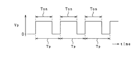
- FIG. 6 is a time chart showing an example of the pulse generated by the pulse generator.
- FIG. 7 is a configuration diagram of a temperature detection device according to another embodiment.
- the temperature detection device according to the present embodiment is mounted on a vehicle such as an electric vehicle or a hybrid vehicle, for example.
- the temperature detection device 20 detects the temperature of the assembled battery 10 mounted on the vehicle.
- the assembled battery 10 is composed of a series connection body of a plurality of battery modules 11, and each battery module 11 is composed of a series connection body of a plurality of cell cells 12.
- the temperature detection device 20 constitutes a battery monitoring device that monitors the state of the assembled battery 10.
- the assembled battery 10 includes a plurality of (n) temperature sensors 15.
- each temperature sensor 15 is individually provided corresponding to each battery module 11 and detects the temperature of each battery module 11.
- a thermistor is used as the temperature sensor 15.
- FIG. 1 shows a configuration in which one temperature sensor 15 is provided corresponding to each battery module 11, but the present invention is not limited to this. For example, two or more temperature sensors may be provided corresponding to each battery module 11.
- the temperature detection device 20 includes a constant voltage power supply 30 and a resistor 31.
- the first end of the resistor 31 is connected to the constant voltage power supply 30, and the first end of the temperature sensor 15 is connected to the second end of the resistor 31.
- a ground is connected to the second end of the temperature sensor 15.
- the constant voltage power supply 30 is shared by each temperature sensor 15.
- the temperature detection device 20 includes a multiplexer 40.
- the multiplexer 40 sequentially switches the input unit connected to the output unit OUT from the input units CH1 to CHn at a predetermined cycle.
- Each of the input units CH1 to CHn is connected to the first end of the temperature sensor 15 and the second end of the resistor 31. As a result, the voltage of the constant voltage power supply 30 divided by the temperature sensor 15 and the resistor 31 is input to each of the input units CH1 to CHn.
- the temperature detection device 20 includes a filter circuit 50.
- the filter circuit 50 is an RC low-pass filter circuit including a capacitor 51 and a filter resistor 52.
- the output unit OUT of the multiplexer 40 is connected to the first end of the filter resistor 52, and the first end of the capacitor 51 is connected to the second end of the filter resistor 52.
- a ground is connected to the second end of the capacitor 51.
- the filter circuit 50 removes noise from the output voltage of the output unit OUT.
- the temperature detection device 20 includes an A / D conversion unit 60, a microcomputer 61, and a storage unit 62.
- the input side of the A / D conversion unit 60 is connected to the filter circuit 50, and the output side is connected to the microcomputer 61.
- the A / D conversion unit 60 digitally converts the analog signal output from the filter circuit 50 and outputs it to the microcomputer 61. That is, the microcomputer 61 detects the output voltage of the filter circuit 50 based on the output signal of the A / D conversion unit.
- the microcomputer 61 operates the multiplexer 40 in order to sequentially switch the input unit connected to the output unit OUT from the input units CH1 to CHn at a predetermined cycle. Specifically, the microcomputer 61 switches the input unit connected to the output unit OUT in order from the first input unit CH1 to the nth input unit CHn in one cycle, and again in the next cycle, the input connected to the output unit OUT. The unit is switched in order from the first input unit CH1 to the nth input unit CHn.
- the open state is, for example, a state in which the output unit OUT is connected to the n + 1th input unit CHn + 1 when the temperature sensor 15 is not assigned to the n + 1 input unit CHn + 1 of the multiplexer 40.
- the microcomputer 61 corresponds to the "detection unit” and the "operation unit”.
- the microcomputer 61 operates the multiplexer 40 to detect and detect the first to nth output voltages V1 to Vn of the filter circuit 50 when the first to nth input units CH1 to CHn are connected to the output unit OUT. Based on the first to nth output voltages V1 to Vn, the temperature of the battery module 11 to be the temperature detection target of each temperature sensor 15 is detected. Further, the microcomputer 61 stores the detected first to nth output voltages V1 to Vn in the storage unit 62 in association with the first to nth input units CH1 to CHn.
- the storage unit 62 is a non-transitional substantive recording medium other than the ROM (for example, a non-volatile memory other than the ROM).
- the temperature detection device 20 includes a D / A converter 70 corresponding to a “charge / discharge unit” and a switch 71 as a connection unit.
- the switch 71 is provided in an electric path connecting the D / A converter 70 and the first end of the capacitor 51, and is turned on or off by the microcomputer 61. When the switch 71 is turned on, the D / A converter 70 and the capacitor 51 are electrically connected. On the other hand, when the switch 71 is turned off, the D / A converter 70 and the capacitor 51 are electrically cut off.
- the microcomputer 61 sets the target voltage Vt of the D / A converter 70, and controls the output voltage of the D / A converter 70 to the set target voltage Vt.
- a configuration is adopted in which the temperature detection cycle of each battery module 11 by the microcomputer 61 can be shortened.
- a configuration that shortens the temperature detection cycle is adopted, for example, for the reasons described below. That is, as the assembled battery 10, an assembled battery composed of a versatile storage battery such as a storage battery of 18650 may be used instead of a dedicated product for a vehicle. In this case, since the assembled battery 10 is not a dedicated product, it is desired to increase the number of temperature detection points of the assembled battery 10 in order to improve safety. In this case, it is required to shorten the temperature detection cycle in one cycle for temperature detection using the multiplexer 40.
- the temperature detection process executed by the microcomputer 61 will be described with reference to FIG.
- the situation in which the negative determination is made in step S10 is, for example, the situation in which the temperature detection process is first executed after the microcomputer 61 is started.
- step S10 If it is determined in step S10 that the jth output voltage Vj of the previous cycle is not stored, the process proceeds to step S11, and the multiplexer 40 is operated to connect the jth input unit and the output unit OUT.
- step S12 the process waits until the first specified period T1 elapses after the jth input unit CHj is connected to the output unit OUT.
- the first specified period T1 is a period of waiting for stabilization until the voltage Vc of the capacitor 51 becomes the input voltage of the jth input unit CHj or its vicinity.
- step S12 If it is determined in step S12 that the first specified period T1 has elapsed, the process proceeds to step S13, and the jth output voltage Vj is detected in this cycle. Then, the detected j-th output voltage Vj is stored in the storage unit 62 in association with the j-th input unit CHj.
- step S14 the multiplexer 40 is switched to the open state.
- step S15 it is determined whether or not the variable j is n. This process is for determining whether or not one cycle of temperature detection has been completed. If a negative determination is made in step S15, it is determined that one cycle has not been completed, and the process proceeds to step S16. In step S16, the variable j is incremented by 1, and then the process proceeds to step S10. On the other hand, when it is determined in step S15 that the variable j is n, it is determined that one cycle has been completed, the process proceeds to step S10, and the process proceeds to the next cycle.
- step S10 If it is determined in step S10 that the jth output voltage Vj (corresponding to the "target output voltage") of the previous cycle is stored, the process proceeds to step S18, and the jth output voltage Vj of the previous cycle is stored in the storage unit. Obtained from 62.
- step S19 the switch 71 is switched on. As a result, the D / A converter 70 and the capacitor 51 are electrically connected.
- step S20 the D / A converter 70 is operated in order to control the output voltage of the D / A converter 70 to the target voltage Vt.
- the target voltage Vt is set to the same voltage as the jth output voltage Vj of the previous cycle acquired in step S18.
- the capacitor 51 is charged by controlling the output voltage of the D / A converter 70, and the voltage Vc of the capacitor 51 rises toward the target voltage Vt.
- the capacitor 51 is discharged by controlling the output voltage of the D / A converter 70, and the voltage Vc of the capacitor 51 drops toward the target voltage Vt.
- step S21 the process waits until the second specified period T2 elapses after the control of the output voltage of the D / A converter 70 to the target voltage Vt is started.
- the process of step S21 is a process for determining whether or not the voltage Vc of the capacitor 51 has reached the target voltage Vt.
- the second specified period T2 is set to a shorter period than the first specified period T1.
- step S21 If it is determined in step S21 that the second specified period T2 has elapsed, the process proceeds to step S22 and the switch 71 is switched off.
- step S23 the jth input unit CHj (corresponding to the “target input unit”) and the output unit OUT are connected by operating the multiplexer 40.
- step S24 the process waits until the third specified period T3 elapses after the jth input unit CHj and the output unit OUT are connected.
- the process of step S24 is a process for determining whether or not the voltage Vc of the capacitor 51 has become the input voltage of the jth input unit CHj.
- the third specified period T3 is set to a shorter period than the first specified period T1.
- the added value of the second specified period T2 and the third specified period T3 is set to a period shorter than the first specified period T1.
- step S24 If it is determined in step S24 that the third specified period T3 has elapsed, the process proceeds to step S13, and the jth output voltage Vj is detected in this cycle. Then, the detected j-th output voltage Vj is stored in the storage unit 62 in association with the j-th input unit CHj.
- FIG. 3A shows the transition of the operating state of the multiplexer 40
- FIG. 3B shows the transition of the operating state of the switch 71
- FIG. 3C shows the transition of the operating state of the D / A converter 70
- FIG. 3D shows the transition of the voltage Vc of the capacitor 51.
- the example shown in FIG. 3 is a case where the connection target to the output unit OUT is switched from the first input unit CH1 to the second input unit CH2.
- the first input unit CH1 is disconnected from the output unit OUT, and the multiplexer 40 is opened.
- the switch 71 is switched on, and at time t3, the D / A converter 70 is operated in order to reduce the voltage Vc of the capacitor 51 to the target voltage Vt.
- This target voltage Vt is set to the second output voltage V2 in the previous cycle.
- the second input unit CH2 is connected to the output unit OUT. Then, at the time t7 when the third specified period T3 has elapsed from the time t6, the voltage Vc of the capacitor 51 is detected as the second output voltage V2 in this cycle.
- the voltage Vc of the capacitor 51 is set to the second output voltage V2 in the previous cycle. Therefore, the difference between the voltage Vc of the capacitor 51 at time t6 and the input voltage of the second input unit CH2 in this cycle can be reduced. As a result, the third specified period T3 for waiting for stability can be set to a short period, and the temperature detection cycle can be shortened.
- a comparative example is a configuration in which the D / A converter 70 and the switch 71 are removed from the configuration shown in FIG. 4 (a) and 4 (b) correspond to FIGS. 3 (a) and 3 (d) above.
- the broken line in FIG. 4B shows the transition of the voltage Vc of the capacitor 51 according to the present embodiment shown in FIG. 3D.
- the first input unit CH1 is disconnected from the output unit OUT, and the multiplexer 40 is opened.
- the second input unit CH2 is connected to the output unit OUT, and at time t3 when the first specified period T1 elapses from time t2, the voltage Vc of the capacitor 51 is set as the second output voltage V2 in this cycle. Detected.
- the temperature detection cycle since it is necessary to set the first specified period T1 for a long time in order to wait for the voltage Vc of the capacitor 51 to stabilize, the temperature detection cycle becomes long.
- the voltage of the capacitor 51 Vc can be brought close to the output voltage of the temperature sensor 15 input to the input unit after switching.
- the waiting time until the voltage Vc of the capacitor 51 becomes equal to the output voltage of the temperature sensor 15 after switching can be shortened, and the temperature detection cycle of the battery module 11 can be shortened.
- the target voltage Vt is set to the same voltage as the jth output voltage Vj of the previous cycle, the effect of shortening the temperature detection cycle can be enhanced.
- the temperature detection device 20 includes a pulse generator 72 instead of the D / A converter 70.
- the same components as those shown in FIG. 1 above are designated by the same reference numerals for convenience.
- the pulse generator 72 controls the voltage Vc of the capacitor 51 to the target voltage Vt set to the same voltage as the jth output voltage Vj of the previous cycle.
- the process of manipulating the generated pulse width Ton is performed.
- the pulse width Ton is defined as an output period of a predetermined voltage in the pulse generation cycle Tp.
- the pulse width Ton is larger than the reference width Ts ( ⁇ Tp)
- the larger the pulse width Ton the greater the degree of increase in the voltage Vc of the capacitor 51
- the pulse width Ton is smaller than the reference width Ts, the pulse width.
- the smaller the ton the greater the degree of decrease in the voltage Vc of the capacitor 51.
- a capacitor 32 for static electricity countermeasures may be connected between the first end of the temperature sensor 15 and each input portion CHj of the multiplexer 40.
- the same reference numerals are given to the same configurations as those shown in FIG. 1 above for convenience.
- the capacitor 51 constituting the filter circuit 50 is used. It will also serve as a capacitor for static electricity countermeasures. As a result, there is a concern that restrictions will be imposed on the setting of the capacity of the capacitor with an emphasis on measures against static electricity.
- the capacity of the capacitor 32 with an emphasis on measures against static electricity can be freely set.
- the configuration shown in FIG. 5 of the second embodiment may also be provided with the capacitor 32 for static electricity countermeasures.
- the target voltage Vt is not limited to the same voltage as the j output voltage Vj of the previous cycle, but is not limited to the j output voltage Vj of the cycle two times before, for example, the j output voltage Vj of the cycle two times before. It may be set to the same voltage.
- the target voltage Vt is not limited to the same voltage as the jth output voltage Vj of the previous cycle, and the j-1 input unit CHj-1 selected immediately before the jth input unit CHj in this cycle is the output unit. It may be set to a voltage between the output voltage of the filter circuit 50 when connected to OUT and the jth output voltage Vj of the previous cycle. Even in this case, the effect of shortening the temperature detection cycle can be obtained.
- the filter circuit may be, for example, an LC low-pass filter circuit instead of the RC low-pass filter circuit.
- the first end of the capacitor constituting the LC low-pass filter circuit is connected to the output unit OUT, and the second end of the capacitor is connected to the ground.
- the first end of the inductor constituting the LC low-pass filter circuit is connected to the first end of the capacitor, and the second end of the inductor is connected to the A / D conversion unit 60.
- the filter circuit is not limited to the low-pass filter circuit, and may be, for example, a band-pass filter circuit.
- Examples of this circuit include a bandpass filter circuit including a pair of capacitors and a pair of inductors.
- the assembled battery 10 may be configured by a parallel connection of a plurality of battery modules 11, or may be configured by a series connection of a plurality of battery modules 11 connected in parallel.
- the temperature sensor is not limited to the thermistor, and may be, for example, a temperature sensitive diode.
- the temperature detector is not limited to the one installed in the vehicle.
- the controls and methods thereof described in the present disclosure are provided by a dedicated computer provided by configuring a processor and memory programmed to perform one or more functions embodied by a computer program. It may be realized. Alternatively, the controls and methods thereof described in the present disclosure may be implemented by a dedicated computer provided by configuring the processor with one or more dedicated hardware logic circuits. Alternatively, the control unit and method thereof described in the present disclosure may be a combination of a processor and memory programmed to perform one or more functions and a processor composed of one or more hardware logic circuits. It may be realized by one or more dedicated computers configured. Further, the computer program may be stored in a computer-readable non-transitional tangible recording medium as an instruction executed by the computer.
Landscapes
- Physics & Mathematics (AREA)
- General Physics & Mathematics (AREA)
- Engineering & Computer Science (AREA)
- Manufacturing & Machinery (AREA)
- Chemical & Material Sciences (AREA)
- Chemical Kinetics & Catalysis (AREA)
- Electrochemistry (AREA)
- General Chemical & Material Sciences (AREA)
- Nonlinear Science (AREA)
- Secondary Cells (AREA)
- Measuring Temperature Or Quantity Of Heat (AREA)
Abstract
温度検出装置は、複数の温度センサ(15)ごとに個別に割り当てられる入力部(CHj)と、各入力部に共通の出力部(OUT)とを有し、各入力部の中から出力部に接続する入力部を順次切り替えるマルチプレクサ(40)と、出力部に接続され、コンデンサ(51)を有するフィルタ回路(50)と、フィルタ回路の出力電圧に基づいて、温度センサの温度検出対象の温度を検出する検出部(61)と、各入力部のうち出力部に接続される入力部を他の入力部に切り替える際に、コンデンサの充放電を行う充放電部(70,72)と、を備える。
Description
本出願は、2020年3月10日に出願された日本出願番号2020-041030号に基づくもので、ここにその記載内容を援用する。
本開示は、温度センサの出力電圧に基づいて温度検出対象の温度を検出する温度検出装置に関するものである。
この種の装置としては、特許文献1に記載されているように、マルチプレクサと、RCフィルタ回路とを備えるものが知られている。マルチプレクサは、複数の温度センサごとに個別に割り当てられる入力部と、各入力部に共通の出力部とを有し、各入力部の中から出力部に接続する入力部を順次切り替える。RCフィルタ回路は、出力部に接続され、コンデンサを有している。温度検出装置は、RCフィルタ回路の出力電圧に基づいて、温度センサの温度検出対象の温度を検出する。
特許文献1に記載の構成では、マルチプレクサの出力部に、RCフィルタ回路を構成するコンデンサが接続されている。このため、各入力部のうち出力部に接続される入力部が他の入力部に切り替えられると、切り替え前後の温度センサの出力電圧が異なることに起因して、コンデンサの電圧が切り替え後の温度センサの出力電圧と等しくなるまでの待ち時間が必要となる。その結果、温度検出対象の温度検出周期が長くなる懸念がある。特に、ノイズ除去効果を大きくするためにコンデンサの容量が大きくされる場合、待ち時間が顕著に長くなり、温度検出周期が過度に長くなる懸念がある。
なお、RCフィルタ回路を備える温度検出装置に限らず、コンデンサを有するフィルタ回路を備える温度検出装置であれば、上述した課題は同様に生じ得る。
本開示は、上記課題に鑑みてなされたものであり、その主たる目的は、温度検出周期を短縮できる温度検出装置を提供することにある。
本開示は、複数の温度センサごとに個別に割り当てられる入力部と、前記各入力部に共通の出力部とを有し、前記各入力部の中から前記出力部に接続する入力部を順次切り替えるマルチプレクサと、
前記出力部に接続され、コンデンサを有するフィルタ回路と、
前記フィルタ回路の出力電圧に基づいて、前記温度センサの温度検出対象の温度を検出する検出部と、
前記各入力部のうち前記出力部に接続される入力部を他の入力部に切り替える際に、前記コンデンサの充放電を行う充放電部と、を備える。
前記出力部に接続され、コンデンサを有するフィルタ回路と、
前記フィルタ回路の出力電圧に基づいて、前記温度センサの温度検出対象の温度を検出する検出部と、
前記各入力部のうち前記出力部に接続される入力部を他の入力部に切り替える際に、前記コンデンサの充放電を行う充放電部と、を備える。
本開示は、各入力部の中から出力部に接続する入力部を他の入力部に切り替える際に、コンデンサの充放電を行う充放電部を備えている。このため、切り替え前後で各入力部に入力される温度センサの出力電圧が異なっていたとしても、コンデンサの電圧を、切り替え後に入力部に入力される温度センサの出力電圧に近づけることができる。これにより、コンデンサの電圧が切り替え後の温度センサの出力電圧と等しくなるまでの待ち時間を短縮することができ、ひいては温度検出対象の温度検出周期を短縮することができる。
本開示についての上記目的およびその他の目的、特徴や利点は、添付の図面を参照しながら下記の詳細な記述により、より明確になる。その図面は、
図1は、第1実施形態に係る温度検出装置の構成図であり、
図2は、温度検出処理のフローチャートであり、
図3は、温度検出処理の一例を示すタイムチャートであり、
図4は、比較例に係る温度検出処理を示すタイムチャートであり、
図5は、第2実施形態に係る温度検出装置の構成図であり、
図6は、パルス発生器が発生するパルスの一例を示すタイムチャートであり、
図7は、その他の実施形態に係る温度検出装置の構成図である。
<第1実施形態>
以下、本開示に係る温度検出装置を具体化した第1実施形態について、図面を参照しつつ説明する。本実施形態に係る温度検出装置は、例えば、電気自動車やハイブリッド自動車等の車両に搭載される。
以下、本開示に係る温度検出装置を具体化した第1実施形態について、図面を参照しつつ説明する。本実施形態に係る温度検出装置は、例えば、電気自動車やハイブリッド自動車等の車両に搭載される。
図1に示すように、温度検出装置20は、車両に搭載された組電池10の温度を検出する。組電池10は、複数の電池モジュール11の直列接続体で構成され、各電池モジュール11は、複数の単電池12の直列接続体で構成されている。なお、本実施形態において、温度検出装置20は、組電池10の状態を監視する電池監視装置を構成する。
組電池10は、複数(n個)の温度センサ15を備えている。本実施形態において、各温度センサ15は、各電池モジュール11に対応して個別に設けられ、各電池モジュール11の温度を検出する。本実施形態では、温度センサ15として、サーミスタが用いられている。なお、図1には、各電池モジュール11に対応して1つの温度センサ15が設けられる構成を示したがこれに限らない。例えば、各電池モジュール11に対応して2つ以上の温度センサが設けられる構成であってもよい。
温度検出装置20は、定電圧電源30と、抵抗体31とを備えている。定電圧電源30には、抵抗体31の第1端が接続され、抵抗体31の第2端には、温度センサ15の第1端が接続されている。温度センサ15の第2端には、グランドが接続されている。なお、本実施形態では、定電圧電源30が各温度センサ15で共通化されている。
温度検出装置20は、マルチプレクサ40を備えている。マルチプレクサ40は、各温度センサ15に対応して個別に割り当てられる第j入力部CHj(j=1,2,…,n)と、各入力部CH1~CHnに共通の出力部OUTとを有している。マルチプレクサ40は、各入力部CH1~CHnの中から出力部OUTに接続する入力部を所定の周期で順次切り替える。各入力部CH1~CHnは、温度センサ15の第1端及び抵抗体31の第2端に接続されている。これにより、温度センサ15及び抵抗体31で分圧された定電圧電源30の電圧が各入力部CH1~CHnに入力される。
温度検出装置20は、フィルタ回路50を備えている。本実施形態において、フィルタ回路50は、コンデンサ51及びフィルタ抵抗体52を備えるRCローパスフィルタ回路である。詳しくは、フィルタ抵抗体52の第1端には、マルチプレクサ40の出力部OUTが接続され、フィルタ抵抗体52の第2端には、コンデンサ51の第1端が接続されている。コンデンサ51の第2端には、グランドが接続されている。フィルタ回路50は、出力部OUTの出力電圧からノイズを除去する。
温度検出装置20は、A/D変換部60、マイコン61及び記憶部62を備えている。A/D変換部60は、入力側がフィルタ回路50に接続され、出力側がマイコン61に接続されている。A/D変換部60は、フィルタ回路50から出力されたアナログ信号をデジタル変換してマイコン61に出力する。つまり、マイコン61は、A/D変換部の出力信号に基づいて、フィルタ回路50の出力電圧を検出する。
マイコン61は、各サイクルにおいて、各入力部CH1~CHnの中から出力部OUTに接続する入力部を所定の周期で順次切り替えるべく、マルチプレクサ40を操作する。詳しくは、マイコン61は、1つのサイクルにおいて、出力部OUTに接続する入力部を第1入力部CH1から第n入力部CHnまで順に切り替え、次のサイクルにおいて、再度、出力部OUTに接続する入力部を第1入力部CH1から第n入力部CHnまで順に切り替える。
ここで、出力部OUTから第i入力部CHi(i=1,2,…,5)が切り離されてから出力部OUTに第i+1入力部CHi+1が接続されるまでの期間は、出力部OUTに第1~第n入力部CH1~CHnのいずれも接続されないオープン状態の期間とされる。また、出力部OUTから第6入力部CH6が切り離されてから出力部OUTに第1入力部CH1が接続されるまでの期間もオープン状態の期間とされる。なお、オープン状態は、例えば、マルチプレクサ40の第n+1入力部CHn+1に温度センサ15が割り当てられていない場合において、出力部OUTが第n+1入力部CHn+1に接続される状態である。また、本実施形態において、マイコン61が「検出部」及び「操作部」に相当する。
マイコン61は、マルチプレクサ40を操作し、第1~第n入力部CH1~CHnが出力部OUTに接続された場合のフィルタ回路50の第1~第n出力電圧V1~Vnを検出し、検出した第1~第n出力電圧V1~Vnに基づいて、各温度センサ15の温度検出対象となる電池モジュール11の温度を検出する。また、マイコン61は、検出した第1~第n出力電圧V1~Vnを第1~第n入力部CH1~CHnと対応付けて記憶部62に記憶させる。記憶部62は、ROM以外の非遷移的実体的記録媒体(例えば、ROM以外の不揮発性メモリ)である。
温度検出装置20は、「充放電部」に相当するD/Aコンバータ70と、接続部としてのスイッチ71とを備えている。スイッチ71は、D/Aコンバータ70とコンデンサ51の第1端とを接続する電気経路に設けられ、マイコン61によりオン又はオフされる。スイッチ71がオンされると、D/Aコンバータ70とコンデンサ51とが電気的に接続される。一方、スイッチ71がオフされると、D/Aコンバータ70とコンデンサ51とが電気的に遮断される。
マイコン61は、D/Aコンバータ70の目標電圧Vtを設定し、設定した目標電圧VtにD/Aコンバータ70の出力電圧を制御する。
本実施形態では、マイコン61による各電池モジュール11の温度検出周期を短縮できる構成が採用されている。温度検出周期を短縮する構成は、例えば以下に説明する理由で採用される。つまり、組電池10として、車両用の専用品ではなく、18650の蓄電池等、汎用性のある蓄電池で構成された組電池が用いられることがある。この場合、組電池10が専用品でないことから、安全性を高めるために組電池10の温度検出箇所を増やすことが望まれる。この場合、マルチプレクサ40を用いた温度検出のための1サイクルにおいて、温度検出周期を短縮することが要求される。
図2を用いて、マイコン61により実行される温度検出処理について説明する。
ステップS10では、前回のサイクルの第j出力電圧Vj(j=1,2,…,n)が記憶部62に記憶されているか否かを判定する。なお、ステップS10で否定判定される状況は、例えば、マイコン61が起動されてから温度検出処理が最初に実施される状況である。
ステップS10において前回のサイクルの第j出力電圧Vjが記憶されていないと判定した場合には、ステップS11に進み、マルチプレクサ40を操作することにより第j入力部と出力部OUTとを接続する。
ステップS12では、第j入力部CHjが出力部OUTに接続されてから第1規定期間T1経過するまで待機する。第1規定期間T1は、コンデンサ51の電圧Vcが第j入力部CHjの入力電圧又はその電圧近傍になるまでの安定待ちの期間である。
ステップS12において第1規定期間T1経過したと判定した場合には、ステップS13に進み、今回のサイクルにおいて第j出力電圧Vjを検出する。そして、検出した第j出力電圧Vjを第j入力部CHjと対応付けて記憶部62に記憶する。
ステップS14では、マルチプレクサ40をオープン状態に切り替える。
ステップS15では、変数jがnであるか否かを判定する。この処理は、温度検出の1サイクルが終了したか否かを判定するためのものである。ステップS15において否定判定した場合には、1サイクルが終了していないと判定し、ステップS16に進む。ステップS16では変数jを1インクリメントし、その後ステップS10に進む。一方、ステップS15において変数jがnであると判定した場合には、1サイクルが終了したと判定し、ステップS10に進み、次回のサイクルに移行する。
ステップS10において前回のサイクルの第j出力電圧Vj(「対象出力電圧」に相当)が記憶されていると判定した場合には、ステップS18に進み、前回のサイクルの第j出力電圧Vjを記憶部62から取得する。
ステップS19では、スイッチ71をオンに切り替える。これにより、D/Aコンバータ70とコンデンサ51とが電気的に接続される。
ステップS20では、D/Aコンバータ70の出力電圧を目標電圧Vtに制御すべく、D/Aコンバータ70を操作する。本実施形態では、目標電圧Vtを、ステップS18で取得した前回のサイクルの第j出力電圧Vjと同一の電圧に設定する。コンデンサ51の電圧Vcが目標電圧Vtよりも低い場合、D/Aコンバータ70の出力電圧の制御によりコンデンサ51が充電され、コンデンサ51の電圧Vcが目標電圧Vtに向かって上昇する。一方、コンデンサ51の電圧Vcが目標電圧Vtよりも高い場合、D/Aコンバータ70の出力電圧の制御によりコンデンサ51から放電され、コンデンサ51の電圧Vcが目標電圧Vtに向かって低下する。
ステップS21では、目標電圧VtへのD/Aコンバータ70の出力電圧の制御を開始してから第2規定期間T2が経過するまで待機する。ステップS21の処理は、コンデンサ51の電圧Vcが目標電圧Vtになったか否かを判定するための処理である。第2規定期間T2は、第1規定期間T1よりも短い期間に設定されている。
ステップS21において第2規定期間T2経過したと判定した場合には、ステップS22に進み、スイッチ71をオフに切り替える。
ステップS23では、マルチプレクサ40を操作することにより第j入力部CHj(「対象入力部」に相当)と出力部OUTとを接続する。
ステップS24では、第j入力部CHjと出力部OUTとが接続されてから第3規定期間T3が経過するまで待機する。ステップS24の処理は、コンデンサ51の電圧Vcが第j入力部CHjの入力電圧になったか否かを判定するための処理である。第3規定期間T3は、第1規定期間T1よりも短い期間に設定されている。特に本実施形態では、第2規定期間T2及び第3規定期間T3の加算値が、第1規定期間T1よりも短い期間に設定されている。
ステップS24において第3規定期間T3経過したと判定した場合には、ステップS13に進み、今回のサイクルにおいて第j出力電圧Vjを検出する。そして、検出した第j出力電圧Vjを第j入力部CHjと対応付けて記憶部62に記憶する。
図3のタイムチャートを用いて、温度検出処理について説明する。図3(a)はマルチプレクサ40の操作状態の推移を示し、図3(b)はスイッチ71の操作状態の推移を示す。図3(c)はD/Aコンバータ70の操作状態の推移を示し、図3(d)はコンデンサ51の電圧Vcの推移を示す。図3に示す例は、出力部OUTへの接続対象が第1入力部CH1から第2入力部CH2に切り替えられる場合のものである。
時刻t1において、出力部OUTから第1入力部CH1が切り離され、マルチプレクサ40がオープン状態とされる。
時刻t2においてスイッチ71がオンに切り替えられ、時刻t3において、コンデンサ51の電圧Vcを目標電圧Vtまで低下させるべく、D/Aコンバータ70が操作される。この目標電圧Vtは、前回のサイクルにおける第2出力電圧V2に設定されている。
時刻t2から第2規定期間T2経過した時刻t4において、D/Aコンバータ70の出力電圧の制御が停止され、時刻t5においてスイッチ71がオフに切り替えられる。
その後時刻t6において、第2入力部CH2が出力部OUTに接続される。そして、時刻t6から第3規定期間T3経過した時刻t7において、コンデンサ51の電圧Vcが今回のサイクルにおける第2出力電圧V2として検出される。
時刻t6において、コンデンサ51の電圧Vcが前回のサイクルにおける第2出力電圧V2にされている。このため、時刻t6におけるコンデンサ51の電圧Vcと、今回のサイクルにおける第2入力部CH2の入力電圧との差を小さくすることができる。その結果、安定待ちのための第3規定期間T3を短い期間に設定することができ、ひいては温度検出周期を短縮することができる。
これに対し、図4に示す比較例では、温度検出周期が長くなってしまう。比較例は、図1に示す構成から、D/Aコンバータ70及びスイッチ71を除いた構成である。図4(a),(b)は、先の図3(a),(d)に対応している。なお、図4(b)の破線は、図3(d)に示した本実施形態に係るコンデンサ51の電圧Vcの推移を示す。
比較例では、時刻t1において、出力部OUTから第1入力部CH1が切り離され、マルチプレクサ40がオープン状態とされる。その後、時刻t2において、出力部OUTに第2入力部CH2が接続され、時刻t2から、第1規定期間T1経過した時刻t3において、コンデンサ51の電圧Vcが今回のサイクルにおける第2出力電圧V2として検出される。比較例では、コンデンサ51の電圧Vcの安定待ちのために第1規定期間T1を長く設定する必要があるため、温度検出周期が長くなってしまう。
以上説明したように、本実施形態によれば、出力部OUTに接続される入力部の切り替え前後で各入力部に入力される温度センサ15の出力電圧が異なっていたとしても、コンデンサ51の電圧Vcを、切り替え後に入力部に入力される温度センサ15の出力電圧に近づけることができる。これにより、コンデンサ51の電圧Vcが切り替え後の温度センサ15の出力電圧と等しくなるまでの待ち時間を短縮することができ、ひいては電池モジュール11の温度検出周期を短縮することができる。
特に本実施形態では、目標電圧Vtが前回のサイクルの第j出力電圧Vjと同一の電圧に設定されるため、温度検出周期の短縮効果を高めることができる。
<第2実施形態>
以下、第2実施形態について、第1実施形態との相違点を中心に図面を参照しつつ説明する。本実施形態では、温度検出装置20は、図5に示すように、D/Aコンバータ70に代えて、パルス発生器72を備えている。なお、図5において、先の図1に示した構成と同一の構成については、便宜上、同一の符号を付している。
以下、第2実施形態について、第1実施形態との相違点を中心に図面を参照しつつ説明する。本実施形態では、温度検出装置20は、図5に示すように、D/Aコンバータ70に代えて、パルス発生器72を備えている。なお、図5において、先の図1に示した構成と同一の構成については、便宜上、同一の符号を付している。
マイコン61は、図2のステップS20の処理に代えて、コンデンサ51の電圧Vcを、前回サイクルの第j出力電圧Vjと同一の電圧に設定した目標電圧Vtに制御すべく、パルス発生器72が発生するパルス幅Tonを操作する処理を行う。パルス幅Tonは、図6に示すように、パルス発生周期Tpにおける所定電圧の出力期間として定義されている。例えば、パルス幅Tonが基準幅Ts(<Tp)よりも大きい場合、パルス幅Tonが大きいほどコンデンサ51の電圧Vcの上昇度合いが大きくなり、パルス幅Tonが基準幅Tsよりも小さい場合、パルス幅Tonが小さいほどコンデンサ51の電圧Vcの低下度合いが大きくなる。
以上説明した本実施形態によれば、第1実施形態と同様の効果を得ることができる。
<その他の実施形態>
なお、上記各実施形態は、以下のように変更して実施してもよい。
なお、上記各実施形態は、以下のように変更して実施してもよい。
・図7に示すように、温度センサ15の第1端とマルチプレクサ40の各入力部CHjとの間に、静電気対策用のコンデンサ32が接続されていてもよい。なお、図7において、先の図1に示した構成と同一の構成については、便宜上、同一の符号を付している。
図7に示す構成とは異なり、マルチプレクサ40の各入力部CHjと温度センサ15の第1端との間にフィルタ回路50が接続された構成の場合、そのフィルタ回路50を構成するコンデンサ51が、静電気対策用のコンデンサの役割を兼ねることとなる。その結果、静電気対策を重点に置いたコンデンサの容量の設定に制約が課される懸念がある。これに対し、フィルタ回路50がマルチプレクサ40の出力部OUTに接続された図7に示す構成によれば、静電気対策を重点に置いたコンデンサ32の容量を自由に設定できる。なお、第2実施形態の図5に示した構成にも、静電気対策用のコンデンサ32が設けられていてもよい。
・目標電圧Vtは、前回のサイクルの第j出力電圧Vjと同一の電圧に限らず、例えば、2回前のサイクルの第j出力電圧Vj等、数回前のサイクルの第j出力電圧Vjと同一の電圧に設定されてもよい。
・目標電圧Vtは、前回のサイクルの第j出力電圧Vjと同一の電圧に限らず、今回のサイクルにおいて第j入力部CHjの直前に選択された第j-1入力部CHj-1が出力部OUTに接続された場合のフィルタ回路50の出力電圧と、前回のサイクルの第j出力電圧Vjとの間の電圧に設定されてもよい。この場合であっても、温度検出周期の短縮効果を得ることはできる。
・フィルタ回路としては、RCローパスフィルタ回路に代えて、例えば、LCローパスフィルタ回路であってもよい。この場合、LCローパスフィルタ回路を構成するコンデンサの第1端が出力部OUTに接続されるとともに、コンデンサの第2端がグランドに接続される。また、LCローパスフィルタ回路を構成するインダクタの第1端がコンデンサの第1端に接続されるとともに、インダクタの第2端がA/D変換部60に接続される。
また、フィルタ回路としては、ローパスフィルタ回路に限らず、例えばバンドパスフィルタ回路であってもよい。この回路としては、例えば、一対のコンデンサと、一対のインダクタとを備えるバンドパスフィルタ回路が挙げられる。
・組電池10は、複数の電池モジュール11の並列接続体で構成されていてもよいし、複数の電池モジュール11の直列接続体が並列接続されて構成されていてもよい。
・温度センサとしては、サーミスタに限らず、例えば感温ダイオードであってもよい。
・温度検出装置は、車両に搭載されるものに限らない。
・本開示に記載の制御部及びその手法は、コンピュータプログラムにより具体化された一つ乃至は複数の機能を実行するようにプログラムされたプロセッサ及びメモリを構成することによって提供された専用コンピュータにより、実現されてもよい。あるいは、本開示に記載の制御部及びその手法は、一つ以上の専用ハードウエア論理回路によってプロセッサを構成することによって提供された専用コンピュータにより、実現されてもよい。もしくは、本開示に記載の制御部及びその手法は、一つ乃至は複数の機能を実行するようにプログラムされたプロセッサ及びメモリと一つ以上のハードウエア論理回路によって構成されたプロセッサとの組み合わせにより構成された一つ以上の専用コンピュータにより、実現されてもよい。また、コンピュータプログラムは、コンピュータにより実行されるインストラクションとして、コンピュータ読み取り可能な非遷移有形記録媒体に記憶されていてもよい。
本開示は、実施例に準拠して記述されたが、本開示は当該実施例や構造に限定されるものではないと理解される。本開示は、様々な変形例や均等範囲内の変形をも包含する。加えて、様々な組み合わせや形態、さらには、それらに一要素のみ、それ以上、あるいはそれ以下、を含む他の組み合わせや形態をも、本開示の範疇や思想範囲に入るものである。
Claims (9)
- 複数の温度センサ(15)ごとに個別に割り当てられる入力部(CHj)と、前記各入力部に共通の出力部(OUT)とを有し、前記各入力部の中から前記出力部に接続する入力部を順次切り替えるマルチプレクサ(40)と、
前記出力部に接続され、コンデンサ(51)を有するフィルタ回路(50)と、
前記フィルタ回路の出力電圧に基づいて、前記温度センサの温度検出対象の温度を検出する検出部(61)と、
前記各入力部のうち前記出力部に接続される入力部を他の入力部に切り替える際に、前記コンデンサの充放電を行う充放電部(70,72)と、を備える温度検出装置。 - 前記出力部に接続される前記入力部と対応付けて、前記検出部により検出された前記フィルタ回路の出力電圧を記憶する記憶部(62)と、
前記記憶部に記憶された出力電圧に基づいて目標電圧を設定し、設定した前記目標電圧に前記コンデンサの電圧を制御すべく、前記充放電部を操作する操作部(61)と、を備える請求項1に記載の温度検出装置。 - 前記マルチプレクサは、各サイクルにおいて、前記各入力部の中から前記出力部に接続する入力部を順次切り替え、
前記記憶部には、前回のサイクルにおいて前記各入力部の中から順次選択される対象入力部が前記出力部に接続される場合に、検出された前記フィルタ回路の出力電圧が前記対象入力部と対応付けられて記憶され、
前記操作部は、
前記記憶部に記憶された前回のサイクルの前記対象入力部に対応する出力電圧である対象出力電圧に基づいて、今回のサイクルの前記対象入力部に対応する前記目標電圧を設定し、
今回のサイクルのうち、前記各入力部の中から前記対象入力部の直前に選択される入力部が前記出力部から切り離されてから、前記対象入力部が前記出力部に接続されるまでの期間において、前記対象入力部に対応する前記目標電圧に前記コンデンサの電圧を制御すべく前記充放電部を操作する請求項2に記載の温度検出装置。 - 前記操作部は、今回のサイクルの前記対象入力部に対応する前記目標電圧を、今回のサイクルにおいて前記対象入力部の直前に選択された前記入力部が前記出力部に接続された場合の前記フィルタ回路の出力電圧と、前記対象出力電圧との間の電圧に設定する請求項3に記載の温度検出装置。
- 前記操作部は、今回のサイクルの前記対象入力部に対応する前記目標電圧を、前回のサイクルにおいて前記記憶部に記憶された前記対象入力部に対応する出力電圧と同一の電圧に設定する請求項3に記載の温度検出装置。
- 前記充放電部は、パルス発生器(72)である請求項1~5のいずれか1項に記載の温度検出装置。
- 前記充放電部は、D/Aコンバータ(70)である請求項1~5のいずれか1項に記載の温度検出装置。
- 前記温度センサの温度検出対象が、組電池(10)を構成する電池モジュール(11)である請求項1~7のいずれか1項に記載の温度検出装置。
- 前記フィルタ回路は、RCローパスフィルタ回路である請求項1~8のいずれか1項に記載の温度検出装置。
Applications Claiming Priority (2)
| Application Number | Priority Date | Filing Date | Title |
|---|---|---|---|
| JP2020041030A JP7276207B2 (ja) | 2020-03-10 | 2020-03-10 | 温度検出装置 |
| JP2020-041030 | 2020-03-10 |
Publications (1)
| Publication Number | Publication Date |
|---|---|
| WO2021182012A1 true WO2021182012A1 (ja) | 2021-09-16 |
Family
ID=77672245
Family Applications (1)
| Application Number | Title | Priority Date | Filing Date |
|---|---|---|---|
| PCT/JP2021/005294 Ceased WO2021182012A1 (ja) | 2020-03-10 | 2021-02-12 | 温度検出装置 |
Country Status (2)
| Country | Link |
|---|---|
| JP (1) | JP7276207B2 (ja) |
| WO (1) | WO2021182012A1 (ja) |
Cited By (1)
| Publication number | Priority date | Publication date | Assignee | Title |
|---|---|---|---|---|
| EP4310472A1 (en) * | 2022-07-18 | 2024-01-24 | ABB E-Mobility B.V. | Temperature measurement arrangement in a power module |
Families Citing this family (1)
| Publication number | Priority date | Publication date | Assignee | Title |
|---|---|---|---|---|
| KR102814291B1 (ko) * | 2021-10-15 | 2025-05-28 | 주식회사 엘지에너지솔루션 | 노이즈 저감 회로 및 이를 포함하는 배터리 관리 장치 |
Citations (9)
| Publication number | Priority date | Publication date | Assignee | Title |
|---|---|---|---|---|
| US4217645A (en) * | 1979-04-25 | 1980-08-12 | Barry George H | Battery monitoring system |
| JPH06338798A (ja) * | 1985-09-06 | 1994-12-06 | Sony Tektronix Corp | 低域通過フィルタ装置 |
| JPH10261962A (ja) * | 1997-03-19 | 1998-09-29 | Nec Corp | A/dコンバータ |
| JPH11191735A (ja) * | 1994-01-19 | 1999-07-13 | Japan Radio Co Ltd | Pllシンセサイザ及びその制御方法 |
| JP2005210182A (ja) * | 2004-01-20 | 2005-08-04 | Toshiba Corp | アナログ/デジタルコンバータおよびそれを搭載したマイクロコンピュータ |
| JP2005224071A (ja) * | 2004-02-09 | 2005-08-18 | Denso Corp | 電池制御装置 |
| JP2007089371A (ja) * | 2005-09-26 | 2007-04-05 | Pioneer Electronic Corp | バックコンバータ |
| JP2013058843A (ja) * | 2011-09-07 | 2013-03-28 | Denso Corp | 電子制御装置 |
| JP2017118180A (ja) * | 2015-12-21 | 2017-06-29 | 株式会社デンソー | A/d変換装置 |
-
2020
- 2020-03-10 JP JP2020041030A patent/JP7276207B2/ja active Active
-
2021
- 2021-02-12 WO PCT/JP2021/005294 patent/WO2021182012A1/ja not_active Ceased
Patent Citations (9)
| Publication number | Priority date | Publication date | Assignee | Title |
|---|---|---|---|---|
| US4217645A (en) * | 1979-04-25 | 1980-08-12 | Barry George H | Battery monitoring system |
| JPH06338798A (ja) * | 1985-09-06 | 1994-12-06 | Sony Tektronix Corp | 低域通過フィルタ装置 |
| JPH11191735A (ja) * | 1994-01-19 | 1999-07-13 | Japan Radio Co Ltd | Pllシンセサイザ及びその制御方法 |
| JPH10261962A (ja) * | 1997-03-19 | 1998-09-29 | Nec Corp | A/dコンバータ |
| JP2005210182A (ja) * | 2004-01-20 | 2005-08-04 | Toshiba Corp | アナログ/デジタルコンバータおよびそれを搭載したマイクロコンピュータ |
| JP2005224071A (ja) * | 2004-02-09 | 2005-08-18 | Denso Corp | 電池制御装置 |
| JP2007089371A (ja) * | 2005-09-26 | 2007-04-05 | Pioneer Electronic Corp | バックコンバータ |
| JP2013058843A (ja) * | 2011-09-07 | 2013-03-28 | Denso Corp | 電子制御装置 |
| JP2017118180A (ja) * | 2015-12-21 | 2017-06-29 | 株式会社デンソー | A/d変換装置 |
Cited By (1)
| Publication number | Priority date | Publication date | Assignee | Title |
|---|---|---|---|---|
| EP4310472A1 (en) * | 2022-07-18 | 2024-01-24 | ABB E-Mobility B.V. | Temperature measurement arrangement in a power module |
Also Published As
| Publication number | Publication date |
|---|---|
| JP7276207B2 (ja) | 2023-05-18 |
| JP2021143864A (ja) | 2021-09-24 |
Similar Documents
| Publication | Publication Date | Title |
|---|---|---|
| US7193390B2 (en) | Apparatus for connecting secondary battery cells in series and method for controlling secondary battery cells connected in series | |
| JP5980943B2 (ja) | 組電池監視装置 | |
| JP6986004B2 (ja) | 絶縁抵抗検出装置 | |
| JP5706739B2 (ja) | 電力変換システム | |
| US20200099110A1 (en) | Method of Managing Batteries and Power Supply System | |
| JP6136820B2 (ja) | 電池監視装置、蓄電装置および電池監視方法 | |
| WO2017217248A1 (ja) | パワーコンバータユニット | |
| WO2021182012A1 (ja) | 温度検出装置 | |
| US20200161968A1 (en) | Charge pump | |
| EP4130765B1 (en) | Ground fault detection device | |
| US10627453B2 (en) | Integrated circuit with built-in status monitoring unit and power supply device provided with said integrated circuit | |
| JP7033102B2 (ja) | 漏電判定装置 | |
| JP2018164323A (ja) | 車載用の制御装置及び車載用電源装置 | |
| JP6060804B2 (ja) | 組電池システム | |
| US11110817B2 (en) | Equalization control device and in-vehicle power supply device | |
| US20060044054A1 (en) | Midpoint potential generating circuit for use in a semiconductor device | |
| JP2009165265A (ja) | 電力変換装置 | |
| WO2018083851A1 (ja) | 電圧検出装置 | |
| JP4389758B2 (ja) | セル電圧バラツキ異常検出装置 | |
| JP2015095912A (ja) | 蓄電装置 | |
| JP6268357B1 (ja) | 蓄電装置及びその制御方法 | |
| US9882469B2 (en) | Booster apparatus for a direct current voltage generator | |
| JP7111052B2 (ja) | 燃料噴射弁駆動装置 | |
| KR101147500B1 (ko) | 전기이중층커패시터의 밸런서 | |
| JP3092275B2 (ja) | Dc−dcコンバータ |
Legal Events
| Date | Code | Title | Description |
|---|---|---|---|
| 121 | Ep: the epo has been informed by wipo that ep was designated in this application |
Ref document number: 21767737 Country of ref document: EP Kind code of ref document: A1 |
|
| NENP | Non-entry into the national phase |
Ref country code: DE |
|
| 122 | Ep: pct application non-entry in european phase |
Ref document number: 21767737 Country of ref document: EP Kind code of ref document: A1 |