WO2021111772A1 - 比較回路、半導体装置 - Google Patents
比較回路、半導体装置 Download PDFInfo
- Publication number
- WO2021111772A1 WO2021111772A1 PCT/JP2020/040385 JP2020040385W WO2021111772A1 WO 2021111772 A1 WO2021111772 A1 WO 2021111772A1 JP 2020040385 W JP2020040385 W JP 2020040385W WO 2021111772 A1 WO2021111772 A1 WO 2021111772A1
- Authority
- WO
- WIPO (PCT)
- Prior art keywords
- voltage
- circuit
- comparison circuit
- threshold voltage
- output
- Prior art date
- Legal status (The legal status is an assumption and is not a legal conclusion. Google has not performed a legal analysis and makes no representation as to the accuracy of the status listed.)
- Ceased
Links
Images




Classifications
-
- H—ELECTRICITY
- H03—ELECTRONIC CIRCUITRY
- H03K—PULSE TECHNIQUE
- H03K5/00—Manipulating of pulses not covered by one of the other main groups of this subclass
- H03K5/22—Circuits having more than one input and one output for comparing pulses or pulse trains with each other according to input signal characteristics, e.g. slope, integral
- H03K5/24—Circuits having more than one input and one output for comparing pulses or pulse trains with each other according to input signal characteristics, e.g. slope, integral the characteristic being amplitude
- H03K5/2472—Circuits having more than one input and one output for comparing pulses or pulse trains with each other according to input signal characteristics, e.g. slope, integral the characteristic being amplitude using field effect transistors
- H03K5/2481—Circuits having more than one input and one output for comparing pulses or pulse trains with each other according to input signal characteristics, e.g. slope, integral the characteristic being amplitude using field effect transistors with at least one differential stage
-
- H—ELECTRICITY
- H03—ELECTRONIC CIRCUITRY
- H03K—PULSE TECHNIQUE
- H03K3/00—Circuits for generating electric pulses; Monostable, bistable or multistable circuits
- H03K3/02—Generators characterised by the type of circuit or by the means used for producing pulses
- H03K3/353—Generators characterised by the type of circuit or by the means used for producing pulses by the use, as active elements, of field-effect transistors with internal or external positive feedback
- H03K3/356—Bistable circuits
- H03K3/3565—Bistables with hysteresis, e.g. Schmitt trigger
-
- H—ELECTRICITY
- H03—ELECTRONIC CIRCUITRY
- H03K—PULSE TECHNIQUE
- H03K5/00—Manipulating of pulses not covered by one of the other main groups of this subclass
- H03K5/22—Circuits having more than one input and one output for comparing pulses or pulse trains with each other according to input signal characteristics, e.g. slope, integral
- H03K5/24—Circuits having more than one input and one output for comparing pulses or pulse trains with each other according to input signal characteristics, e.g. slope, integral the characteristic being amplitude
- H03K5/2472—Circuits having more than one input and one output for comparing pulses or pulse trains with each other according to input signal characteristics, e.g. slope, integral the characteristic being amplitude using field effect transistors
-
- G—PHYSICS
- G01—MEASURING; TESTING
- G01R—MEASURING ELECTRIC VARIABLES; MEASURING MAGNETIC VARIABLES
- G01R19/00—Arrangements for measuring currents or voltages or for indicating presence or sign thereof
- G01R19/165—Indicating that current or voltage is either above or below a predetermined value or within or outside a predetermined range of values
- G01R19/16533—Indicating that current or voltage is either above or below a predetermined value or within or outside a predetermined range of values characterised by the application
- G01R19/16538—Indicating that current or voltage is either above or below a predetermined value or within or outside a predetermined range of values characterised by the application in AC or DC supplies
-
- H—ELECTRICITY
- H02—GENERATION; CONVERSION OR DISTRIBUTION OF ELECTRIC POWER
- H02M—APPARATUS FOR CONVERSION BETWEEN AC AND AC, BETWEEN AC AND DC, OR BETWEEN DC AND DC, AND FOR USE WITH MAINS OR SIMILAR POWER SUPPLY SYSTEMS; CONVERSION OF DC OR AC INPUT POWER INTO SURGE OUTPUT POWER; CONTROL OR REGULATION THEREOF
- H02M1/00—Details of apparatus for conversion
- H02M1/08—Circuits specially adapted for the generation of control voltages for semiconductor devices incorporated in static converters
- H02M1/088—Circuits specially adapted for the generation of control voltages for semiconductor devices incorporated in static converters for the simultaneous control of series or parallel connected semiconductor devices
-
- H—ELECTRICITY
- H02—GENERATION; CONVERSION OR DISTRIBUTION OF ELECTRIC POWER
- H02M—APPARATUS FOR CONVERSION BETWEEN AC AND AC, BETWEEN AC AND DC, OR BETWEEN DC AND DC, AND FOR USE WITH MAINS OR SIMILAR POWER SUPPLY SYSTEMS; CONVERSION OF DC OR AC INPUT POWER INTO SURGE OUTPUT POWER; CONTROL OR REGULATION THEREOF
- H02M3/00—Conversion of DC power input into DC power output
- H02M3/02—Conversion of DC power input into DC power output without intermediate conversion into AC
- H02M3/04—Conversion of DC power input into DC power output without intermediate conversion into AC by static converters
- H02M3/10—Conversion of DC power input into DC power output without intermediate conversion into AC by static converters using discharge tubes with control electrode or semiconductor devices with control electrode
- H02M3/145—Conversion of DC power input into DC power output without intermediate conversion into AC by static converters using discharge tubes with control electrode or semiconductor devices with control electrode using devices of a triode or transistor type requiring continuous application of a control signal
- H02M3/155—Conversion of DC power input into DC power output without intermediate conversion into AC by static converters using discharge tubes with control electrode or semiconductor devices with control electrode using devices of a triode or transistor type requiring continuous application of a control signal using semiconductor devices only
- H02M3/156—Conversion of DC power input into DC power output without intermediate conversion into AC by static converters using discharge tubes with control electrode or semiconductor devices with control electrode using devices of a triode or transistor type requiring continuous application of a control signal using semiconductor devices only with automatic control of output voltage or current, e.g. switching regulators
- H02M3/158—Conversion of DC power input into DC power output without intermediate conversion into AC by static converters using discharge tubes with control electrode or semiconductor devices with control electrode using devices of a triode or transistor type requiring continuous application of a control signal using semiconductor devices only with automatic control of output voltage or current, e.g. switching regulators including plural semiconductor devices as final control devices for a single load
-
- H—ELECTRICITY
- H03—ELECTRONIC CIRCUITRY
- H03K—PULSE TECHNIQUE
- H03K17/00—Electronic switching or gating, i.e. not by contact-making and –breaking
- H03K17/30—Modifications for providing a predetermined threshold before switching
- H03K17/302—Modifications for providing a predetermined threshold before switching in field-effect transistor switches
-
- H—ELECTRICITY
- H03—ELECTRONIC CIRCUITRY
- H03K—PULSE TECHNIQUE
- H03K17/00—Electronic switching or gating, i.e. not by contact-making and –breaking
- H03K17/51—Electronic switching or gating, i.e. not by contact-making and –breaking characterised by the components used
- H03K17/56—Electronic switching or gating, i.e. not by contact-making and –breaking characterised by the components used by the use, as active elements, of semiconductor devices
- H03K17/687—Electronic switching or gating, i.e. not by contact-making and –breaking characterised by the components used by the use, as active elements, of semiconductor devices the devices being field-effect transistors
-
- H—ELECTRICITY
- H03—ELECTRONIC CIRCUITRY
- H03K—PULSE TECHNIQUE
- H03K19/00—Logic circuits, i.e. having at least two inputs acting on one output; Inverting circuits
- H03K19/02—Logic circuits, i.e. having at least two inputs acting on one output; Inverting circuits using specified components
- H03K19/08—Logic circuits, i.e. having at least two inputs acting on one output; Inverting circuits using specified components using semiconductor devices
- H03K19/094—Logic circuits, i.e. having at least two inputs acting on one output; Inverting circuits using specified components using semiconductor devices using field-effect transistors
- H03K19/0944—Logic circuits, i.e. having at least two inputs acting on one output; Inverting circuits using specified components using semiconductor devices using field-effect transistors using MOSFET or insulated gate field-effect transistors, i.e. IGFET
- H03K19/0948—Logic circuits, i.e. having at least two inputs acting on one output; Inverting circuits using specified components using semiconductor devices using field-effect transistors using MOSFET or insulated gate field-effect transistors, i.e. IGFET using CMOS or complementary insulated gate field-effect transistors
-
- H—ELECTRICITY
- H03—ELECTRONIC CIRCUITRY
- H03K—PULSE TECHNIQUE
- H03K3/00—Circuits for generating electric pulses; Monostable, bistable or multistable circuits
- H03K3/02—Generators characterised by the type of circuit or by the means used for producing pulses
- H03K3/353—Generators characterised by the type of circuit or by the means used for producing pulses by the use, as active elements, of field-effect transistors with internal or external positive feedback
-
- H—ELECTRICITY
- H03—ELECTRONIC CIRCUITRY
- H03K—PULSE TECHNIQUE
- H03K2217/00—Indexing scheme related to electronic switching or gating, i.e. not by contact-making or -breaking covered by H03K17/00
- H03K2217/0063—High side switches, i.e. the higher potential [DC] or life wire [AC] being directly connected to the switch and not via the load
-
- H—ELECTRICITY
- H03—ELECTRONIC CIRCUITRY
- H03K—PULSE TECHNIQUE
- H03K2217/00—Indexing scheme related to electronic switching or gating, i.e. not by contact-making or -breaking covered by H03K17/00
- H03K2217/0072—Low side switches, i.e. the lower potential [DC] or neutral wire [AC] being directly connected to the switch and not via the load
-
- H—ELECTRICITY
- H03—ELECTRONIC CIRCUITRY
- H03K—PULSE TECHNIQUE
- H03K2217/00—Indexing scheme related to electronic switching or gating, i.e. not by contact-making or -breaking covered by H03K17/00
- H03K2217/0081—Power supply means, e.g. to the switch driver
-
- H—ELECTRICITY
- H03—ELECTRONIC CIRCUITRY
- H03K—PULSE TECHNIQUE
- H03K3/00—Circuits for generating electric pulses; Monostable, bistable or multistable circuits
- H03K3/02—Generators characterised by the type of circuit or by the means used for producing pulses
- H03K3/027—Generators characterised by the type of circuit or by the means used for producing pulses by the use of logic circuits, with internal or external positive feedback
-
- H—ELECTRICITY
- H03—ELECTRONIC CIRCUITRY
- H03K—PULSE TECHNIQUE
- H03K5/00—Manipulating of pulses not covered by one of the other main groups of this subclass
- H03K5/01—Shaping pulses
- H03K5/08—Shaping pulses by limiting; by thresholding; by slicing, i.e. combined limiting and thresholding
Definitions
- the present invention relates to a comparison circuit and a semiconductor device.
- a comparison circuit using a Schmitt trigger circuit having a hysteresis characteristic is generally used (for example, Patent Document 1).
- the hysteresis characteristic is determined by the threshold voltage of the MOS transistor of the Schmitt trigger circuit, and it is difficult to change the hysteresis characteristic.
- the present invention has been made in view of the above-mentioned conventional problems, and an object of the present invention is to provide a comparison circuit in which the hysteresis characteristics can be changed.
- the comparison circuit of the present invention when the input voltage exceeds the first threshold voltage, the output voltage of the first logic level is output, and the input voltage becomes the first threshold.
- a comparison circuit that outputs the output voltage of the second logic level when the voltage falls below the second threshold voltage lower than the value voltage, and the input voltage is the first voltage and the second voltage lower than the first voltage.
- the first voltage exceeds the third threshold voltage
- the output voltage of the first logic level is output, and the second voltage becomes the third threshold.
- a logic circuit that outputs the output voltage of the second logic level when the voltage falls below the fourth threshold voltage lower than the value voltage is provided.
- the aspect of the semiconductor device of the present invention is a power supply circuit that generates a low power supply voltage lower than the power supply voltage from the power supply voltage, and a switching element of the upper arm and a switching element of the lower arm that operates at the low power supply voltage.
- a semiconductor device including a detection circuit for detecting a control signal for driving the device and a drive circuit for driving the switching element of the upper arm and the switching element of the lower arm based on the detection result of the detection circuit. When the voltage level of the control signal exceeds the first threshold voltage, the detection circuit outputs the detection result of the first logic level, and the voltage level of the control signal is the first threshold.
- a comparison circuit for outputting the detection result of the second logic level is provided, and the comparison circuit sets the voltage level of the control signal to the first voltage and the first voltage.
- a conversion circuit that converts to a second voltage lower than the first voltage, and when the first voltage exceeds the third threshold voltage, the detection result of the first logic level is output, and the second voltage becomes the second voltage.
- a logic circuit that outputs the detection result of the second logic level when the voltage falls below the fourth threshold voltage, which is lower than the third threshold voltage, is provided.
- FIG. 10 It is a figure which shows an example of the structure of a power module 10. It is a figure which shows an example of the structure of HVIC20. It is a figure which shows the structure of the comparison circuit 21a which is one Embodiment of the comparison circuit 21. It is a figure which shows an example of the structure of the logic circuit 50. It is a figure explaining the operation of the logic circuit 50. It is a figure which shows the change of the threshold value when the comparison circuit 21a is used. It is a figure which shows an example of the structure of the comparison circuit 21b. It is a figure which shows an example of the structure of the comparison circuit 21c.
- FIG. 1 is a diagram showing an example of a configuration of a power module 10 according to an embodiment of the present invention.
- the power module 10 is a semiconductor device that includes a power semiconductor for power conversion and a drive circuit, and drives, for example, a load 11.
- the power module 10 includes a capacitor 14, an HVIC 20, a bridge circuit 30, and terminals PWR, D, P, S, N, and COM for generating a bootstrap voltage Vb.
- a power supply voltage VCS is applied to the terminal PWR, and a control signal IN from an MCU (not shown) is input to the terminal D.
- a load 11 is connected between the terminal S and the terminal N.
- a power supply voltage Vdc is applied to the terminal P, and a capacitor 12 for stabilizing the power supply voltage Vdc is connected between the terminal P and the terminal N.
- the HVIC 20 receives the control signal IN from the MCU (not shown), outputs the drive signals HO and LO to the bridge circuit 30, and drives the bridge circuit 30.
- the bridge circuit 30 drives the load 11 (for example, an inductor) based on the drive signals HO and LO from the HVIC 20.
- the bridge circuit 30 includes the NMOS transistors 31 and 32.
- the NMOS transistors 31 and 32 correspond to "switching elements".
- FIG. 2 is a diagram showing an example of the configuration of the HVIC 20.
- the HVIC (High Voltage Integrated Circuit) 20 includes a comparison circuit 21, an inverter 22, a filter circuit 23, a pulse generation circuit 24, a high side drive circuit 25, a power supply circuit 26, a low side drive circuit 27, terminals PVCC, DS, VB, H, Includes VS, L, G.
- the comparison circuit 21 is an input detection circuit that detects the input control signal IN and inverts the control signal IN and outputs the control signal IN.
- the control signal IN changes, for example, in the range of 0 to 15V in the present embodiment. Therefore, the comparison circuit 21 is composed of a high withstand voltage element.
- the control signal IN is a rectangular wave that changes between 0 and 15 V, and in the case of a high level (hereinafter referred to as “H” level), the NMOS transistor 31 of the upper arm is turned on and the low level (hereinafter referred to as “H” level) is turned on. In the case of “L” level), the NMOS transistor 32 of the lower arm is turned on.
- the inverter 22 inverts the output of the comparison circuit 21 and outputs it to the filter circuit 23.
- the filter circuit 23 includes, for example, a low-pass filter (not shown) and outputs a signal S from which noise of the signal output from the inverter 22 is removed.
- the pulse generation circuit 24 generates a set signal set at the rising edge of the signal S and a reset signal reset at the falling edge.
- the high-side drive circuit 25 outputs a drive signal HO for driving the NMOS transistor 31 of the upper arm via the terminal H based on the set signal set and the reset signal reset from the pulse generation circuit 24.
- the power supply circuit 26 is, for example, a step-down regulator, steps down the power supply voltage VCS (for example, 15V) from the terminal PVCC to generate a low power supply voltage VDD (for example, 5V), and the comparison circuit 21 and the inverter 22. , The filter circuit 23 and the pulse generation circuit 24.
- VCS power supply voltage
- VDD low power supply voltage
- the low-side drive circuit 27 outputs a drive signal LO for driving the NMOS transistor 32 of the lower arm based on the signal S from the filter circuit 23 via the terminal L.
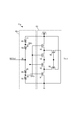
- FIG. 3 is a diagram showing a configuration of a comparison circuit 21a, which is an embodiment of the comparison circuit 21.
- the comparison circuit 21a when the voltage level of the control signal IN changes from a low voltage level (for example, 0V) to a high voltage level (for example, VDD) and exceeds the high threshold voltage VtH, the logic level of the output voltage Vout is changed to ". Change from "H” level to "L” level. Further, in the comparison circuit 21a, when the voltage level of the control signal IN changes from a high voltage level to a low voltage level and falls below the low threshold voltage VtL, the logic level of the output voltage Vout is changed from the “L” level to “H”. Change to a level.
- the comparison circuit 21a includes a voltage conversion circuit 40a and a logic circuit 50.
- the voltage conversion circuit 40a converts the voltage generated at the node N1 to which the control signal IN is input into a voltage VNG and a voltage VPG lower than the voltage VNG.
- the voltage generated at the node N1 will be referred to as an input voltage Vin.
- the voltage conversion circuit 40a includes resistors 41 to 44.
- the resistors 41 to 44 are connected in series between the node to which the low power supply voltage VDD is applied and the ground.
- the voltage conversion circuit 40a When the input voltage Vin is applied to the node N1, the voltage conversion circuit 40a generates a voltage VNG at the connection point between the resistor 41 and the resistor 42, and the voltage VPG at the connection point between the resistor 43 and the resistor 44. To generate.
- the voltage VNG is applied to the gate electrodes of the NMOS transistors 51 and 52, which are the inputs of the logic circuit 50, and the voltage VPG is applied to the gate electrodes of the MPa transistors 54, 55 of the logic circuit 50, which are the inputs of the logic circuit 50. Will be done.
- the voltage VNG and the voltage VPG are calculated as follows, where the resistance values of the resistors 41 to 44 are R1, R2, R3, and R4.
- the logic circuit 50 is a Schmitt trigger circuit that changes the logic level of the output voltage Vout with a hysteresis characteristic according to the change of the voltage levels of the voltages VNG and VPG.
- the logic circuit 50 is configured to include the NMOS transistors 51 to 53 and the MPa transistors 54 to 56.
- the NMOS transistors 51, 52 and the MIMO transistors 54, 55 are placed between the power supply node to which the low power supply voltage VDD is applied in series in the order of the MIMO transistors 55, 54 and the NMOS transistors 52, 51 from the power supply side and the ground. Connected to. Further, the voltage VNG is applied to the gate electrodes of the NMOS transistors 51 and 52, which are the inputs of the logic circuit 50, and the voltage VPG is applied to the gate electrodes of the PRIVATE transistors 54 and 55.
- the output voltage Vout output from the connection point between the NMOS transistor 52 and the epitaxial transistor 54 is applied to the gate electrode, and the low power supply voltage VDD is applied to the drain terminal.
- the source electrode is connected to the connection point.
- the output voltage Vout is applied to the gate electrode, the drain terminal is grounded, and the source electrode is connected to the connection points of the epitaxial transistors 54 and 55.
- the maximum value of the voltage of the control signal IN has a voltage higher than the power supply voltage of the logic circuit 50. Therefore, the NMOS transistors 51 to 53 and the NMOS transistors 54 to 56 are composed of high withstand voltage MOS transistors.
- the resistance values R1 to R4 turn off any pair of the MPa transistors 54 and 55 or the NMOS transistors 51 and 52 when the input voltage Vin is not applied to the node N1. It has a resistance value.
- the resistors 41 to 44 correspond to the "first resistor”, “second resistor”, “third resistor”, and “fourth resistor”, respectively.
- the voltage VNG corresponds to the "first voltage” and the voltage VPG corresponds to the "second voltage”.
- the NMOS transistors 51 and 52 correspond to “two NMOS transistors”
- the MIMO transistors 54 and 55 correspond to “two MIMO transistors”. Further, the logic level of the output voltage Vout corresponds to the "detection result”.
- the logic circuit 50 operates at a low power supply voltage VDD (for example, 5V) lower than the maximum value of the input voltage Vin (for example, 15V).
- VDD low power supply voltage
- Vin maximum value of the input voltage Vin
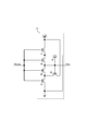
- FIG. 5 is a diagram illustrating the operation of the logic circuit 50. The operation of the NMOS transistors 51 to 53 and the MIMO transistors 54 to 56 of the logic circuit 50 will be described with reference to FIG.
- the straight line shown by the dotted line shows the relationship between the input voltage Vin_org input to the logic circuit 50 and the applied voltage applied to the gate electrodes of the NMOS transistors 51 and 52 and the MPa transistors 54 and 55.
- the input voltage Vin_org changes from X1 to X3
- the input voltage Vin_org is 0V.
- the NMOS transistors 51 and 52 are turned off, and the NMOS transistors 53 are turned on.
- the epitaxial transistors 54 and 55 are turned on, and the epitaxial transistors 56 are turned off. Therefore, the output voltage Vout is the power supply voltage VDD.
- the NMOS transistor 51 is turned on, the NMOS transistor 52 is turned off, and the NMOS transistor 53 is turned on.
- the epitaxial transistors 54 and 55 are turned off, and the epitaxial transistors 56 are turned off. Then, the output voltage Vout remains the power supply voltage VDD because the parasitic capacitance of the node to which the output voltage Vout is applied is still charged.
- the output voltage Vout changes from the power supply voltage VDD to 0V. Therefore, the voltage value of the input voltage Vin_org at this time becomes a high threshold voltage VtH_org.
- the input voltage Vin_org becomes the high threshold voltage VtH_org of the logic circuit 50
- the applied voltage applied to the gate electrodes of the NMOS transistors 51 and 52 becomes the voltage level indicated by the point A1 (that is, VtH_org).
- the output voltage Vout changes from the “H” level to the “L” level via the point A1.
- the input voltage Vin_org is higher than the power supply voltage VDD (for example, 15V).
- VDD for example, 15V.
- the NMOS transistors 51 and 52 are turned on, and the NMOS transistors 53 are turned off.
- the epitaxial transistors 54 and 55 are turned off, and the epitaxial transistors 56 are turned on. Therefore, the output voltage Vout remains 0V.
- the input voltage Vin_org becomes a voltage higher than the power supply voltage VDD (for example, 15V).
- VDD for example, 15V
- the epitaxial transistors 54 and 55 are turned off, and the epitaxial transistors 56 are turned on.
- the NMOS transistors 51 and 52 are turned on, and the NMOS transistors 53 are turned off. Therefore, the output voltage Vout becomes 0V.
- the epitaxial transistor 54 is turned off, the epitaxial transistor 55 is turned on, and the epitaxial transistor 56 is turned on.
- the NMOS transistors 51 and 52 are turned off, and the NMOS transistors 53 are turned off. Then, the output voltage Vout remains 0V because the parasitic capacitance of the node to which the output voltage Vout is applied remains discharged.
- the output voltage Vout changes from 0V to the power supply voltage VDD. Therefore, the voltage value of the input voltage Vin_org at this time is a low threshold voltage VtL_org.
- the input voltage Vin_org becomes the low threshold voltage VtL_org of the logic circuit 50
- the applied voltage applied to the gate electrodes of the epitaxial transistors 54 and 55 becomes the voltage level indicated by the point B1 (that is, VtL_org). At this time, the output voltage Vout changes from the “L” level to the “H” level via the point B1.
- the input voltage Vin_org becomes 0V.
- the epitaxial transistors 54 and 55 are turned on, and the epitaxial transistors 56 are turned off.
- the NMOS transistors 51 and 52 are turned off, and the NMOS transistor 53 is turned on. Therefore, the output voltage Vout remains the power supply voltage VDD.
- the logic circuit 50 when the voltage level of the input voltage Vin_org changes from a low voltage level (for example, 0V) to a high voltage level (for example, VDD) and exceeds the high threshold voltage VtH_org, the logic level of the output voltage Vout Is changed from the "H" level to the "L” level (Case X). Further, in the logic circuit 50, when the voltage level of the input voltage Vin_org changes from a high voltage level to a low voltage level and falls below the low threshold voltage VtL_org, the logic level of the output voltage Vout is changed from the “L” level to “H”. Change to level (Case Y).
- the logic circuit 50 has a hysteresis characteristic realized by a high threshold voltage VtH_org and a low threshold voltage VtL_org.
- the high threshold voltage VtH_org is determined based on the condition that both the NMOS transistors 51 and 52 are turned on.
- the low threshold voltage VtL_org is determined based on the condition that both the epitaxial transistors 54 and 55 are turned on.
- the high threshold voltage VtH_org is determined based on the respective threshold voltages vtn of the NMOS transistors 51 and 52. Further, the low threshold voltage VtL_org is determined based on the respective threshold voltage vtp of the epitaxial transistors 54 and 55.
- the threshold voltages of the epitaxial transistors 54 and 55 are common vtp, but the threshold voltages of the epitaxial transistors 54 and 55 may be different. The same applies to the threshold voltage vtn of the NMOS transistors 51 and 52.
- the circuits including the NMOS transistors 51 to 53 will be described. Assuming that the gate-source voltages of the NMOS transistors 51, 52, and 53 are VGS51, VGS52, and VGS53, they are represented as follows. Here, the voltage at the connection point between the NMOS transistor 51 and the NMOS transistor 52 is defined as the voltage Vx.
- VGS51 Vin_org ... (3)
- VGS52 Vin_org-Vx ...
- VGS53 Vout-Vx ... (5)
- the NMOS transistor 51 When the input voltage Vin approaches the threshold voltage vtn of the NMOS transistor 51, the NMOS transistor 51 is turned on. Then, the drain current flowing through the NMOS transistor 53 and the drain current flowing through the NMOS transistor 51 become equal.
- ⁇ 1 and ⁇ 3 are coefficients determined by the physical structures of the NMOS transistors 51 and 53, respectively.
- ⁇ ⁇ Cox W / L
- ⁇ mobility
- Cox the capacitance of the unit area of the gate oxide film
- W the gate width
- L the gate length.
- equation (6) When equation (6) is modified to obtain the voltage Vx, it becomes as follows.
- Vx VDD + ( ⁇ ( ⁇ 1 / ⁇ 3) -1) ⁇ vtn- ⁇ ( ⁇ 1 / ⁇ 3) ⁇ Vin_org ... (7)
- VtH_org the high threshold voltage
- the NMOS transistor 52 is turned on. Since the NMOS transistors 51 and 52 are turned on, the output voltage Vout becomes 0V. Assuming that the input voltage Vin_org at this time is VtH_org, the following equation (8) is established.
- VtH_org- VDD- ( ⁇ ( ⁇ 3 / ⁇ 1) -1) x vtn + ⁇ ( ⁇ 3 / ⁇ 1) x VtH_org vtn ... (8)
- the threshold voltage vtp is a negative value.
- the gate-source voltages of the epitaxial transistors 54, 55, and 56 are VGS54, VGS55, and VGS56, they are represented as follows.
- the voltage at the connection point between the polyclonal transistor 54 and the epitaxial transistor 55 is defined as the voltage Vy.
- the epitaxial transistor 55 When the input voltage Vin_org approaches VDD + vtp, the epitaxial transistor 55 is turned on. Then, the drain current flowing through the epitaxial transistor 56 and the drain current flowing through the epitaxial transistor 55 become equal to each other.
- ⁇ 5 and ⁇ 6 are coefficients determined by the physical structures of the epitaxial transistors 55 and 56, respectively.
- ⁇ ⁇ Cox W / L
- ⁇ mobility
- Cox the capacitance of the unit area of the gate oxide film
- W the gate width
- L the gate length.
- Vy ⁇ ( ⁇ 5 / ⁇ 6) ⁇ VDD + ( ⁇ ( ⁇ 5 / ⁇ 6) -1) ⁇ vtp- ⁇ ( ⁇ 5 / ⁇ 6) ⁇ Vin_org ... (14)
- Vin_org becomes a lower voltage
- the PRIVATE transistor 54 is turned on. Since the epitaxial transistors 54 and 55 are turned on, the output voltage Vout becomes VDD. Assuming that the input voltage Vin_org at this time is VtL_org, the following equation (15) is established.
- VtL_org- ⁇ ( ⁇ 5 / ⁇ 6) x VDD- ( ⁇ ( ⁇ 5 / ⁇ 6) -1) x vtp + ⁇ ( ⁇ 5 / ⁇ 6) x VtL_org vtp ...
- the high threshold voltage VtH_org is the voltage corresponding to the respective threshold voltage vttn of the NMOS transistors 51 and 52
- the low threshold voltage VtL_org is the threshold of the epitaxial transistors 54 and 55, respectively. It is a voltage corresponding to the voltage vtp.
- VtH ((R1 + R2) / R1) x VtH_org- (R2 / R1) x VDD ... (18)
- VtL_org (R4 / (R3 + R4)) ⁇ VtL ... (19)
- the low threshold voltage VtL obtained from the equation (19) is as follows.
- VtL ((R3 + R4) / R4) ⁇ VtL_org ... (20) From the above, the high threshold voltage VtH and the low threshold voltage VtL of the comparison circuit 21a can be set to different values from the high threshold voltage VtH_org and the low threshold voltage VtL_org of the logic circuit 50. Then, if the comparison circuit 21a is used, the high threshold voltage VtH and the low threshold voltage VtL of the comparison circuit 21a can be changed by changing the resistance values R1 to R4 of the resistors 41 to 44. Therefore, the hysteresis characteristic of the logic circuit 50 can be changed.
- the voltage VPG becomes higher than the low threshold voltage VtL_org so that the resistance values R3 and R4 of the resistors 43 and 44 are higher. Is designed.
- the voltage VNG becomes the resistance values R1 to R4 of the resistors 41 to 44 so as to be less than the high threshold voltage VtH_org. Is designed.
- the NMOS transistors 51 to 53 and the MPa transistors 54 to 56 operate as described in the description of the operation of the logic circuit 50.
- the “L” level may correspond to the "first logic level”
- the “H” level may correspond to the “second logic level”
- the "H” level corresponds to the "first logic level”.
- the "L” level corresponds to the "level” and corresponds to the "second logical level”.
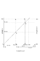
- FIG. 6 is a diagram showing a change in the threshold value when the comparison circuit 21a is used.
- the straight line shown by the dotted line shows the relationship between the input voltage Vin_org input to the logic circuit 50 of FIG. 4 and the applied voltage applied to the gate electrodes of the NMOS transistors 51 and 52 and the MIMO transistors 54 and 55. ing.
- the straight line indicated by the alternate long and short dash line is a straight line indicating the change in voltage VNG with respect to the input voltage Vin input to the comparison circuit 21a. That is, the straight line indicated by the alternate long and short dash line is a straight line indicating the change in the applied voltage applied to the gate electrodes of the NMOS transistors 51 and 52 with respect to the input voltage Vin.
- the straight line shown by the alternate long and short dash line is a straight line showing the change of the voltage VPG with respect to the input voltage Vin input to the comparison circuit 21a. That is, the straight line indicated by the alternate long and short dash line is a straight line indicating the change in the applied voltage applied to the gate electrodes of the MPa transistors 54 and 55 with respect to the input voltage Vin.
- the input voltage Vin changes from a low voltage (for example, 0V) to a high voltage (for example, VDD), and the voltage VNG is the same voltage level as the voltage level indicated by the point A1, the voltage level indicated by the point A2 (for example, VDD). That is, when VtH_org), the logical level of the output voltage Vout changes from the “H” level to the “L” level as shown by the solid line passing through the point A2. Therefore, when the voltage level of the voltage VNG reaches the point A2, the input voltage Vin becomes the high threshold voltage VtH of the comparison circuit 21a.
- the comparison circuit 21a applies the voltages VNG and VPG generated by the voltage conversion circuit 40a to the NMOS transistors 51 and 52 and the MPa transistors 54 and 55.
- the comparison circuit 21a has a high threshold voltage VtH_org and a low threshold voltage VtL_org determined by the threshold value of the MOS transistor, and the comparison circuit 21a has a high threshold voltage VtH and a low threshold voltage VtL. Can be changed to. Therefore, the comparison circuit 21a can change the hysteresis characteristic of the logic circuit 50.
- the value of the high threshold voltage VtH_org depends on the voltage corresponding to the respective threshold voltage vttn of the NMOS transistors 51 and 52.
- the value of the low threshold voltage VtL_org depends on the voltage corresponding to the respective threshold voltage vtp of the epitaxial transistors 54 and 55.
- a low threshold voltage can be used, in which case the hysteresis characteristics can be changed.
- the conventional logic circuit 50 of FIG. 4 is used as the logic circuit 50. It is necessary to use a plurality of differential amplifiers for a hysteresis analyzer that can change the hysteresis width and the threshold value from "H" level to "L” level and from “L” level to “H” level.
- the differential amplifier has a large area, and it is necessary to keep the bias current flowing when operating the differential amplifier, which increases the power consumption.
- the output of the logic circuit 50 is stable at a high level, the NMOS transistors 51 and 52 are off, so that no through current flows through the logic circuit 50.
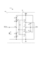
- FIG. 7 is a diagram showing an example of the configuration of the comparison circuit 21b.
- the voltage conversion circuit 40b of the comparison circuit 21b is a voltage conversion circuit 40a of the comparison circuit 21a with a resistor 45 added between the node to which the input voltage is applied and the ground.
- FIG. 8 is a diagram showing an example of the configuration of the comparison circuit 21c.
- the voltage conversion circuit may be realized with a configuration different from that of the voltage conversion circuits 40a and 40b.
- the input voltage Vin is applied to the gate electrode and the source follower circuit 61a for outputting the voltage VNGb from the source electrode, and the input voltage Vin is applied to the gate electrode and the voltage VPGb is applied from the source electrode. It is composed of a source follower circuit 61b that outputs the above.
- the source follower circuit 61a includes a constant current source 62a and a epitaxial transistor 63a. Further, the source follower circuit 61b includes a constant current source 62b and an NMOS transistor 63b.
- the source follower circuit 61a corresponds to the "first source follower circuit”
- the source follower circuit 62b corresponds to the "second source follower circuit”.
- the voltage VNGb which is the output of the source follower circuit 61a, is basically a voltage in which the input voltage Vin is shifted by the gate-source voltage of the epitaxial transistor 63a.
- the voltage VPGb which is the output of the source follower circuit 61b, is in the form of outputting a voltage shifted by the gate-source voltage of the NMOS transistor 63b.
- the input voltage Vin that exceeds the output amplitude after deducting the voltage drop used in the constant current source or transistor is cut and output, so the amplitude of the voltage VNGb or voltage VPGb is a low power supply.
- the voltage is less than the potential difference between VDD and ground voltage.
- the voltage conversion circuit 40c Since the voltage conversion circuit 40c receives the input voltage Vin, a high withstand voltage element is required. However, since the amplitude of the voltage VNG that receives the output of the source follower circuit that operates at the low power supply voltage VDD and the voltage VPG is less than the potential difference between the ground voltage and the low power supply voltage VDD, a high withstand voltage element is used in the comparison circuit 21a. Even if it is not, the destruction of the element can be prevented more reliably. Therefore, in this modification, the voltage conversion circuit 40c uses a high withstand voltage element, and the logic circuit 50 that operates with a potential difference between the low power supply voltage VDD and the ground voltage uses a low withstand voltage element.
- the power module 10 of the present embodiment has been described above.
- the hysteresis characteristic is determined by the threshold voltages of the NMOS transistors 51 and 52 and the epitaxial transistors 54 and 55, and it is difficult to change the hysteresis characteristic.
- the input voltage Vin is converted into a voltage VNG and a voltage VPG, and the input voltage is applied to the gate electrodes of the NMOS transistors 51 and 52 and the gate electrodes of the epitaxial transistors 54 and 55, respectively.
- the hysteresis characteristics seen from Vin can be changed.
- the input voltage Vin is higher than the power supply voltage VDD of the logic circuit 50, and high withstand voltage MOS transistors are used for the NMOS transistors 51 to 53 and the MIMO transistors 54 to 56.
- the logic circuit 50 if the logic circuit 50 is used, the hysteresis characteristic determined by the threshold value of the high withstand voltage MOS transistor can be changed by adjusting the resistance values R1 to R4 of the resistors 41 to 44.
- the logic circuit 50 when the NMOS transistor 32 is turned on by the low-side drive circuit 27, the voltage Vs of the terminal VS may become a negative voltage due to the influence of the inductor component of the load 11. Then, a current may flow from the ground to the voltage line to which the voltage Vs of the terminal VS is applied, and the potential of the terminal G (for example, ground) may fluctuate. As a result, the low power supply voltage VDD may fluctuate.
- the logic circuit 50 By configuring the logic circuit 50 with two PRIVATE transistors and two NMOS transistors, it is affected by the fluctuation of the bias current that occurs when the low power supply voltage VDD fluctuates when a comparator is used as the Schmitt trigger circuit. Absent. Therefore, the logic circuit 50 operates as a highly accurate Schmitt trigger circuit.
- the resistance values R1 to R4 of the resistors 41 to 44 are determined so that either the pair of the two PIXTA transistors 54, 55 or the pair of the NMOS transistors 51, 52 of the logic circuit 50 is turned off. As a result, even if the input voltage Vin is not applied to the node N1, the through current can be prevented from flowing through the logic circuit 50.
- the voltage conversion circuit 40b is realized by two source follower circuits. Thereby, as in the case of the logic circuit 50, the hysteresis characteristic seen from the input voltage Vin can be changed.
- the node N1 when the resistor 45 is connected between the node N1 and the ground, the node N1 can be pulled down when the input voltage Vin is not applied to the node N1, and the resistance values R1 of the resistors 41 to 44 can be pulled down.
- ⁇ R4 can be designed freely to some extent.
Landscapes
- Physics & Mathematics (AREA)
- Engineering & Computer Science (AREA)
- Power Engineering (AREA)
- Nonlinear Science (AREA)
- General Physics & Mathematics (AREA)
- Computer Hardware Design (AREA)
- Computing Systems (AREA)
- General Engineering & Computer Science (AREA)
- Mathematical Physics (AREA)
- Logic Circuits (AREA)
- Manipulation Of Pulses (AREA)
- Measurement Of Current Or Voltage (AREA)
Abstract
Description
この出願は、2019年12月3日に出願された日本特許出願、特願2019-218974に基づく優先権を主張し、その内容を援用する。
<パワーモジュール10>
図1は、本発明の一実施形態であるパワーモジュール10の構成の一例を示す図である。パワーモジュール10は、電力変換用のパワー半導体及び駆動回路を含み、例えば負荷11を駆動する半導体装置である。パワーモジュール10は、ブートストラップ電圧Vbを生成するためのコンデンサ14、HVIC20、ブリッジ回路30、端子PWR,D,P,S,N,COMを含む。
図2は、HVIC20の構成の一例を示す図である。HVIC(High Voltage Integrated Circuit)20は、比較回路21、インバータ22、フィルタ回路23、パルス生成回路24、ハイサイド駆動回路25、電源回路26、ローサイド駆動回路27、端子PVCC,DS,VB,H,VS,L,Gを含む。
==本実施形態の比較回路21a==
図3は、比較回路21の一実施形態である比較回路21aの構成を示す図である。
VPG=(R4/(R3+R4))×Vin・・・(2)
論理回路50は、電圧VNG,VPGの電圧レベルの変化に応じて、出力電圧Voutの論理レベルを、ヒステリシス特性を有して変化させるシュミットトリガ回路である。論理回路50は、NMOSトランジスタ51~53と、PMOSトランジスタ54~56と、を含んで構成される。
ここで、シュミットトリガ回路の基本的な動作を説明するために、論理回路50の、2つのNMOSトランジスタ51,52と、2つのPMOSトランジスタ54,55と、のゲートが共通の図4に示す回路について説明する。なお、ここでは、論理回路50の、2つのNMOSトランジスタ51,52と、2つのPMOSトランジスタ54,55と、のゲートに印可される電圧を、入力電圧Vin_orgとする。
図5は、論理回路50の動作を説明する図である。図5を用いて、論理回路50のNMOSトランジスタ51~53及びPMOSトランジスタ54~56の動作を説明する。
以上の通り、論理回路50は、高いしきい値電圧VtH_orgと,低いしきい値電圧VtL_orgと、によって実現されるヒステリシス特性を有している。高いしきい値電圧VtH_orgは、NMOSトランジスタ51,52が共にオンする条件に基づいて決定される。また、低いしきい値電圧VtL_orgは、PMOSトランジスタ54,55が共にオンする条件に基づいて決定される。
VGS52=Vin_org-Vx・・・(4)
VGS53=Vout-Vx・・・(5)
図5のX1において、入力電圧Vin_orgが0Vであるとき、NMOSトランジスタ51,52はオフされ、NMOSトランジスタ53はオンされる。
ここで、β1及びβ3は、それぞれNMOSトランジスタ51,53の物理構造によって決定される係数である。例えば、β=μCoxW/Lであり、μは、移動度であり、Coxは、ゲート酸化膜の単位面積のキャパシタンスであり、Wは、ゲート幅、Lは、ゲート長である。
入力電圧Vinがより高い電圧となり、高いしきい値電圧VtH_orgとなり、VGS52=Vin_org-Vx=vtnとなると、NMOSトランジスタ52は、オンされる。NMOSトランジスタ51,52がオンされるので、出力電圧Voutは0Vとなる。このときの入力電圧Vin_orgをVtH_orgとすると、以下の式(8)が成立する。
式(8)からVtH_orgを求めると、以下の式(9)が成立する。
なお、NMOSトランジスタ51,52がオンされると、Vx=Vout=0となり、VGS53=0となるので、NMOSトランジスタ53はオフされる。
VGS55=Vin_org-VDD・・・(11)
VGS56=Vout-Vy・・・(12)
入力電圧Vin_orgがVDDであるとき、PMOSトランジスタ54,55はオフされ、PMOSトランジスタ56はオンされる。この時、Vout=0、Vy=vtpである。
ここで、β5及びβ6は、それぞれPMOSトランジスタ55,56の物理構造によって決定される係数である。例えば、β=μCoxW/Lであり、μは、移動度であり、Coxは、ゲート酸化膜の単位面積のキャパシタンスであり、Wは、ゲート幅、Lは、ゲート長である。
入力電圧Vin_orgがより低い電圧となり、VGS54=Vin_org-Vy=vtpとなると、PMOSトランジスタ54は、オンされる。PMOSトランジスタ54,55がオンされるので、出力電圧VoutはVDDとなる。このときの入力電圧Vin_orgをVtL_orgとすると、以下の式(15)が成立する。
式(15)からVtL_orgを求めると、以下の式(16)が成立する。
なお、PMOSトランジスタ54,55がオンされると、Vy=Vout=VDDとなり、VGS56=0となるので、PMOSトランジスタ56はオフされる。
比較回路21aでは、NMOSトランジスタ51,52のゲート電極には、電圧VNGが印可され、PMOSトランジスタ54,55のゲート電極には、電圧VPGが印可されている。
VtH_org=(R1/(R1+R2))×VtH+(R2/(R1+R2))×VDD・・・(17)
式(17)から高いしきい値電圧VtHを求めると、以下の通りとなる。
同様に、論理回路50の低いしきい値電圧VtL_orgが論理回路50に印加されるとき、比較回路21aの制御信号INの電圧レベルが入力電圧Vinとしてしきい値電圧VtLとなる場合、式(2)から
VtL_org=(R4/(R3+R4))×VtL・・・(19)
式(19)から低いしきい値電圧VtLを求めると、以下の通りとなる。
以上から、比較回路21aの高いしきい値電圧VtH及び低いしきい値電圧VtLは、論理回路50の高いしきい値電圧VtH_org及び低いしきい値電圧VtL_orgと異なる値とすることができる。そして、比較回路21aを用いれば、抵抗41~44の抵抗値R1~R4を変更することで、比較回路21aの高いしきい値電圧VtH及び低いしきい値電圧VtLを、変化させることができる。そのため、論理回路50のヒステリシス特性を変化させることができる。
図6は、比較回路21aを用いた場合のしきい値の変化を示す図である。図6において、点線で示された直線は、図4の論理回路50に入力される入力電圧Vin_org及びNMOSトランジスタ51,52、PMOSトランジスタ54,55のゲート電極に印可される印可電圧の関係を示している。
==比較回路21b==
図7は、比較回路21bの構成の一例を示す図である。比較回路21bの電圧変換回路40bは、比較回路21aの電圧変換回路40aに、さらに、入力電圧が印可されるノードと、接地と、の間に抵抗45を加えたものである。
図8は、比較回路21cの構成の一例を示す図である。電圧変換回路は、電圧変換回路40a,40bとは異なる構成で実現されてもよい。一例として、電圧変換回路40cは、入力電圧Vinが、ゲート電極に印可され、ソース電極から電圧VNGbを出力するソースフォロア回路61aと、入力電圧Vinが、ゲート電極に印可され、ソース電極から電圧VPGbを出力するソースフォロア回路61bと、で構成される。
以上、本実施形態のパワーモジュール10について説明した。比較回路21として、シュミットトリガ回路を用いる場合、ヒステリシス特性は、NMOSトランジスタ51,52、PMOSトランジスタ54,55のそれぞれのしきい値電圧によって決められ、ヒステリシス特性を変化させることは難しかった。しかしながら、入力電圧Vinを、電圧VNGと、電圧VPGと、に変換し、それぞれを、NMOSトランジスタ51,52のゲート電極と、PMOSトランジスタ54,55のゲート電極と、に印可することによって、入力電圧Vinから見たヒステリシス特性を変化させることができる。
11 負荷
12,14 コンデンサ
13 直流電源
20 HVIC
21,21a,21b,21c 比較回路
22 インバータ
23 フィルタ回路
24 パルス生成回路
25 ハイサイド駆動回路
26 電源回路
27 ローサイド駆動回路
30 ブリッジ回路
31,32,51~53,63b NMOSトランジスタ
40a,40b,40c 電圧変換回路
41~45 抵抗
50 論理回路
54~56,63a PMOSトランジスタ
61a,61b ソースフォロア回路
62a,62b 定電流源
Claims (8)
- 入力電圧が、第1しきい値電圧を上回ると、第1論理レベルの出力電圧を出力し、前記入力電圧が、前記第1しきい値電圧より低い第2しきい値電圧を下回ると、第2論理レベルの前記出力電圧を出力する、比較回路であって、
前記入力電圧を、第1電圧と、前記第1電圧より低い第2電圧と、に変換する変換回路と、
前記第1電圧が、第3しきい値電圧を上回ると、前記第1論理レベルの前記出力電圧を出力し、前記第2電圧が、前記第3しきい値電圧より低い第4しきい値電圧を下回ると、前記第2論理レベルの前記出力電圧を出力する論理回路と、
を備える、比較回路。 - 請求項1に記載の比較回路であって、
前記論理回路は、前記入力電圧の最大値より低い電源電圧で動作する、比較回路。 - 請求項1または2に記載の比較回路であって、
前記論理回路は、
2つのゲート電極のそれぞれに前記第2電圧が印可され、直列に接続された、電源側の2つのPMOSトランジスタと、
2つのゲート電極のそれぞれに前記第1電圧が印可され、前記2つのPMOSトランジスタと、接地と、の間に直列に接続された2つのNMOSトランジスタと、
を備えたシュミットトリガ回路であり、
前記第3しきい値電圧は、前記2つのNMOSトランジスタのそれぞれのしきい値電圧に応じた電圧であり、前記第4しきい値電圧は、前記2つのPMOSトランジスタのそれぞれのしきい値電圧に応じた電圧である、比較回路。 - 請求項3に記載の比較回路であって、
前記変換回路は、
前記論理回路の電源電圧が印可されるノードと、接地と、の間に直列に接続された第1抵抗から第4抵抗を備え、
前記変換回路は、
前記第2抵抗及び前記第3抵抗の接続点に前記入力電圧が印可されると、前記第1抵抗及び前記第2抵抗の接続点において前記第1電圧を生成し、前記第3抵抗及び前記第4抵抗の接続点において前記第2電圧を生成する、比較回路。 - 請求項4に記載の比較回路であって、
前記第1抵抗から前記第4抵抗は、前記変換回路に前記入力電圧が印可されない場合、前記2つのPMOSトランジスタの組または前記2つのNMOSトランジスタの組のうちの何れかの組をオフする抵抗値を有する、比較回路。 - 請求項1~3のうちの何れか一項に記載の比較回路であって、
前記変換回路は、
前記入力電圧が、ゲート電極に印可され、ソース電極から前記第1電圧を出力する第1ソースフォロア回路と、
前記入力電圧が、ゲート電極に印可され、ソース電極から前記第2電圧を出力する第2ソースフォロア回路と、
を備える、比較回路。 - 請求項1~6のうちの何れか一項に記載の比較回路であって、
前記変換回路は、
前記入力電圧が印可されるノードと、接地と、の間に接続された抵抗をさらに備える、比較回路。 - 電源電圧から、前記電源電圧より低い低電源電圧を生成する電源回路と、前記低電源電圧で動作し、上側アームのスイッチング素子及び下側アームのスイッチング素子を駆動するための制御信号を検出する検出回路と、前記検出回路の検出結果に基づいて、前記上側アームのスイッチング素子及び前記下側アームのスイッチング素子を駆動する駆動回路と、を備えた半導体装置であって、
前記検出回路は、
前記制御信号の電圧レベルが第1しきい値電圧を上回ると、第1論理レベルの前記検出結果を出力し、前記制御信号の電圧レベルが前記第1しきい値電圧より低い第2しきい値電圧を下回ると、第2論理レベルの前記検出結果を出力する比較回路を備え、
前記比較回路は、
前記制御信号の電圧レベルを、第1電圧と、前記第1電圧より低い第2電圧と、に変換する変換回路と、
前記第1電圧が第3しきい値電圧を上回ると、前記第1論理レベルの前記検出結果を出力し、前記第2電圧が前記第3しきい値電圧より低い第4しきい値電圧を下回ると、前記第2論理レベルの前記検出結果を出力する論理回路と、
を備える、半導体装置。
Priority Applications (4)
| Application Number | Priority Date | Filing Date | Title |
|---|---|---|---|
| DE112020002135.1T DE112020002135T5 (de) | 2019-12-03 | 2020-10-28 | Komparatorschaltung und halbleitervorrichtung |
| CN202080039929.9A CN113875155B (zh) | 2019-12-03 | 2020-10-28 | 比较电路、半导体装置 |
| JP2021562500A JP7416087B2 (ja) | 2019-12-03 | 2020-10-28 | 比較回路、半導体装置 |
| US17/535,336 US11784636B2 (en) | 2019-12-03 | 2021-11-24 | Comparator circuit and semiconductor device |
Applications Claiming Priority (2)
| Application Number | Priority Date | Filing Date | Title |
|---|---|---|---|
| JP2019-218974 | 2019-12-03 | ||
| JP2019218974 | 2019-12-03 |
Related Child Applications (1)
| Application Number | Title | Priority Date | Filing Date |
|---|---|---|---|
| US17/535,336 Continuation US11784636B2 (en) | 2019-12-03 | 2021-11-24 | Comparator circuit and semiconductor device |
Publications (1)
| Publication Number | Publication Date |
|---|---|
| WO2021111772A1 true WO2021111772A1 (ja) | 2021-06-10 |
Family
ID=76221183
Family Applications (1)
| Application Number | Title | Priority Date | Filing Date |
|---|---|---|---|
| PCT/JP2020/040385 Ceased WO2021111772A1 (ja) | 2019-12-03 | 2020-10-28 | 比較回路、半導体装置 |
Country Status (5)
| Country | Link |
|---|---|
| US (1) | US11784636B2 (ja) |
| JP (1) | JP7416087B2 (ja) |
| CN (1) | CN113875155B (ja) |
| DE (1) | DE112020002135T5 (ja) |
| WO (1) | WO2021111772A1 (ja) |
Families Citing this family (4)
| Publication number | Priority date | Publication date | Assignee | Title |
|---|---|---|---|---|
| US11569808B2 (en) * | 2020-11-02 | 2023-01-31 | Texas Instruments Incorporated | Wide high voltage swing input comparator stage with matching overdrive |
| US11418187B1 (en) * | 2021-09-27 | 2022-08-16 | Advanced Micro Devices, Inc. | Low voltage power on reset circuit |
| CN114499474A (zh) * | 2022-04-14 | 2022-05-13 | 广东省大湾区集成电路与系统应用研究院 | 低边驱动电路、芯片及电子设备 |
| CN115296530A (zh) * | 2022-07-25 | 2022-11-04 | 圣邦微电子(北京)股份有限公司 | 一种电源管理芯片 |
Citations (3)
| Publication number | Priority date | Publication date | Assignee | Title |
|---|---|---|---|---|
| US5945859A (en) * | 1997-04-24 | 1999-08-31 | Lg Semicon Co., Ltd. | Trigger voltage controllable Schmitt trigger circuit |
| JP2002300011A (ja) * | 2001-03-30 | 2002-10-11 | Seiko Instruments Inc | ヒステリシス付き電圧比較器 |
| US20200082392A1 (en) * | 2018-09-11 | 2020-03-12 | Shervin Pishevar | Geolocation-based payment platforms for ride-sharing transportation |
Family Cites Families (61)
| Publication number | Priority date | Publication date | Assignee | Title |
|---|---|---|---|---|
| US3984703A (en) * | 1975-06-02 | 1976-10-05 | National Semiconductor Corporation | CMOS Schmitt trigger |
| US4464587A (en) * | 1980-10-14 | 1984-08-07 | Tokyo Shibaura Denki Kabushiki Kaisha | Complementary IGFET Schmitt trigger logic circuit having a variable bias voltage logic gate section |
| JPS5923915A (ja) * | 1982-07-30 | 1984-02-07 | Toshiba Corp | シユミツトトリガ回路 |
| US5194767A (en) * | 1990-12-19 | 1993-03-16 | Texas Instruments Incorporated | TTL compatible hysteresis input buffer with improvable AC margin |
| US5602496A (en) * | 1992-06-17 | 1997-02-11 | Advanced Micro Devices, Inc. | Input buffer circuit including an input level translator with sleep function |
| JPH0653783A (ja) | 1992-07-31 | 1994-02-25 | Kawasaki Steel Corp | シュミットトリガ回路 |
| US5336942A (en) * | 1992-08-12 | 1994-08-09 | Western Digital (Singapore) Pty, Ltd. | High speed Schmitt trigger with process, temperature and power supply independence |
| US5319323A (en) * | 1992-08-19 | 1994-06-07 | Hyundai Electronics America | Power supply compensated MOS Schmitt trigger oscillator |
| US5341033A (en) * | 1992-11-23 | 1994-08-23 | Analog Devices, Inc. | Input buffer circuit with deglitch method and apparatus |
| FR2719135B1 (fr) * | 1994-04-21 | 1996-06-28 | Sgs Thomson Microelectronics | Circuit de limitation de tension avec comparateur à hystérésis. |
| US6356099B1 (en) * | 1994-11-10 | 2002-03-12 | Advanced Micro Devices, Inc. | Transmission-line-noise immune input buffer |
| US6181172B1 (en) * | 1995-12-27 | 2001-01-30 | Philips Electronics North America Corp. | High voltage detect circuit with increased long term reliability |
| FR2758422B1 (fr) * | 1997-01-13 | 1999-02-05 | Sgs Thomson Microelectronics | Oscillateur en anneau en technologie cmos |
| JP3623624B2 (ja) | 1997-01-16 | 2005-02-23 | 日本電気エンジニアリング株式会社 | ヒステリシスコンパレータ |
| KR100215839B1 (ko) * | 1997-03-20 | 1999-08-16 | 구본준 | 트리거 전압 조정이 가능한 슈미트 트리거 회로 |
| JPH11142477A (ja) * | 1997-11-06 | 1999-05-28 | Fujitsu Ltd | 半導体集積回路 |
| US6124733A (en) * | 1997-12-22 | 2000-09-26 | Advanced Micro Devices, Inc. | Input buffer providing virtual hysteresis |
| US6046617A (en) * | 1998-06-25 | 2000-04-04 | National Semiconductor Corporation | CMOS level detection circuit with hysteresis having disable/enable function and method |
| US6060925A (en) * | 1998-08-06 | 2000-05-09 | Taiwan Semiconductor Manufacturing Co., Ltd. | Schmitt-trigger circuit with low power consumption |
| FR2812984B1 (fr) * | 2000-08-11 | 2002-10-11 | St Microelectronics Sa | Amplificateur a seuil |
| US6433602B1 (en) * | 2000-08-30 | 2002-08-13 | Lattice Semiconductor Corp. | High speed Schmitt Trigger with low supply voltage |
| US6441663B1 (en) * | 2000-11-02 | 2002-08-27 | International Business Machines Corporation | SOI CMOS Schmitt trigger circuits with controllable hysteresis |
| CA2325685A1 (en) * | 2000-11-10 | 2002-05-10 | Ibm Canada Limited-Ibm Canada Limitee | Multiple-channel optical transceiver input buffer with zero static current and symmetrical hysteresis |
| WO2002103907A1 (en) * | 2001-06-20 | 2002-12-27 | Koninklijke Philips Electronics N.V. | Input pad with improved noise immunity and output characteristics |
| US6448830B1 (en) * | 2001-11-05 | 2002-09-10 | International Business Machines Corporation | Single-stage tri-state Schmitt trigger |
| US6870413B1 (en) * | 2001-12-14 | 2005-03-22 | Altera Corporation | Schmitt trigger circuit with adjustable trip point voltages |
| US6624678B1 (en) * | 2002-10-09 | 2003-09-23 | Analog Devices, Inc. | Schmitt trigger device with disable |
| JP2005191821A (ja) * | 2003-12-25 | 2005-07-14 | Seiko Epson Corp | コンパレータ回路及び電源回路 |
| US7183826B2 (en) * | 2004-03-11 | 2007-02-27 | Seiko Epson Corporation | High hysteresis width input circuit |
| US7167032B1 (en) * | 2004-03-31 | 2007-01-23 | Lattice Semiconductor Corporation | Self-adjusting Schmitt trigger |
| KR100559406B1 (ko) * | 2004-10-15 | 2006-03-10 | 삼성전자주식회사 | 히스테리시스를 갖는 비교기 및 그것을 사용한 비교 방법 |
| EP1662660A3 (en) * | 2004-11-29 | 2007-12-12 | STMicroelectronics Pvt. Ltd | Method and apparatus for providing compensation against temperature, process and supply voltage variation |
| JP4471226B2 (ja) * | 2007-07-23 | 2010-06-02 | 統寶光電股▲ふん▼有限公司 | 半導体集積回路 |
| TWI345377B (en) * | 2008-01-28 | 2011-07-11 | Faraday Tech Corp | Schmitt trigger as level detection circuit |
| US8115531B1 (en) * | 2008-03-31 | 2012-02-14 | Lsi Corporation | D flip-flop having enhanced immunity to single-event upsets and method of operation thereof |
| CN101777905B (zh) * | 2009-01-12 | 2012-04-25 | 辉芒微电子(深圳)有限公司 | 一种逻辑电平转换电路 |
| JP2012238986A (ja) | 2011-05-11 | 2012-12-06 | Toshiba Corp | シュミットトリガ回路 |
| FR2977749A1 (fr) * | 2011-07-04 | 2013-01-11 | St Microelectronics Crolles 2 | Cellule elementaire d'un circuit integre peu sensible aux perturbations exterieures |
| US8723584B2 (en) * | 2012-05-03 | 2014-05-13 | Conexant Systems, Inc. | Low power dual voltage mode receiver |
| CN103066955B (zh) * | 2012-12-17 | 2016-01-20 | 广州慧智微电子有限公司 | 一种用于绝缘硅工艺的小尺寸、快速翻转施密特触发器电路 |
| US8736333B1 (en) * | 2013-01-08 | 2014-05-27 | Freescale Semiconductor, Inc. | Schmitt trigger circuit with near rail-to-rail hysteresis |
| US8829964B1 (en) * | 2013-03-15 | 2014-09-09 | Freescale Semiconductor, Inc. | Compensated hysteresis circuit |
| US9306550B2 (en) * | 2014-03-17 | 2016-04-05 | Stmicroelectronics International N.V. | Schmitt trigger in FDSOI technology |
| JP6398411B2 (ja) * | 2014-07-17 | 2018-10-03 | 富士電機株式会社 | 半導体装置および電力変換装置 |
| KR102242582B1 (ko) * | 2014-10-10 | 2021-04-22 | 삼성전자주식회사 | 수신 회로 및 그것의 신호 수신 방법 |
| CN107408939B (zh) * | 2015-04-01 | 2020-09-25 | 国立研究开发法人科学技术振兴机构 | 电子电路 |
| CN106505990B (zh) * | 2015-09-08 | 2021-12-03 | 恩智浦美国有限公司 | 具有可选滞后和速度的输入缓冲器 |
| JP2017079431A (ja) * | 2015-10-21 | 2017-04-27 | 株式会社東芝 | 電圧比較回路 |
| DE112017000186B4 (de) | 2016-02-16 | 2022-05-05 | Fuji Electric Co., Ltd. | Halbleitervorrichtung |
| JP2017169153A (ja) | 2016-03-18 | 2017-09-21 | 株式会社リコー | 半導体回路装置 |
| US10141045B2 (en) * | 2016-12-15 | 2018-11-27 | Taiwan Semiconductor Manufacturing Co., Ltd. | Dual rail device with power detector for controlling power to first and second power domains |
| US10483973B2 (en) * | 2017-12-06 | 2019-11-19 | Taiwan Semiconductor Manufacturing Co., Ltd. | Temperature instability-aware circuit |
| CN108649939B (zh) * | 2018-04-16 | 2022-07-29 | 芯原微电子(上海)股份有限公司 | 电源检测电路及方法 |
| JP2019218974A (ja) | 2018-06-18 | 2019-12-26 | アイシン精機株式会社 | クラッチ制御装置 |
| US10622979B2 (en) * | 2018-08-20 | 2020-04-14 | Texas Instruments Incorporated | Delay cell |
| US11171634B2 (en) * | 2019-07-08 | 2021-11-09 | Taiwan Semiconductor Manufacturing Co. Ltd. | Buffer circuit between different voltage domains |
| JP7505267B2 (ja) * | 2019-11-15 | 2024-06-25 | 富士電機株式会社 | スイッチング制御回路、半導体装置 |
| US11296683B2 (en) * | 2020-03-24 | 2022-04-05 | SiFive, Inc. | Low-swing Schmitt triggers |
| US11223345B2 (en) * | 2020-06-04 | 2022-01-11 | Stmicroelectronics International N.V. | Low power input receiver using a Schmitt trigger circuit |
| US11146253B1 (en) * | 2020-08-24 | 2021-10-12 | Electronics And Telecommunications Research Institute | Receiving circuit to process low-voltage signal with hysteresis |
| US11444611B2 (en) * | 2020-10-06 | 2022-09-13 | Mediatek Inc. | Chip having a receiver including a hysteresis circuit |
-
2020
- 2020-10-28 WO PCT/JP2020/040385 patent/WO2021111772A1/ja not_active Ceased
- 2020-10-28 CN CN202080039929.9A patent/CN113875155B/zh active Active
- 2020-10-28 DE DE112020002135.1T patent/DE112020002135T5/de active Pending
- 2020-10-28 JP JP2021562500A patent/JP7416087B2/ja active Active
-
2021
- 2021-11-24 US US17/535,336 patent/US11784636B2/en active Active
Patent Citations (3)
| Publication number | Priority date | Publication date | Assignee | Title |
|---|---|---|---|---|
| US5945859A (en) * | 1997-04-24 | 1999-08-31 | Lg Semicon Co., Ltd. | Trigger voltage controllable Schmitt trigger circuit |
| JP2002300011A (ja) * | 2001-03-30 | 2002-10-11 | Seiko Instruments Inc | ヒステリシス付き電圧比較器 |
| US20200082392A1 (en) * | 2018-09-11 | 2020-03-12 | Shervin Pishevar | Geolocation-based payment platforms for ride-sharing transportation |
Also Published As
| Publication number | Publication date |
|---|---|
| JPWO2021111772A1 (ja) | 2021-06-10 |
| CN113875155B (zh) | 2025-08-29 |
| US11784636B2 (en) | 2023-10-10 |
| CN113875155A (zh) | 2021-12-31 |
| JP7416087B2 (ja) | 2024-01-17 |
| DE112020002135T5 (de) | 2022-01-13 |
| US20220085798A1 (en) | 2022-03-17 |
Similar Documents
| Publication | Publication Date | Title |
|---|---|---|
| US11876510B2 (en) | Load driver | |
| JP7416087B2 (ja) | 比較回路、半導体装置 | |
| US7952400B2 (en) | Reset device | |
| US20090189665A1 (en) | Schmitt-trigger-based level detection circuit | |
| US8884653B2 (en) | Comparator and ad converter provided therewith | |
| CN101989842A (zh) | 运算放大器和使用运算放大器的半导体器件 | |
| CN102195637A (zh) | 传输门电路及半导体装置 | |
| JP6672063B2 (ja) | Dcdcコンバータ | |
| CN107168433B (zh) | 输出电路 | |
| JP2013141113A (ja) | 電圧比較回路 | |
| CN111693759A (zh) | 电压检测器 | |
| WO2018055666A9 (ja) | インターフェース回路 | |
| US20130120046A1 (en) | Analog rail-to-rail comparator with hysteresis | |
| US10812059B2 (en) | Comparator | |
| JP7097749B2 (ja) | レベルシフト回路 | |
| JP4336315B2 (ja) | 駆動回路 | |
| JP4796437B2 (ja) | 発振回路 | |
| JP3996070B2 (ja) | レベルシフタ回路 | |
| JP2010231498A (ja) | 定電圧電源 | |
| JP4400666B2 (ja) | 半導体集積回路装置およびスイッチ入力回路 | |
| JP2006025085A (ja) | Cmos駆動回路 | |
| JP2021082861A (ja) | コンパレータ | |
| JP6717715B2 (ja) | レギュレータ回路およびセンサ回路 | |
| JP2006203762A (ja) | フリップフロップ回路および半導体装置 | |
| JP3510228B2 (ja) | 電圧比較回路 |
Legal Events
| Date | Code | Title | Description |
|---|---|---|---|
| 121 | Ep: the epo has been informed by wipo that ep was designated in this application |
Ref document number: 20895731 Country of ref document: EP Kind code of ref document: A1 |
|
| ENP | Entry into the national phase |
Ref document number: 2021562500 Country of ref document: JP Kind code of ref document: A |
|
| 122 | Ep: pct application non-entry in european phase |
Ref document number: 20895731 Country of ref document: EP Kind code of ref document: A1 |
|
| WWG | Wipo information: grant in national office |
Ref document number: 202080039929.9 Country of ref document: CN |