WO2021095164A1 - Dispositif optique - Google Patents
Dispositif optique Download PDFInfo
- Publication number
- WO2021095164A1 WO2021095164A1 PCT/JP2019/044532 JP2019044532W WO2021095164A1 WO 2021095164 A1 WO2021095164 A1 WO 2021095164A1 JP 2019044532 W JP2019044532 W JP 2019044532W WO 2021095164 A1 WO2021095164 A1 WO 2021095164A1
- Authority
- WO
- WIPO (PCT)
- Prior art keywords
- lens
- optical
- optical waveguide
- end surface
- light
- Prior art date
Links
Images


Classifications
-
- G—PHYSICS
- G02—OPTICS
- G02B—OPTICAL ELEMENTS, SYSTEMS OR APPARATUS
- G02B6/00—Light guides; Structural details of arrangements comprising light guides and other optical elements, e.g. couplings
- G02B6/24—Coupling light guides
- G02B6/26—Optical coupling means
- G02B6/32—Optical coupling means having lens focusing means positioned between opposed fibre ends
-
- G—PHYSICS
- G02—OPTICS
- G02B—OPTICAL ELEMENTS, SYSTEMS OR APPARATUS
- G02B6/00—Light guides; Structural details of arrangements comprising light guides and other optical elements, e.g. couplings
- G02B6/24—Coupling light guides
- G02B6/26—Optical coupling means
- G02B6/30—Optical coupling means for use between fibre and thin-film device
Definitions
- the present invention relates to an optical device, and more particularly to an optical device that converts the mode field diameter of light to connect between two optical waveguides.
- the mode field diameter of light in each optical waveguide is significantly different. Therefore, in the optical connection between them, a structure for converting the mode field diameter of light, such as a tapered structure or a grating structure, is used.
- the efficiency of optical connection may deteriorate due to variations in the fabrication of the structure that converts the mode field diameter.
- a technique is used in which a lens optical system is configured and the coupling efficiency is compensated within the range of the optical path length constraint.
- An optical system using a single lens has a simple centering process and is used from the viewpoint of cost reduction.
- it is not easy to add various functions such as a problem of return light and wavelength selection.
- an optical system with two lenses it is possible to obtain functions such as suppression of return light and wavelength selection.
- a collimating system using two lenses is constructed between the optical waveguides to be optically connected, and an isolator and a filter are arranged between them.
- the alignment process is increased as compared with the single lens system, and the manufacturing cost is increased. Therefore, as shown in FIG. 17, a structure has been proposed in which the optical waveguide 303 by the clad 301 and the core 302 and the lens 304 are integrated to reduce the alignment process between the lens and the optical waveguide (patented). Reference 1).
- the present invention has been made to solve the above problems, and an object of the present invention is to suppress a decrease in coupling efficiency in an optical system using a plurality of lenses.
- the optical device has a first end surface in which the light of one first optical waveguide to be connected enters and exits, and a first end surface facing the first end surface in which the light of the other second optical waveguide to be connected enters and exits. It is placed between the first lens and the second end face, which is placed between the two end faces and expands the diameter of the mode field of the light emitted from the first end face by waveguideing through the first optical waveguide.
- the second lens that collects the light that has passed through the first lens and the first lens are placed on the plane perpendicular to the optical axis of the first optical waveguide, and the optical axis and the first optical waveguide of the first optical waveguide.
- An adjustment table for adjusting the distance from the main point of one lens and a support portion for supporting the second lens on the side of the second end surface of the second optical waveguide are provided.
- the first lens is mounted, and the optical axis of the first optical waveguide and the principal point of the first lens are formed on a plane perpendicular to the optical axis of the first optical waveguide. Since the adjustment table for adjusting the distance is provided, it is possible to suppress a decrease in coupling efficiency in an optical system using a plurality of lenses.
- FIG. 1 is a cross-sectional view showing a configuration of an optical device according to a first embodiment of the present invention.
- FIG. 2 is a cross-sectional view showing the configuration of the optical device according to the first embodiment of the present invention.
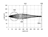
- FIG. 3 is a characteristic diagram showing a calculation result of an optical path when the principal point of the lens of the optical device according to the first embodiment is located on the optical axis of the optical waveguide.
- the y-coordinate (vertical axis) of the intersection (point image position) of the light ray and the image plane is the sine (sin ( ⁇ s)) of the angle ⁇ s formed by the emitted light ray on the light source side and the optical axis 131 and the first optical waveguide.
- FIG. 5 is a characteristic diagram showing the results of plotting with the vertical axis representing NSR and the horizontal axis representing NSS.
- FIG. 9 is a characteristic diagram showing the result of plotting the point image position (y direction) corrected by the position adjustment of the first lens 103 with respect to the NSS.
- FIG. 10 is a characteristic diagram showing the relationship between NSS and NSR before and after the position adjustment of the first lens 103.
- FIG. 11 is a cross-sectional view showing the configuration of the optical device according to the second embodiment of the present invention.
- FIG. 13 is a characteristic diagram showing the relationship between the NSS and the point image position (y direction) after the position adjustment by the first lens 103.
- FIG. 14 is a characteristic diagram showing the relationship between NSS and NSR after the position adjustment by the first lens 103.
- FIG. 15 shows the absolute value of the shift amount (dy1) at the principal point 132 of the first lens 103, the shift amount (dy2) of the principal point 134 of the second lens 104, and the shape of the refracting surface (convex surface) of the second lens 104. It is a characteristic diagram which shows the difference of the point image position by.
- FIG. 16 is a cross-sectional view showing the configuration of another optical device according to the first embodiment of the present invention.
- FIG. 17 is a configuration diagram showing a configuration of an optical device in which the optical waveguide 303 and the lens 304 are integrated.
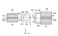
- This optical device optically connects (couples) a first optical waveguide 101 having a first end surface 101a through which light enters and exits and a second optical waveguide 102 having a second end surface 102a through which light enters and exits. It is a device to make it.
- the second end surface 102a is arranged so as to face the first end surface 101a.
- the first optical waveguide 101 and the second optical waveguide 102 are arranged so that the optical axis 131 of the first optical waveguide 101 and the optical axis 133 of the second optical waveguide 102 substantially coincide with each other. ..
- the first optical waveguide 101 is, for example, a so-called silicon optical waveguide composed of a core 101b made of Si and a clad 101c made of silicon oxide.
- the second optical waveguide 102 is a so-called optical fiber composed of a quartz-based core 102b and a clad 102c.
- This optical device includes a first lens 103, a second lens 104, and an adjustment table 105.
- the first lens 103 is arranged between the first end surface 101a and the second end surface 102a, and increases the diameter of the mode field of light emitted from the first end surface 101a by waveguideing through the first optical waveguide 101.
- the first lens 103 is, for example, a spherical (spherically symmetrical) ball lens.
- the first lens 103 is made of, for example, a quartz-based material.
- the second lens 104 is arranged between the first lens 103 and the second end surface 102a, and collects the light that has passed through the first lens 103.
- the second lens 104 is the light that has passed through the first lens 103 in order to connect the light emitted from the first end surface 101a through the first optical waveguide 101 to the second optical waveguide 102 at the second end surface 102a.
- the second lens 104 is, for example, a convex lens having a refracting surface (for example, an ellipsoidal surface) convex toward the first end surface 101a.
- the second optical waveguide 102 is placed (fixed) on the mounting table 111.
- the mounting table 111 is made of, for example, glass.
- the second lens 104 is supported and fixed to the side of the second end surface 102a of the second optical waveguide 102 by the support portion 106.
- the support portion 106 is made of, for example, a resin such as plastic.
- the second lens 104 is formed on a plate-shaped or sheet-shaped support plate 112, and is fixed to the support portion 106 via the support plate 112.
- the support plate 112 can be made of the same resin as the support portion 106.
- the adjustment table 105 places (fixes) the first lens 103 on it. Further, the adjusting table 105 adjusts the distance between the optical axis 131 of the first optical waveguide 101 and the principal point 132 of the first lens 103 on a plane perpendicular to the optical axis 131 of the first optical waveguide 101.
- the adjusting table 105 is made of, for example, the same quartz-based material as the first lens 103.
- the adjusting table 105 is fixed by the adhesive layer 109 on the base 108 on which the mounting table 107 on which the first optical waveguide 101 is placed is fixed.
- the mounting table 107 can be made of, for example, Si.
- the stop member 110 limits the movement of the adjusting table 105 in the optical axis direction.
- the decrease in coupling efficiency in the optical system due to the displacement of the second lens 104 fixedly arranged with respect to the second optical waveguide 102 can be suppressed by adjusting the position of the first lens 103 using the adjusting table 105. To do so.
- the distance between the optical axis 131 of the first optical waveguide 101 and the principal point 132 of the first lens 103 is d1
- the distance between the optical axis 133 of the second optical waveguide 102 and the principal point 134 of the second lens 104 is d2.
- the x-coordinate component of the distance d1 is dx1
- the y-coordinate component is dy1.
- the x-coordinate component of the distance d2 is dx2, and the y-coordinate component is dy2.
- FIG. 3 shows the calculation result of the optical path when the principal point of the lens is located on the optical axis of the optical waveguide. More specifically, the optical axis 131 of the core 101b of the first optical waveguide 101 and the optical axis 133 of the core 102b of the second optical waveguide 102 are coaxial, and the principal points 132 and the second of the first lens 103 This is the case where the principal point 134 of the lens 104 is located on the optical axis described above.
- the first optical waveguide 101 has a reverse taper structure in which the cross-sectional area of the core 101b decreases in the propagation (waveguide) direction, and the numerical aperture of the emitted light is about 0.3 or less.
- the mode field diameter of the waveguide light has been converted. If the numerical aperture does not exceed 0.3, the tapered structure may not be formed.
- the optical path was calculated by the ray tracing method with a numerical aperture of about 0.4 (corresponding to a full-width radiation of 50 degrees).
- the incident end face of the second optical waveguide 102 is defined as an image plane.
- the diameter of the core 102b of the second optical waveguide 102 is 10 ⁇ m.
- the y-coordinate (vertical axis) of the intersection (point image position) of the light ray and the image plane is the sine (sin ( ⁇ s)) of the angle ⁇ s formed by the emitted light ray on the light source side and the optical axis 131 and the first optical waveguide.
- NSS n1 ⁇ sin ( ⁇ s)
- the principal point of the lens is located on the optical axis of the optical waveguide, the emitted light having an NSS of about ⁇ 0.35 to 0.35 is incident on the plane of the core 102b of the second optical waveguide 102. You can see that it does.
- the product NSR (n2 ⁇ sin ( ⁇ r)) of the refractive index n2 between the second optical waveguide 102 and the second lens 104 must satisfy a value determined by the structure of the second optical waveguide 102.
- the ⁇ r corresponding to the maximum value of the NSR that can propagate through the second optical waveguide 102 is called the maximum light receiving angle ⁇ max.
- FIG. 5 shows the results of plotting with NSR on the vertical axis and NSS on the horizontal axis.
- the numerical aperture corresponding to ⁇ max is about 0.1.
- the absolute value of NSR is within 0.1 when it is incident on the second end surface 102a, so that the second optical waveguide 101 is second. It shows that it can propagate through the optical waveguide 102.
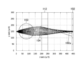
- the optical axis 131 of the core 101b of the first optical waveguide 101, the optical axis 133 of the core 102b of the second optical waveguide 102, and the principal point 132 of the first lens 103 are coaxial with each other, and the principal of the second lens 104 is The case where the point 134 deviates from the optical axis 133 will be described.
- the coupling efficiency of (shifting 134) is shown.
- the point image position shifts downward as a whole, so that the coupling efficiency deteriorates.
- the point image position (y direction) corrected by the position adjustment of the first lens 103 is plotted against the NSS.
- the dotted line ID0 corresponds to the case where the point image position is totally displaced due to the deviation of the principal point of the second lens 104.
- the solid line ID1 when the point image position is corrected by adjusting the position of the first lens 103, it can be seen that the light is focused toward the inside of the core 102b of the second optical waveguide 102.
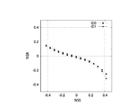
- FIG. 10 shows the relationship between NSS and NSR before and after the position adjustment of the first lens 103.
- the dotted line ID0 indicates before adjustment, and the solid line ID1 indicates after adjustment.
- the NSS can propagate in the second optical waveguide 102 having a numerical aperture of about ⁇ 0.3 to 0.25.
- the structure of the first lens 103 is rotationally symmetric with respect to the axis passing through the principal point 132 parallel to the z-axis, and as shown in FIG. 2, the deviation of the second lens 104 is in the x direction.
- the point image position can be corrected by adjusting the position of the first lens 103 on the same principle.
- This optical device further includes a transparent resin layer 113 arranged so as to fill the space between the second lens 104 and the second end surface 102a in the optical device according to the first embodiment described above.
- the space between the support plate 112 and the second end surface 102a inside the support portion 106 is filled with the transparent resin layer 113.
- the refractive index of the transparent resin layer 113 can be equal to or lower than the refractive index of the second lens 104 and the support plate 112. Further, it is desirable that the coefficient of thermal expansion of the transparent resin layer 113 is about the same as that of the support portion 106 and the support plate 112.
- the optical path length between the second lens 104 and the incident end face of the second optical waveguide 102 is made longer in order to concentrate on the core 102b than when the transparent resin layer 113 is not provided.
- FIG. 13 shows the relationship between the NSS and the point image position (y direction) after the position adjustment by the first lens 103.
- FIG. 14 shows the relationship between NSS and NSR after the position adjustment by the first lens 103. The effect of correcting the point image position by adjusting the position using the first lens 103 can be obtained in the same manner as when the transparent resin layer 113 is not provided.
- FIG. 15 shows the absolute value of the shift amount (dy1) at the principal point 132 of the first lens 103, the shift amount (dy2) of the principal point 134 of the second lens 104, and the shape of the refracting surface (convex surface) of the second lens 104.
- the horizontal axis is NSS and the vertical axis is the point image position.
- the refracting surface of the first lens 103 and the refracting surface of the second lens 104 are spherical surfaces having the same radius of curvature. It is assumed that the light beam after passing through the first lens 103 is converted into collimated light.
- the deviation correction effect of the point image position is that the absolute value of the shift amount dy1 of the first lens 103 is the shift amount dy2 of the second lens 104 between spherical lenses having the same radius of curvature. The smaller it is, the more you get. However, unfocused light rays partially remain in the core 102b (-5 ⁇ m ⁇ y ⁇ 5 ⁇ m).
- the setting of the position of the adjustment table 105 will be described below.
- the profiles of the shift amounts dx2 and dy2 of the principal point 134 of the second lens 104 are acquired in advance.
- the position of the principal point 132 of the first lens 103 is calculated by optical path calculation.
- the position of the adjusting table 105 in the y direction is adjusted by controlling the thickness of the adhesive layer 109.
- the position adjustment of the adjustment table 105 in the x direction is performed by moving the adjustment table 105 in the x direction so that the x coordinate of the principal point 132 of the first lens 103 matches the calculated position.
- the stop member 110 fixed on the base 108 prevents the adjusting table 105 from moving in the optical axis direction.
- the adjusting table 105 is directly placed (arranged) on the base 108 without using the adhesive layer, as shown in FIG. Further, the adjusting table 105 is fixed by the adhesive portion 109a arranged so as to cover the side wall of the adjusting table 105. In this case, the position adjustment of the adjustment table 105 in the y direction is performed by preparing a plurality of adjustment tables 105 having different heights and selecting the adjustment table 105 whose principal point position of the first lens 103 is closest to the calculation position. Do.
- the first optical waveguide may be an optical waveguide composed of a compound semiconductor such as indium phosphide (InP), gallium nitride (GaN), and gallium arsenide (GaAs).
- the second optical waveguide is not limited to the optical fiber, and may be a plane light wave circuit. The same applies to the first optical waveguide.
- the first lens is not limited to a ball lens but can be an aspherical lens.
- the second lens is not limited to an ellipsoidal lens, and may be another aspherical lens or a spherical lens such as a paraboloid or a hyperboloid.
- the optical axis of the first optical waveguide and the principal point of the first lens are mounted on the plane perpendicular to the optical axis of the first optical waveguide. Since an adjustment table for adjusting the distance between the lens and the optical waveguide is provided, the coupling efficiency is reduced due to the fact that the principal point of the lens and the optical axis of the core of the optical waveguide do not match in integrally forming the lens and the optical waveguide. It can be corrected, and a decrease in coupling efficiency in an optical system using a plurality of lenses can be suppressed.
Abstract
La présente invention concerne un dispositif optique comprenant une première lentille (103), une seconde lentille (104) et une table de réglage (105). La première lentille (103) est disposée entre une première surface d'extrémité (101a) et une seconde surface d'extrémité (102a), et agrandit un diamètre de champ de mode de lumière guidé à travers un premier guide d'onde optique (101) et émis à partir de la première surface d'extrémité (101a). La seconde lentille (104) est disposée entre la première lentille (103) et la seconde surface d'extrémité (102a) pour faire converger la lumière ayant traversé la première lentille (103). La table de réglage (105) est une table sur laquelle la première lentille (103) est placée. La table de réglage (105) est utilisée pour régler une distance entre l'axe optique (131) du premier guide d'onde optique (101) et un point principal (132) de la première lentille (103), sur un plan perpendiculaire à l'axe optique (131) du premier guide d'onde optique (101).
Priority Applications (3)
| Application Number | Priority Date | Filing Date | Title |
|---|---|---|---|
| PCT/JP2019/044532 WO2021095164A1 (fr) | 2019-11-13 | 2019-11-13 | Dispositif optique |
| JP2021555695A JPWO2021095164A1 (fr) | 2019-11-13 | 2019-11-13 | |
| US17/774,980 US20220390679A1 (en) | 2019-11-13 | 2019-11-13 | Optical Device |
Applications Claiming Priority (1)
| Application Number | Priority Date | Filing Date | Title |
|---|---|---|---|
| PCT/JP2019/044532 WO2021095164A1 (fr) | 2019-11-13 | 2019-11-13 | Dispositif optique |
Publications (1)
| Publication Number | Publication Date |
|---|---|
| WO2021095164A1 true WO2021095164A1 (fr) | 2021-05-20 |
Family
ID=75912068
Family Applications (1)
| Application Number | Title | Priority Date | Filing Date |
|---|---|---|---|
| PCT/JP2019/044532 WO2021095164A1 (fr) | 2019-11-13 | 2019-11-13 | Dispositif optique |
Country Status (3)
| Country | Link |
|---|---|
| US (1) | US20220390679A1 (fr) |
| JP (1) | JPWO2021095164A1 (fr) |
| WO (1) | WO2021095164A1 (fr) |
Citations (9)
| Publication number | Priority date | Publication date | Assignee | Title |
|---|---|---|---|---|
| JPS56172811U (fr) * | 1980-05-21 | 1981-12-21 | ||
| JPH05113518A (ja) * | 1991-10-21 | 1993-05-07 | Fujitsu Ltd | 光フアイバ結合レンズシステム |
| JPH0933761A (ja) * | 1995-07-18 | 1997-02-07 | Shinko Electric Ind Co Ltd | 光モジュール |
| JP2002141607A (ja) * | 2000-11-02 | 2002-05-17 | Furukawa Electric Co Ltd:The | 半導体レーザモジュールとそれを用いた光増幅器 |
| JP2008250051A (ja) * | 2007-03-30 | 2008-10-16 | Konica Minolta Opto Inc | 光学素子ユニット |
| JP2008250050A (ja) * | 2007-03-30 | 2008-10-16 | Konica Minolta Opto Inc | 光学素子ユニット |
| US20140226990A1 (en) * | 2013-02-08 | 2014-08-14 | Avago Technologies General Ip (Singapore) Pte. Ltd. | Optical Communication Systems and Methods for Minimizing Reflective Feedback |
| JP2017134225A (ja) * | 2016-01-27 | 2017-08-03 | 日本電信電話株式会社 | 光導波路 |
| US20190258175A1 (en) * | 2016-11-02 | 2019-08-22 | Karlsruhe Institute Of Technology | Method for producing an optical system and optical system |
Family Cites Families (8)
| Publication number | Priority date | Publication date | Assignee | Title |
|---|---|---|---|---|
| US2131738A (en) * | 1936-03-30 | 1938-10-04 | Gulf Research Development Co | Optical system |
| US4493212A (en) * | 1982-09-20 | 1985-01-15 | Aetna Telecommunications Laboratories | Fiber optic mass sensor |
| JP2002014048A (ja) * | 2000-06-27 | 2002-01-18 | Nec Miyagi Ltd | 光コネクタ接続端面の状態確認用スコープ及び光コネクタ接続端面の状態確認方法 |
| JP3866585B2 (ja) * | 2002-02-14 | 2007-01-10 | 日本板硝子株式会社 | フィルタモジュールの製造方法 |
| US6868736B2 (en) * | 2002-02-22 | 2005-03-22 | Sentec Corporation | Ultra-miniature optical pressure sensing system |
| GB2428490B (en) * | 2005-07-19 | 2009-06-17 | Gigacom Holding Ab | Optical assembly |
| RU2678962C1 (ru) * | 2014-03-06 | 2019-02-04 | Сони Корпорейшн | Оптический разъем, кабель и устройство оптической связи |
| JP7211235B2 (ja) * | 2019-04-15 | 2023-01-24 | 日本電信電話株式会社 | 光接続構造 |
-
2019
- 2019-11-13 US US17/774,980 patent/US20220390679A1/en active Pending
- 2019-11-13 JP JP2021555695A patent/JPWO2021095164A1/ja active Pending
- 2019-11-13 WO PCT/JP2019/044532 patent/WO2021095164A1/fr active Application Filing
Patent Citations (9)
| Publication number | Priority date | Publication date | Assignee | Title |
|---|---|---|---|---|
| JPS56172811U (fr) * | 1980-05-21 | 1981-12-21 | ||
| JPH05113518A (ja) * | 1991-10-21 | 1993-05-07 | Fujitsu Ltd | 光フアイバ結合レンズシステム |
| JPH0933761A (ja) * | 1995-07-18 | 1997-02-07 | Shinko Electric Ind Co Ltd | 光モジュール |
| JP2002141607A (ja) * | 2000-11-02 | 2002-05-17 | Furukawa Electric Co Ltd:The | 半導体レーザモジュールとそれを用いた光増幅器 |
| JP2008250051A (ja) * | 2007-03-30 | 2008-10-16 | Konica Minolta Opto Inc | 光学素子ユニット |
| JP2008250050A (ja) * | 2007-03-30 | 2008-10-16 | Konica Minolta Opto Inc | 光学素子ユニット |
| US20140226990A1 (en) * | 2013-02-08 | 2014-08-14 | Avago Technologies General Ip (Singapore) Pte. Ltd. | Optical Communication Systems and Methods for Minimizing Reflective Feedback |
| JP2017134225A (ja) * | 2016-01-27 | 2017-08-03 | 日本電信電話株式会社 | 光導波路 |
| US20190258175A1 (en) * | 2016-11-02 | 2019-08-22 | Karlsruhe Institute Of Technology | Method for producing an optical system and optical system |
Also Published As
| Publication number | Publication date |
|---|---|
| US20220390679A1 (en) | 2022-12-08 |
| JPWO2021095164A1 (fr) | 2021-05-20 |
Similar Documents
| Publication | Publication Date | Title |
|---|---|---|
| JP2006208929A (ja) | 光パワーモニターとその製造方法 | |
| US11934011B2 (en) | Optical connecting structure | |
| WO2011135877A1 (fr) | Elément optique et dispositif optique doté de cet élément | |
| US10649147B2 (en) | Optical module | |
| KR102100312B1 (ko) | 렌즈 부착 광파이버 및 광결합기 | |
| JP6359848B2 (ja) | 光レセプタクルおよびこれを備えた光モジュール | |
| WO2019176181A1 (fr) | Module laser | |
| CN108508544B (zh) | 光耦合系统及光耦合方法 | |
| EP3058404A1 (fr) | Couplage et ensemble optique | |
| WO2020213411A1 (fr) | Structure de connexion optique | |
| WO2021095164A1 (fr) | Dispositif optique | |
| JP4146196B2 (ja) | 複合光学装置およびその製造方法 | |
| JP6495640B2 (ja) | 光通信装置、及び光通信装置の製造方法 | |
| WO2019244554A1 (fr) | Circuit d'onde lumineuse planaire et dispositif optique | |
| JP5546410B2 (ja) | 光学部材、これを用いた光通信モジュール及び調芯方法 | |
| US20030058414A1 (en) | Ghost image prevention element for imaging optical system | |
| JP2017134228A (ja) | 光導波路 | |
| US11156780B2 (en) | Optical system | |
| JP2019117394A (ja) | 光通信装置、及び光通信装置の製造方法 | |
| US20230082895A1 (en) | Optical device provided with a plurality of lenses | |
| JP2020052067A (ja) | 光導波路モジュール | |
| JP2002236261A (ja) | 可変群遅延ユニット及び可変群遅延モジュール | |
| JP5499258B1 (ja) | 走査光学系 | |
| JP2023161570A (ja) | 光装置 | |
| JPH06118260A (ja) | 光結合装置 |
Legal Events
| Date | Code | Title | Description |
|---|---|---|---|
| 121 | Ep: the epo has been informed by wipo that ep was designated in this application |
Ref document number: 19952149 Country of ref document: EP Kind code of ref document: A1 |
|
| ENP | Entry into the national phase |
Ref document number: 2021555695 Country of ref document: JP Kind code of ref document: A |
|
| NENP | Non-entry into the national phase |
Ref country code: DE |
|
| 122 | Ep: pct application non-entry in european phase |
Ref document number: 19952149 Country of ref document: EP Kind code of ref document: A1 |