WO2021095164A1 - Optical device - Google Patents
Optical device Download PDFInfo
- Publication number
- WO2021095164A1 WO2021095164A1 PCT/JP2019/044532 JP2019044532W WO2021095164A1 WO 2021095164 A1 WO2021095164 A1 WO 2021095164A1 JP 2019044532 W JP2019044532 W JP 2019044532W WO 2021095164 A1 WO2021095164 A1 WO 2021095164A1
- Authority
- WO
- WIPO (PCT)
- Prior art keywords
- lens
- optical
- optical waveguide
- end surface
- light
- Prior art date
Links
Images


Classifications
-
- G—PHYSICS
- G02—OPTICS
- G02B—OPTICAL ELEMENTS, SYSTEMS OR APPARATUS
- G02B6/00—Light guides; Structural details of arrangements comprising light guides and other optical elements, e.g. couplings
- G02B6/24—Coupling light guides
- G02B6/26—Optical coupling means
- G02B6/32—Optical coupling means having lens focusing means positioned between opposed fibre ends
-
- G—PHYSICS
- G02—OPTICS
- G02B—OPTICAL ELEMENTS, SYSTEMS OR APPARATUS
- G02B6/00—Light guides; Structural details of arrangements comprising light guides and other optical elements, e.g. couplings
- G02B6/24—Coupling light guides
- G02B6/26—Optical coupling means
- G02B6/30—Optical coupling means for use between fibre and thin-film device
Definitions
- the present invention relates to an optical device, and more particularly to an optical device that converts the mode field diameter of light to connect between two optical waveguides.
- the mode field diameter of light in each optical waveguide is significantly different. Therefore, in the optical connection between them, a structure for converting the mode field diameter of light, such as a tapered structure or a grating structure, is used.
- the efficiency of optical connection may deteriorate due to variations in the fabrication of the structure that converts the mode field diameter.
- a technique is used in which a lens optical system is configured and the coupling efficiency is compensated within the range of the optical path length constraint.
- An optical system using a single lens has a simple centering process and is used from the viewpoint of cost reduction.
- it is not easy to add various functions such as a problem of return light and wavelength selection.
- an optical system with two lenses it is possible to obtain functions such as suppression of return light and wavelength selection.
- a collimating system using two lenses is constructed between the optical waveguides to be optically connected, and an isolator and a filter are arranged between them.
- the alignment process is increased as compared with the single lens system, and the manufacturing cost is increased. Therefore, as shown in FIG. 17, a structure has been proposed in which the optical waveguide 303 by the clad 301 and the core 302 and the lens 304 are integrated to reduce the alignment process between the lens and the optical waveguide (patented). Reference 1).
- the present invention has been made to solve the above problems, and an object of the present invention is to suppress a decrease in coupling efficiency in an optical system using a plurality of lenses.
- the optical device has a first end surface in which the light of one first optical waveguide to be connected enters and exits, and a first end surface facing the first end surface in which the light of the other second optical waveguide to be connected enters and exits. It is placed between the first lens and the second end face, which is placed between the two end faces and expands the diameter of the mode field of the light emitted from the first end face by waveguideing through the first optical waveguide.
- the second lens that collects the light that has passed through the first lens and the first lens are placed on the plane perpendicular to the optical axis of the first optical waveguide, and the optical axis and the first optical waveguide of the first optical waveguide.
- An adjustment table for adjusting the distance from the main point of one lens and a support portion for supporting the second lens on the side of the second end surface of the second optical waveguide are provided.
- the first lens is mounted, and the optical axis of the first optical waveguide and the principal point of the first lens are formed on a plane perpendicular to the optical axis of the first optical waveguide. Since the adjustment table for adjusting the distance is provided, it is possible to suppress a decrease in coupling efficiency in an optical system using a plurality of lenses.
- FIG. 1 is a cross-sectional view showing a configuration of an optical device according to a first embodiment of the present invention.
- FIG. 2 is a cross-sectional view showing the configuration of the optical device according to the first embodiment of the present invention.
- FIG. 3 is a characteristic diagram showing a calculation result of an optical path when the principal point of the lens of the optical device according to the first embodiment is located on the optical axis of the optical waveguide.
- the y-coordinate (vertical axis) of the intersection (point image position) of the light ray and the image plane is the sine (sin ( ⁇ s)) of the angle ⁇ s formed by the emitted light ray on the light source side and the optical axis 131 and the first optical waveguide.
- FIG. 5 is a characteristic diagram showing the results of plotting with the vertical axis representing NSR and the horizontal axis representing NSS.
- FIG. 9 is a characteristic diagram showing the result of plotting the point image position (y direction) corrected by the position adjustment of the first lens 103 with respect to the NSS.
- FIG. 10 is a characteristic diagram showing the relationship between NSS and NSR before and after the position adjustment of the first lens 103.
- FIG. 11 is a cross-sectional view showing the configuration of the optical device according to the second embodiment of the present invention.
- FIG. 13 is a characteristic diagram showing the relationship between the NSS and the point image position (y direction) after the position adjustment by the first lens 103.
- FIG. 14 is a characteristic diagram showing the relationship between NSS and NSR after the position adjustment by the first lens 103.
- FIG. 15 shows the absolute value of the shift amount (dy1) at the principal point 132 of the first lens 103, the shift amount (dy2) of the principal point 134 of the second lens 104, and the shape of the refracting surface (convex surface) of the second lens 104. It is a characteristic diagram which shows the difference of the point image position by.
- FIG. 16 is a cross-sectional view showing the configuration of another optical device according to the first embodiment of the present invention.
- FIG. 17 is a configuration diagram showing a configuration of an optical device in which the optical waveguide 303 and the lens 304 are integrated.
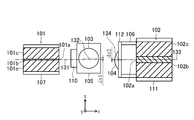
- This optical device optically connects (couples) a first optical waveguide 101 having a first end surface 101a through which light enters and exits and a second optical waveguide 102 having a second end surface 102a through which light enters and exits. It is a device to make it.
- the second end surface 102a is arranged so as to face the first end surface 101a.
- the first optical waveguide 101 and the second optical waveguide 102 are arranged so that the optical axis 131 of the first optical waveguide 101 and the optical axis 133 of the second optical waveguide 102 substantially coincide with each other. ..
- the first optical waveguide 101 is, for example, a so-called silicon optical waveguide composed of a core 101b made of Si and a clad 101c made of silicon oxide.
- the second optical waveguide 102 is a so-called optical fiber composed of a quartz-based core 102b and a clad 102c.
- This optical device includes a first lens 103, a second lens 104, and an adjustment table 105.
- the first lens 103 is arranged between the first end surface 101a and the second end surface 102a, and increases the diameter of the mode field of light emitted from the first end surface 101a by waveguideing through the first optical waveguide 101.
- the first lens 103 is, for example, a spherical (spherically symmetrical) ball lens.
- the first lens 103 is made of, for example, a quartz-based material.
- the second lens 104 is arranged between the first lens 103 and the second end surface 102a, and collects the light that has passed through the first lens 103.
- the second lens 104 is the light that has passed through the first lens 103 in order to connect the light emitted from the first end surface 101a through the first optical waveguide 101 to the second optical waveguide 102 at the second end surface 102a.
- the second lens 104 is, for example, a convex lens having a refracting surface (for example, an ellipsoidal surface) convex toward the first end surface 101a.
- the second optical waveguide 102 is placed (fixed) on the mounting table 111.
- the mounting table 111 is made of, for example, glass.
- the second lens 104 is supported and fixed to the side of the second end surface 102a of the second optical waveguide 102 by the support portion 106.
- the support portion 106 is made of, for example, a resin such as plastic.
- the second lens 104 is formed on a plate-shaped or sheet-shaped support plate 112, and is fixed to the support portion 106 via the support plate 112.
- the support plate 112 can be made of the same resin as the support portion 106.
- the adjustment table 105 places (fixes) the first lens 103 on it. Further, the adjusting table 105 adjusts the distance between the optical axis 131 of the first optical waveguide 101 and the principal point 132 of the first lens 103 on a plane perpendicular to the optical axis 131 of the first optical waveguide 101.
- the adjusting table 105 is made of, for example, the same quartz-based material as the first lens 103.
- the adjusting table 105 is fixed by the adhesive layer 109 on the base 108 on which the mounting table 107 on which the first optical waveguide 101 is placed is fixed.
- the mounting table 107 can be made of, for example, Si.
- the stop member 110 limits the movement of the adjusting table 105 in the optical axis direction.
- the decrease in coupling efficiency in the optical system due to the displacement of the second lens 104 fixedly arranged with respect to the second optical waveguide 102 can be suppressed by adjusting the position of the first lens 103 using the adjusting table 105. To do so.
- the distance between the optical axis 131 of the first optical waveguide 101 and the principal point 132 of the first lens 103 is d1
- the distance between the optical axis 133 of the second optical waveguide 102 and the principal point 134 of the second lens 104 is d2.
- the x-coordinate component of the distance d1 is dx1
- the y-coordinate component is dy1.
- the x-coordinate component of the distance d2 is dx2, and the y-coordinate component is dy2.
- FIG. 3 shows the calculation result of the optical path when the principal point of the lens is located on the optical axis of the optical waveguide. More specifically, the optical axis 131 of the core 101b of the first optical waveguide 101 and the optical axis 133 of the core 102b of the second optical waveguide 102 are coaxial, and the principal points 132 and the second of the first lens 103 This is the case where the principal point 134 of the lens 104 is located on the optical axis described above.
- the first optical waveguide 101 has a reverse taper structure in which the cross-sectional area of the core 101b decreases in the propagation (waveguide) direction, and the numerical aperture of the emitted light is about 0.3 or less.
- the mode field diameter of the waveguide light has been converted. If the numerical aperture does not exceed 0.3, the tapered structure may not be formed.
- the optical path was calculated by the ray tracing method with a numerical aperture of about 0.4 (corresponding to a full-width radiation of 50 degrees).
- the incident end face of the second optical waveguide 102 is defined as an image plane.
- the diameter of the core 102b of the second optical waveguide 102 is 10 ⁇ m.
- the y-coordinate (vertical axis) of the intersection (point image position) of the light ray and the image plane is the sine (sin ( ⁇ s)) of the angle ⁇ s formed by the emitted light ray on the light source side and the optical axis 131 and the first optical waveguide.
- NSS n1 ⁇ sin ( ⁇ s)
- the principal point of the lens is located on the optical axis of the optical waveguide, the emitted light having an NSS of about ⁇ 0.35 to 0.35 is incident on the plane of the core 102b of the second optical waveguide 102. You can see that it does.
- the product NSR (n2 ⁇ sin ( ⁇ r)) of the refractive index n2 between the second optical waveguide 102 and the second lens 104 must satisfy a value determined by the structure of the second optical waveguide 102.
- the ⁇ r corresponding to the maximum value of the NSR that can propagate through the second optical waveguide 102 is called the maximum light receiving angle ⁇ max.
- FIG. 5 shows the results of plotting with NSR on the vertical axis and NSS on the horizontal axis.
- the numerical aperture corresponding to ⁇ max is about 0.1.
- the absolute value of NSR is within 0.1 when it is incident on the second end surface 102a, so that the second optical waveguide 101 is second. It shows that it can propagate through the optical waveguide 102.
- the optical axis 131 of the core 101b of the first optical waveguide 101, the optical axis 133 of the core 102b of the second optical waveguide 102, and the principal point 132 of the first lens 103 are coaxial with each other, and the principal of the second lens 104 is The case where the point 134 deviates from the optical axis 133 will be described.
- the coupling efficiency of (shifting 134) is shown.
- the point image position shifts downward as a whole, so that the coupling efficiency deteriorates.
- the point image position (y direction) corrected by the position adjustment of the first lens 103 is plotted against the NSS.
- the dotted line ID0 corresponds to the case where the point image position is totally displaced due to the deviation of the principal point of the second lens 104.
- the solid line ID1 when the point image position is corrected by adjusting the position of the first lens 103, it can be seen that the light is focused toward the inside of the core 102b of the second optical waveguide 102.
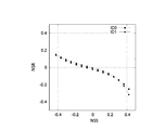
- FIG. 10 shows the relationship between NSS and NSR before and after the position adjustment of the first lens 103.
- the dotted line ID0 indicates before adjustment, and the solid line ID1 indicates after adjustment.
- the NSS can propagate in the second optical waveguide 102 having a numerical aperture of about ⁇ 0.3 to 0.25.
- the structure of the first lens 103 is rotationally symmetric with respect to the axis passing through the principal point 132 parallel to the z-axis, and as shown in FIG. 2, the deviation of the second lens 104 is in the x direction.
- the point image position can be corrected by adjusting the position of the first lens 103 on the same principle.
- This optical device further includes a transparent resin layer 113 arranged so as to fill the space between the second lens 104 and the second end surface 102a in the optical device according to the first embodiment described above.
- the space between the support plate 112 and the second end surface 102a inside the support portion 106 is filled with the transparent resin layer 113.
- the refractive index of the transparent resin layer 113 can be equal to or lower than the refractive index of the second lens 104 and the support plate 112. Further, it is desirable that the coefficient of thermal expansion of the transparent resin layer 113 is about the same as that of the support portion 106 and the support plate 112.
- the optical path length between the second lens 104 and the incident end face of the second optical waveguide 102 is made longer in order to concentrate on the core 102b than when the transparent resin layer 113 is not provided.
- FIG. 13 shows the relationship between the NSS and the point image position (y direction) after the position adjustment by the first lens 103.
- FIG. 14 shows the relationship between NSS and NSR after the position adjustment by the first lens 103. The effect of correcting the point image position by adjusting the position using the first lens 103 can be obtained in the same manner as when the transparent resin layer 113 is not provided.
- FIG. 15 shows the absolute value of the shift amount (dy1) at the principal point 132 of the first lens 103, the shift amount (dy2) of the principal point 134 of the second lens 104, and the shape of the refracting surface (convex surface) of the second lens 104.
- the horizontal axis is NSS and the vertical axis is the point image position.
- the refracting surface of the first lens 103 and the refracting surface of the second lens 104 are spherical surfaces having the same radius of curvature. It is assumed that the light beam after passing through the first lens 103 is converted into collimated light.
- the deviation correction effect of the point image position is that the absolute value of the shift amount dy1 of the first lens 103 is the shift amount dy2 of the second lens 104 between spherical lenses having the same radius of curvature. The smaller it is, the more you get. However, unfocused light rays partially remain in the core 102b (-5 ⁇ m ⁇ y ⁇ 5 ⁇ m).
- the setting of the position of the adjustment table 105 will be described below.
- the profiles of the shift amounts dx2 and dy2 of the principal point 134 of the second lens 104 are acquired in advance.
- the position of the principal point 132 of the first lens 103 is calculated by optical path calculation.
- the position of the adjusting table 105 in the y direction is adjusted by controlling the thickness of the adhesive layer 109.
- the position adjustment of the adjustment table 105 in the x direction is performed by moving the adjustment table 105 in the x direction so that the x coordinate of the principal point 132 of the first lens 103 matches the calculated position.
- the stop member 110 fixed on the base 108 prevents the adjusting table 105 from moving in the optical axis direction.
- the adjusting table 105 is directly placed (arranged) on the base 108 without using the adhesive layer, as shown in FIG. Further, the adjusting table 105 is fixed by the adhesive portion 109a arranged so as to cover the side wall of the adjusting table 105. In this case, the position adjustment of the adjustment table 105 in the y direction is performed by preparing a plurality of adjustment tables 105 having different heights and selecting the adjustment table 105 whose principal point position of the first lens 103 is closest to the calculation position. Do.
- the first optical waveguide may be an optical waveguide composed of a compound semiconductor such as indium phosphide (InP), gallium nitride (GaN), and gallium arsenide (GaAs).
- the second optical waveguide is not limited to the optical fiber, and may be a plane light wave circuit. The same applies to the first optical waveguide.
- the first lens is not limited to a ball lens but can be an aspherical lens.
- the second lens is not limited to an ellipsoidal lens, and may be another aspherical lens or a spherical lens such as a paraboloid or a hyperboloid.
- the optical axis of the first optical waveguide and the principal point of the first lens are mounted on the plane perpendicular to the optical axis of the first optical waveguide. Since an adjustment table for adjusting the distance between the lens and the optical waveguide is provided, the coupling efficiency is reduced due to the fact that the principal point of the lens and the optical axis of the core of the optical waveguide do not match in integrally forming the lens and the optical waveguide. It can be corrected, and a decrease in coupling efficiency in an optical system using a plurality of lenses can be suppressed.
Landscapes
- Physics & Mathematics (AREA)
- General Physics & Mathematics (AREA)
- Optics & Photonics (AREA)
- Optical Couplings Of Light Guides (AREA)
Abstract
The present invention provides an optical device including a first lens (103), a second lens (104), and an adjustment table (105). The first lens (103) is disposed between a first end surface (101a) and a second end surface (102a), and enlarges a mode field diameter of light guided through a first optical waveguide (101) and emitted from the first end surface (101a). The second lens (104) is disposed between the first lens (103) and the second end surface (102a) to converge light having passed through the first lens (103). The adjustment table (105) is a table on which the first lens (103) is placed. The adjustment table (105) is used to adjust a distance between the optical axis (131) of the first optical waveguide (101) and a principal point (132) of the first lens (103), on a plane perpendicular to the optical axis (131) of the first optical waveguide (101).
Description
本発明は、光学装置に関し、特に、光のモードフィールド径を変換して2つの光導波路の間を接続する光学装置に関する。
The present invention relates to an optical device, and more particularly to an optical device that converts the mode field diameter of light to connect between two optical waveguides.
光導波路の間を効率的に結合(光学的に接続)する光接続技術が求められている。例えば、通信用光源を担う化合物系の半導体光素子やシリコンフォトニクスを構成するシリコン(Si)光導波路と、光ファイバや平面光波回路(PLC)などとを、高い効率で光接続する技術が求められている。
There is a demand for an optical connection technology that efficiently couples (optically connects) between optical waveguides. For example, there is a need for a technology for highly efficient optical connection between a compound-based semiconductor optical device that plays a light source for communication and a silicon (Si) optical waveguide that constitutes silicon photonics, and an optical fiber or a planar light wave circuit (PLC). ing.
上述したような光接続では、各々の光導波路における光のモードフィールド径が大きく異なる。このため、これらの間の光接続では、テーパ構造やグレーティング構造などの、光のモードフィールド径を変換する構造が用いられている。しかしながら、モードフィールド径を変換する構造の作製ばらつきなどにより、光接続の効率(結合効率)が劣化する場合がある。この劣化を抑制するために、光路長の制約の範囲内で、レンズ光学系を構成し、結合効率を補償する技術が用いられる。
In the optical connection as described above, the mode field diameter of light in each optical waveguide is significantly different. Therefore, in the optical connection between them, a structure for converting the mode field diameter of light, such as a tapered structure or a grating structure, is used. However, the efficiency of optical connection (coupling efficiency) may deteriorate due to variations in the fabrication of the structure that converts the mode field diameter. In order to suppress this deterioration, a technique is used in which a lens optical system is configured and the coupling efficiency is compensated within the range of the optical path length constraint.
上述した結合効率を補償するためのレンズ光学系には、様々な形態がある。単レンズによる光学系は、調芯工程が簡易で、コスト削減の観点で用いられる。しかしながら、単レンズによる光学系では、戻り光の問題や、波長選択などの様々な機能を付加させることが容易ではない。
There are various forms of the lens optical system for compensating for the coupling efficiency described above. An optical system using a single lens has a simple centering process and is used from the viewpoint of cost reduction. However, in an optical system using a single lens, it is not easy to add various functions such as a problem of return light and wavelength selection.
これに対し、2枚レンズによる光学系を用いることで、戻り光の抑制や波長選択などの機能を得ることが可能となる。例えば、光接続対象の光導波路の間に、2枚レンズを用いたコリメート系を構成し、この間にアイソレーターやフィルターを配置する。ただし、このような2枚レンズによる光学系は、調芯工程が単レンズ系より増え、製造コストが増大する。このため、図17に示すように、クラッド301およびコア302による光導波路303と、レンズ304とを一体とし、レンズと光導波路との間の調芯工程を削減する構造が提案されている(特許文献1参照)。
On the other hand, by using an optical system with two lenses, it is possible to obtain functions such as suppression of return light and wavelength selection. For example, a collimating system using two lenses is constructed between the optical waveguides to be optically connected, and an isolator and a filter are arranged between them. However, in such an optical system using two lenses, the alignment process is increased as compared with the single lens system, and the manufacturing cost is increased. Therefore, as shown in FIG. 17, a structure has been proposed in which the optical waveguide 303 by the clad 301 and the core 302 and the lens 304 are integrated to reduce the alignment process between the lens and the optical waveguide (patented). Reference 1).
しかしながら、レンズと光導波路を一体形成する技術では、レンズの主点と、光導波路の光軸とを一致させることは難しく、これらの間のずれ量に対応して結合効率が低下するという問題がある。このように、結合効率を補償するための光学系で複数のレンズを用いる場合、上述したことによる結合効率の低下により、結合効率の劣化があまり補償できないという問題があった。
However, in the technique of integrally forming the lens and the optical waveguide, it is difficult to match the principal point of the lens with the optical axis of the optical waveguide, and there is a problem that the coupling efficiency decreases according to the amount of deviation between them. is there. As described above, when a plurality of lenses are used in the optical system for compensating the coupling efficiency, there is a problem that the deterioration of the coupling efficiency cannot be compensated so much due to the decrease in the coupling efficiency due to the above.
本発明は、以上のような問題点を解消するためになされたものであり、複数のレンズを用いる光学系における結合効率の低下が抑制できるようにすることを目的とする。
The present invention has been made to solve the above problems, and an object of the present invention is to suppress a decrease in coupling efficiency in an optical system using a plurality of lenses.
本発明に係る光学装置は、接続対象の一方の第1光導波路の光が入出射する第1端面と、接続対象の他方の第2光導波路の光が入出射する、第1端面に向かい合う第2端面との間に配置され、第1光導波路を導波して第1端面から出射する光のモードフィールドの径を拡大する第1レンズと、第1レンズと第2端面との間に配置され、第1レンズを通過した光を集光する第2レンズと、第1レンズが載置され、第1光導波路の光軸に垂直な平面の上で、第1光導波路の光軸と第1レンズの主点との距離を調整するための調整台と、第2レンズを第2光導波路の第2端面の側に支持する支持部とを備える。
The optical device according to the present invention has a first end surface in which the light of one first optical waveguide to be connected enters and exits, and a first end surface facing the first end surface in which the light of the other second optical waveguide to be connected enters and exits. It is placed between the first lens and the second end face, which is placed between the two end faces and expands the diameter of the mode field of the light emitted from the first end face by waveguideing through the first optical waveguide. The second lens that collects the light that has passed through the first lens and the first lens are placed on the plane perpendicular to the optical axis of the first optical waveguide, and the optical axis and the first optical waveguide of the first optical waveguide. An adjustment table for adjusting the distance from the main point of one lens and a support portion for supporting the second lens on the side of the second end surface of the second optical waveguide are provided.
以上説明したように、本発明によれば、第1レンズが載置され、第1光導波路の光軸に垂直な平面の上で、第1光導波路の光軸と第1レンズの主点との距離を調整するための調整台を備えるので、複数のレンズを用いる光学系における結合効率の低下が抑制できる。
As described above, according to the present invention, the first lens is mounted, and the optical axis of the first optical waveguide and the principal point of the first lens are formed on a plane perpendicular to the optical axis of the first optical waveguide. Since the adjustment table for adjusting the distance is provided, it is possible to suppress a decrease in coupling efficiency in an optical system using a plurality of lenses.
以下、本発明の実施の形態に係る光学装置について説明する。
Hereinafter, the optical device according to the embodiment of the present invention will be described.
[実施の形態1]
はじめに、本発明の実施の形態1に係る光学装置について、図1,図2を参照して説明する。 [Embodiment 1]
First, the optical device according to the first embodiment of the present invention will be described with reference to FIGS. 1 and 2.
はじめに、本発明の実施の形態1に係る光学装置について、図1,図2を参照して説明する。 [Embodiment 1]
First, the optical device according to the first embodiment of the present invention will be described with reference to FIGS. 1 and 2.
この光学装置は、光が入出射する第1端面101aを有する第1光導波路101と、光が入出射する第2端面102aを有する第2光導波路102との間を光学的に接続(結合)させる装置である。なお、第2端面102aは、第1端面101aに向かい合って配置されている。例えば、第1光導波路101と第2光導波路102とは、第1光導波路101の光軸131と、第2光導波路102の光軸133とが、実質的に一致するように配置されている。
This optical device optically connects (couples) a first optical waveguide 101 having a first end surface 101a through which light enters and exits and a second optical waveguide 102 having a second end surface 102a through which light enters and exits. It is a device to make it. The second end surface 102a is arranged so as to face the first end surface 101a. For example, the first optical waveguide 101 and the second optical waveguide 102 are arranged so that the optical axis 131 of the first optical waveguide 101 and the optical axis 133 of the second optical waveguide 102 substantially coincide with each other. ..
第1光導波路101は、例えば、Siからなるコア101bと、酸化シリコンからなるクラッド101cとから構成された、いわゆるシリコン光導波路である。第2光導波路102は、石英系のコア102bと、クラッド102cとから構成された、いわゆる光ファイバである。
The first optical waveguide 101 is, for example, a so-called silicon optical waveguide composed of a core 101b made of Si and a clad 101c made of silicon oxide. The second optical waveguide 102 is a so-called optical fiber composed of a quartz-based core 102b and a clad 102c.
この光学装置は、第1レンズ103、第2レンズ104、および調整台105を備える。
This optical device includes a first lens 103, a second lens 104, and an adjustment table 105.
第1レンズ103は、第1端面101aと第2端面102aとの間に配置され、第1光導波路101を導波して第1端面101aから出射する光のモードフィールドの径を拡大する。第1レンズ103は、例えば、球状(球対称)のボールレンズである。第1レンズ103は、例えば、石英系の材料から構成されている。
The first lens 103 is arranged between the first end surface 101a and the second end surface 102a, and increases the diameter of the mode field of light emitted from the first end surface 101a by waveguideing through the first optical waveguide 101. The first lens 103 is, for example, a spherical (spherically symmetrical) ball lens. The first lens 103 is made of, for example, a quartz-based material.
第2レンズ104は、第1レンズ103と第2端面102aとの間に配置され、第1レンズ103を通過した光を集光する。第2レンズ104は、第1光導波路101を導波して第1端面101aから出射する光を、第2端面102aで第2光導波路102に結合させるために、第1レンズ103を通過した光を集光する。第2レンズ104は、例えば、第1端面101aに向かって凸な屈折面(例えば楕円面)を有する凸レンズである。なお、第2光導波路102は、載置台111の上に載置(固定)されている。載置台111は、例えば、ガラスから構成されている。
The second lens 104 is arranged between the first lens 103 and the second end surface 102a, and collects the light that has passed through the first lens 103. The second lens 104 is the light that has passed through the first lens 103 in order to connect the light emitted from the first end surface 101a through the first optical waveguide 101 to the second optical waveguide 102 at the second end surface 102a. Condenses. The second lens 104 is, for example, a convex lens having a refracting surface (for example, an ellipsoidal surface) convex toward the first end surface 101a. The second optical waveguide 102 is placed (fixed) on the mounting table 111. The mounting table 111 is made of, for example, glass.
ここで、第2レンズ104は、支持部106により、第2光導波路102の第2端面102aの側に支持および固定されている。支持部106は、例えば、プラスチックなどの樹脂から構成されている。なお、この例では、第2レンズ104は、板状またはシート状の支持板112の上に形成され、支持板112を介して支持部106に固定されている。支持板112は、支持部106と同じ樹脂から構成することができる。
Here, the second lens 104 is supported and fixed to the side of the second end surface 102a of the second optical waveguide 102 by the support portion 106. The support portion 106 is made of, for example, a resin such as plastic. In this example, the second lens 104 is formed on a plate-shaped or sheet-shaped support plate 112, and is fixed to the support portion 106 via the support plate 112. The support plate 112 can be made of the same resin as the support portion 106.
調整台105は、この上に第1レンズ103を載置(固定)する。また、調整台105により、第1光導波路101の光軸131に垂直な平面の上で、第1光導波路101の光軸131と第1レンズ103の主点132との距離を調整する。調整台105は、例えば、第1レンズ103と同じ石英系の材料から構成されている。例えば、第1光導波路101を載置する載置台107が固定される基盤108の上に、接着層109により調整台105を固定する。載置台107は、例えば、Siから構成することができる。接着層109の厚さにより調整台105の位置を調整することで、光軸131と主点132との距離が調整できる。また、停止部材110により、調整台105の光軸方向の移動を制限する。
The adjustment table 105 places (fixes) the first lens 103 on it. Further, the adjusting table 105 adjusts the distance between the optical axis 131 of the first optical waveguide 101 and the principal point 132 of the first lens 103 on a plane perpendicular to the optical axis 131 of the first optical waveguide 101. The adjusting table 105 is made of, for example, the same quartz-based material as the first lens 103. For example, the adjusting table 105 is fixed by the adhesive layer 109 on the base 108 on which the mounting table 107 on which the first optical waveguide 101 is placed is fixed. The mounting table 107 can be made of, for example, Si. By adjusting the position of the adjusting table 105 according to the thickness of the adhesive layer 109, the distance between the optical axis 131 and the principal point 132 can be adjusted. Further, the stop member 110 limits the movement of the adjusting table 105 in the optical axis direction.
実施の形態1では、第2光導波路102に対して固定配置される第2レンズ104のずれによる光学系における結合効率の低下を、調整台105を用いた第1レンズ103の位置調整により抑制できるようにする。
In the first embodiment, the decrease in coupling efficiency in the optical system due to the displacement of the second lens 104 fixedly arranged with respect to the second optical waveguide 102 can be suppressed by adjusting the position of the first lens 103 using the adjusting table 105. To do so.
以下、上述した第1レンズ103の位置調整による光学系における結合効率の低下抑制について、より詳細に説明する。まず、実施の形態1における光学装置の光路の計算結果について説明する。以下では、第1光導波路101の光軸131と第1レンズ103の主点132との距離をd1、第2光導波路102の光軸133と第2レンズ104の主点134との距離をd2とする。ここで、距離d1のx座標の成分をdx1とし、y座標の成分をdy1とする。また、距離d2のx座標の成分をdx2とし、y座標の成分をdy2とする。
Hereinafter, the suppression of the decrease in coupling efficiency in the optical system by adjusting the position of the first lens 103 described above will be described in more detail. First, the calculation result of the optical path of the optical device according to the first embodiment will be described. In the following, the distance between the optical axis 131 of the first optical waveguide 101 and the principal point 132 of the first lens 103 is d1, and the distance between the optical axis 133 of the second optical waveguide 102 and the principal point 134 of the second lens 104 is d2. And. Here, the x-coordinate component of the distance d1 is dx1, and the y-coordinate component is dy1. Further, the x-coordinate component of the distance d2 is dx2, and the y-coordinate component is dy2.
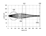
図3は、レンズの主点が、光導波路の光軸上に位置する場合の、光路の計算結果を示す。より詳細には、第1光導波路101のコア101bの光軸131と、第2光導波路102のコア102bの光軸133が同軸上にあり、且つ、第1レンズ103の主点132と第2レンズ104の主点134が、上述した光軸上に位置する場合である。
FIG. 3 shows the calculation result of the optical path when the principal point of the lens is located on the optical axis of the optical waveguide. More specifically, the optical axis 131 of the core 101b of the first optical waveguide 101 and the optical axis 133 of the core 102b of the second optical waveguide 102 are coaxial, and the principal points 132 and the second of the first lens 103 This is the case where the principal point 134 of the lens 104 is located on the optical axis described above.
なお、第1光導波路101は、伝搬(導波)方向に向かってコア101bの断面積が減少する逆テーパ構造を有し、出射光の開口数が、約0.3以下になるように、導波光のモードフィールド径が変換されている。上記の開口数が0.3を超過しなければ、テーパ構造を形成しなくても構わない。光路計算は、開口数を約0.4(放射全角50度に相当)として光線追跡法によって行った。第2光導波路102の入射端面を像面と定義する。第2光導波路102のコア102bの直径を10μmとする。
The first optical waveguide 101 has a reverse taper structure in which the cross-sectional area of the core 101b decreases in the propagation (waveguide) direction, and the numerical aperture of the emitted light is about 0.3 or less. The mode field diameter of the waveguide light has been converted. If the numerical aperture does not exceed 0.3, the tapered structure may not be formed. The optical path was calculated by the ray tracing method with a numerical aperture of about 0.4 (corresponding to a full-width radiation of 50 degrees). The incident end face of the second optical waveguide 102 is defined as an image plane. The diameter of the core 102b of the second optical waveguide 102 is 10 μm.
図4は、光線と像面の交点(点像位置)のy座標(縦軸)を、光源側の出射光線と光軸131の成す角θsの正弦(sin(θs))と第1光導波路101と第1レンズ103との間の屈折率n1の積NSS(n1・sin(θs))(横軸)に対してプロットした結果を示す。これにより、レンズの主点が光導波路の光軸上に位置していれば、NSSが-0.35から0.35程度の出射光は、第2光導波路102のコア102bの面内に入射することがわかる。
In FIG. 4, the y-coordinate (vertical axis) of the intersection (point image position) of the light ray and the image plane is the sine (sin (θs)) of the angle θs formed by the emitted light ray on the light source side and the optical axis 131 and the first optical waveguide. The result of plotting with respect to the product NSS (n1 · sin (θs)) (horizontal axis) of the refractive index n1 between 101 and the first lens 103 is shown. As a result, if the principal point of the lens is located on the optical axis of the optical waveguide, the emitted light having an NSS of about −0.35 to 0.35 is incident on the plane of the core 102b of the second optical waveguide 102. You can see that it does.
さらに、入射した光が第2光導波路102を光が伝搬するためには、第2光導波路102の第2端面102aへの入射光線と、光軸133の成す角θrの正弦(sin(θr))と、第2光導波路102と第2レンズ104との間の屈折率n2の積NSR(n2・sin(θr))が、第2光導波路102の構造によって決まる値を満たす必要がある。第2光導波路102を伝搬可能なNSRの最大値に相当するθrを、最大受光角θmaxと呼ぶ。
Further, in order for the incident light to propagate through the second optical waveguide 102, the incident light beam on the second end surface 102a of the second optical waveguide 102 and the sinusoidal angle θr formed by the optical axis 133 (sin (θr)). ) And the product NSR (n2 · sin (θr)) of the refractive index n2 between the second optical waveguide 102 and the second lens 104 must satisfy a value determined by the structure of the second optical waveguide 102. The θr corresponding to the maximum value of the NSR that can propagate through the second optical waveguide 102 is called the maximum light receiving angle θ max.
図5は、縦軸をNSR、横軸をNSSとしてプロットした結果を示す。コア102bの屈折率を1.47、屈折率差0.3%とすれば、θmaxに相当する開口数は、約0.1である。第1光導波路101の出射光は、NSSが-0.35から0.35程度であれば、第2端面102aへの入射において、NSRの絶対値が、0.1以内であるから、第2光導波路102を伝搬可能であることを示す。
FIG. 5 shows the results of plotting with NSR on the vertical axis and NSS on the horizontal axis. Assuming that the refractive index of the core 102b is 1.47 and the refractive index difference is 0.3%, the numerical aperture corresponding to θ max is about 0.1. When the NSS of the emitted light of the first optical waveguide 101 is about −0.35 to 0.35, the absolute value of NSR is within 0.1 when it is incident on the second end surface 102a, so that the second optical waveguide 101 is second. It shows that it can propagate through the optical waveguide 102.
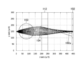
次に、第1光導波路101のコア101bの光軸131と、第2光導波路102のコア102bの光軸133、第1レンズ103の主点132が同軸上にあり、第2レンズ104の主点134が、光軸133上からずれている場合について説明する。
Next, the optical axis 131 of the core 101b of the first optical waveguide 101, the optical axis 133 of the core 102b of the second optical waveguide 102, and the principal point 132 of the first lens 103 are coaxial with each other, and the principal of the second lens 104 is The case where the point 134 deviates from the optical axis 133 will be described.
図6は、dy2=0としてdy1を変化させた場合(第1レンズ103の主点132をシフト)の結合効率、および、dy1=0としてdy2を変化させた場合(第2レンズ104の主点134をシフト)の結合効率を示す。結合効率は、dy1=dy2=0における第2光導波路102の入射端面内に分布するモードと、dy1またはdy2がシフトした場合のモードの重なり積分から求めた値をdB単位で表している。
FIG. 6 shows the coupling efficiency when dy1 is changed when dy2 = 0 (the principal point 132 of the first lens 103 is shifted) and when dy2 is changed when dy1 = 0 (the principal point of the second lens 104). The coupling efficiency of (shifting 134) is shown. The coupling efficiency is expressed in dB as a value obtained from the overlap integral of the mode distributed in the incident end face of the second optical waveguide 102 at dy1 = dy2 = 0 and the mode when dy1 or dy2 is shifted.
図7は、dy1=0、dy2=-5μmの状態で、点像位置のy座標(縦軸)を、NSS(横軸)に対して光路計算した結果を示す。この場合、点像位置が全体的に下方にシフトするため結合効率が劣化する。
FIG. 7 shows the result of optical path calculation of the y coordinate (vertical axis) of the point image position with respect to NSS (horizontal axis) in the state of dy1 = 0 and dy2 = -5 μm. In this case, the point image position shifts downward as a whole, so that the coupling efficiency deteriorates.
図8は、dy1=+2.5μm、dy2=-5μmの状態で、図3と同様に光路計算した結果を示す。第1レンズ103を第2レンズ104と逆方向に位置調整させることで、第2レンズ104のずれによる点像位置のずれを補正している。結合効率は、第1レンズ103のシフト量に対して敏感に変化するため、dy1の絶対値は、dy2のそれより小さい。すなわち、第1レンズ103と第2レンズ104の位置関係は、次式を満たす。
FIG. 8 shows the results of optical path calculation in the same manner as in FIG. 3 in the state of dy1 = + 2.5 μm and dy2 = -5 μm. By adjusting the position of the first lens 103 in the direction opposite to that of the second lens 104, the deviation of the point image position due to the deviation of the second lens 104 is corrected. Since the coupling efficiency changes sensitively with respect to the shift amount of the first lens 103, the absolute value of dy1 is smaller than that of dy2. That is, the positional relationship between the first lens 103 and the second lens 104 satisfies the following equation.
dy1×dy2<0・・・(1)
|dy1|<|dy2|・・・(2) dy1 x dy2 <0 ... (1)
| dy1 | < | dy2 | ・ ・ ・ (2)
|dy1|<|dy2|・・・(2) dy1 x dy2 <0 ... (1)
| dy1 | < | dy2 | ・ ・ ・ (2)
図9に、第1レンズ103の位置調整により補正された点像位置(y方向)を、NSSに対してプロットした。点線ID0は、第2レンズ104の主点ずれにより点像位置が全体的にずれている場合に相当する。これに対し、実線ID1に示すように、第1レンズ103の位置調整により、点像位置が補正されると、第2光導波路102のコア102bの内部に向かって集光されることがわかる。
In FIG. 9, the point image position (y direction) corrected by the position adjustment of the first lens 103 is plotted against the NSS. The dotted line ID0 corresponds to the case where the point image position is totally displaced due to the deviation of the principal point of the second lens 104. On the other hand, as shown by the solid line ID1, when the point image position is corrected by adjusting the position of the first lens 103, it can be seen that the light is focused toward the inside of the core 102b of the second optical waveguide 102.
図10は、第1レンズ103の位置調整前後における、NSSとNSRの関係を示す。点線ID0は調整前、実線ID1は、調整後を示す。NSSが、-0.3から0.25程度で、開口数0.1の第2光導波路102内を伝搬させることが可能である。本実施の形態1では、第1レンズ103の構造は、z軸に平行な主点132を通る軸に対して回転対称であり、図2に示すように、第2レンズ104のずれがx方向である場合も、同様の原理で、第1レンズ103の位置調整により、点像位置の補正が可能である。
FIG. 10 shows the relationship between NSS and NSR before and after the position adjustment of the first lens 103. The dotted line ID0 indicates before adjustment, and the solid line ID1 indicates after adjustment. The NSS can propagate in the second optical waveguide 102 having a numerical aperture of about −0.3 to 0.25. In the first embodiment, the structure of the first lens 103 is rotationally symmetric with respect to the axis passing through the principal point 132 parallel to the z-axis, and as shown in FIG. 2, the deviation of the second lens 104 is in the x direction. In this case as well, the point image position can be corrected by adjusting the position of the first lens 103 on the same principle.
[実施の形態2]
次に、本発明の実施の形態2に係る光学装置について、図11を参照して説明する。この光学装置は、前述した実施の形態1に係る光学装置に、さらに、第2レンズ104と第2端面102aとの間を埋めるように配置された透明樹脂層113を備える。例えば、支持部106の内側の、支持板112と第2端面102aとの間が、透明樹脂層113で充填されている。透明樹脂層113を設けることで、支持部106と第2光導波路102の端面との間の接合状態が安定化する。例えば、透明樹脂層113の屈折率は、第2レンズ104および支持板112の屈折率以下とすることができる。また、透明樹脂層113の熱膨張係数は、支持部106および支持板112と同程度であることが望ましい。 [Embodiment 2]
Next, the optical device according to the second embodiment of the present invention will be described with reference to FIG. This optical device further includes atransparent resin layer 113 arranged so as to fill the space between the second lens 104 and the second end surface 102a in the optical device according to the first embodiment described above. For example, the space between the support plate 112 and the second end surface 102a inside the support portion 106 is filled with the transparent resin layer 113. By providing the transparent resin layer 113, the bonding state between the support portion 106 and the end face of the second optical waveguide 102 is stabilized. For example, the refractive index of the transparent resin layer 113 can be equal to or lower than the refractive index of the second lens 104 and the support plate 112. Further, it is desirable that the coefficient of thermal expansion of the transparent resin layer 113 is about the same as that of the support portion 106 and the support plate 112.
次に、本発明の実施の形態2に係る光学装置について、図11を参照して説明する。この光学装置は、前述した実施の形態1に係る光学装置に、さらに、第2レンズ104と第2端面102aとの間を埋めるように配置された透明樹脂層113を備える。例えば、支持部106の内側の、支持板112と第2端面102aとの間が、透明樹脂層113で充填されている。透明樹脂層113を設けることで、支持部106と第2光導波路102の端面との間の接合状態が安定化する。例えば、透明樹脂層113の屈折率は、第2レンズ104および支持板112の屈折率以下とすることができる。また、透明樹脂層113の熱膨張係数は、支持部106および支持板112と同程度であることが望ましい。 [Embodiment 2]
Next, the optical device according to the second embodiment of the present invention will be described with reference to FIG. This optical device further includes a
ここで、実施の形態2に係る光学装置において、dy1=+2.5μm、dy2=-5μmとして光路計算した結果について、図12に示す。第2レンズ104と第2光導波路102の入射端面との間の光路長は、コア102bに集光するためには、透明樹脂層113を設けない場合よりも長くする。
Here, in the optical device according to the second embodiment, the results of optical path calculation with dy1 = + 2.5 μm and dy2 = -5 μm are shown in FIG. The optical path length between the second lens 104 and the incident end face of the second optical waveguide 102 is made longer in order to concentrate on the core 102b than when the transparent resin layer 113 is not provided.
次に、第1レンズ103による位置調整をした後におけるNSSと点像位置(y方向)の関係を図13に示す。また、第1レンズ103による位置調整後におけるNSSとNSRの関係を、図14に示す。第1レンズ103を用いた位置調整による点像位置の補正効果は、透明樹脂層113を設けない場合と同様に得られる。
Next, FIG. 13 shows the relationship between the NSS and the point image position (y direction) after the position adjustment by the first lens 103. Further, FIG. 14 shows the relationship between NSS and NSR after the position adjustment by the first lens 103. The effect of correcting the point image position by adjusting the position using the first lens 103 can be obtained in the same manner as when the transparent resin layer 113 is not provided.
図15に、第1レンズ103の主点132にシフト量(dy1)と、第2レンズ104の主点134のシフト量(dy2)の絶対値、および第2レンズ104の屈折面(凸面)形状により点像位置の違いを示す。図15において、横軸はNSS、縦軸は点像位置である。図15において、四角は、dy1=5.0μm、dy2=-5.0μm、三角は、dy1=3.2μm,dy2=-5.0μmの場合を示す。また、第1レンズ103の屈折面、および第2レンズ104の屈折面は、それぞれ曲率半径が等しい球面である。第1レンズ103を透過した後の光線は、コリメート光に近く変換されているものとする。
FIG. 15 shows the absolute value of the shift amount (dy1) at the principal point 132 of the first lens 103, the shift amount (dy2) of the principal point 134 of the second lens 104, and the shape of the refracting surface (convex surface) of the second lens 104. Indicates the difference in point image position. In FIG. 15, the horizontal axis is NSS and the vertical axis is the point image position. In FIG. 15, the square indicates the case of dy1 = 5.0 μm and dy2 = −5.0 μm, and the triangle indicates the case of dy1 = 3.2 μm and dy2 = −5.0 μm. Further, the refracting surface of the first lens 103 and the refracting surface of the second lens 104 are spherical surfaces having the same radius of curvature. It is assumed that the light beam after passing through the first lens 103 is converted into collimated light.
図15の四角と三角との比較から、点像位置のずれ補正効果は、曲率半径が等しい球面レンズ間において、第1レンズ103のシフト量dy1の絶対値が、第2レンズ104のシフト量dy2のそれより小さい方が、より得られる。ただし、コア102b内(-5μm<y<5μm)に集光されていない光線が部分的に残存する。
From the comparison between the square and the triangle in FIG. 15, the deviation correction effect of the point image position is that the absolute value of the shift amount dy1 of the first lens 103 is the shift amount dy2 of the second lens 104 between spherical lenses having the same radius of curvature. The smaller it is, the more you get. However, unfocused light rays partially remain in the core 102b (-5 μm <y <5 μm).
次に、図15において、丸は、三角と同じ条件dy1=3.2μm,dy2=-5.0μmにおいて、第2レンズ104のz方向の半径のみを適量大きくした場合、すなわち、第2レンズ104を、z方向を長軸とする楕円面レンズとした場合を示す。三角と丸との比較から、第2レンズ104の屈折面を楕円面にすることで、部分的に集光性能を高めることができる。
Next, in FIG. 15, the circle is the case where only the radius of the second lens 104 in the z direction is appropriately increased under the same conditions as the triangle, dy1 = 3.2 μm and dy2 = −5.0 μm, that is, the second lens 104. Is an ellipsoidal lens whose major axis is the z direction. From the comparison between the triangle and the circle, the light collection performance can be partially improved by making the refraction surface of the second lens 104 an ellipsoidal surface.
以下、調整台105の位置の設定について説明する。まず、第2レンズ104の主点134のシフト量dx2およびdy2のプロファイルを予め取得しておく。このプロファイルを参照し、光路計算によって、第1レンズ103の主点132の位置を算出する。
The setting of the position of the adjustment table 105 will be described below. First, the profiles of the shift amounts dx2 and dy2 of the principal point 134 of the second lens 104 are acquired in advance. With reference to this profile, the position of the principal point 132 of the first lens 103 is calculated by optical path calculation.
調整台105のy方向の位置調整は、接着層109の厚さ制御によって行う。調整台105のx方向の位置調整は、第1レンズ103の主点132のx座標が、計算された位置と一致するように、調整台105をx方向に移動することによって行う。基盤108の上に固定されている停止部材110により、調整台105が光軸方向に移動することが防がれている。
The position of the adjusting table 105 in the y direction is adjusted by controlling the thickness of the adhesive layer 109. The position adjustment of the adjustment table 105 in the x direction is performed by moving the adjustment table 105 in the x direction so that the x coordinate of the principal point 132 of the first lens 103 matches the calculated position. The stop member 110 fixed on the base 108 prevents the adjusting table 105 from moving in the optical axis direction.
接着層109の硬化収縮の影響を無視できない場合、図16に示すように、接着層を用いずに、調整台105を基盤108の上に直接載置(配置)する。また、調整台105の固定は、調整台105の側壁を覆うように配置された接着部109aにより行う。この場合、調整台105のy方向の位置調整は、高さが異なる調整台105を複数準備し、第1レンズ103の主点位置が、計算位置に最も近くなる調整台105を選択することにより行う。
When the influence of the curing shrinkage of the adhesive layer 109 cannot be ignored, the adjusting table 105 is directly placed (arranged) on the base 108 without using the adhesive layer, as shown in FIG. Further, the adjusting table 105 is fixed by the adhesive portion 109a arranged so as to cover the side wall of the adjusting table 105. In this case, the position adjustment of the adjustment table 105 in the y direction is performed by preparing a plurality of adjustment tables 105 having different heights and selecting the adjustment table 105 whose principal point position of the first lens 103 is closest to the calculation position. Do.
なお、第1光導波路は、リン化インジウム(InP)、窒化ガリウム(GaN)、およびヒ化ガリウム(GaAs)などの化合物系半導体から構成された光導波路とすることもできる。また、第2光導波路は、光ファイバに限るものではなく、平面光波回路とすることもできる。第1光導波路についても同様である。
The first optical waveguide may be an optical waveguide composed of a compound semiconductor such as indium phosphide (InP), gallium nitride (GaN), and gallium arsenide (GaAs). Further, the second optical waveguide is not limited to the optical fiber, and may be a plane light wave circuit. The same applies to the first optical waveguide.
また、第1レンズは、ボールレンズに限らず非球面レンズとすることもできる。また、第2レンズは、楕円面レンズに限らず、放物面や双曲面など、他の非球面レンズや球面レンズとすることもできる。
Further, the first lens is not limited to a ball lens but can be an aspherical lens. Further, the second lens is not limited to an ellipsoidal lens, and may be another aspherical lens or a spherical lens such as a paraboloid or a hyperboloid.
以上に説明したように、本発明によれば、第1レンズが載置され、第1光導波路の光軸に垂直な平面の上で、第1光導波路の光軸と第1レンズの主点との距離を調整するための調整台を備えるので、レンズと光導波路を一体形成する上で、レンズの主点と、光導波路のコアの光軸が一致していないことによる結合効率の低下を補正でき、複数のレンズを用いる光学系における結合効率の低下が抑制できるようになる。
As described above, according to the present invention, the optical axis of the first optical waveguide and the principal point of the first lens are mounted on the plane perpendicular to the optical axis of the first optical waveguide. Since an adjustment table for adjusting the distance between the lens and the optical waveguide is provided, the coupling efficiency is reduced due to the fact that the principal point of the lens and the optical axis of the core of the optical waveguide do not match in integrally forming the lens and the optical waveguide. It can be corrected, and a decrease in coupling efficiency in an optical system using a plurality of lenses can be suppressed.
なお、本発明は以上に説明した実施の形態に限定されるものではなく、本発明の技術的思想内で、当分野において通常の知識を有する者により、多くの変形および組み合わせが実施可能であることは明白である。
The present invention is not limited to the embodiments described above, and many modifications and combinations can be carried out by a person having ordinary knowledge in the art within the technical idea of the present invention. That is clear.
101…第1光導波路、101a…第1端面、101b…コア、101c…クラッド、102…第2光導波路、102a…第2端面、102b…コア、102c…クラッド、103…第1レンズ、104…第2レンズ、105…調整台、106…支持部、107…載置台、108…基盤、109…接着層、110…停止部材、111…載置台、112…支持板、113…透明樹脂層、131…光軸、132…主点、133…光軸、134…主点。
101 ... 1st optical waveguide, 101a ... 1st end face, 101b ... core, 101c ... clad, 102 ... 2nd optical waveguide, 102a ... 2nd end face, 102b ... core, 102c ... clad, 103 ... 1st lens, 104 ... Second lens, 105 ... Adjustment table, 106 ... Support part, 107 ... Mounting table, 108 ... Base, 109 ... Adhesive layer, 110 ... Stop member, 111 ... Mounting table, 112 ... Support plate, 113 ... Transparent resin layer, 131 ... optical axis, 132 ... principal point, 133 ... optical axis, 134 ... principal point.
Claims (5)
- 接続対象の一方の第1光導波路の光が入出射する第1端面と、接続対象の他方の第2光導波路の光が入出射する、前記第1端面に向かい合う第2端面との間に配置され、前記第1光導波路を導波して前記第1端面から出射する光のモードフィールドの径を拡大する第1レンズと、
前記第1レンズと前記第2端面との間に配置され、前記第1レンズを通過した光を集光する第2レンズと、
前記第1レンズが載置され、前記第1光導波路の光軸に垂直な平面の上で、前記第1光導波路の光軸と前記第1レンズの主点との距離を調整するための調整台と、
前記第2レンズを前記第2光導波路の前記第2端面の側に支持する支持部と
を備える光学装置。 Arranged between the first end face where the light of one first optical waveguide to be connected enters and exits and the second end surface facing the first end surface where the light of the other second optical waveguide to be connected enters and exits. A first lens that is guided through the first optical waveguide to increase the diameter of the mode field of light emitted from the first end face.
A second lens arranged between the first lens and the second end surface and condensing light that has passed through the first lens, and a second lens.
Adjustment for adjusting the distance between the optical axis of the first optical waveguide and the principal point of the first lens on a plane on which the first lens is placed and perpendicular to the optical axis of the first optical waveguide. With a stand,
An optical device including a support portion that supports the second lens on the side of the second end surface of the second optical waveguide. - 請求項1記載の光学装置において、
前記第2レンズは、前記第1光導波路を導波して前記第1端面から出射する光を、前記第2端面で前記第2光導波路に結合させるために、前記第1レンズを通過した光を集光する
ことを特徴とする光学装置。 In the optical device according to claim 1,
The second lens is the light that has passed through the first lens in order to connect the light emitted from the first end surface through the first optical waveguide to the second optical waveguide at the second end surface. An optical device characterized by condensing light. - 請求項1または2記載の光学装置において、
前記第1光導波路の光軸と前記第1レンズの主点との距離d1は、前記第2光導波路の光軸と前記第2レンズの主点との距離d2に対し、d1×d2<0および|d1|<|d2|が満たされる範囲とされている
ことを特徴とする光学装置。 In the optical device according to claim 1 or 2.
The distance d1 between the optical axis of the first optical waveguide and the principal point of the first lens is d1 × d2 <0 with respect to the distance d2 between the optical axis of the second optical waveguide and the principal point of the second lens. An optical device characterized in that the range in which | d1 | << | d2 | is satisfied. - 請求項1~3のいずれか1項に記載の光学装置において、
前記第1レンズは、ボールレンズであることを特徴とする光学装置。 In the optical device according to any one of claims 1 to 3.
The first lens is an optical device characterized by being a ball lens. - 請求項1~4のいずれか1項に記載の光学装置において、
前記第2レンズと前記第2端面との間を埋めるように配置された透明樹脂層をさらに備えることを特徴とする光学装置。 In the optical device according to any one of claims 1 to 4.
An optical device further comprising a transparent resin layer arranged so as to fill the space between the second lens and the second end surface.
Priority Applications (3)
| Application Number | Priority Date | Filing Date | Title |
|---|---|---|---|
| US17/774,980 US20220390679A1 (en) | 2019-11-13 | 2019-11-13 | Optical Device |
| JP2021555695A JPWO2021095164A1 (en) | 2019-11-13 | 2019-11-13 | |
| PCT/JP2019/044532 WO2021095164A1 (en) | 2019-11-13 | 2019-11-13 | Optical device |
Applications Claiming Priority (1)
| Application Number | Priority Date | Filing Date | Title |
|---|---|---|---|
| PCT/JP2019/044532 WO2021095164A1 (en) | 2019-11-13 | 2019-11-13 | Optical device |
Publications (1)
| Publication Number | Publication Date |
|---|---|
| WO2021095164A1 true WO2021095164A1 (en) | 2021-05-20 |
Family
ID=75912068
Family Applications (1)
| Application Number | Title | Priority Date | Filing Date |
|---|---|---|---|
| PCT/JP2019/044532 WO2021095164A1 (en) | 2019-11-13 | 2019-11-13 | Optical device |
Country Status (3)
| Country | Link |
|---|---|
| US (1) | US20220390679A1 (en) |
| JP (1) | JPWO2021095164A1 (en) |
| WO (1) | WO2021095164A1 (en) |
Citations (9)
| Publication number | Priority date | Publication date | Assignee | Title |
|---|---|---|---|---|
| JPS56172811U (en) * | 1980-05-21 | 1981-12-21 | ||
| JPH05113518A (en) * | 1991-10-21 | 1993-05-07 | Fujitsu Ltd | Optical fiber coupling lens system |
| JPH0933761A (en) * | 1995-07-18 | 1997-02-07 | Shinko Electric Ind Co Ltd | Optical module |
| JP2002141607A (en) * | 2000-11-02 | 2002-05-17 | Furukawa Electric Co Ltd:The | Semiconductor laser module and optical amplifier comprising it |
| JP2008250051A (en) * | 2007-03-30 | 2008-10-16 | Konica Minolta Opto Inc | Optical element unit |
| JP2008250050A (en) * | 2007-03-30 | 2008-10-16 | Konica Minolta Opto Inc | Optical device unit |
| US20140226990A1 (en) * | 2013-02-08 | 2014-08-14 | Avago Technologies General Ip (Singapore) Pte. Ltd. | Optical Communication Systems and Methods for Minimizing Reflective Feedback |
| JP2017134225A (en) * | 2016-01-27 | 2017-08-03 | 日本電信電話株式会社 | Optical waveguide |
| US20190258175A1 (en) * | 2016-11-02 | 2019-08-22 | Karlsruhe Institute Of Technology | Method for producing an optical system and optical system |
Family Cites Families (8)
| Publication number | Priority date | Publication date | Assignee | Title |
|---|---|---|---|---|
| US2131738A (en) * | 1936-03-30 | 1938-10-04 | Gulf Research Development Co | Optical system |
| US4493212A (en) * | 1982-09-20 | 1985-01-15 | Aetna Telecommunications Laboratories | Fiber optic mass sensor |
| JP2002014048A (en) * | 2000-06-27 | 2002-01-18 | Nec Miyagi Ltd | Scope and method for confirming state of connection end face of optical connector |
| JP3866585B2 (en) * | 2002-02-14 | 2007-01-10 | 日本板硝子株式会社 | Manufacturing method of filter module |
| US6868736B2 (en) * | 2002-02-22 | 2005-03-22 | Sentec Corporation | Ultra-miniature optical pressure sensing system |
| GB2428490B (en) * | 2005-07-19 | 2009-06-17 | Gigacom Holding Ab | Optical assembly |
| KR102359959B1 (en) * | 2014-03-06 | 2022-02-09 | 소니그룹주식회사 | Optical connector, cable, and optical communication device |
| JP7211235B2 (en) * | 2019-04-15 | 2023-01-24 | 日本電信電話株式会社 | optical connection structure |
-
2019
- 2019-11-13 US US17/774,980 patent/US20220390679A1/en active Pending
- 2019-11-13 WO PCT/JP2019/044532 patent/WO2021095164A1/en active Application Filing
- 2019-11-13 JP JP2021555695A patent/JPWO2021095164A1/ja active Pending
Patent Citations (9)
| Publication number | Priority date | Publication date | Assignee | Title |
|---|---|---|---|---|
| JPS56172811U (en) * | 1980-05-21 | 1981-12-21 | ||
| JPH05113518A (en) * | 1991-10-21 | 1993-05-07 | Fujitsu Ltd | Optical fiber coupling lens system |
| JPH0933761A (en) * | 1995-07-18 | 1997-02-07 | Shinko Electric Ind Co Ltd | Optical module |
| JP2002141607A (en) * | 2000-11-02 | 2002-05-17 | Furukawa Electric Co Ltd:The | Semiconductor laser module and optical amplifier comprising it |
| JP2008250051A (en) * | 2007-03-30 | 2008-10-16 | Konica Minolta Opto Inc | Optical element unit |
| JP2008250050A (en) * | 2007-03-30 | 2008-10-16 | Konica Minolta Opto Inc | Optical device unit |
| US20140226990A1 (en) * | 2013-02-08 | 2014-08-14 | Avago Technologies General Ip (Singapore) Pte. Ltd. | Optical Communication Systems and Methods for Minimizing Reflective Feedback |
| JP2017134225A (en) * | 2016-01-27 | 2017-08-03 | 日本電信電話株式会社 | Optical waveguide |
| US20190258175A1 (en) * | 2016-11-02 | 2019-08-22 | Karlsruhe Institute Of Technology | Method for producing an optical system and optical system |
Also Published As
| Publication number | Publication date |
|---|---|
| JPWO2021095164A1 (en) | 2021-05-20 |
| US20220390679A1 (en) | 2022-12-08 |
Similar Documents
| Publication | Publication Date | Title |
|---|---|---|
| JP2006208929A (en) | Optical power monitor and its manufacturing method | |
| US11934011B2 (en) | Optical connecting structure | |
| WO2011135877A1 (en) | Optical element and optical device provided with same | |
| US10649147B2 (en) | Optical module | |
| KR102100312B1 (en) | Optical fiber and optical coupler with lens | |
| JP6359848B2 (en) | Optical receptacle and optical module having the same | |
| WO2019176181A1 (en) | Laser module | |
| CN108508544B (en) | Optical coupling system and optical coupling method | |
| WO2020213411A1 (en) | Optical connecting structure | |
| WO2021095164A1 (en) | Optical device | |
| JP4146196B2 (en) | Composite optical device and manufacturing method thereof | |
| JP6495640B2 (en) | Optical communication device and method of manufacturing optical communication device | |
| WO2019244554A1 (en) | Planar lightwave circuit and optical device | |
| JP5546410B2 (en) | Optical member, optical communication module using the same, and alignment method | |
| US20030058414A1 (en) | Ghost image prevention element for imaging optical system | |
| JP2017134228A (en) | Optical waveguide | |
| US11156780B2 (en) | Optical system | |
| JP2019117394A (en) | Optical communication device and manufacturing method therefor | |
| US20230082895A1 (en) | Optical device provided with a plurality of lenses | |
| JP2020052067A (en) | Optical waveguide module | |
| JP2002236261A (en) | Variable group delay unit and variable group delay module | |
| JP5499258B1 (en) | Scanning optical system | |
| JP2023161570A (en) | Light device | |
| JPH06118260A (en) | Photo-coupler | |
| JP2014035486A (en) | Light receiving device |
Legal Events
| Date | Code | Title | Description |
|---|---|---|---|
| 121 | Ep: the epo has been informed by wipo that ep was designated in this application |
Ref document number: 19952149 Country of ref document: EP Kind code of ref document: A1 |
|
| ENP | Entry into the national phase |
Ref document number: 2021555695 Country of ref document: JP Kind code of ref document: A |
|
| NENP | Non-entry into the national phase |
Ref country code: DE |
|
| 122 | Ep: pct application non-entry in european phase |
Ref document number: 19952149 Country of ref document: EP Kind code of ref document: A1 |